© 2013 piyush kumar singh - ideals
TRANSCRIPT

© 2013 PIYUSH KUMAR SINGH

THERMAL TRANSPORT ACROSS TRANSFER PRINTED METAL-DIELECTRIC INTERFACES: INFLUENCE OF CONTACT MECHANICS AND
NANOSCALE ENERGY TRANSPORT
BY
PIYUSH KUMAR SINGH
THESIS
Submitted in partial fulfillment of the requirementsfor the degree of Master of Science in Mechanical Engineering
in the Graduate College of theUniversity of Illinois at Urbana-Champaign, 2013
Urbana, Illinois
Adviser:
Professor Sanjiv Sinha

ii
ABSTRACT
Recent experiments suggest that the interfacial thermal conductance of transfer printed
metal-dielectric interfaces is ~45 MW/m2K at 300K, approaching that of interfaces formed using
physical vapor deposition. In this work, we investigate this anomalous result using a combination
of theoretical deformation mechanics and nanoscale thermal transport. We establish that the
plastic deformation and the capillary forces lead to significantly large fractional areal coverage
of ~0.2 which enhances the thermal conductance. At the microscopic transport scale, existing
models that account for the electron-phonon non-equilibrium at the interface employ a phonon
thermal conductivity that is difficult to estimate. We remove this difficulty by obtaining the
conductance directly from the Bloch-Boltzmann-Peierls formula, describing the matrix element
using a deformation potential that can be estimated from the electrical resistivity data. We report
calculations up to 500 K to show that electron-phonon coupling is not a major contributor to the
thermal resistance across metal-dielectric interfaces. Our analysis of the thermal conductance
based on the consideration of both deformation mechanics and nanoscale thermal transport yields
a conductance that is on the same order of magnitude (~10 MW/m2K) as the experimental data
and partially follows the temperature trend. There remains a quantitative discrepancy between
data and theory that is not explained through deformation of the interface alone. We suggest that
capillary bridges formed in the small asperities may account for this discrepancy. A preliminary
analysis shows this to be plausible based on available data. Our work advances the understanding
of the role of electron-phonon coupling in limiting thermal transport near metal-dielectric
interfaces and shows that, in terms of heat flow characteristics , metallic interconnects formed
using transfer printing are comparable to ones formed using vapor deposition.

iii
Acknowledgement
This research project would not have been possible without the support of many people. I am
extremely thankful to my advisor Professor Sanjiv Sinha for his support and guidance throughout
this project. A special thanks to Dr. Myunghoon Seong with regards to contact mechanics work.
I would like to thank my group members Krishna Valavala, Tian Hongxiang and Jun Ma for
their help in familiarizing me with lab equipment. A special thanks to my other group members
Jyothi Sadhu and Marc Ghossub who always helped in gaining conceptual clarity on various
topics. Finally, I would like to thank my parents for their unconditional love and encouragement.

iv
Table of Contents
1. INTRODUCTION ................................................................................................................. 1
1.1 Structure of the thesis ................................................................................................. 4
2. MACROSCOPIC COMPONENT OF THERMAL CONDUCTANCE .......................... 6
2.1 Contact Mechanics ...................................................................................................... 7
2.2 Modeling of contact area and contact load ............................................................... 9
2.3 Modeling of adhesion and capillary forces ............................................................. 11
3. MICROSCOPIC COMPONENT OF THERMAL CONDUCTANCE.......................... 19
3.1 Diffuse Mismatch Model (DMM) ............................................................................ 19
3.2 Electron-Phonon thermal Conductance.................................................................. 22
4. NET THERMAL CONDUCTANCE: THEORETICAL v/s OBSERVED.................... 36
4.1 Net thermal conductance for transfer printed interfaces...................................... 36
4.2 Conduction through capillary bridges .................................................................... 38
5. SUMMARY AND CONCLUSIONS.................................................................................. 42
REFERENCES............................................................................................................................ 44

1
1. INTRODUCTION
With the existing trend of miniaturization in electronic and optoelectronic devices, thermal
management has become a critical issue with the ever increasing heat flux encountered in such
devices. As the device dimensions shrink to ~10 nm, the thermal boundary resistance (TBR) at
the interface becomes comparable to the intrinsic thermal resistance of the materials forming the
device and cannot be ignored. As an example, a TBR of ~10-8 m2K/W for a GaN/Si field effect
transistor dominates the intrinsic resistance for characteristic dimensions less than a few µm.1
Hence, an accurate prediction of TBR is a critical aspect for devising thermal management
strategies for micro-devices.
The TBR results in a temperature drop (ΔT) at the interface which is related to heat flux (q)
by:
q G T (1.1)
Here, G is the interfacial boundary conductance, the inverse of TBR. TBR has origin in two
distinct effects. The first one is a macroscopic component that arises due to the geometrical
constriction of the actual contact area, Ac compared to the nominal area, An and is commonly
referred to as the thermal contact resistance. The formulation of macroscopic resistance is based
on Maxwell’s formula2. Maxwell’s expression was originally derived for a constriction of
circular geometry but it has been subsequently modified for arbitrary geometries.3 The modified
Maxwell’s expression considers only the contact load due to elastic/plastic deformation at the
contact spot. However, when the dimensions of the contact spot are on the order of ~1 nm, the
adhesive Van Der Waals forces and the capillary forces due to water bridges at the asperities can

2
alter the deformation zone geometry and hence, the macroscopic resistance. In this work, we
address this issue and take both, the adhesive and the capillary forces into account for calculating
the macroscopic resistance.
TBR also originates due to a microscopic effect which was first observed for an interface of
solids with liquid helium by Kapitza4 in 1941. It was first explained by Khalatnikov using the
Acoustic Mismatch Model (AMM)4 which was based on phonon reflection and transmission at
the interface. However, the assumption of specular scattering of phonons at the interface in the
AMM breaks down when the phonon wavelength becomes comparable to the surface roughness
of the interface. This is particularly true for phonons near the room temperature and it lead
Swartz and Pohl to propose the Diffuse Mismatch Model (DMM).4 DMM assumes diffuse
scattering of phonons at the interface and that the subsequent transmission is based on the
density of states of phonons on both sides. The DMM has been widely used to calculate the
thermal conductance for dielectric-dielectric interfaces which matches reasonably well with
experiments. However, experiments on metal-dielectric interfaces are generally in poor
agreement with DMM values.5,6 The situation is different from dielectric substrates in that the
majority heat carriers in metal are electrons. So, the pathway for energy transport is from the
electrons in metal to the phonons in metal and then from the phonons in metal to the phonons in
dielectric.7 Due to the non-equilibrium between electrons and phonons in the metal, there is an
additional thermal resistance to the heat flow in series with the phonon-phonon resistance across
the interface. The leading model7 gives the value of the thermal conductance for this component
as e ph pG Gk where G is the electron cooling rate and kp is the phonon thermal conductivity
of the metal. The value of Ge-ph depends upon the phonon thermal conductivity of the metal
which is hard to extract from the total thermal conductivity data due to the dominance of electron

3
thermal conductivity. Also, the temperature dependence of Ge-ph is analyzed under the
assumption that G is independent of temperature and 1pk T . This gives an empirical
expression: /e phG T , where the empirical factor is obtained by fitting the experimental
data on thermal conductance after accounting for the DMM value. This procedure has
shortcomings in that, first, the inverse temperature dependence of phonon thermal conductivity is
only valid for temperatures comparable to the Debye temperature of the metal. At low
temperatures, the phonon thermal conductivity goes as the third power of temperature. A more
accurate but less convenient way would be to express Ge-ph using empirical relations for different
temperature ranges and obtaining the empirical factors separately for each range. Second, in this
model it is assumed that Ge-ph and DMM conductance are the only contributing factors to the net
thermal conductance. However, interfacial defects, mixing and substrate damage lead to
lowering of thermal conductance which is unaccounted for. Clearly, there is need for a better
model which can predict Ge-ph independent of thermal conductance measurements. In this work,
we address this issue by developing a new model using electron-phonon scattering theory and the
use of more reliable electrical resistivity data to extract the empirical parameter. Our work on
electron-phonon thermal conductance will provide an insight into the energy transport across
metal-dielectric interfaces in existing and upcoming technologies like MOSFETs8 and
spintronics.9
The macroscopic component dominates the overall resistance when the size of the
constriction is very large as compared to the mean free path of the energy carriers. This is
typically the case for bulk machined and mechanically pressed contacts where the surface
roughness is ~1-100 µm. In the opposite limit, as for the interfaces formed by physical vapor
deposition, the microscopic component dominates. However, for transfer printed interfaces, both

4
the effects gain relative importance. The transfer printed metal film originally formed by vapor
deposition has a surface roughness of ~0.1-1 nm which is orders of magnitude lower than that for
bulk-machined interfaces but it still does not form an atomically smooth interface as in the case
of vapor deposited interfaces. As a result, both components should be taken into consideration
while calculating the thermal conductance.
The interfacial thermal conductance of transfer printed objects is a relatively less explored
field. Recent experiments10 show that the interfacial thermal conductance for transfer printed
gold films on silicon dioxide substrate is surprisingly high, ~40 MW/m2K in the temperature
range 300-600 K. This is surprising since the value far exceeds the typical thermal conductance
of bulk-machined and mechanically pressed interfaces (~0.1 MW/m2K) and approaches that of
interfaces formed by vapor deposition under vacuum (~10-700 MW/m2K). Significant fractional
area coverage was hypothesized as the reason for high thermal conductance; however it was not
backed by actual calculations. In this work, we theoretically calculate the fractional area of
contact using deformation mechanics and relate it to the macroscopic thermal conductance. We
focus on the role of attractive adhesive forces and capillary forces in augmenting the actual area
of contact. The results of our work will advance the understanding of deformation mechanics and
electron-phonon coupling at metal-dielectric interfaces that will aid in devising thermal
management strategies for transfer-printing based technologies like stretchable electronics. 11
1.1 Structure of the thesis
This thesis is organized in the following manner: In Chapter 2, a theoretical framework for
calculating the macroscopic thermal conductance for transfer printed interfaces is presented. The
effect of contact mechanics on actual contact area which in turn affects interfacial thermal

5
conductance is shown. We present a way to incorporate the adhesion forces and the capillary
forces to better estimate the contact area and the macroscopic thermal conductance. In chapter 3,
we present a new model to calculate the electron-phonon thermal conductance. We perform
calculations for a variety of metals across a wide range of temperature and show that our model
is better applicable as compared to the previous leading model from literature. We further answer
the question that whether electron-phonon thermal conductance can be ignored as compared to
DMM values for typical metal-dielectric interfaces. In chapter 4, we combine the macroscopic
and microscopic components of interfacial thermal conductance to calculate the net thermal
conductance. We then compare the calculations to the existing experimental studies. Finally in
Chapter 5, the summary of the results from Chapters 2, 3 and 4 is presented and the conclusions
of these results along with the scope of future work are discussed.

6
2. MACROSCOPIC COMPONENT OF THERMAL CONDUCTANCE
A typical transfer printed interface is shown in figure 2.1. Both the metal and dielectric
objects have asperities on their surfaces. If the transfer printing is done in ambient air, water
from ambient air can be present on the asperities and can form capillary bridges as shown in
figure 2.1. Various modes of heat transport across such an interface are: Solid-to-solid
conduction through asperities in contact, heat conduction through the air gap, near field electro-
magnetic (EM) radiation and conduction through the capillary bridges. Recent experiments on
Au-SiO2 and Au-Si interfaces12 revealed a thermal conductance, G ~40 MW/m2K. The upper
limit on heat transport by near field EM radiation and air conduction is ~0.1 MW/m2K which is
two orders of magnitude smaller than the experimentally observed result.12,13 Hence, we ignore
these two components in the subsequent analysis and now focus on solid-to-solid conduction.
Figure.2.1: Various modes of heat transport across a transfer-printed metal-dielectric interface.Yellow color represents the metal, green color represents the dielectric and blue color representsthe water bridges.

7
2.1 Contact Mechanics
For an individual asperity in contact with a flat surface, the macroscopic interfacial thermal
conductance Gi is given by2
1
1
1 2 1 24 / ( )i
i ii
G Ak k a k k
(2.1)
where Ai is the area of the adiabatic flux tube, φi is a geometrical factor given as =(1 − ⁄ ) ⁄ , bi is the flux tube diameter for the contact14, ai is the radius of the contact area,
k1 and k2 are the thermal conductivities of the contacting materials. We note that the area Ai
equals bi2. Assuming the same flux tube diameter for all contacting asperities, i.e bi=b, the total
macroscopic interfacial thermal conductance Gmacroscopic due to all contacts is
3/2
1( ) ( )
1 2macroscopic i i d
d i H i
G A G z dz z dza b k a
(2.2)
where kH is the harmonic mean of thermal conductivities given by = 2 ( + )⁄ , η is
the areal density of asperities, d is the separation between the surfaces and ( ) is the height
distribution function for asperities. The average flux tube diameter b is then= ∫ ( ) /, where ∫ ( ) is the density of contacting asperities. We
subsequently use deformation mechanics to obtain ai. If we further assume the contact radius of
each asperity ai to be a constant equal to a, Eq. (2.2) simplifies to
1
3/21/21 2
( )
H
macroscopic
d
A k aG
z dz
(2.3)

8
where A is the ratio of actual area Ac to nominal area An, and a is given by= / ∫ ( ) /. We find that the error between the prediction from the simplified
expression above and that from the more accurate expression in Eq. (2.2) is less than 1% when
surface roughness is < 1 nm as is the case here.
Consideration of surface roughness is an important aspect in estimating the actual area of
contact. Even for a “smooth” surface, there are asperities of random heights and radii. Contact
between surfaces happens at asperities larger than the separation gap. Quantitative evaluation of
the actual contact area remains challenging despite decades of research. The seminal model was
developed by Greenwood and Williamson (GW model).15 The GW model mainly predicts the
contact area and the contact load based on elastic deformation of contacting surfaces. The central
idea is to reduce the problem of two contacting rough surfaces to that of contact between a single
rough surface and a perfectly flat surface as shown in Fig. 2.2. Asperities are assumed to be
spherical with radius R, at height z from the reference plane (see Fig. 2.2) and are assumed to
follow a known probability distribution function ( ). The model further assumes that the elastic
deformation of an individual asperity follows the Hertz theory16 while the distribution of asperity
heights is Gaussian.
When the interference, ω, defined as the difference between asperity height and the surface
separation based on a reference plane defined by the mean of asperity heights, exceeds the
critical interference, ωc, deformation is no longer strictly elastic. There are two notable
modifications to the GW model that consider plastic deformation. The first is based on the work
of Chang et al. (CEB model)17, and the second on the work of Kogut and Etsion (KE model)18.
The CEB model models plastic deformation under the simplified assumptions of uniform

9
average pressure of each contacting asperity and conservation of its volume. While this elastic-
plastic model shows improvements over the GW model, the CEB model is inaccurate for highly
plastic or fully plastic deformation due to its simplified assumptions. More recently, Kogut and
Etsion18 extended the CEB model to include finite element analysis (FEA)19, enabling force and
area calculations under fully plastic contact. We employ this model in the present work and later
show that this yields more physically plausible results than the other two models in the case of
deformation during transfer printing.
Figure 2.2: Schematic illustrating various parameters used in deformation mechanics model.
2.2 Modeling of contact area and contact load
The KE model extends the classical Hertzian solution from elastic contact to the case of
fully plastic contact using accurate finite element analysis based on constitutive laws for all
deformation modes. For the KE model, the dimensionless contact area, A* and the contact load,
P* are given by
Perfectly flat surface
Mean of surface heights
Mean of asperity heightsh
ys
d
ω
z
R
Zr a
Asperity

10
* * * * * *
* * * * * * *
6 110* * * 1 1.136 1.146 1
6 110
( ) / 0.93 0.94 2c c c
c c c
d d d
n c
d d d d
A d A A R I I I I
(2.4)
* * * * * *
* * * * * * *
6 110* * * 1.5 1.425 1.263 1
6 110
2 3( ) / 1.03 1.4
3
c c c
c c c
d d d
n c
d d d d
P d P A H R K I I I IK
(2.5)
where the general form of the integrand is,* *
* * **
( )c
z dI z dz
and d is the separation
based on asperity heights, An is the nominal contact area, η is the areal density of asperities, R is
the asperity radius of curvature, σ is the standard deviation of surface heights, H is the hardness
of the softer material, K is the hardness coefficient related to the Poisson’s ratio of the softer
material given as = 0.454 + 0.41 , and z is the height of asperity from the mean of asperity
heights. The normalized Gaussian distribution function ∗( ∗) is defined as ∗( ∗) =( ) ⁄ exp[−0.5( ∗⁄ ) ] where σs is the standard deviation of asperity heights. The
superscript * denotes dimensionless values while all the lengths are non-dimensionalized with
respect to σ.
We first calculate the contact load and contact area for transfer printed Au-SiO2 interface as a
function of the separation distance. We include predictions from the GW and CEB models for
comparison but do not employ these in the subsequent analysis. The models require three input
parameters: the asperity radius of curvature R, the standard deviation of surface heights σ, and
the areal density of asperities η. These are 0.136 μm, 0.382 nm, and 640 μm-2 respectively. We
determine these from AFM surface profiles12 using equations suggested by20:

11
1/22 2 2
3
8 ( / )R
d dx
(2.6)
2 2 2 2( / ) / ( / )
6 3
d dx d dx
(2.7)
1/22 (2.8)
where ζ is the measured height, dx is the distance between two adjacent measurements, and the
operator ⟨ ⟩ denotes an arithmetic average.
2.3 Modeling of adhesion and capillary forces
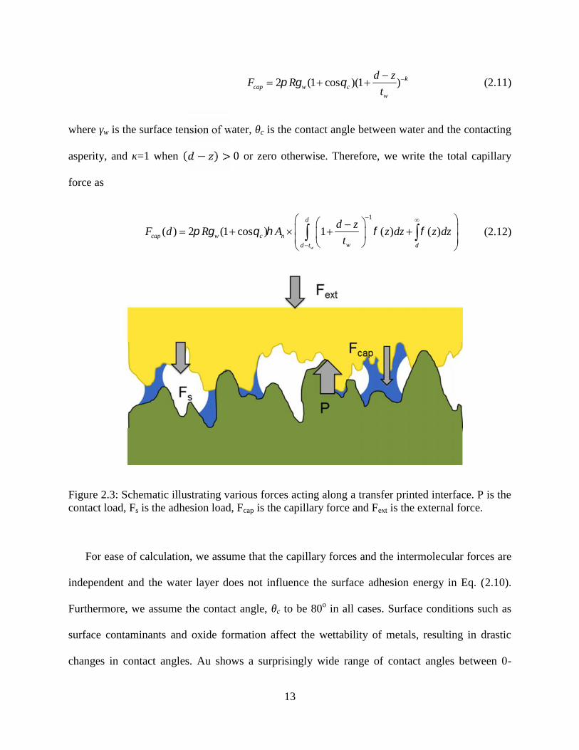
When two surfaces are in contact, four forces, namely the contact load P, the external force
Fex, the adhesion force Fs, and the capillary force Fcap balance each other as = + +as shown in figure 2.3. When an external force is absent, the contact load must balance the
adhesion force and the capillary force. While the original work from Greenwood and Williamson
does not include consideration of adhesion forces, Johnson et al.21 and Derjaguin et al.22
proposed two different models, the JKR model and the DMT model respectively, to consider
adhesion between an elastic sphere and a flat surface. The major differences between these
models are that the JKR model assumes that the adhesion forces lie within the contact area and
increase the area of contact, while the DMT model predicts that the adhesion forces are exerted
only outside the contact area and have no effect on the deformation of the sphere. Previous
work23 has concluded that the JKR and the DMT models are both limiting cases of a general
solution: The JKR model holds for materials with low elastic modulus while the DMT model
holds for materials with high elastic modulus. Therefore, the DMT model is more suitable for

12
metallic contacts. Here, we apply the DMT model in the subsequent calculations and include a
modification introduced by Muller et al.24 The original DMT model only considered a sphere in
contact with a flat surface. Instead, Muller et al.24 assumed the dominant adhesion force to be the
van der Waals force and the total intermolecular force to follow the Lennard-Jones surface
pressure given by
3 98
( )3
p zz z
(2.9)
where Δγ is the energy of adhesion, ε is the intermolecular distance ranging between 0.3 and 0.5
nm, and z is the separation of the contacting sphere and the flat surface outside the contact area.
Using this, we can write the dimensionless adhesion force ∗ predicted by the KE model as
* * * * * **
* * * * *
6 110* * 0.298 0.356 0.093
0.29 0.321 0.332
6
( ) 2 0.98 0.79 1.19c c c
c c
d d dds
s ncn d d d
FF d R J J J J
A H H
.
(2.10)
where the integrand for the contribution of the non-contacting asperities is
2 8* *
* * * *
40.25
3ncJd z d z
and the general form of the integrand for the contribution
of the contacting asperities is* * *
* * ** *
( )c c
z dJ z dz
.
For the consideration of capillary forces, here we assume a monolayer of water with
thickness, tw=0.278 nm at the surface. The formation of water droplets on the surface follows the
Kelvin equation.25 The resulting force applied to an individual asperity is26
13
2 (1 cos )(1 )cap w cw
d zF R
t
(2.11)
where γw is the surface tension of water, θc is the contact angle between water and the contacting
asperity, and κ=1 when ( − ) > 0 or zero otherwise. Therefore, we write the total capillary
force as
1
( ) 2 (1 cos ) 1 ( ) ( )w
d
cap w c nwd t d
d zF d R A z dz z dz
t
(2.12)
Figure 2.3: Schematic illustrating various forces acting along a transfer printed interface. P is thecontact load, Fs is the adhesion load, Fcap is the capillary force and Fext is the external force.
For ease of calculation, we assume that the capillary forces and the intermolecular forces are
independent and the water layer does not influence the surface adhesion energy in Eq. (2.10).
Furthermore, we assume the contact angle, θc to be 80o in all cases. Surface conditions such as
surface contaminants and oxide formation affect the wettability of metals, resulting in drastic
changes in contact angles. Au shows a surprisingly wide range of contact angles between 0-

14
84o.27-30 While our choice of contact angle is nominal, we note that using a contact angle of zero
increases both the contact area and the thermal conductance by ~23%.
Figure 2.4 shows the contact load and the adhesion forces as a function of separation from
the mean of asperity heights. Wet adhesion refers to the inclusion of the capillary force and dry
adhesion refers to the exclusion of this force in the calculations. We show the calculations for the
CEB model for comparison. The KE model predicts the force balance at a separation of ~ (- σ)
whereas for CEB model the balance occurs at ~ (-4 σ). Considering the highly malleable
characteristics of Au, the prediction of the KE model is reasonable while that of the CEB model
is clearly not. For both models, the contact load increases as the mean separation decreases,
while the rate of increase slows around 0.35 nm. The latter is comparable to the standard
deviation of surface heights, σ. For the KE model, both wet and the dry adhesion are maximum
around a mean separation of zero, and decrease when the separation decreases further. As given
in Eq. (2.10), the fully plastic contact becomes more significant as the separation becomes
smaller. However, the effect of adhesion force due to the fully plastic contact is smaller than
forces in other deformation modes, and thus overall, the adhesion forces decline.

15
Figure 2.4. Comparisons between the CEB (solid lines) and the KE (dashed lines) models in thecalculations of the contact load P and the adhesion force Fs. Dry adhesion excludes watercapillary forces while wet adhesion includes this. The force balance between the contact load andthe adhesion forces happens at ~(− ) for the KE model and at ~(−4 ) for the CEB model.
We next investigate the change in the contact area with increasing temperature. We obtain
temperature dependent parameters for Au and SiO2 surfaces from the literature.31-33 The main
temperature dependence is in the Young’s modulus and hardness of Au that decrease with
increasing temperature, resulting in greater deformation of contacting asperities. Figure 2.5
shows the calculated contact area as a function of temperature for the Au-SiO2 interface. In the
case of dry adhesion, the contact area increases marginally from ~10% to ~11% as temperature
increases from 300K to 600K due to increased deformation as discussed above. However in the
case of wet adhesion, the dominant adhesion force due to surface tension decreases as

16
temperature increases which leads to lesser augmentation of contact area due to capillary forces
at higher temperatures. This results in a steep decrease in the contact area from ~21% to ~13%
for the same temperature change of 300K.
Figure 2.5. The actual contact area between Au and SiO2 surfaces as a function of temperature.For dry adhesion, the contact area increases due to decrease in the Young’s modulus E andhardness H of the softer material, Au in this case. In wet adhesion, the area decreases since thesurface tension of water decreases as temperature increases.
A key parameter affecting the area of contact is the plasticity index, = ( ) ⁄that indicates the degree of elastic and plastic deformation. According to Kogut and Etsion18,
deformation transitions from elastic to elastic-plastic around ~√2 and asperities start reaching
fully plastic deformations only if > 6. In order to investigate the influence of the plasticity
index on the actual contact area, we examined eight different metals as shown in table 2.1.

17
Al Au Ag Cu Pt Ni Cr W
E (GPa) 70 78 83 120 168 200 279 411
Ν 0.35 0.44 0.37 0.34 0.38 0.31 0.21 0.28
H (GPa) 0.167 0.216 0.251 0.369 0.549 0.638 1.06 3.43
Ψ 11.6 9.19 8.27 6.56 4.81 4.47 3.08 0.971
Table2.1.Material properties of various metals at 300K. The plasticity index is determined bythe mechanical properties of contacting materials and the surface roughness parameters, andindicates the degree of elastic and plastic deformation in each case.
Assuming that the energy of adhesion between the metal and the nonmetal arises from
London dispersion forces, the range for adhesion energy of most metals is quite narrow, within
0.06-0.1 Jm-2.34 In these calculations, we assumed the energy of adhesion to be constant at
Δγ=0.1 Jm-2. Figure 2.6 shows resulting contact areas for these materials, assuming roughness
similar to that for Au. The actual contact area is proportional to the plasticity index with the trend
slowing at ~8. This trend agrees well with previous results.18 Figure 2.6 also shows the contact
area under wet adhesion. The contact area increases ~2 times compared to dry adhesion, for most
metals. From this we infer that it is the combined effect of plastic deformation and capillary
forces which leads to significant enhancement of contact area. We show later that the interfacial
thermal conductance for different transfer-printed metallic films is strongly dependent on the
plasticity index.

18
Figure 2.6.Predictions of the actual contact area for different metals showing the strongdependency of the contact area on the plasticity index. Blue dots represent wet adhesion and reddots represent dry adhesion. The contact area linearly increases when the index is low( < 6),but the trend slows once the index becomes larger than 8.

19
3. MICROSCOPIC COMPONENT OF THERMAL CONDUCTANCE
3.1 Diffuse Mismatch Model (DMM)
Thermal resistance at the interface of two solids is observed even for atomically perfect
interfaces. The origin of this resistance, named as the microscopic component here, is different
from macroscopic component. Two models, namely, Acoustic Mismatch Model (AMM) and
Diffuse Mismatch Model (DMM) have been proposed to explain the origin and calculate this
thermal resistance.4 In AMM, the phonons are treated as waves, the solids are treated as
continua, the interface is treated as a plane and the phonon propagation is governed by
continuum acoustics. The interfacial thermal resistance is then explained based on different
acoustic impedances of the two solids which depends on properties like density and speed of
sound in the solid. The wave picture of phonon is not valid at room temperature for typical vapor
deposited interfaces, when the wavelength of thermally excited phonons (~0.1 nm) is comparable
to the interfacial roughness. For such cases, DMM is better applicable.
The idea behind DMM is that the phonons are scattered diffusely at the interface and as a
result phonon wave vector and polarization is completely randomized. If α, i and j represent the
probability of transmission of a phonon across the interface, index for medium from which the
phonon transmits (i=1, 2) and polarization of phonon (j=1, 2, 3) then because of randomization
of polarization and wave vector
, ( ( )) ( )i j ik
(3.1)
where ω is the frequency and k is the wave vector of phonon. Also since a phonon is randomized
after scattering, there is no way of telling whether a phonon in a particular medium has arrived

20
after transmission from the other medium or after reflection at the interface in to the same
medium. This gives 1 2 2 11 , 1 .
To calculate α, principle of detailed balance is applied. The number of phonons of frequency
ω leaving side 1 per unit time per unit area is2 /2
1, 1 1,
0 0
( , ) ( ) cos sinj jj
N T c d d
where N1,j is the phonon density of states per unit solid angle for jth polarization and c1,j is speed
of sound for that particular polarization. Assuming that the solids are isotropic Debye solids we
get
2
1, 3 31,8 exp / 1j
j b
Nc k T
. Similarly the number of phonons of frequency ω leaving
side 2 per unit time per unit area is given by2 /2
1, 2 1,
0 0
( , ) ( ) cos sinj jj
N T c d d
.
According to the principle of detailed balance the number of phonons of a particular state leaving
a particular side must be equal to the number of phonons in the same state returning from other
side at thermal equilibrium which means that the number of phonons leaving side 1 and side 2
must be equal. Equating the expressions and using the relationship between transmission
probabilities we get
22, 2 2
2, 2,1 2 2 2 2 2
, 1, 1, 2, 2,
2( )
2 2
jj t l
i j t l t li j
cc c
c c c c c
(3.2)
where l and t represent the longitudinal and transverse modes respectively.
The net heat flow rate from material 1 to 2 is then the difference between the gross heat flow
from side 1 to side 2, when side 1 is at temperature T1 and the gross heat flow from side 2 to side
1 when side 2 is at temperature T2. Using the principle of detailed balance, gross heat flow from

21
side 2 to side 1 when side 2 is at temperature T2 is same as the gross heat flow from side 1 to side
2 when side 1 is at temperature T2. From this, the net heat flow rate from side 1 to side 2 is given
by:
1,
1 2 1 1 2 2
2 /21 2
1, 1 1,
0 0 0
( ) ( )
( )cos sin
Debye
net
j jj
dQ dQ T dQ T
dt dt dt
dQ TN c d d d
Adt
(3.3)
where ω1,Debye is the Debye cut-off frequency of material 1 and A is the area of cross section. Net
heat flow is related to thermal conductance by 1 2( )netph ph
dQG A T T
dt where Gph-ph is the
interfacial thermal conductance. The subscript ph-ph represents the interaction between phonons
on both sides and its relevance will become clear in the next section. From the above expression,
Gph-ph can be calculated in the limit 1 2 0T T as
1,
1,1, 1,
0
/2
1, 1
0
2
cos sin
Debye
jph ph j j
j
j
dNG c d
dT
d
(3.4)
The above discussion holds good for atomically perfect interfaces. The transmission
coefficient is further modified because of scattering at irregular shaped asperities.13 The
dominant wavelength of thermally excited phonons in Au, λD is ~0.1 nm when estimated from
the Debye theory as λD = 2πħv/(kbT), where v is the Debye speed. As calculated in previous
chapter for Au, R is 136 nm and the constriction radius, a, for dry and wet adhesion are 8 nm and
12 nm respectively. Since R>˃ λD and a>˃ λD, there is an additional geometrical scattering. The
effect of geometric scattering is taken into account by multiplying the transmission coefficient by

22
cosθ. Following the similar steps for calculation we get the relationship: , ,
2
3ph ph ballistic ph phG G .
However, the modified value gives a lower bound of the interfacial thermal conductance because
the condition for geometric scattering takes place only at certain locations.
3.2 Electron-Phonon thermal Conductance
DMM values match the experimental values reasonably well for interfaces formed by contact
of dielectric surfaces when the dominant heat carriers are phonons. Intuitively, DMM should not
hold good for metal-dielectric interfaces as the dominant heat carriers in metal are electrons and
heat needs to be transported from electrons in metal to phonons in dielectric. Experimentally, this
has been confirmed and measurements of the thermal conductance at metal-dielectric interfaces
are generally in poor agreement with DMM values. Some of the earlier thermal conductance
measurements5,6 revealed that DMM overestimates or underestimates the experimental values
depending on the mismatch in the Debye temperatures of the metal and the dielectric. When the
Debye temperature ratio of metal to dielectric is greater than 0.4, DMM overestimates the
conductance.6 The various mechanisms proposed in literature for energy transport are shown in
figure 3.1. [A] represents the transfer of energy from electrons in metal to phonons in metal.7 [B]
represents the transfer of energy between phonons in metal to phonons in dielectric via elastic
process described by DMM.4 [C] represents the transfer of energy between phonons via inelastic
processes.35 [D] represents the transfer of energy between phonons in metal and dielectric via the
interfacial mixing zone36 and [E] represents the transfer of energy between the electrons in metal
to phonons in dielectric directly.37 For the cases when DMM under-predicts the experimental
value, pathway [C] provides an explanation. For this case when the Debye temperature of metal

23
and dielectric are widely mismatched, two phonons of lower frequency on metal side can
combine and create a phonon of higher frequency on dielectric side. Energy conservation
dictates:
,max
2
2
metal metal dielectric
dielectric metal
dielectric Debye metal
(3.5)
As long as (ωdielectric)max is less than Debye cut-off frequency of dielectric, the three phonon
process can occur. The theoretical temperature trend of this mechanism has been verified
experimentally for widely mismatched interfaces.35 Pathway [E] had been proposed for
explaining the underestimation of thermal conductance by DMM for a Pb-Diamond interface,37
however, it was shown later that this could not be the possible mechanism.35 Pathway [D] has
been shown to be a probable cause for lowering of experimental conductance as compared to
DMM.36 According to this theory, there is a mixing zone near the interface where the properties
are intermediate to the two substrate materials. It has been shown that additional scattering of
phonons in this zone lowers the probability of transmission and reduces the thermal conductance.

24
Figure 3.1. Various modes of thermal transport across a metal-dielectric interface involvingelectrons (e-) and phonons (ph). [A]: e- (metal) to ph (metal), [B] and [C]: ph (metal) to ph(dielectric) via elastic and inelastic processes respectively (see Ref. 19 & H. Lyeo and D.G.Cahill, Physical Review B 73 (14), 144301(2006)), [D]: ph (metal) to ph (dielectric) through theinterfacial mixing zone (see Ref. 20) and [E]: e- (metal) to ph (dielectric) (M.L. Huberman andA. W. Overhauser, Physical Review B 50 (5), 2865(1994)).
In this work, we will consider the pathway [A]+[B]. Thermal conductance for pathway [B] is
given by DMM as discussed previously. Now we will focus our attention on calculating electron-
phonon thermal conductance for pathway [A] which is referred to as Ge-ph here. The commonly
cited approach to calculate Ge-ph is to consider a two-temperature model7,38,39 where electrons at
temperature Te exchange energy with phonons at temperature T. Under conditions of strong non-
equilibrium between the two, the energy transfer rate becomes proportional to the difference of
the fifth power of the temperatures38. Assuming a small departure from equilibrium, an energy

25
balance based on the Fourier law7 yields an electron-phonon thermal conductance, =, where G is the electron cooling rate and kp is the phonon thermal conductivity of the
metal. As explained below, the latter model remains largely empirical since Ge-ph is commonly fit
to the interfacial thermal conductance data. In this work, we adopt an alternate approach to
obtain Ge-ph directly from the Bloch-Boltzmann-Peierls formula for electron-phonon interaction
that provides an improved assessment of the role of the electron-phonon thermal conductance in
interfacial thermal transport.
As discussed above, a commonly used approach in the literature is to express the electron-
phonon thermal conductance as = . However, the phonon thermal conductivity of
the metal, kp, is usually unknown due to the dominance of the electronic contribution to thermal
conductivity. To proceed with this model, the electron-phonon conductance is assumed to be of
the form = √⁄ , where is an empirical constant obtained from fitting thermal
conductance data. This approach yields the value of Ge-ph within a range of 0.3-1 GW/m2K.
Overall, the model is ambiguous since the empirical parameter needed to calculate electron-
phonon thermal conductance must be extracted from the total interfacial conductance after
accounting for the phonon-phonon conductance estimated from DMM. Further, the assumed
temperature dependence kp~T-1 used in such calculations is only valid for temperatures above the
Debye temperature. A more accurate description would require the fitting of the parameter using
the temperature dependence of kp in three different regimes: T <<D, T >>D and T ~D where D
is the Debye temperature of the metal.
Here, we introduce an approach to obtain Ge-ph valid over a wide temperature range without
requiring any fitting to the thermal conductance data. Our method uses an empirical deformation

26
potential to describe the matrix element, but the approach remains advantageous in that the
empirical fit is to electrical resistivity data and is decoupled from the thermal conductance data.
Thus, the predicted electron-phonon thermal conductance is independent of the
validity/reliability of the DMM predictions of the phonon-phonon thermal conductance. We
argue that this provides a better answer to the question whether electron-phonon coupling can
indeed explain the discrepancy between the experimental thermal conductance of metal-
dielectric interfaces and predictions of the theoretical diffuse mismatch model (DMM).
We start our formulation by assuming that electrons are in equilibrium at temperature Te and
the phonons are in equilibrium at temperature T. Electrons from an initial quantum state defined
by wave vector k move into final quantum state k` and release/absorb a phonon in the process.
Momentum and energy conservation for the system requires:
2 2 2 2
* *
2 2
`
`q
k k q
k k
m m
ħ ħ
ħ(3.6)
where q and ωq are the phonon wave vector and frequency respectively. The transition
probability for an electron to go from initial state |k> to a final state |k`> is calculated from
Fermi’s golden rule and is given by:
'`
2`2
, | | kkP k k k H k E E
ħ(3.7)
Where Ek’ and Ek are the energies of the final and initial states and the δ-function ensures energy
conservation. Using the above transition probability, conservation laws and Bloch-Boltzmann-
Peierls formula40,41 we get the net rate of change of the phonon occupation due to electron
scattering:

27
2
, 1 ,
2
, 1 ,
| | 12
| | 1
q q
q q
k n k q nq
kk q n k n
k H k q E E f k q f kn
t k q H k E E f k f k q
ħ (3.8)
where nq is the Bose-Einstein occupation number for the phonons with wave vector q, k is the
initial electron wave vector, H is the interaction Hamiltonian for electron-phonon scattering, f is
the Fermi distribution given by2 2
( ) *
1( ) ; ( )
21
F
BTe
E k E
k
kf k E k
me
and E is the energy of the
electron-phonon system.
We employ deformation potential theory42,43 to describe the interaction Hamiltonian for
electron-phonon scattering process as
ac ac
VH D D divu r
V
(3.9)
where Dac is the deformation potential for electron scattering by acoustic phonons, V is the
volume and u(r) is the displacement vector at position r. Using the Hamiltonian of Eqn. (3.9) the
matrix element for electron-phonon interaction can be written as:
2 22`
2
1 1 1 1| |
2 2 2 2 2 2ac q ac
q qs s
D D qk H k n n
Vdv Vdv
ħ ħ(3.10)
where d is the density of the metal and vs is the speed of longitudinal waves. Here we use the
Debye density of states for phonons. The positive sign inside the brackets indicates phonon
emission and the negative sign indicates phonon absorption.
The electron-phonon scattering time can be expressed in terms of the deformation potential
as43

28
4 2
* 3/2 2
2( )
(2 )s
ac b
dvE
m D k T E
(3.11)
Using the known relation between the electrical resistivity due to phonon scattering and the
average electron scattering time: = ∗( ), we get a direct relation between resistivity
and the deformation potential. This relation is,
4 2 22
3*2 2
5
2 1( )( )
(2) ( ) B
e phsac
F
v eD
d n
T Em k
ħ
(3.12)
where e-ph is electrical resistivity omitting the low temperature residual resistivity and can be
readily obtained from the total resistivity using Matthiessen’s rule. We have calculated the best-
fit value for Dac for six metals (Au, Al, Ag, Cr, Cu and Pt) using multiple linear regression over
the temperature range and found the values to be 4.50, 6.37, 3.70, 14.70, 5.22 and 10.12 eV
respectively. For T>D, the variation in Dac with temperature is <10% for these metals. The
discrepancy between Ge-ph calculated using the exact temperature dependent Dac compared to
that from the best fit temperature independent value is also <10% for all the metals listed here
expect for Au and Cr where it is as much as 40%. The temperature independence can be
understood by considering, for example, the Bloch-Gruneisen formula for electrical resistivity40
due to electron-phonon scattering:5 / 5
0 ( 1)(1 )
D T
e ph x xD
T xA dx
e e
. This yields Dac
independent of T for T>D, with4 2 2
23 5
2 2
2 1
42 *
sac
DFB
dv ne AD
Em k
. In our calculations, we found

29
Dac to be essentially constant for T>0.1D. When T≪D,
/4 2 2 4 52
3 5 502 2
2 1
( 1)(1 )2 *
D T
sac x x
DFB
dv ne T xD A dx
e eEm k
and is temperature dependent.
To simplify Eqn. (3.3) we covert summation over k space into integral as:
*
22
30 0
( )2
2sin
2s
k m vqk
VF k F k k d d dk
ħ
(3.13)
The lower limit on k comes from energy conservation. The additional factor of 2 along with the
usual factor of V/(2π)3 comes from the fact that electrons of both spins can participate in
scattering. After the integration over Ѳ space, Eqn. (3.8) simplifies to:
*
22 *
2 20
( )2
( 1 14
(1 )]
s
q acq
s m vqk
q
d
n D md dk k n f k q f k
t v
n f k f k q
ħ
ħ(3.14)
At room temperature, the term (m*vs/ħ) is small compared to (q/2) and can be neglected. Finally,
the net rate of energy exchange between electrons and phonons is
32
0
( ) 2
D
qs
q
qqs
q
ndQv q
dt t
nv Vq dq
t
ħ
ħ(3.15)
where qD is the Debye wave vector. Expressing the energy balance between electrons and
phonons as
e ph e
dQG A T T
dt (3.16)

30
where A is the cross-sectional area. We then obtain the electron-phonon conductance as
3 32 2
0 02 ( ) 2 ( )
D Dq qq qs s
e phe eq q
n nv V v LG q dq q dq
A T T t T T t
ħ ħ
(3.17)
where L is the characteristic length scale for energy transfer. Here we choose L=fΛe where Λe is
the electron mean free path in the metal. We use a value of 3 for f corresponding to ~95% energy
loss.44 We note that this is different from the effective length scale for energy transfer in Ref.
[10] where it is given by . In the latter case, the length scale is only a fraction of the
electron mean free path and seems unphysical. Eqn. (3.12) can be simplified using Eqn. (3.17) as
2 2
2 2
11 ( )/2 * 8 *3
0
2
8 *
3 3
11 1 ln
(1
)4
Fs B essD B e
B eB
F
B e B e
E qv q k Tv qv qq k T m
k Tk Tace ph E
B e
q
k T m ke T
D m e eG q e e dq
k T L
d T Te e
ħ
(3.18)
The above expression can be further simplified by expanding the first term inside the integral in
the limit of high temperatures.
In subsequent numerical calculations, we employ the Fermi-Dirac and Bose-Einstein
distribution functions to obtain Ge-ph across a wide temperature range. We have verified that the
computed value of Ge-ph at 300 K is independent of the temperature difference (Te-T). Figure 3.2
shows the variation of Ge-ph with temperature for the six metals up to 500 K. The value of Ge-ph
increases with temperature and becomes approximately constant at room temperature. The values
range between ~0.1-4 GW/m2K at room temperature. Specifically, the values at room
temperature for Au and Al are 0.11 GW/m2K and 1.1 GW/m2K respectively. We compare these
pkl
G

31
with values based on the model of Ref. [10] using measured values of kp45,46 and electron cooling
rates from the two-temperature model.47,48 The latter values are 0.29 GW/m2K and 2.21
GW/m2K respectively49 and are of the same order of magnitude as our predictions but
approximately a factor of 2 larger. We have performed the calculations across a wide
temperature range, both T<< D and T~D. For T<D, our calculations show that Ge-ph~Tn, where
the exponent n ranges between 3.5-3.7 expect for Au where the exponent is 3.1. This is in
agreement with the predicted dependence of Ge-ph from the two-temperature model38 where the
dependence is = ~√ ~ . . We do not compare the temperature trends for
T~D since G does not have a simple analytical power law dependence on T for T~D.50
Figure 3.2. Thermal conductance due to electron-phonon coupling, Ge-ph as a function oftemperature for six metals. The temperature dependence of Ge-ph closely follows ~T3.5 at lowtemperatures (T/D<0.1).

32
We now investigate the relative contribution of the electron-phonon conductance to the net
thermal conductance for several metal-dielectric interfaces. The diffuse mismatch model
provides Gph-ph, the thermal conductance due to the energy transfer between phonons. The net
conductance with Ge-ph and Gph-ph in series is
e ph ph phnet
e ph ph ph
G GG
G G
(3.19)
We have computed Gnet as a function of temperature for all the six metals mentioned above
with silicon, silica, sapphire and diamond as the dielectric. For interfaces whose vibrational
spectra are similar (Debye temperatures approximately equal), GDMM is considered to be a
reasonable estimate of the phonon-phonon interfacial thermal conductance. In such cases, the
discrepancy between GDMM and Gnet from measurements varies between ~3-7 times at room
temperature.6,51 In our calculations, GDMM never exceeded Gnet by a factor greater than 2 for
T>200 K. The maximum remains 1.8 for an Al-SiO2 interface. Figure 3.3 plots the absolute
difference between Gnet and GDMM as a fraction of GDMM for silicon and sapphire interfaces with
Al, Au, Cr and Pt. Thus, our numerical calculation of electron-phonon thermal conductance
shows that the electron-phonon coupling is not a plausible reason for the observed discrepancy at
room temperature. Our theory also extends to T<D where GDMM exceeds the calculated total
thermal conductance by a factor of up to 5 but this factor falls off quickly to less than 2 as we
reach 50 K. Thus, our results are consistent with recent work that suggests other factors such as
interface defects5,6,36 are responsible for the reduction in Gnet.

33
Figure 3.3. The difference between GDMM and Gnet as a fraction of GDMM for interfaces of Au, Al,Cr and Pt with (a) Si and (b) sapphire.
We note that while the analysis in this work assumes linear phonon dispersion, it is fairly
straightforward to extend the analysis to non-linear dispersion. We have verified that this does
not alter the conclusion and Ge-ph predictions remain of the same order of magnitude. We
considered a more accurate sinusoidal dispersion.52 The comparison between linear and sine
dispersion for Au is shown in figure 3.4. The values of Ge-ph increase from those corresponding
to linear dispersion by as much as 180% for Al and <140% for other metals. For T>200K, the
increase is modest, between 25-65% across all the metals considered in our work. Previous
work5 has considered the effect of non-linear phonon dispersion on GDMM for Au and Al
interfaces with diamond and sapphire, finding that values decrease by a factor as much as 3.7.
Consequently, the inclusion of non-linear dispersion would increase the ratio of Ge-ph to GDMM
and render the electron-phonon thermal conductance even more insignificant. Our conclusions
thus remain the same irrespective of phonon dispersion. Thus by studying the net thermal
conductance across several metal-dielectric interfaces, we find that electron-phonon coupling
does not add significant thermal resistance to the DMM resistance at temperatures above 200 K.

34
We hypothesize that the discrepancy between the experimental and DMM values of thermal
conductance is likely due to other factors such as interface substrate damage, interfacial mixing
and interfacial defects due to lattice mismatch5,6,36. We conclude that electron-phonon coupling
for such interfaces can be ignored in considerations of thermal transport.
Figure 3.4. Comparison between Ge-ph calculated using linear and more accurate sine dispersionfor gold.
Even though we have shown that electron-phonon thermal conductance can be ignored due to
its higher value as compared to DMM value, we include it in the subsequent analysis for better
accuracy. We have calculated Gnet, the harmonic sum of Ge-ph and GDMM. To calculate Gmicroscopic ,
we scale Gnet with the contact area ratio as:

35
2 ( )microscopic net dG G a z dz
(3.20)

36
4. NET THERMAL CONDUCTANCE: THEORETICAL v/s OBSERVED
4.1 Net thermal conductance for transfer printed interfaces
We have calculated Gmacroscopic and Gmicroscopic in the previous chapters. These two
conductances act in series and as a result, the net thermal conductance for a transfer printed
interface is given by:
macroscopic microscopic
macroscopic microscopic
G GG
G G
(4.1)
We now compare the results of the above theory with experimental data12 on interfacial thermal
conductance of Au-SiO2 and Au-Si interfaces in the temperature range 300-600 K. Figure 4.1
plots the experimental and theoretical conductance across the two interfaces. Wet and dry
adhesion result in different areas of contact and hence, differing thermal conductances. Further,
the inclusion of geometric scattering in the phonon-phonon conductance provides a lower limit
to conductance as discussed previously and is plotted separately in the case of Au-SiO2.
Inclusion of ballistic effects reduces the conductance by a third. However, this will only be
present are certain locations and provides the lower bound on thermal conductance. Overall, wet
adhesion augments the thermal conductance significantly, more than doubling the conductance at
300 K, in comparison to dry adhesion.

37
Figure 4.1 Comparison of theory with experimental data on the interfacial thermal conductancebetween (a) Au-SiO2 and (b) Au-Si as a function of temperature. Wet adhesion significantlyenhances conductance but the predictions still underestimate the measured values.

38
The predicted conductance for wet adhesion is of the same order of magnitude as the
measured value indicating the significance of plastic deformation in providing a relatively large
area of contact for heat conduction. The predicted value for Au-SiO2 varies between ~18
MW/m2K at 300 K to ~9 MW/m2K at 600 K. The decreasing temperature trend in the case of
wet adhesion agrees well with the general trend of the experimental data giving further credence
to the argument that wet adhesion is involved in these interfaces. Temperature dependence arises
entirely due to temperature dependent mechanical properties that affect deformation mechanics.
Standard DMM predicts an approximately constant conductance at temperatures above the
Debye temperature. In the case of Au-Si, the predictions again underestimate the data. The
somewhat larger difference is due more to the smaller DMM predictions rather than a
dramatically reduced role of plastic deformation. Overall, there remains a significant quantitative
discrepancy between theory and experiments in both these interfaces.
4.2 Conduction through capillary bridges
We speculate that the discrepancy arises due to heat conduction via capillary bridges.
Previous ultrafast thermoreflectance experiments on the Au-water interface measured G>20
MW/m2K.53 The conductance increases as the surface becomes more hydrophilic. While low
frequency phonons transport heat independent of the interfacial bonding, high frequency
phonons transmit better as the interface bonding strengthens. Molecular simulations54 also
corroborate the measurements and further reveal that the conductance is directly proportional to
the work of adhesion. An upper limit to the conductance is unknown at present but the value can
exceed 100 MW/m2K .49

39
Assuming that water capillaries conduct heat parallel to solid-solid contacts, the product of
the net conductance of capillary bridges and the fractional area available for such conduction,
Gcapillary Acapillary/An, should equal ~30 MW/m2K in the case of Au-SiO2 at 300 K. The latter is
the net difference in the measured conductance and the calculated conductance in Fig. 4.1(a).
Assuming a similar areal fraction under water capillary as the solid-solid contact, the required
conductance across the capillary is ~120 MW/m2K. This appears reasonable based on existing
experiments49,53 and simulations54 where the reported range is 20-300 MW/m2K. The actual areal
coverage of water capillaries is difficult to estimate directly55 based on the current state of
research, especially for a distribution of asperities across different length scales. Since the
average separation between surfaces is <1 nm (comparable to the roughness deviation), the
behavior of water is likely not that of the bulk. While theories for the structure of water at sub-
nm asperities exist56, considerations of heat conduction through such structures are absent in the
literature. More insight in this problem requires measurements with controlled humidity in
tandem with molecular simulations. We do note that existing molecular simulations of a broad
range of surface chemistries suggest the absence of a water vapor layer at the interface even
when hydrophobic54,56-58, suggesting that conduction via water capillaries could contribute
significantly.
Finally, we present the estimated thermal conductance for different metal-dielectric
interfaces assuming similar roughness profiles. Figure 4.2(a) shows the conductance for different
metals with SiO2 as the substrate. The figure shows both wet and dry adhesion. The values are on
the order of 10 MW/m2K for the case of wet adhesion, suggesting good conductance for most
metals used in transfer printing. The variation amongst metals is largely the consequence of

40
differing plasticity indices. Figure 4.2(b) plots the conductance between Au and various
substrates. The variation in this case is related more to phonon-phonon conductance.

41
Figure 4.2 Interfacial thermal conductance at room temperature for various metal-dielectricinterfaces. (a) The calculations are for different metals with SiO2 as the substrate at roomtemperature. Al shows the highest interfacial thermal conductance and Au the lowest. (b) Thesame calculation for the interface between Au and various substrates.

42
5. SUMMARY AND CONCLUSIONS
In this work, we have considered two of the main factors controlling the interfacial thermal
conductance for metal-dielectric interfaces: electron-phonon coupling in the metal and fractional
area coverage at the interface. The effect of electron-phonon coupling on the thermal
conductance for metal-dielectric interfaces is not clearly understood. The leading model is semi-
empirical in nature and it depends on the thermal conductance measurements for the calculation
of empirical parameter. We have developed a model of the thermal conductance due to electron-
phonon coupling that can be calculated independent of thermal conductance measurements. The
current work is based on the scattering theory of electrons and phonons and the empirical
parameter needed for calculation is extracted from the electrical resistivity data that is more
reliable than the procedure adopted in the previous model. We find Ge-ph to range between 0.1-4
GW/m2K at room temperature across six different metals. For T<D, the temperature dependence
of Ge-ph predicted by our model is in agreement with that from the two-temperature model. By
studying the net thermal conductance across several metal-dielectric interfaces, we find that the
electron-phonon coupling does not add significant thermal resistance to the DMM resistance at
temperatures above 200 K. We hypothesize that the discrepancy between the experimental and
the DMM values of the thermal conductance is then likely due to other factors such as interface
substrate damage, interfacial mixing and interfacial defects due to lattice mismatch. We conclude
that electron-phonon coupling for such interfaces can be ignored in considerations of thermal
transport and hence, provide an answer to whether the electron-phonon thermal conductance
should be considered for metal-dielectric interfaces. Based on our work, the microscopic thermal
conductance can be directly estimated by the DMM.
43
Macroscopic component which is due to the constriction of actual contact area as compared
to the nominal area, gains relative importance in limiting thermal transport for rough interfaces.
For transfer-printed Au-dielectric interfaces with sub-nanometer roughness, we have shown that
the plastic deformation of Au, in combination with capillary forces leads to a large fractional
area of coverage (~0.25). Such a high value of fractional area coverage shows that the transfer
printed interfaces are not at a big disadvantage as compared to the interfaces formed by vacuum
deposition in terms of contact area. From the comparison of fractional area coverage for dry and
wet adhesion, we conclude that the capillary forces augment the contact area by more than two
times as compared to dry adhesion at room temperature. Also, the temperature trends of contact
area for wet and dry adhesion cases are different and opposite in nature.
Finally, the net thermal conductance has been calculated as the series sum of macroscopic
and microscopic thermal conductances. The calculations show the value of interfacial
conductance to be ~10 MW/m2K, comparable in magnitude to the experimental data. The
temperature trend of net thermal conductance further agrees with experimental data giving
credence to wet adhesion hypothesis. We attribute the discrepancy between theory and data to
conduction via water capillary bridges. We support this hypothesis with a preliminary numerical
analysis. Further experimental and theoretical verification remains a topic of future research.
44
REFERENCES
1 Sarua, A. et al. Thermal boundary resistance between GaN and substrate in AlGaN/GaNelectronic devices. Electron Devices, IEEE Transactions on 54, 3152-3158 (2007).
2 Prasher, R. S. & Phelan, P. E. Microscopic and macroscopic thermal contact resistances ofpressed mechanical contacts. Journal of Applied Physics 100 (2006).
3 Madhusudana, C. Thermal contact conductance. (Springer, 1996).4 Swartz, E. T. & Pohl, R. O. Thermal boundary resistance. Reviews of Modern Physics 61, 605-668
(1989).5 Stoner, R. J. & Maris, H. J. Kapitza conductance and heat flow between solids at temperatures
from 50 to 300 K. Physical Review B 48, 16373-16387 (1993).6 Stevens, R. J., Smith, A. N. & Norris, P. M. Measurement of Thermal Boundary Conductance of a
Series of Metal-Dielectric Interfaces by the Transient Thermoreflectance Technique. Journal ofHeat Transfer 127, 315-322 (2005).
7 Majumdar, A. & Reddy, P. Role of electron--phonon coupling in thermal conductance of metal--nonmetal interfaces. Applied Physics Letters 84, 4768-4770 (2004).
8 Frank, D. J. et al. Device scaling limits of Si MOSFETs and their application dependencies.Proceedings of the IEEE 89, 259-288, doi:10.1109/5.915374 (2001).
9 Bass, J. & Pratt Jr, W. P. Spin-diffusion lengths in metals and alloys, and spin-flipping atmetal/metal interfaces: an experimentalist's critical review. Journal of Physics: CondensedMatter 19, 183201 (2007).
10 Oh, D.-W., Kim, S., Rogers, J. A., Cahill, D. G. & Sinha, S. Interfacial Thermal Conductance ofTransfer-Printed Metal Films. Advanced Materials 23, 5028-5033, doi:10.1002/adma.201102994(2011).
11 Kim, D. H., Xiao, J., Song, J., Huang, Y. & Rogers, J. A. Stretchable, curvilinear electronics basedon inorganic materials. Advanced Materials 22, 2108-2124 (2010).
12 Oh, D. W., Kim, S., Rogers, J. A., Cahill, D. G. & Sinha, S. Interfacial Thermal Conductance ofTransfer-Printed Metal Films. Advanced Materials 23, 5028-5033, doi:Doi10.1002/Adma.201102994 (2011).
13 Prasher, R. Ultralow thermal conductivity of a packed bed of crystalline nanoparticles: Atheoretical study. Physical Review B 74, 165413 (2006).
14 Cooper, M. G., Mikic, B. B. & Yovanovi.Mm. Thermal Contact Conductance. International Journalof Heat and Mass Transfer 12, 279-& (1969).
15 Greenwood, J. A. & Williamson, J. B. P. Contact of Nominally Flat Surfaces. Proceedings of theRoyal Society of London Series a-Mathematical and Physical Sciences 295, 300-& (1966).
16 Timoshenko, S. & Goodier, J. N. Theory of Elasticity, by S. Timoshenko and J. N. Goodier,... 2ndEdition. (McGraw-Hill book Company, 1951).
17 Chang, W. R., Etsion, I. & Bogy, D. B. An Elastic-Plastic Model for the Contact of Rough Surfaces.Journal of Tribology-Transactions of the Asme 109, 257-263 (1987).
18 Kogut, L. & Etsion, I. A finite element based elastic-plastic model for the contact of roughsurfaces. Tribology Transactions 46, 383-390 (2003).
19 Kogut, L. & Etsion, I. Adhesion in elastic-plastic spherical microcontact. Journal of Colloid andInterface Science 261, 372-378 (2003).
20 Mccool, J. I. Comparison of Models for the Contact of Rough Surfaces. Wear 107, 37-60 (1986).21 Johnson, K. L., Kendall, K. & Roberts, A. D. Surface Energy and Contact of Elastic Solids.
Proceedings of the Royal Society of London Series a-Mathematical and Physical Sciences 324,301-& (1971).

45
22 Derjaguin, B. V., Muller, V. M. & Toporov, Y. P. Effect of Contact Deformations on Adhesion ofParticles. Journal of Colloid and Interface Science 53, 314-326 (1975).
23 Muller, V. M., Yushchenko, V. S. & Derjaguin, B. V. On the influence of molecular forces on thedeformation of an elastic sphere and its sticking to a rigid plane. Journal of Colloid and InterfaceScience 77, 91-101, doi:10.1016/0021-9797(80)90419-1 (1980).
24 Muller, V. M., Derjaguin, B. V. & Toporov, Y. P. On 2 Methods of Calculation of the Force ofSticking of an Elastic Sphere to a Rigid Plane. Colloids and Surfaces 7, 251-259 (1983).
25 Thomson, W. On the Equilibrium of Vapour at a Curved Surface of Liquid. Phil. Mag. 42, 448-452(1871).
26 Suh, A. Y. & Polycarpou, A. A. Adhesive contact modeling for sub-5-nm ultralow flying magneticstorage head-disk interfaces including roughness effects. Journal of Applied Physics 97 (2005).
27 White, M. L. The Wetting of Gold Surfaces by Water1. The Journal of Physical Chemistry 68,3083-3085, doi:10.1021/j100792a515 (1964).
28 Erb, R. A. Wettability of gold. The Journal of Physical Chemistry 72, 2412-2417,doi:10.1021/j100853a023 (1968).
29 Smith, R. D. & Berg, J. C. The collapse of surfactant monolayers at the air—water interface.Journal of Colloid and Interface Science 74, 273-286, doi:10.1016/0021-9797(80)90190-3 (1980).
30 Tabor, R. F., Morfa, A. J., Grieser, F., Chan, D. Y. C. & Dagastine, R. R. Effect of Gold Oxide inMeasurements of Colloidal Force. Langmuir 27, 6026-6030, doi:10.1021/la200166r (2011).
31 Merchant, H. D., Murty, G. S., Bahadur, S. N., Dwivedi, L. T. & Mehrotra, Y. Hardness-Temperature Relationships in Metals. Journal of Materials Science 8, 437-442 (1973).
32 Simmons, G. & Wang, H. Single crystal elastic constants and calculated aggregate properties: ahandbook. 2d edn, (M.I.T. Press, 1971).
33 White, F. M. Fluid mechanics. 5th edn, (McGraw-Hill, 2003).34 Varchenya, S. A., Simanovskis, A. & Stolyarova, S. V. Adhesion of Thin Metallic-Films to Non-
Metallic Substrates. Thin Solid Films 164, 147-152 (1988).35 Lyeo, H.-K. & Cahill, D. G. Thermal conductance of interfaces between highly dissimilar
materials. Physical Review B 73, 144301 (2006).36 Beechem, T., Graham, S., Hopkins, P. E. & Norris, P. M. Role of interface disorder on thermal
boundary conductance using a virtual crystal approach. Applied Physics Letters 90, 054104-054103 (2007).
37 Huberman, M. L. & Overhauser, A. W. Electronic Kapitza conductance at a diamond-Pb interface.Physical Review B 50, 2865-2873 (1994).
38 Kaganov, M. I., Lifshitz, I. M. & Tanatarov, L. V. Sov. Phys. JEPT
4, 232-237 (1956).39 Allen, P. B. Theory of thermal relaxation of electrons in metals. Physical Review Letters 59, 1460-
1463 (1987).40 Ziman, J. M. Electrons and Phonons. (Oxford Univ. Press, 1960).41 Conwell, E. M. High Field Transport in Semiconductors. (Academic Press, 1967).42 Bardeen, J. & Shockley, W. Deformation Potentials and Mobilities in Non-Polar Crystals. Physical
Review 80, 72-80 (1950).43 Hamaguchi, C. Basic semiconductor physics. 208 (Springer, 2001).44 Mitchell, D. F. et al. Film thickness measurements of SiO2 by XPS. Surface and Interface Analysis
21, 44-50, doi:10.1002/sia.740210107 (1994).45 Gripshover, R. J., VanZytveld, J. B. & Bass, J. Thermopower of Pure Aluminum. Physical Review
163, 598-603 (1967).

46
46 White, G. K., Woods, S. B. & Elford, M. T. The lattice thermal conductivity of dilute alloys of silverand gold. Philosophical Magazine 4, 688-692, doi:10.1080/14786435908243265 (1959).
47 Hodak, J. H., Henglein, A. & Hartland, G. V. Electron-phonon coupling dynamics in very small(between 2 and 8 nm diameter) Au nanoparticles. The Journal of Chemical Physics 112, 5942-5947 (2000).
48 Tas, G. & Maris, H. J. Electron diffusion in metals studied by picosecond ultrasonics. PhysicalReview B 49, 15046-15054 (1994).
49 Ge, Z., Cahill, D. G. & Braun, P. V. Thermal Conductance of Hydrophilic and HydrophobicInterfaces. Physical Review Letters 96, 186101 (2006).
50 Wang, W. & Cahill, D. G. Limits to Thermal Transport in Nanoscale Metal Bilayers due to WeakElectron-Phonon Coupling in Au and Cu. Physical Review Letters 109, 175503 (2012).
51 Hopkins, P. E., Norris, P. M. & Stevens, R. J. Influence of Inelastic Scattering at Metal-DielectricInterfaces. Journal of Heat Transfer 130, 022401-022409 (2008).
52 Dames, C. & Chen, G. Theoretical phonon thermal conductivity of Si/Ge superlattice nanowires.Journal of Applied Physics 95, 682-693 (2004).
53 Wilson, O. M., Hu, X., Cahill, D. G. & Braun, P. V. Colloidal metal particles as probes of nanoscalethermal transport in fluids. Physical Review B 66, 224301 (2002).
54 Shenogina, N., Godawat, R., Keblinski, P. & Garde, S. How Wetting and Adhesion Affect ThermalConductance of a Range of Hydrophobic to Hydrophilic Aqueous Interfaces. Physical ReviewLetters 102, 156101 (2009).
55 Sirghi, L., Szoszkiewicz, R. & Riedo, E. Volume of a Nanoscale Water Bridge. Langmuir 22, 1093-1098, doi:10.1021/la052167h (2005).
56 Chandler, D. Interfaces and the driving force of hydrophobic assembly. Nature 437, 640-647(2005).
57 Huang, D. M. & Chandler, D. The Hydrophobic Effect and the Influence of Solute−SolventAttractions. The Journal of Physical Chemistry B 106, 2047-2053, doi:10.1021/jp013289v (2002).
58 Hummer, G. & Garde, S. Cavity Expulsion and Weak Dewetting of Hydrophobic Solutes in Water.Physical Review Letters 80, 4193-4196 (1998).