0 investigation of fast reaction saw !accelerometer · investigation of fast reaction saw *...
TRANSCRIPT
MRDC41082. 16FR
Copy No. __.._'o
:0
INVESTIGATION OF FAST REACTION SAW* !ACCELEROMETER
FINAL TECHNICAL REPORT FOR THE PERIODOctober 2, 1980 through September 30, 1984
DARPA ORDER NO. 4061CONTRACT NO. MDA903-81-C-0081
Prepared for DTICDefense Supply Service 7Department of the Army :"LECTE
Washington. D.C. 20310 APR 0 9 198611
M.E. Motamedi U805/373-4479 D D
Approved for public release; distribution unlimited
Sponsored by
Defense Advanced Research Projects Agency (DoD)DARPA Order No. 4061
Under Contract No. MDA903-81-C-0081 issued byDepartment of Army. Defense Supply Service-Washington,
Washington. D.C. 20310
"'Contract effective dates from October 17, 1980 through September 30, 1984".
The views end conclusions contained In this document are those of the authors andshould not be interpreted as necessarily the official policies, either expressed or implied,of the Defense Advanced Research Projects Agency or the U.S. Government.
9l Rockwell International,01%
BBC ILE COPY 49 006 1•. .. ,I ,
-a 2 JA.


V -- -A V 7 *..- 7j*j. - &
Oil Rockwell International
MRDC41O82.16FR
TABLE OF CONTENTS
* Page
4.0 TECMNAL BACKGROUND....... ..... 1 ...... .. ...... .
. 1 SAWOUCIO Acceleomete...... .. 2
. 2 Piezeletri TeGnOAyL..... ... ........ ........ 5 . .
44 . 1 R ceesoatr .t.uctur............................ 9
4.3.2 SAW Resonator Substrate...... ............. o.......... 124.3.3 Frequency and Temperature Stability ............ 124.3.4 SAW Oscillator Testing ....... oo...................... 13
5.0 TECHNICAL APPROACH...... . . . . .................... ...... . . . . 16
5.1 Cantilever Beam Desig g....... . .. .................. .. .. .. .. . . . .. 165.2 Design of SAW Resonator ............................... -... 195.3 Silicon Accelerometer ............. o.............. oo......... 24
5.3.1 Device Structure ...... . o ...... ... .... .... ..... 24
5.4 Guidance System Simulation ...... ....................... ... ... 28
6.1 Fabrication of SAW Resonator ................... .......... 32 V6.2 Test Box Assembly................. ........ o................. 33
7.0 FUTURE PLANS ............. o............................ 40
8.APPENDIXRA.CESEAC FACILITIES o ... .... ...... .... ...... ...... 42
APPENDIX.. AIII. .... ..... ... 4
....... ....... .... ****r***.C *.*.*A .. %/* \** * *.

Rockwell International
MRDC41082.16FR
LIST OF FIGURES
Page
Fig. 1 X-ray spectrum of a well-oriented ZnO film sputtered onquartz substrate .. .. . ... . .. .. . . ... .... 8"
Fig. 2 Different cavity structure of SAW resonator ................ 11
Fig. 3 A complete SAW oscillator circuit mounted inside a TO-8package .......................................... .. ...... 15"..
Fig. 4 Design schematic of a SAW cantilever beam sensor ........... 17
Fig. 5 Beam thickness as a function of beam length for proposedproof mass. Minimum natural frequency is 200 Hz ........... 18
Fig. 6 Design tradeoff for SAW accelerometer with natural frequencyat 200 Hz .................................................. 20
Fig. 7 Superimposed boundary patterns of 350 MHz SAW resonator.The scales are in microns ....................... 21
Fig. 8 Equivalent circuits for SAW resonator: (a' ,indel for one-port resonator; (b) model for two-port resonator .......... 22 "b
Fig. 9 Theoretical simulation of complex return loss of theresonator designed for the SAW accelerometer ............... 23
Fig. 10 Typical Si sensor chips, including one mounted inside aTO-8 package .............................................. 25
Fig. 11 A typical Si monolithic accelerometer sensor ............... 26
Fig. 12 Detailed structure of a Si cantilever beam sensor:(a) cross section of beam; (b) scale-up cross section forclarity .................................................... 27
Fig. 13 Layout perspective of a cantilever SAW sensor withelectrical equivalent circuit .......... .................. 29
Fig. 14 Measured count output of a SAW dual crystal sensor vs time.Total time was approximately 18 min with a 2 s gate time.Also shown is the computed velocity from integrating once,as well as the displacement as a result of integrating thecounter output twice ....................................... 31
C7324A/sn

01 Rockwell International
MRDC41082.16FR
LIST OF FIGURES
Page
Fig. 15 A finished quartz substrate containing a dual-crystalSAW resonator .. . . . . . . . . . . . . . . . . . . . . . . 34," -
Fig. 16 A typical acceleration output of a SAW sensor with 7 mV/G P.scale factor. The response is detected with a spectrumanalyzer tuned to 36.3 Hz bandwidth ........................ 37
Fig. 17 A typical cross-axis response of a SAW accelerometer sensorat 2000 Hz . . . . . . . . . .. . . . . . . . . . . . . .. 38".
Fig. 18 A typical true-axis response of a SAW accelerometer sensorat 2000 Hz ................................................. 39
Fig. A.1 Censor SRA-100 automatic step-and-repeat mask aligner andexposure system ............................................ 43
Fig. A.2 JADE step-and-repeat projection aligner for DSW and maskprocessing ................................................. 44.- ,
Fig. A.3 HP-8510 network analyzer with HP9836 controller ............ 45 -.
Fig. A.4 CVD reactors ............................................... 46 i
Fig. A.5 RF sputtering system ....................................... 47
Fig. A.6 Unholtz-Dickie Model 351 dynamic shaker .................... 48
ivC7324A/s n

01 Rockwell International
.. ,..,
MRDC41082.16FR P
1 .0 SUMMARY
Fast reaction accelerometer technology based on surface acoustic wave
(SAW) sensors and planar cantilever beam structures have been studied. The
ultimate reaction capabilities of these devices are investigated and compared
with present available inertial sensors. Methods of fabricating dual-resona-
tor crystals with low absolute and differential aging characteristics have
been developed. Also, hybrid oscillator circuitry has been studied and pre- I.
liminary results using dual-resonator sensing crystals showed excellent sta-
bility, typically less than 1 x 10⁻¹⁰ for a second average times. Tests have
also been performed on integrated noise levels for simulated guidance system
mission times of up to 20 min. Error rates less than 50 m/h in position of
accuracy have been achieved. These data indicate that SAW accelerometers are
considerably better than existing moderately accurate sensors which commonly
have error rates of one nautical mile (equivalent to 1,852 m) per hour. A
computer-aided and completely automated system was developed for SAW sensor
characteristics and aging data for collecting meaningful data on both tempera-
ture and frequency stability. This system has a major contribution to col-
lecting data for long-term stability. An RF package with 50 g transmission
lines was designed and fabricated to vacuum-seal the entire oscillator and
hybrid circuitry.
The concept of SAW accelerometers is based on construction of a SAW
resonator on the surface of a piezoelectric quartz cantilever beam. Accelera-
tion loading of the beam induces a surface strain in the resonator areas,
resulting in a deviation of the center frequency. This frequency change is
proportional to the acceleration input, and it provides an inherent direct
frequency digital output for the signal processing of the device. The inves-
tigation also includes beam design of the SAW accelerometers, SAW resonator
and oscillator design, method of device fabrication, and techniques of device
packaging. Some guidance system simulation and device applications are also
presented.
1C7324A/sn
%',

I Rockwell International
MRDC41U82.16FR
2.0 INTRODUCTION
The application of surface acoustic wave (SAW) sensors for navigation
guidance is described in several previous reports. 1 "3 The objective is to
develop SAW accelerometers with good bias stability for moderately accurate
* inertial nagivation. For application in future tactical systems, these accel-
* erometers need to be less expensive, more reliable, and smaller than the
floated gyroscopic accelerometers or electromagnetic force-rebalance acceler-
ometers now in use.
Inertial sensors are used for navigation guidance and flight control
in airborne systems such as cruise and MX missiles. The cruise missiles use
the force-rebalance accelerometer in which the current waveforms for electro-
magnetic forcing of the proof mass are digitized as pulses. Such accelerom-
eters have a long warm-up time and require precision electronics, machining
and assembly; hence, the cost is high.
Many technological approaches for more reliable inertial sensors have
been reported. Those which have received much attention are solid state
accelerometer, piezoresistive 2 and SAW accelerometers.3 These approaches use
a "proof mass" which is connected to the host vehicle and contains a stress
sensor. The stress sensor measures the force applied to the proof mass, which
is proportional to the sensed acceleration of the host vehicle. These are
"open-loop" sensors, because the force is not applied by a precision servo
loop as in the case of the gyroscopic and pendulous accelerometers.
Planar cantilever devices as a solid state open-loop accelerometer
show promise for meeting all system requirements without bearings or points of
wear. Using established solid state IC technology, a circuit containing
strain-sensitive elements on a cantilever beam substrate can be made. Accel-
eration forces on this device will cause surface strains that are sensed and
processed by the electronic circuit. This type of accelerometer has the po-
tential of being inexpensive because it uses little power and can be made
small and reliable. B
2C7324A/sn
,I

m Rockwell International
01%
MRDC41082.16FR
In this work, we are reporting the cantilever beam SAW accelerometer
as a new approach for solving many existing problems dealing with the conven-
tional accelerometers. An existing problem is the large temperature range
requirement. Conventional accelerometers cannot perform as well as cantilever
devices over large temperature variations. For example, floated devices de-
pend on fluid bouyancy and viscosity. They cannot be adequately matched over
a large range of temperatures. Similarly, electromagnetic and drag-cup de-
vices depend on the magnetic properties of materials which cannot be ade-
quately matched over large temperature ranges. Also, the thermal expansion of
dissimilar materials causes stresses or strains that lead to mechanical
instability in clamped assemblies with repeated temperature cycling.
SAW technology offers an approach for an inherently digital accelera-
tion sensor with no precision electronics and machining assembly. This tech-
nology uses established planar photolithography for low-cost fabrication. The
associated electronics contain only one active element (transistor). Simplic-
ity makes this an attractive candidate for digital sensor applications in
future missiles and manned and unmanned aircraft. The sensing principle is
based on strain effect on moving resonant frequency of a highly stable SAW
resonator.
The SAW resonator is a strain-to-frequency converter. It consists of
an interdigital transducer between reflective gratings on a piezoelectric
(quartz) substrate. A signal applied to the transducer launches Rayleigh
waves along the surface of the substrate, which are coherently reflected by
the gratings. A feedback electronic circuit maintains the cavity in reso-
nance. This uses a single power source and generates an output signal at the
resonator frequency. An additional buffer amplifier may be required for
signal-level shifting to compatible logic levels.
Longitudinal strain applied to the resonator cavity will cause a
proportional change in its resonant frequency. This provides a bit rate fre-
quency output proportional to strain input and forms the basis of the simplest
SAW cantilever beam accelerometer. Acceleration applied at the clamped end is
3C7324A/sn
S..;

) Rockwell International
MRDC41U82. 16FR
transmitted to the proof mass at the free end through bending stress. The
resulting surface strain along the SAW resonator causes a frequency shift
which is proportional to the applied acceleration. A
For moderately accurate inertial guidance systems, the integrated
errors in accelerometers in positional accuracy are typically 1800 m/h. SAW-
resonator accelerometers typically possess a dynamic range of 1 x 10⁶ and a
full-scale frequency deviation of 200 ppm, corresponding to 10 Gs of accelera-
tion. Recent studies involving the double integration of SAW accelerometers
indicate a position accuracy of 50 m/h is achievable.
4C7324A/sn
I-2
,I
* * .. -* * . . . . . . . . . . . . . . .**, %

01% Rockwell International
-,--
MRDC41082.16FR
3.0 PROGRAM GOAL
The goal of this program is to perform fundamental studies on SAW
sensors using quartz substrates with improved bias stability characteristics.
Methods of fabricating dual-resonator SAW sensors with low differential aging
need to be developed. Dual-resonator crystals combined with hybrid oscillator
circuitry has shown excellent achievable stability on the order of 1 x 10"10 .
Solid-state sensors of this kind perform a position error smaller than 50 m/h
mission time. A complementary technique based on Si monolithic technology
will be investigated for developing inertial sensors. Devices of this kind
demonstrate advantages such as small size, low cost and ease of signal
processing.
C7324A/snI.
- . . . . . . . . . .. . . .. z ..- *_*.

01% Rockwell International
pp
MRDC41082. 16FR
4.0 TECHNICAL BACKGROUND
4.1 SAW Accelerometer
Accelerometers are needed for guidance, stability augmentation, and
navigation of guided missiles and aircraft. For applications in future tac-
tical systems, these accelerometers should be less expensive, more reliable,
and smaller than the floated gyroscopic accelerometers, drag-cup velocity
meters or electromagnetic force-rebalance accelerometers now in use. For
missiles and other applications where rapid reaction is a necessity, these
devices need to be able to operate without first being thermally stabilized at
a given operating temperature.
One important task in this program is to perform studies on SAW tem-
perature compoensation methods that yield improved stability characteristics
required of inertial navigation accelerometers. Also included in this program
will be an evaluation of the transient thermal response of the SAW resonator
cavity and amplifier electronics and the feasibility of meeting the program
requirements.
Ideally, the acceleration sensor should be able to operate over the
full operational range of ambient temperatures without temperature control.
Depending on system applications, this temperature range can be as great as
1790C for Class IV avionics, or as small as 109'C for Class I avionics. Con-
ventional accelerometers are not likely to perform as well as cantilever de-
vices over such large temperature variations because their design depends ondifferent properties of different materials, and these are difficult to main-
tain in the proper relationship over the large variations in temperature.
4.2 Piezoelectric Technology
SAW accelerometers require some kind of piezoelectric medium to be a
part of sensor element. In the case of monolithic Si accelerometer, a ZnO
film is used for piezoelectric material; while in the case of the SAW accel-
erometer, a substrate-like single crystal quartz acts as a piezoelectric
medium. In this section, we will discuss each case in more detail.
6C7324A/sn
-, --' -;: : : -> - :",- :--: , - -- : < -.. --- .;-:::/ . .- A:,:-;: -:- > .; "/ --. .. -- ;:A , .-<> :: :..- > -

Oio Rockwell International
MRDC41082.16FR
The Si monolithic accelerometer is a solid state sensor with a piezo-
electric capacitor fabricated on the surface of a miniature cantilever beam.
ZnO is a portion of a "sandwich" of materials which constructs the piezoelec-
tric capacitor.
In our laboratory, we are using a Perkin Elmer RF sputtering unit ..-
modified for magnetron sputtering of ZnO. The system has a planar disc target
of ZnO doped with Li2CO3 . The substrate holder contains a substrate heater
embedded inside a stainless steel cover, and the temperature is monitoredthroughout the process and is recorded on a strip chart recorder. Sputtering
gaseous mixtures are carefully controlled in terms of composition, purity and
pressure. Typically a mixture of argon-to-oxygen is used in the ratio of
80:20.
The primary nondestructive technique used to characterize the orien-
tation and quality of these films is x-ray diffractometry. Using a Geiger
counter with Cu-Ka radiation, the 2 e Bragg angle for either ZnO or Si is
measured. Figure 1 shows an x-ray spectrum of the ZnO films on the fused
quartz. This technique measures the distribution of crystal orientations in
the polycrystalline films. The deposition conditions were optimized in this
manner, and films with excellent orientation for the monolithic accelerometer
were obtained.
The SAW accelerometer is also a solid-state sensor based on the prop-
erty of SAW propagation. All SAW devices are based on some form of piezoelec-
tric effect, which is necessary to transform an electrical signal at the input
into a mechanical or acoutic signal. Traditionally, the substrate for a SAW
device has been a large, single-crystal substrate using a piezoelectric insu-
lator material. The crystal supplies both the piezoelectric effect needed and
the substrate along which the surface acoustic wave signal propagates. The
physics of SAW on such a substrate are complicated by the anisotropy of the
material, but are otherwise straightforward. When SAW devices are constructed
on the surface of a piezoelectric substrate, orientation and crystal growth of -'
7C7324A/sn
• ... -;.- ..- '---- .', -.--.° --.'- .,.'.-'...-" -" '..., .-.. .•.i ? •-°L°. *' • ' . '. .-...--. .i. - - .. -?..?-? .?.... " I .


Rockwell International
MRI1C41082.16FR
the substrate should be considered for characterizaton of the piezoelectric
coupling and SAW propagation.
4.3 SAW Resonator
The SAW resonator can be fabricated on the surface of the piezoelec- .
* tric substrate, like quartz, using a planar process technology. This device
can be used as a feedback element for precise, high-frequency oscillation. A
SAW resonator consists of two reflectors and one or two interdigital trans-I
ducers which together form a resonance cavity.
For the past ten years, SAW oscillators have been competing as alter-
native IF frequency sources to bulk wave crystal oscillators. They are cur-
-: rently used in numerous military and satellite applications, resulting in a
"- power savings of 100:1 and a size reduction of 20:1 over bulk oscillators.
* SAW oscillators operate at fundamental frequencies beyond 1 GHz and have
properties which effectively improve phase noise performance to the elimina-
tion of frequency multipliers and phase lock loop circuitry.
In controlling device characteristics such as temperature-compensated
frequency stability, high-Q and low phase noise, the choice of substrate ma-
terials is an important decision in the design. To date, single-crystal
quartz is used with several different crystal orientations applied. The
lowest temperature coefficients have been achieved with the ST cut quartz.
Since SAW resonators are presently fabricated on piezoelectric substrates,
hybrid circuit technology must be used to construct a SAW oscillator.
* 4.3.1 Resonator Structure
The SAW resonator is a planar electrode structure photolithographi-
cally defined on a suitable piezoelectric material. The SAW resonator func-
tions in the same manner as a conventional quartz oscillator crystal. Acous-
" tic waves are generated by an interdigital transducer which provides electri-
cal-to-mechanical as well as mechanical-to-electrical signal transduction.
The acoustic waves are confined within a cavity whose boundaries are accu-
9
C7324A/sn
•: . * * * :-: . .
, - ., * ° ° ° ° .. -. , ° U . • • • o _ • . . ' VS°- o - .. o • o ° -, - -. -. 5 - - S . X ' ° ° . ° ° - ' .

Rockwell International
MRIC41082.16FR
rately maintained. The Q of the cavity is determined by the material losses
and cavity leakage. The same excellent frequency controlled properties of
bulk wave quartz resonators is also achieved by SAW resonators, provided the
fabrication techniques are closely controlled. Figure 2 is a schematic repre-
sentation of three common types of resonator designs. The simplest type is
that shown in Fig. 2a, which is a single-pole, single-port resonator
structure.
The single-pole, single-port resonator of Fig. 2a has inherently low
crosstalk and lower insertion loss. The structure shown in Figs. 2b and 2c
has a higher insertion loss due to propagation losses of an acoustic signal in
the center of the cavity. However, these types of resonators have the advan-
tage of existing in a 1800 phase shift required for the construction of a
positive feedback resonator controlled oscillator.
On either side of the input/output transducer are two gratings which
contain a large number of reflecting structures with a periodicity slightly
less than that in the transducer. The gratings act as mirrors when the acous-
tic wavelength is approximately equal to twice the grating periodicity. In
this frequency range, all of the surface acoustic wave energy is confined
within the cavity formed by the two gratings. Each grating acts like a mis-
matched impedance in the transmission line, causing a reflection. With a suf-
ficient number of gratings, a total reflection from all the gratings can be .--',
achieved very nearly equal to the incident wave from the IDT transducer. At .-
the resonance frequency, all of the reflections add in phase, resulting in a
narrow-band signal with extremely high Q factor.
Although the single port resonator has many desirable properties, it
does not have the design flexibility of the two-port device. When inserted in
an oscillator circuit, the single-port resonator must be phase-shifted almost
1800 to feed back an in-phase signal into the input of the amplifying active
device in the oscillator. The two-pole device, on the other hand, allows for
the 1800 phase shift simply by reversing the connection leads in the second
IDT structure, thus reversing the phase. Achieving the 1800 required phase
10
C7324A/sn
p '- ' -'ft' '-- - ._: .i.i " -.". . ",; . " . . .".: ;..

Rockwell International
MROC41082.16FRt
RELECTORijREiSAN SINGLE PORT RESONATORI
TRW43DUCER
RELCTOR
SAN I POLE 2 PORT RESONATOR
COUPLER t
E~I q ~ REFLECTOR
...... .....SAN 2 POLE 2 PORT RESONATOR
Fig. 2 Different cavity structure of SAW resonator.
C7324A/sn

SRockwell International
MRDC41082.16FR
shift in the single-port resonator may, in fact, increase the phase noise
beyond what can be achieved by a conventional two-port resonator.
4.3.2 SAW Resonator Substrate
Factors that influence substrate material selection include frac-
tional bandwidth, insertion loss, temperature operating requirements and fre-
quency stability vs temperature. While several piezoelectric materials have
been used in SAW devices, their application characteristics differ signifi-
cantly. Lithium niobate is a high coupling material used when wide fractionalbandwidths are required where temperature coefficients up to 100 ppm/
0 C are S.'-
acceptable. The insertion loss using quartz substrates for wide-band appli-
cations is usually unacceptable. For narrower band applications, quartz is
most often used because of its increased stability capability. Quartz is also
capable of providing total frequency shifts that are smaller than 30 ppm for a
0 to 600 commercial temperature range, and that are nominally less th.in
100 ppm in temperature-compensated oscillator circuits over the military
temperature range of -55 to +850C.
4.3.3 Frequency and Temperature Stability
In its laboratories, Rockwell has developed temperature-compensating
circuits which maintain the oscillator on a given frequency through a high
accuracy over a wide temperature range. For example, a 324 MHz oscillator
circuit was maintained within 30 ppm over the temperature range from 0 to
1000C by using temperature compensation circuitry. By minimizing the SAW
drift with temperature compensation circuitry, a narrower bandwidth phase-
locked loop can be tolerated when the SAW oscillator is operated with a
subsystem or for application such as SAW sensors.
During years of experience in building SAW devices, Rockwell has con-
ducted extensive aging tests in the 300 to 400 MHz region. Several factors
concerning SAW aging characteristics have been determined. For example, to
minimize aging, a hermetically sealed, vacuum-baked and vacuum-evacuated
12C7324A/sn
* * ... *.-, S S- .. " -]
. * *..J.-.-- S~.S.. .. * ***. .** *.- .** S*.- . .. .- *. - -5
* ~ U. ,UU . * * - .* -. ****-***-.~.*-*"\

Rockwell International i
MRDC41082.16FR
packaging approach must be used. In addition, die attached materials for
positioning the SAW in the package must contain no materials which may outgas IIand deposit monolayers of organics or other materials onto the SAW cavity,thus affecting its operation over time and causing a shift in frequency and
*degrading the frequency stability data. All these studies and precautions in
the laboratory have led to present frequency stability of better than one part
in 1010.
The quantitative determination of resonator aging was a major task of
a study conducted for stability. The amount by which a quartz resonator, bulk
or SAW, changes with time is very small. Measurement accuracies of 0.1 ppm or
less are required over time periods ranging up to one year. Because the reso-
- nator is a passive device, the conventional method is to build oscillator cir-
. cuitry with the resonator as the frequency feedback element. Techniques like
.. on-chip temperature compensation, dual-channel SAW resonator, and advanced
high-vacuum sealing result in the state-of-the-art of both frequency and
*temperature stability.
. 4.3.4 SAW Oscillator Testing
An automated testing system monitored the aging measurements. Soft-
- ware for the aging measurements was designed to control the system hardware
" and to take measurements periodically. This was accomplished using a real-
time clock with battery back-up in conjunction with a Hewlett-Packard desktop
computer. Using this system, resonator aging data were taken automatically.
Extensive aging data were obtained using this automated test system. Reso-
nators were interrogated periodically through the switches by a network
analyzer, frequency synthesizer and counter, all of which were controlled by
the desktop computer. Resonant frequencies were measured, oven temperatures
were recorded, and time was logged from the computer's real-time clock. In
4' this manner, the frequency/temperature drift was trapped with time. Software
computed the differential drift between packaged pairs of SAW resonators.
13
C7324A/sn
d"
, %4.4
% " - " " - , - -. . . . . - .. -. '. . .. % . . " - ." ." .° . . - - -. .- • -. .. - -- ". . ". 4. 4 4. " .. 4 .. 4 .

Rockwell International
noILL
MRDC41082.16FR
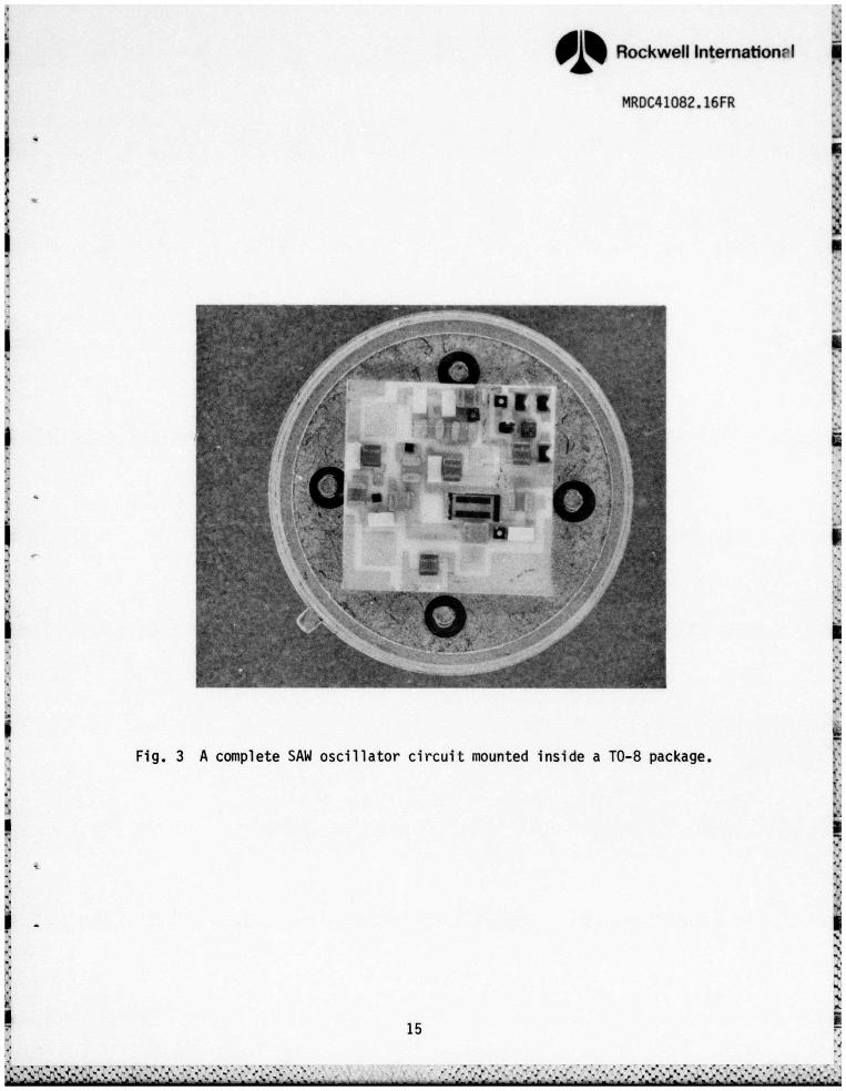
To minimize interaction from the other circuit components, we prefer
that the SAW device be separately packaged in its own hermetically sealed .
enclosure. Figure 3 shows a typical impedance-matched SAW package which is
connected to the remainder of the oscillator circuitry through impedance-
matched microstrip lines.
14C7324A/sn
-j -..--.

7-. 75
Rockwell International
MRDC41082.16FR
5.0 TECHNICAL APPROACH
5.1 Cantilever Beam Design
For preliminary design analysis, the objectives are to determine the
important performance characteristics and design parameters, and to get a
rough idea of their expected ranges. Thus, we consider just the simplified
design shown in Fig. 4, which shows a simple, rectangular solid beam of length
L, breadth b and height h clamped at one end. The free end is loaded by a
proof mass of diameter d. The important performance characteristics of this
device are the "detection threshold" ad and the lowest natural resonant fre-
quency fn" Let us assume that the proof mass is made of invar, which has a3density of 8 g/cm 3 . Therefore, the proof mass will be:
m = 8% (d/2)2b (1)
The natural resonant frequency of the beam will then be the following:
(2nf )2 bh 3 E (2)4mL
where E is Young's modulus for the beam material (quartz). Using Eqs. (1) and
(2), the following formula for the diameter of the proof mass can be derived:
d [Eh 3 /(8nL 3 (3/2"d- 2itf (3)n
Assuming a constant minimum natural frequency of 200 Hz, a family of curves of
beam thickness as a function of beam length is shown in Fig. 5. In this plot,
the diameter of the proof mass is chosen as a step variable.
16C7324A/sn
,-' .-,- ". -".-". ".- .".-.-.".-".-.- .- "- 2-.'>)". "- .' . ".-"...-".-.-."..'..".-'-...-".."..-.........""....."..--.....-.--.• ..----...,-....-'..-

Rockwell International
MRDC41082.16FR
Clamped end(Attached to vehicle frame)
Input
Fig esin shemti ofa SW cntiev Remsensor
17
C7324A/sn
7-

j Ei~ Rockwell International
* MRDC41O82 .16FR
Fn=200 Hz, d stepped
-
z
0 <)3
00
LOG(BEAM LENGTH) (CM)Od=.OO1 cm Ad=.O1 cm OZd=.l cm Xd=1 cm +d=10 cm
Fig. 5 Beam thickness as a function of beam length for proposed proof mass.Minimum natural frequency is 200 Hz.
C7324A/sn

1%
, Rockwell International
MRDC41082.16FR
To derive a relation for minimum detectable acceleration of the beam
as a function of the beam dimensions, we will consider our current frequency
noise floor" of 10-10 stability. These data are already reported and corres-
pond to a minimum detectable strain of about 10-10 parts/part. The strain at IF.
the surface of the beam at the beam "root" is related to the acceleration by
the following formula:
6Lma (4)
Ebh
Combining Eqs. (1) to (4), the minimum detectable acceleration can be derived:
ad : 0 2(2nfn)2 L2 (5)d 3h
Assuming a constant minimum natural frequency of 200 Hz, a family of curves of
beam thickness as a function of beam length shown in Fig. 6. In this plot,
the minimum detectable acc;leration ad is chosen as a step variable in the
unit of Gs.
5.2 Design of SAW Resonators
A SAW resonator is the actijal sensor in SAW accelerometer. A set of
the masks has been designed for the SAW resonator at 350 MHz range. Figure 7
shows the superimposed boundary patterns of the three masks required for the
resonator. The resonator device has a size of 4 x 7 mm and a line resolution
of 2 &ro.
To simulate a substrate resonator, an equivalent circuit like the one
shown in Fig. 8 is used. Elements of both circuits are quite similar, with
Cr, Lr and Rr as resonant elements. C. is the static capacitance of the IDT
. where R and L are the parasitic resistance and parasitic conductances,s" .
respectively. Using the equivalent circuit model, the amplitude and phase - -
response of the designed resonator are shown in Fig. 9.
19C7324A/sn

SRockwell International p
01
MRDC41O82. 16FR
Fn=200, Am, stepped
0-
E -
-3-
Ui -4 2r-z
-5
0
-J-7-
-8
-10--1 0
LOG(BEAM LENGTH) (mO]Am=10 -6 G AAm=10 -4 G *Am=10 -2 G XAmn=1 G
Fig. 6 Design tradeoff for SAW accelerometer with natural frequency at200 Hz.
20C7324A/sn

7- . - .. -. m
0 % Rockwell International
MRDC41O82. 16FRI~Ln
LiO0 Ok
C1 LLL
z
00
LO LCm
4-,
N
oo
L ..
.
n a) a)
21iC732Lrrs

Rockwell International
MRDC41082. 16FR
.F1
0-0
IbI%
Fig 8Eqivlen crcit fo SW esnatr:(a mdelfo oe-orresoator (bmodl fo tw-por resnatR
r..
C~rA
I(a
22rC72As
0 . .

Oik Rockwell International PL
MRDC41O82.16FR__
-5 5
-15
45-25
S-30~-35 LI -
Ll -45
-55 Xn-so
~-65--- 5
.5' -75
-05
3N6 325 356 375 isa
FREQUENCY -MHz
*Fig. 9 Theoretical simulation of complex return loss of the resonatordesigned for the SAW accelerometer.
23C7324A/sn
O Rockwell International
MRDC41082.16FR
5.3 Silicon Accelerometer
Figure 10 is a photograph of typical Si accelerometer chips, where
one chip is mounted inside a TO-8 package with wire bonds to the device con-
tacts. Shown in Fig. 11 is a more detailed microphotograph of the chip. The
-. monolithic accelerometer is an IC containing an acceleration sensor. The
acceleration sensor consists of a miniature cantilever beam containing a thin-
film piezoelectric capacitor on top. This beam is etched out of a part of the
*Si "chip" using advanced etching techniques. Acceleration forces normal to
the surface of the chip cause the beam to bend, and this induces strain in the
piezoelectric capacitor. The piezoelectric effect converts this strain into
an electrical charge which is proportional the the acceleration. The charge
is stored in the capacitor, so that the electrical potential at the output of
the capacitor is again proportional to acceleration. The electrical signal is
buffered by an on-chip PMOS transistor, which prevents the charge from leaking
to ground. The on-chip IC also includes a temperature-compensating capacitor
to cancel pyroelectric effects.
The monolithic acceleroneter has the essential military requirements
of small size, low weight and low power consumption. It uses the low-cost t
photolithographic fabrication methods developed for the IC industry.
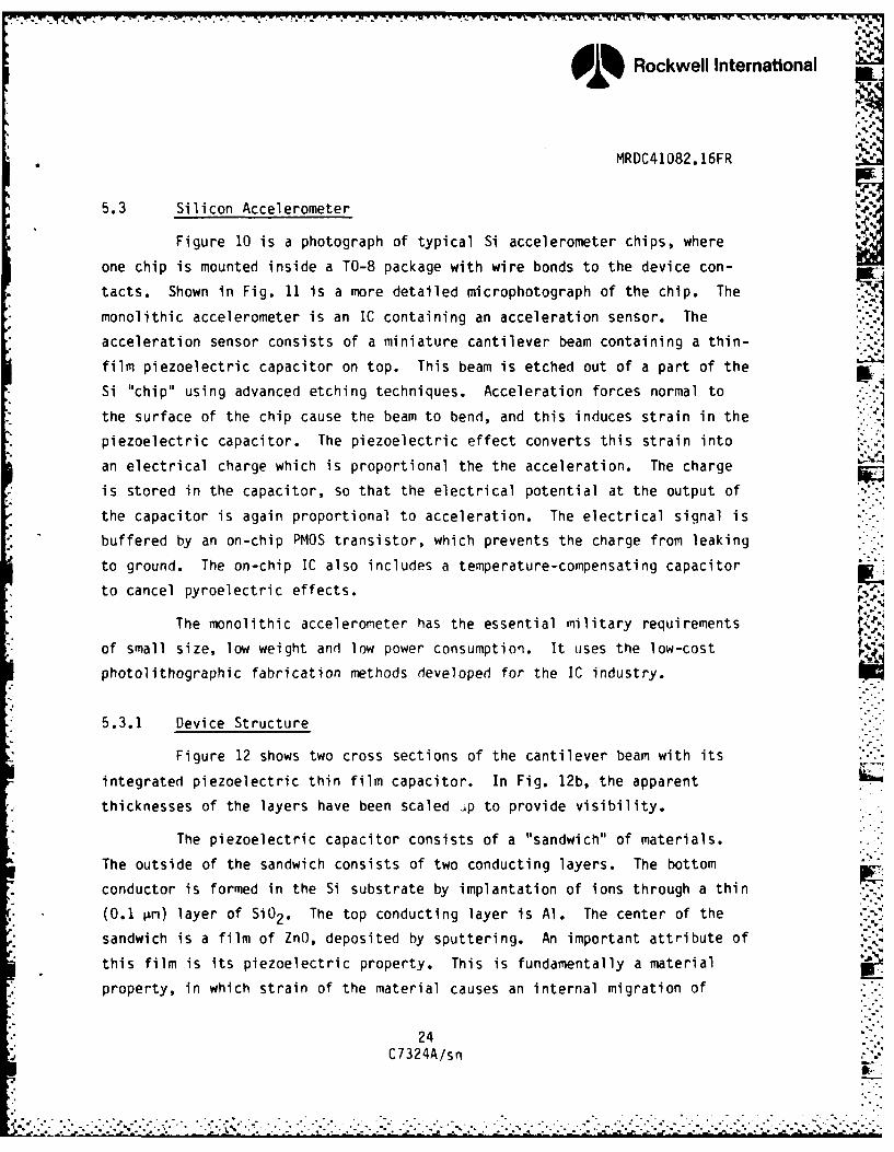
5.3.1 Device Structure
Figure 12 shows two cross sections of the cantilever beam with its
integrated piezoelectric thin film capacitor. In Fig. 12b, the apparent
thicknesses of the layers have been scaled ip to provide visibility.
The piezoelectric capacitor consists of a "sandwich" of materials.
The outside of the sandwich consists of two conducting layers. The bottom
conductor is formed in the Si substrate by implantation of ions through a thin
(0.1 Lm) layer of Si0 2 . The top conducting layer is Al. The center of the
sandwich is a film of ZnO, deposited by sputtering. An important attribute ofthis film is its piezoelectric property. This is fundamentally a materialproperty, in which strain of the material causes an internal migration of
24C7324A/sn
° . * ** . . *** . *


Oi% Rockwell International
MRDC41O82 .16FR
CANTILEVER BERM
I I
(a)
SPUTTERED SiO2
THERMA SiO2IZINC OXIDE
SILICON
(b)
* Fig. 12 Detailed structure of a Si cantilever heam sensor: (a) cross sectionof beam; (b) scale-up cross section for clarity.
27C 732 4AIs n

, , -' ,"
. " _'. "- " - - " * . "- - 11 - * - -. -. - l - - - W --
Rockwell International
MRDC41082.16FR
electrostatic charge. The direction of this charge migration depends on the '"
orientation of the crystallographic axes of the material, which must be con-trolled in the film.
In the Rockwell laboratory, ZnO is used as a piezoelectric film. ZnO
has hexogonal crystal symmetry and pyroelectric sensitivity. The pyroelectric
effect is one in which a change in temperature of the material causes the same
sort of charge transfer as the piezoelectric capacitor. To eliminate sensi-
tivity of the output bias of the monolithic accelerometer to temperature, a
compensated capacitor is designed as part of sensor.
The piezoelectric capacitor is only a part of the IC that is designed
into the monolithic accelerometer. The schematic circuit diagram in Fig. 13
. shows two piezoelectric capacitors designed to cancel out the pyroelectric
"* effect. (The piezoelectric capacitors are represented by capacitor symbols,
with a shaded region on one electrode.) These piezoelectric capacitors are
identically fabricated and connected in series, but back-to-back. In this
configuration, the net output signal change due to a common temperature change
is cancelled. However, if only one of these capacitors is on the cantilever
bean, the signal due to the strain input (shown by the wriggly arrow) will
appear at the PMOS gate. The PMOS gate isolates the capacitor circuit from
ground, so that the stored charge (representing the input acceleration) does
not decay over time. The degree of isolation was verified experimentally by
; straining the piezoelectric capacitor and by observing the PMOS output over a
period of 24 h, then by releasing the strain and observing the PMOS output
signal. The estimated decay time constant from this experiment was several
days.
5.4 Guidance System Simulation
The SAW resonator has a frequency stability of one port in 1010.
* This number is comparable to that of the bulk wave crystal oscillators. Since
*, the frequency counting is gated in a short time (1 to 60 s), the value of 1011)
* stability should be referred to as short-term frequency stability. The SAW
28C7324A/sn
"'.- . _-, . ._ -. . ,J -_. . - - . --. . -', '. ,- -_ ._. ..... ._. _.-..:i .. - ,.:i ;. , . .... -, ' : - '; - -,-'''; ' ' , .'''.. ' .'.. _.'z "- ., I ,

Rockwell International ~
MR0C41082. 16FR 5
-4-)=C
CLL
29~
C7324A/L

Rockwell International
MRDC41082.16FR
resonator is a strain sensor; therefore, substrate material is contributing
predominately to the device performance. Considering the temperature-stabil-
ity requirement for some tactical missile applications, quartz substrate is
chosen for the SAW resonator. Special orientation of quartz has temperature
characteristics necessary to make temperature compensated*SAW accelerometers.
Since the maximum allowable material strain for quartz is 200 ppm,
for working at 10 Gs acceleration input, the device performs on scale factor
of 20 ppm/G. Using these data, both bit quantization and frequency scale
factor can be determined.
1. Bit quantization is defined as the smallest detectable velocity at
the maximum acceleration input. Considering a center frequency of
376 MHz for the SAW resonator, the bit quantization of 1.3 x 10- 3 m/s
is achievable.
2. Frequency scale factor is defined, a count number of bits which is
equivalent to the unit of the acceleration. Considering a center
frequency of 376 MHz for the SAW resonator, a frequency scale factor
of 769 Hz/m/s 2 has been achieved.
Shown in Fig. 14 is the actual count output of a SAW sensor when mea-
sured by a counter with a 1 s gate time. The difference frequency of 60 KHz
has been subtracted, and only the deviation in the difference frequency
( 1 Hz) is shown. Summing the counts results in the velocity count (± 10 Hz)
as a function of time shown. This curve represents the area under the accel-
eration-frequency curve. Performing another summation as a function of time
results in the curve for displacement (t 4,000 Hz). The integrated velocity
error for the 1,000 s time period shown typically was less than 0.013 m/s, and
the position error typically was less than 5.2 m. As expected, the integrated
error is closely related to the integration time, and this is dependent on the
actual mission time or time for which no other guidance data are available.
30C7324A/sn
o. . - . . .

Oi% Rockwell International
MRDC41O82. 16FR
1.0
0.8
0.6
0.4
0 0.2
0 0
> 0.20 Frequency
-0.4
-0.6
Acceleration ±1 Hz-0.8 Velocity ±10 Hz -Sec
1.tPosition ±4,000 Hz - Sec2
Time -9.
Fig. 14 Measured count output of a SAW dual crystal sensor vs time. Totaltime was approximately 18 min with a 2 s gate time. Also shown isthe computed velocity from integrating once, as well as thedisplacement as a result of integrating the counter output twice.
31C7324A/sn

Rockwell International
MRDC41082.16FR
6.0 RESULTS
6.1 Fabrication of SAW Resonators
The SAW resonator starting material is a Y-cut, single crystal quartz
with an ultra-fine polish on one surface. Typically, the RMS surface rough-
ness is less than 5UA. After the metal electrode pattern has been defined,
the metal thickness is evaluated for the desired value, as well as a check of
metal thickness uniformity. Uniformity of the deposited metal thickness is
important to achieving resonators closely matched in frequency. An RF probing
technique was used to measure the RF frequency prior to any other processing
of the wafers. For example, the frequency sensitivity of Al electrode thick-
ness was typically 1.67 KHz/A at a nominal 350 MHz resonator. Maintaining a
deposition uniformity of less than 5% is necessary to achieve devices with
less than 200 ppm frequency variation.
To achieve high Q in SAW resonators, efficient surface wave reflec-
tion in the grating regios of the resonator must occur. This is done by pho-
tolithographically defining patterns on the wafers such that windows are
opened in the reflecting grating regions of the resonator. The reflecting
grating regions of the resonator are then ion-etched using a CF4 and oxygen
mixture. The photoresist prevented etching of any of the transducer regions,
and the Al in the grating regions acted as an etch mask, so that only the
quartz between the grating was etched. The etching produces grooves between
the reflector structure electrodes. The etching enhances the surface wave re-
flection at the grooves, and also lowers the resonant frequency of the grat-
ings to coincide with the transducer frequency. This dispersion was accounted
for in the original mask design with different periodicity between the grat-
ings and the transducer. After plasma etching, the resist is removed and the
resonators are pretested using an RF probe.
After pretesting, the wafers are diced and mounted. For the purpose
of the aging testing program, the dicing format yields two resonators on the =
same chip. This structure is termed "dual crystal" and has been used exten-
32C7324A/sn
I ., ,a. . ' -L .t ' _ ._ . .' . , -' -' . " . .. . . . " . . .. ' . '. .. .• . " . . .' . - .'.d
j Rockwell International
MRDC41082.16FR
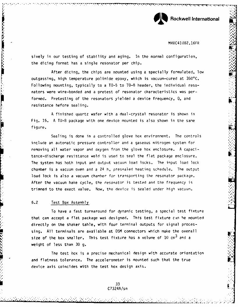
sively in our testing of stability and aging. In the normal configuration,
the dicing format has a single resonator per chip.
After dicing, the chips are mounted using a specially formulated, low
outgassing, high temperature polimide epoxy, which is vacuum-cured at 350'C.
Following mounting, typically to a TO-5 to TO-8 header, the individual reso-
nators were wire-bonded and a pretest of resonator characteristics was per-
formed. Pretesting of the resonators yielded a device frequency, Q, and
resistance before sealing.
A finished quartz wafer with a dual-crystal resonator is shown in
Fig. 15. A TO-8 package with one device mounted is also shown in the same
figure.
Sealing is done in a controlled glove box environment. The controls
include an automatic pressure controller and a gaseous nitrogen system for
removing all water vapor and oxygen from the glove box enclosure. A capaci-
tance-discharge resistance weld is used to seal the flat package enclosure. -
The system has both input and output vacuum load locks. The input load lock
chamber is a vacuum oven and a 24 h, presealed heating schedule. The output
load lock is also a vacuum chamber for transporting the resonator package.
After the vacuum bake cycle, the resonator is tested and the frequency is
trimmed to the exact value. Now, the device is sealed under high vacuum.
6.2 Test Box Assemhly
To have a fast turnaround for dynamic testing, a special test fixture
that can accept a flat package was designed. This test fixture cin be mounted
directly on the shaker table, with four terminal outputs for signal proces-
sing. All terminals are available at OSM connectors which make the overall
size of the box smaller. This test fixture has a volume of 10 cm3 and a
weight of less than 30 g.
The test box is a precise mechanical design with accurate orientation
and flatness tolerance. The accelerometer is mounted such that the true
device axis coincides with the test box design axis.
33C7324A/sn


Rockwell International
MRDC41082.16FR
One important characteristic of the test box is the ability of multi-axis testing. To demonstrate the multi-axis experiment, we designed a special
test nox for vertically mounted and 45*-rotated Z-axis mounted accelerometers.
To mount the accelerometer chip inside the flat package parallel to the test
. box, a special alignment technique is used to make the beam parallel to the
". package.
To analyze the data, a mathematical model for the operation of threeorthogonally mounted accelerometer devices will be developed. The empirical
data will be compared with the mathematical model to determine the degree of
conformance of the empirical data with the theory. From the results of both
the measurements and the mathematical model, scale-factor accuracy and
linearity of three-axis accelerometers can be determined.
6.3 Dynamic Testing
For exact device characterization, a complete series of measurements
must be made under varying acceleration conditions, so that a meaningful
three-axis characterization and a correct algorithm, including all of the
effects of cross-coupling, can be derived. When the acceleration is not in
line with the design axis, the x, y and z components of acceleration must be
taken into account in determining the response of the device.
By careful fixture design and mounting, these off-axis components can
be evaluated in the single device through a series of accelerometer tests with
variable input axes to the accelerometer device. The nature and magnitude of
the cross-coupling, three-axis measurements on a single device will first be
carefully evaluated to better understand single device characteristics.
Based on the results of this kind of test, three accelerometers will
be mounted in the three-axis planes of a test box and simultaneous data will
be taken. This fixture will then be evaluated at various acceleration angles
and magnitudes while maintaining separate data channels for each device.
Thus, an empirical assessment of the three-axis performance of the monolithic
accelerometer can be accomplished. The multi-axis measurement is a powerful
35C7324A/sn

:.. .j - - *-- -. .J -; -- -- ~ . . . r - -
Rockwell International
MRDC41082.16FR
technique for characterizing the cross-axis error presented in most navigation
systems. -'h
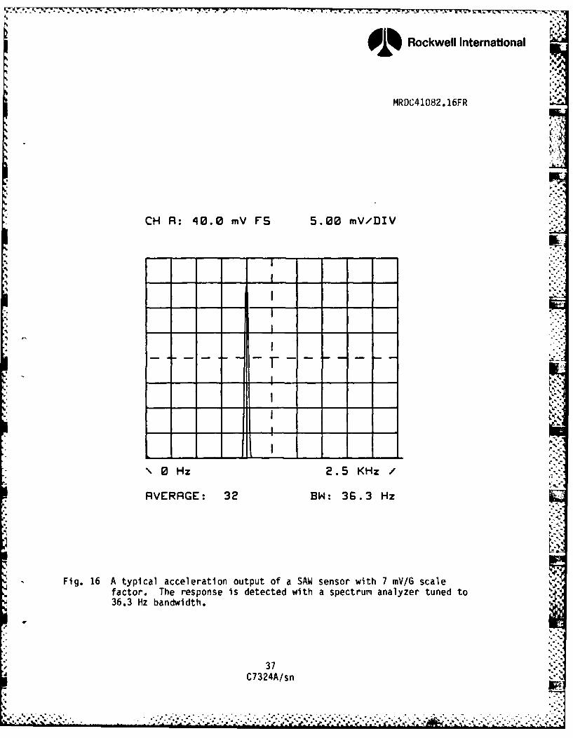
Figure 16 shows a typical output response of the accelerometer at
5 Gs and 100 Hz, which is the result of a single axis measurement. For this
measurement, the spectrum analyzer was set to a 36.3 Hz bandwidth and the
device shows a scale factor of 7 mV/g.
The results of typical cross-axis data are shown in Fig. 17. The
response shown in the figure is when the accelerometer is mounted vertically.
In this case, the cross-axis signal is visible at 200 Hz and 5 G. For
comparison, the same device was mounted horizontally with designed axis, and
the data were taken in the identical test parameter. The results are shown in
Fig. 18.
36C7324A/sn
. . . . . . . . . . . . . . . . . . . . . . . . . . . .
. . . .. . *
OiRockwell International
MRDC41O82.16FR
CH A: 40.0 mV FS 5.00 MV/DIV
0 z2. 1
36.3 2.5 bandidth
AVERAGE 32C73238.3 H

4% -F
Rockwell International
01% WI
MR0C41082.16FR .
CH R: 400 uV FS 50.0 uv/DIV
\OHz 5 KHz/PERK: 153EP-105 M-RXES DRTR TIC
* Fig. 17 A typical cross-axis response of a SAW accelerometer sensor at2000 Hz.
IWN
38C7324A/sn

"-W ~ ~ -so -. vTW,
Rockwell Internationaloi9
.1'
MRDC41U82.16FR
.1
CH R: 400 uV FS 50.0 uV/DIV '1
- -- o%-
<............
0 Hz 5 KHz/PER~K: 165 Bkd: 30.0 HzEP-105 M-RXES ORTR HIC
* Fig. 18 A typical true-axis response of a SAW accelerometer sensor at2000 Hz.
39C7324A/sn
..............................................................

.W -.- - -. Y-0l r 7.
E Rockwell International
MRDC41082.16FR
* 7.0 FUTURE PLANS
The results of this program established a complete SAW sensor fabri-
cated on a quartz substrate. The device showed high short-term stability and
excellent frequency scale factor. During the term of this work, we were not
able to make a prototype accelerometer with the proposed requirement. The
following tasks should be accomplished for the required accelerometer.
1. For the highly sensitive accelerometer, the quartz cantilever beam
should have a hammer-head shape. Our study showed that a two-
dimensional shape is practical, but is not adequate to produce enough
sensitivity. Therefore, a three-dimensional quartz cantilever beam
should be studied.
2. For the requirement in frequency stability, device packaging should
be investigated. This study has already started under this program,
but it is necessary to continue the research for a better solution.
3. A complimentary technique using a Si-based accelerometer should be
studied for the purpose of fast reaction time devices. This phase
was also initiated under the present contract, but needs more
investigation.
40C7324A/sn

Rockwell International
MRDC41O82.16FR
8.0 REFERENCES
1. M.E. Motamedi and A.P. Andrews, "Monolithic Accelerometer," Final
Report, Contract No. DASG6O-83-C-0101, June 1985.
2. W.E. Rosvold and M.L. Stephens, "Cantilever Accelerometer," AFAL-TR-
77-152, WPAFB, OH, 1977.
3. M.E. Motaniedi, "Passivation on High-Q Acoustic Strain Sensors for
Accelerometer," Final Technical Report, Contract No. F49620-82-C-
0012, November 1984.
44
C7324A/sn

, Rockwell International
MRDC41082.16FR
APPENDIX A: RESEARCH FACILTIES
Facilities offer 10K sq ft of class 10,000, with class 100 working
areas for wafer processing and 5K class 30,000 area for assembly process line.
The areas involved are secured for classified material. Facility capabilities
include MIL-M38510 compliance, MIL-Q-9858 quality system, MIL-STD-883 screen-
ing and burn-in, and MIL-C:45662 traceability and calibration. The assembly
process line has a packaging capability of 5,000 per week for a variety of UK
different package types such as ceramic hermetic, dips, flatpacks, LLCC and
LCC. A number of aligners are currently in use. The Perkin Elmer projection
aligners, GCA-MANN 4800 DSW and Cannon 4X projection aligner are among these.
Also, a new Censor SRA-100 automatic step-and-repeat projection aligner (Fig.
A.1) has been purchased recently and is now in use at the MRDC Thousand Oaks
facility. A Jade step-and-repeat projection aligner is now being used exclu-
sively for DSW and mask processing of SAW devices (Fig. A.2). For high reso-
lution lithography, a Cambridge MF-6 electron beam system is being used at the
same facility. The pattern generator tapes for mask production are made using
the Calma GDS11 CAD system. Recently, a second color terminal which greatly
enhances the turnaround time has been added to the system.
A HP8510 network analyzer is used in conjunction with a HP9836 com-
puter for automated measurements involving SAW devices (Fig. A.3). The HP8510
is the most advanced network analyzer available at the present time. The sys-
tem is equipped with the time-domain measurement and phase-locked system.
Test systems such as the Tektronix 3260 (wafer probe, package test,
environmental characerization), Accutest 7900 (50 MHz, 60 dual I/O channels,
temperature testing) are being used routinely for testing and characterization
at the center. A CVD reactor for Si3N4 and dry etching of Si and oxide (Fig.
A.4) and an RF sputtering system for deposition of ZnO films (Fig. A.5) are
also being used in SAW processing.
44
42 .-
C7324A/sn
.- '. o ..- .......-. . ", .° 4 . . ". ° •.4.. ". o . " - , . - . , •. , . ..... . . . .* . "


