05 digital cmos ic design - universiti tunku abdul rahmanstaff.utar.edu.my/limsk/integrated circuit...
TRANSCRIPT

Chapter 5 UEEA2223/UEEG4223
Integrated Circuit Design
Digital CMOS IC Design


Prepared by Dr. Lim Soo King 20 Jan 2011.

- i -
Chapter 5 Digital CMOS IC Design ..............................................137 5.0 Introduction ............................................................................................ 137 5.1 Transistor Level Design of Logic Gate ... Error! Bookmark not defined. 5.2 Transistor Level Design of CMOS Complex Logic Circuit ......... Error! Bookmark not defined. 5.3 Pass-Transistor ......................................... Error! Bookmark not defined.
5.3.1 n-channel MOS Pass-Transistor ....................... Error! Bookmark not defined. 5.3.1.1 Pass Logic 1 ....................................................................... Error! Bookmark not defined. 5.3.1.2 Pass Logic 0 ....................................................................... Error! Bookmark not defined. 5.3.1.3 Switching Time .................................................................. Error! Bookmark not defined.
5.3.2 p-channel MOS Pass-Transistor ....................... Error! Bookmark not defined. 5.3.2.1 Pass Logic 1 ....................................................................... Error! Bookmark not defined. 5.3.2.2 Pass Logic 0 ....................................................................... Error! Bookmark not defined. 5.3.2.3 Switching Time .................................................................. Error! Bookmark not defined.
5.3.3 Series Connected Pass-Transistor ..................... Error! Bookmark not defined. 5.3.4 Application of Pass-Transistor .......................... Error! Bookmark not defined.
5.4 Pseudo n-MOS Logic Gate ...................... Error! Bookmark not defined. 5.5 Transmission Gate ................................... Error! Bookmark not defined.
5.5.1 Electrical Characteristics ................................... Error! Bookmark not defined. 5.5.1.1 Transfer Logic 1 ................................................................ Error! Bookmark not defined. 5.5.1.2 Transfer Logic 0 ................................................................ Error! Bookmark not defined.
5.5.2 RC Model of Transmission Gate ....................... Error! Bookmark not defined. 5.5.3 Application of Transmission Gate .................... Error! Bookmark not defined.
5.6 Domino Logic Circuit .............................. Error! Bookmark not defined. 5.7 Transistor Level Design of Flip-Flop ..... Error! Bookmark not defined. 5.8 Random Access Memory Devices ........... Error! Bookmark not defined.
5.8.1 RAM Memory Cell ............................................. Error! Bookmark not defined. 5.8.1.1 Six-Transistor Static Memory Cell .................................. Error! Bookmark not defined. 5.8.1.2 Three-Transistor Dynamic Memory Cell ....................... Error! Bookmark not defined. 5.8.1.3 One-Transistor Dynamic Memory Cell .......................... Error! Bookmark not defined.
5.9 dc Characteristic of a NOT Gate ............ Error! Bookmark not defined. 5.10 Electrical Analysis of NAND Gate ........ Error! Bookmark not defined. 5.11 Electrical Analysis of NOR Gate .......... Error! Bookmark not defined. 5.12 Power Dissipation of NOT Gate ........... Error! Bookmark not defined. Exercises .......................................................... Error! Bookmark not defined. Bibliography ................................................................................................. 212
- ii -
Figure 5.1: The CMOS circuit of a NOT gate .................... Error! Bookmark not defined. Figure 5.2: Layout of NOT gate ......................................... Error! Bookmark not defined. Figure 5.3: CMOS circuit of a NOR gate ........................... Error! Bookmark not defined. Figure 5.4: The layout of a 2-input NOR gate.................... Error! Bookmark not defined. Figure 5.5: 8-MOS transistor design of an OR gate ........... Error! Bookmark not defined. Figure 5.6: CMOS circuit of an OR gate ............................ Error! Bookmark not defined. Figure 5.7: CMOS circuit of a NAND gate ........................ Error! Bookmark not defined. Figure 5.8: The layout of a 2-input NAND gate ................ Error! Bookmark not defined. Figure 5.9: CMOS circuit of an AND gate......................... Error! Bookmark not defined. Figure 5.10: CMOS circuit of Boolean function f(A, B, C) = )CB(A +⋅ Error! Bookmark
not defined. Figure 5.11: VLSI layout of the Boolean function f(A, B, C) = )CB(A +⋅ ................ Error!
Bookmark not defined. Figure 5.12: CMOS circuit of an exclusive OR gate............ Error! Bookmark not defined. Figure 5.13: Pseudo n-MOS transistor circuit of carry out portion of a full adder ....... Error!
Bookmark not defined. Figure 5.14: Pseudo n-MOS transistor circuit of sum portion of a full adder ............... Error!
Bookmark not defined. Figure 5.15: n-channel MOS transistor pass-transistor ........ Error! Bookmark not defined. Figure 5.16: p-channel MOS transistor pass-transistor ........ Error! Bookmark not defined. Figure 5.17: A series-connected n-channel pass-transistor .. Error! Bookmark not defined. Figure 5.18: Dual threshold-loss n-channel pass-transistor . Error! Bookmark not defined. Figure 5.19: Exclusive NOR gate design using n-channel pass-transistor Error! Bookmark
not defined. Figure 5.20: Exclusive NOR gate design using p-channel and n-channel pass-transistors
.......................................................................... Error! Bookmark not defined. Figure 5.21: 2-input AND gate design using p-channel and n-channel pass-transistors
.......................................................................... Error! Bookmark not defined. Figure 5.22: 3-input AND gate design using p-channel and n-channel pass-transistors
.......................................................................... Error! Bookmark not defined. Figure 5.23: (a) A pseudo n-MOS inverter and (b) The voltage transfer characteristic of the
inverter ............................................................. Error! Bookmark not defined. Figure 5.24: Layout of a complex logic function C)BA( +• designed with pseudo n-MOS
gate design concept .......................................... Error! Bookmark not defined. Figure 5.25: The block diagram of a PLA ............................ Error! Bookmark not defined. Figure 5.26: The design of logic circuit using PLA ............. Error! Bookmark not defined. Figure 5.27: CMOS transmission gate ................................. Error! Bookmark not defined. Figure 5.28: The condition of transmission gate for input X = VDD ... Error! Bookmark not
defined. Figure 5.29: The Mode condition of n-MOS and p-MOS transistors during output transition
from logic 0 to logic 1 ...................................... Error! Bookmark not defined. Figure 5.30: The condition of transmission gate for input X = 0 V ...... Error! Bookmark not
defined. Figure 5.31: The Mode condition of n-MOS and p-MOS transistors during output transition
from logic 1 to logic 0 ...................................... Error! Bookmark not defined. Figure 5.32: RC model of a transmission gate with input node X and output node Y.. Error!
Bookmark not defined.

- iii -
Figure 5.33: The RTG of a transmission gate with logic 1 transfer ...... Error! Bookmark not defined.
Figure 5.34: The RTG of a transmission gate with logic 0 transfer ...... Error! Bookmark not defined.
Figure 5.35: A 2-to-1 multiplexer circuit ............................. Error! Bookmark not defined. Figure 5.36: CMOS circuit of a 2-input exclusive-NOR gate ............. Error! Bookmark not
defined. Figure 5.37: CMOS circuit of an exclusive OR gate utilizing transmission gate ......... Error!
Bookmark not defined. Figure 5.38: CMOS OR gate designed with transmission gate ........... Error! Bookmark not
defined. Figure 5.39: CMOS AND gate designed with transmission gate ........ Error! Bookmark not
defined. Figure 5.40: General circuit of domino circuit design ......... Error! Bookmark not defined. Figure 5.41: Domino circuit of a 3-input OR gate ............... Error! Bookmark not defined. Figure 5.42: A domino 3-input OR gate with charge keeper p-MOS transistor ........... Error!
Bookmark not defined. Figure 5.43: Domino circuit of a 3-input OR gate with feedback control to charge keeper p-
MOS transistor ................................................. Error! Bookmark not defined. Figure 5.44: A domino 3-input OR gate with inverter feedback to charge keeper p-MOS
transistor ........................................................... Error! Bookmark not defined. Figure 5.45: A basic bi-stable element ................................... Error! Bookmark not defined. Figure 5.46: CMOS circuit of a bi-stable element .................. Error! Bookmark not defined. Figure 5.48: The layout of the bi-stable element .................... Error! Bookmark not defined. Figure 5.49: SR flip-flop ......................................................... Error! Bookmark not defined. Figure 5.50: CMOS circuit of a SR flip-flop .......................... Error! Bookmark not defined. Figure 5.51: A D flip-flop ....................................................... Error! Bookmark not defined. Figure 5.52: CMOS circuit of a D flip-flop ............................ Error! Bookmark not defined. Figure 5.53: Transmission gate design of a D flip-flop .......... Error! Bookmark not defined. Figure 5.54: Compact design of D flip-flop ........................... Error! Bookmark not defined. Figure 5.55: A master/slave D flip-flop .................................. Error! Bookmark not defined. Figure 5.56: Logic circuit of a JK flip-flop ............................ Error! Bookmark not defined. Figure 5.57: CMOS circuit design of a JK flip-flop ............... Error! Bookmark not defined. Figure 5.58: T flip-flop ........................................................... Error! Bookmark not defined. Figure 5.59: CMOS circuit design of a T flip-flop ................. Error! Bookmark not defined. Figure 5.60: Block diagram of a 1kx8 SRAM ........................ Error! Bookmark not defined. Figure 5.61: The six-transistor static RAM cell ..................... Error! Bookmark not defined. Figure 5.62: A three-transistor dynamic RAM cell ................ Error! Bookmark not defined. Figure 5.63: A 1-bit dynamic RAM cell ................................. Error! Bookmark not defined. Figure 5.64: The voltage bias condition of an inverter or NOT gate..... Error! Bookmark not
defined. Figure 5.65: The transient response of an inverter ................. Error! Bookmark not defined. Figure 5.66: The transistor level circuit of a NAND gate ...... Error! Bookmark not defined. Figure 5.67: Transition table and (b) condition of transistor of NAND gate .................. Error!
Bookmark not defined. Figure 5.68: NAND circuit for transient response calculation Error! Bookmark not defined. Figure 5.69: Transistor level design of a 2-input NOR gate ... Error! Bookmark not defined. Figure 5.70: (a) Transition table and (b) condition of transistor of NOR gate ................ Error!
Bookmark not defined.

- iv -
Figure 5.71: VTC plot of NOR gate, NAND gate and NOT gate ......... Error! Bookmark not defined.
Figure 5.72: NOR circuit for transient response calculation .. Error! Bookmark not defined. Figure 5.73: The drain current versus input voltage of the NOT gate at different mode of
operation .......................................................... Error! Bookmark not defined. Figure 5.74: Charging and discharging circuits of a NOT gate ............. Error! Bookmark not
defined.

- v -


- 137 -
Chapter 5
Digital CMOS IC Design
5.0 Introduction In the CMOS design, p-MOS and n-MOS transistor are used complimentary. P-MOS transistor is a logic 0 asserted high output device, which means that when p-MOS transistor is switched on with logic 0. According to the biasing condition of p-MOS transistor, the source voltage VS should be larger than drain voltage VD. Thus, the source of p-MOS transistor is usually connected to VDD power rail. Therefore, when the p-MOS transistor is switched on, the output will provide logic 1.
n-MOS transistor is a logic 1 asserted low output device. This shall mean
that logic 1 is used to switch on n-MOS transistor. According to the biasing condition of n-MOS transistor, drain voltage VD should be larger than source voltage VS. This shall mean logic 1 asserted low output transistor should be connected to ground rail or VSS rail. Thus, when the n-MOS transistor is switched on, the output will provide logic 0.
In this chapter, we shall discuss the transistor level design of logic circuit
and static combinational circuit. The chapter will cover the tri-state circuit. The designs using pseudo n-MOS transistor, pass-transistor and transmission gate are discussed in details. Other method for designing the logic circuit such as mirror logic circuit is discussed.
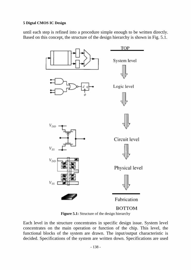
5.1 The Design Hierarchy
Integrated circuit can be complex like the microprocessor chip. Complete understanding of every aspect of the chip design and fabrication requires several years of study and practical experience. Designing an integrated circuit, which is general termed as chip, for a specific function, this chip is considered as a system. Hierarchical design approach is usually adopted in designing VLSI integrated circuit. This approach is also known as divide-and-conquer approach. This approach is commonly used in programming, whereby a procedure is written not as a huge list of primitive statement but as calls to simpler procedure. Each procedure breaks down the task into smaller operations
5 Digtal CMOS IC Design
- 138 -
until each step is refined into a procedure simple enough to be written directly. Based on this concept, the structure of the design hierarchy is shown in Fig. 5.1.
Figure 5.1: Structure of the design hierarchy
Each level in the structure concentrates in specific design issue. System level concentrates on the main operation or function of the chip. This level, the functional blocks of the system are drawn. The input/output characteristic is decided. Specifications of the system are written down. Specifications are used

5 Digtal CMOS IC Design
- 139 -
to create an abstract high level model. The abstract model contains information on the behavior of each block and the interaction among the block in the system.
Logic level is the level where logic network circuit of each functional
block is designed. At the end of design, a net list is generated that describes the logic gates and wire needed to implement the design.
Circuit design level is the step where logic network is transformed into
transistor as the switching devices. Digital variables are represented by voltage levels that change with time.
Once the circuit design is completed, it is transformed into a design file for
silicon integrated circuit physical design level. Physical design level involves transforming the electronic circuit into on-screen colored geometrical patterns using computer graphics and analysis tools. This step is also called the layout step.
The final step of the chip design is chip fabrication where physical integrated circuit is fabricated and put into package for eventual wiring into product used for application.
The approach is the top-down design approach. This is the appropriate way
for complex design such as microprocessor. Take for an example; the 64-bit processor cannot be designed bit by bit from the bottom-up approach. Small device is possible to be designed in this manner. However, for learning purpose, bottom-up design approach works well.
Hierarchical design approach helps the designer to organize the function of
a large number of transistors into particular, easy-to-summary function. The approach makes it easy to re-use pieces of chip, either by modifying an old design or to be used as a component for a new design.
5.2 Transistor Level Design of Logic Gate The Boolean function of the NOT gate is f(x) = X . According to Shannon’s expansion theorem, the Boolean function f(X) is f(X) = X•0 + X ⋅1. From the equation, one can see that there is logic 1 asserted low output and logic 0 asserted high output. Therefore, the design can be implemented with an n-MOS transistor for logic 1 asserted low output and a p-MOS transistor for logic 0 asserted high output. The CMOS circuit diagram of the NOT gate is shown in Fig. 5.2 and its corresponding layout is shown in Fig. 5.3.

5 Digtal CMOS IC Design
- 140 -
Figure 5.2: The CMOS circuit of a NOT gate
Figure 5.3: Layout of NOT gate
The Shannon’s expansion for a NOR gate is f(A, B) = 1BA •• + 0BA •• +
0BA ⋅⋅ + 0BA ⋅⋅ = ( )1BA ⋅⋅ + (A⋅0+B⋅0). Based on the criteria mentioned in earlier for the design of NOT gate, NOR gate can be designed with p-MOS transistors connected in series, which would be logic 0 asserted to get ANDed output logic 1 and two-n-MOS transistors connected in parallel, which would be logic 1 asserted to get Ored output logic 0. The CMOS circuit of a NOR gate is shown in Fig. 5.4 and its corresponding layout is shown in Fig. 5.5.

5 Digtal CMOS IC Design
- 141 -
Figure 5.4: CMOS circuit of a NOR gate
Figure 5.5: The layout of a 2-input NOR gate
The Shannon’s expansion for a OR gate is f(A, B) = 0BA ⋅⋅ + 1BA ⋅⋅ + 1BA ⋅⋅ +
1BA ⋅⋅ = ( )0BA ⋅⋅ + (A•1 + B•1). Based on the series, the design required logic 0 asserted low output and logic 1 asserted high output. This shall mean that to implement the function, beside the requirement of two n-MOS and two p-MOS transistors, it also requires two additional NOT gates. Thus, the total number of MOSFET transistor required is increased to eight, which are four n-MOS and

5 Digtal CMOS IC Design
- 142 -
four p-MOS transistors. The logic circuit of eight-transistor OR gate is shown in Fig. 5.6.
Figure 5.6: 8-MOS transistor design of an OR gate
The Boolean function for OR gate can be written as f(A, B) = ( )BA + , which shall mean that the function can be implemented with a NOR gate connected to a NOT gate. With this design, the number of MOS transistor required is six instead of eight mentioned earlier, which is shown in Fig. 5.7.
Figure 5.7: CMOS circuit of an OR gate

5 Digtal CMOS IC Design
- 143 -
The Shannon’s expansion for a NAND gate is f(A, B) = 1BA ⋅⋅ + 1BA ⋅⋅ + 1BA ⋅⋅ + 0BA ⋅⋅ = ( )1B1A ⋅+⋅ + (A⋅B⋅0). Based on the procedure mentioned in
earlier section for the design of NOR gate, the NAND gate can be designed with with p-MOS transistors connected in parallel, which would be logic 0 asserted to get Ored output logic 1 and two-n-MOS transistors connected in series, which would be logic 1 asserted to get ANDed output logic 0. The CMOS circuit of a NAND gate is shown in Fig. 5.8 and its corresponding layout is shown in Fig. 5.9.
Figure 5.8: CMOS circuit of a NAND gate
Figure 5.9: The layout of a 2-input NAND gate
5 Digtal CMOS IC Design
- 144 -
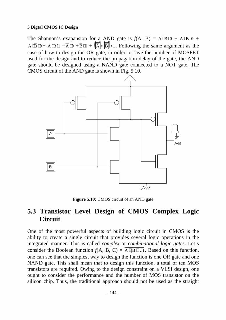
The Shannon’s exapansion for a AND gate is f(A, B) = 0BA ⋅⋅ + 0BA ⋅⋅ + 0BA ⋅⋅ + 1BA ⋅⋅ = 0A ⋅ + 0B ⋅ + [ ] [ ]( ) 1BA •• . Following the same argument as the
case of how to design the OR gate, in order to save the number of MOSFET used for the design and to reduce the propagation delay of the gate, the AND gate should be designed using a NAND gate connected to a NOT gate. The CMOS circuit of the AND gate is shown in Fig. 5.10.
Figure 5.10: CMOS circuit of an AND gate
5.3 Transistor Level Design of CMOS Complex Logic Circuit
One of the most powerful aspects of building logic circuit in CMOS is the ability to create a single circuit that provides several logic operations in the integrated manner. This is called complex or combinational logic gates. Let’s consider the Boolean function f(A, B, C) = )CB(A +⋅ . Based on this function, one can see that the simplest way to design the function is one OR gate and one NAND gate. This shall mean that to design this function, a total of ten MOS transistors are required. Owing to the design constraint on a VLSI design, one ought to consider the performance and the number of MOS transistor on the silicon chip. Thus, the traditional approach should not be used as the straight
5 Digtal CMOS IC Design
- 145 -
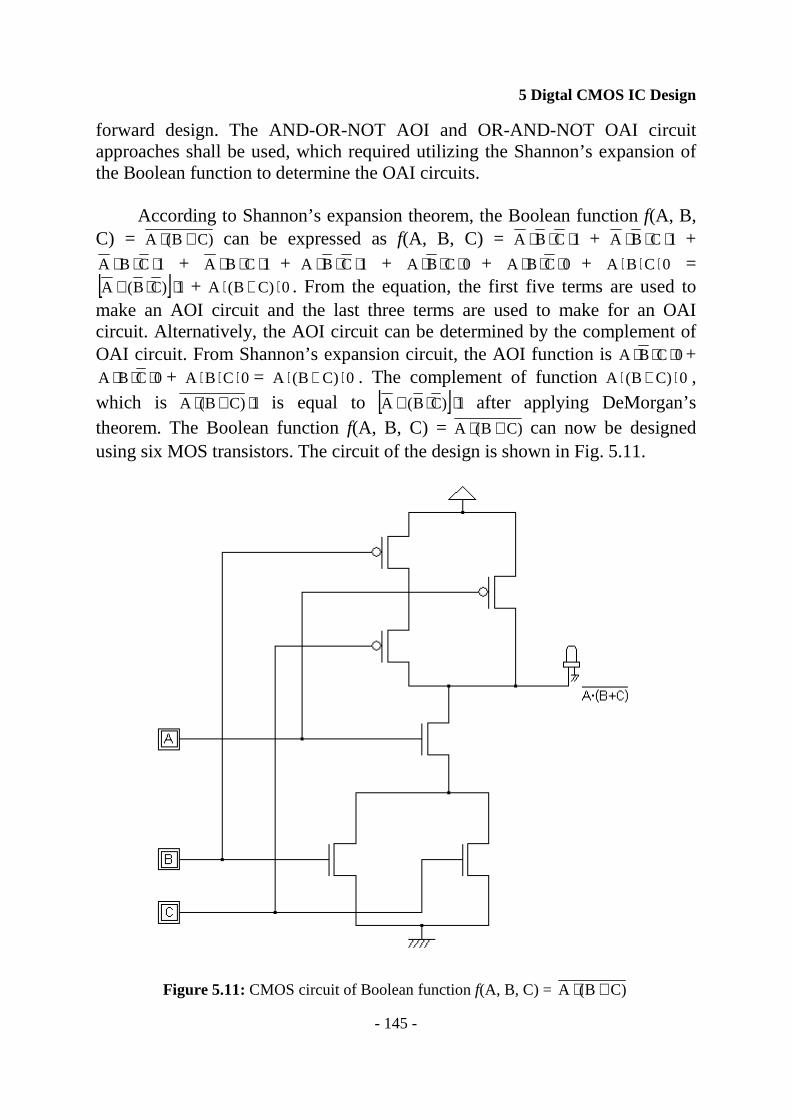
forward design. The AND-OR-NOT AOI and OR-AND-NOT OAI circuit approaches shall be used, which required utilizing the Shannon’s expansion of the Boolean function to determine the OAI circuits.
According to Shannon’s expansion theorem, the Boolean function f(A, B, C) = )CB(A +⋅ can be expressed as f(A, B, C) = 1CBA ⋅⋅⋅ + 1CBA ⋅⋅⋅ +
1CBA ⋅⋅⋅ + 1CBA ⋅⋅⋅ + 1CBA ⋅⋅⋅ + 0CBA ⋅⋅⋅ + 0CBA ⋅⋅⋅ + 0CBA ⋅⋅⋅ = [ ] 1)CB(A ⋅⋅+ + 0)CB(A ⋅+⋅ . From the equation, the first five terms are used to make an AOI circuit and the last three terms are used to make for an OAI circuit. Alternatively, the AOI circuit can be determined by the complement of OAI circuit. From Shannon’s expansion circuit, the AOI function is 0CBA ⋅⋅⋅ +
0CBA ⋅⋅⋅ + 0CBA ⋅⋅⋅ = 0)CB(A ⋅+⋅ . The complement of function 0)CB(A ⋅+⋅ , which is 1)CB(A ⋅+⋅ is equal to [ ] 1)CB(A ⋅⋅+ after applying DeMorgan’s theorem. The Boolean function f(A, B, C) = )CB(A +⋅ can now be designed using six MOS transistors. The circuit of the design is shown in Fig. 5.11.
Figure 5.11: CMOS circuit of Boolean function f(A, B, C) = )CB(A +⋅

5 Digtal CMOS IC Design
- 146 -
The layout of the function f(A, B, C) = )CB(A +⋅ is shown in Fig. 5.12.
Figure 5.12: VLSI layout of the Boolean function f(A, B, C) = )CB(A +⋅
The Boolean function of an exclusive OR gate is f(A, B) = A⊕B. The function can be re-written as BABABA)B,A( ⋅+⋅=⊕=f . Thus, the AOI for the n-MOS
transistor network is BABA ⋅+⋅ . Using pushing bubble technique, the p-MOS transistor OAI network is equal to )BA()BA( +⋅+ .
One would notice that the total number of MOS transistor required is twelve for the exclusive OR gate design shown in Fig. 5.13. However, the total number of MOS transistor can be reduced to a lesser number if pass-transistor, mirror logic circuit, pseudo n-MOS logic or transmission gates design approach are adopted.

5 Digtal CMOS IC Design
- 147 -
Figure 5.13: CMOS circuit of an exclusive OR gate
The Boolean function of a full adder is S = A⊕B⊕Ci and Co =
)CA()BA()CB( ii ⋅+⋅+⋅ = (A+B)⋅Ci +A⋅B, where S is the sum, Co is the carry-out, and Ci is the carry-in. The sum S is also equal to S = ( )CBA()CBA ii ⋅⋅+⋅⋅ +
)CBA()CBA( ii ⋅⋅+⋅⋅ , which can be expressed in terms of carry out Co equal to S = (A + B + Ci)⋅ iO CBAC ⋅⋅+ .
In order to save the number of MOS transistor used in the design, one of the methods is using pseudo n-MOS transistor circuit, which has carry-out Co circuit shown in Fig. 5.14. There is a total reduction of five p-MOS transistors. Student should attempt to design this CMOS version of the circuit. The designer has to take note the p-MOS transistor used in the pseudo n-MOS transistor design has to be sufficiently large enough to handle the current flow into the n-MOS transistor network and at the same time has sufficient worst case resistance for providing logic 0. Using circuit shown in Fig. 5.14, the worst case current drain in the n-MOS transistor network is the drain current of five n-MOS transistors simultaneously switched-on. Alternatively, the designer can design the circuit with four parallel standard p-MOS transistors.

5 Digtal CMOS IC Design
- 148 -
Figure 5.14: Pseudo n-MOS transistor circuit of carry out portion of a full adder
The similar approach can be used to design the sum part of the full adder. The pseudo n-MOS transistor version of the circuit is shown in Fig. 5.15. We shall discuss the physics of pseudo n-MOS transistor design in details in Section 5.5.
Figure 5.15: Pseudo n-MOS transistor circuit of sum portion of a full adder

5 Digtal CMOS IC Design
- 149 -
5.4 Pass-Transistor In this section, the characteristics of MOS transistor when the transistor is used as pass-transistor are analyzed. The study covers the transfer of voltage from source to drain and vice versa with the gate used as the control, and the application of pass-transistor for designing logic circuit. 5.4.1 n-channel MOS Pass-Transistor Let’s analyze the n-channel MOS pass-transistor shown in Figure 5.16. The input has a voltage and the output is connected to a capacitive load that has a voltage across it. The capacitor represents the total capacitance at the output node and has several contributions. Placing a logic 1 at the gate switches on the n-channel MOS transistor into conduction, connecting the input and output nodes.
Figure 5.16: n-channel MOS transistor pass-transistor
5.4.1.1 Pass Logic 1 Let’s analyze the circuit when a logic 1 is passed through this transistor. The gate-to-source voltage VGS is equal to VGS = VDD – Vout(t), whilst the drain-to-source voltage is VDS = VDD – Vout(t). Once can see that the transistor is in saturation mode. Thus, the drain-to-source current IDS is
IDS = ( )2tnoutDD
noutout V)t(VV
2dt
dVC −−
β= (5.1)
Integrating equation (5.1) with the condition at time t = 0 output voltage Vout(t) = 0V, the output voltage Vout(t) is found to be equal to

5 Digtal CMOS IC Design
- 150 -
Vout(t) = ( ))2/(t1
)2/(tVV
n
ntnDD τ+
τ− (5.2)
τn is the time constant which is equal to CoutRn = )VV(
C
tnDDn
out
−β. From equation
(5.2), it can be shown that the maximum output voltage Vout(max)(t) is equal to (VDD-Vtn) for time t →∞. Since the maximum output voltage for an n-channel MOS pass-transistor is VDD- Vtn, therefore, it is usually claimed that this type of pass-transistor passes a weak logic 1 and the loss of the output is said to be threshold voltage loss. It is obvious to maintain conduction, the gate-source voltage VGS must have a minimum value of Vtn. 5.4.1.2 Pass Logic 0 Let’s analyze the circuit when logic 0 is passed through this transistor. The gate-to-source voltage VGS is equal to VGS = VDD, whilst the drain-to-source voltage is VDS = Vout(t). Once can see that the transistor is in linear mode since VDS is equal to Vsat, which is Vout(max) at time t = 0. The drain-to-source current IDS shall be
IDS =
−−β=−
2
)t(V)t(V)VV(
dt
)t(dVC
2out
outtnGSnout
out (5.3)
Integrating this equation with the applied condition yields the output voltage Vout(t) equal to
Vout(t) = ( ))/texp(1
)/texp(2VV
n
ntnDD τ−+
τ−− (5.4)
τn is the time constant, which is equal to CoutRn = )VV(
C
tnDDn
out
−β. For time t→∞,
Vout(t) = 0V. Thus, it is claimed that n-channel MOS pass-transistor can pass a strong logic 0. 5.4.1.3 Switching Time This section analyzes the low-to-high transition time tLH and the high-to-low transition time tHL of the n-channel MOS pass-transistor. Equation (5.2) is used to calculate the low-to-high transition time tLH. Rearrange equation (5.2) yields,

5 Digtal CMOS IC Design
- 151 -
−−
τ= 1
V
)t(V1
12t
(max)out
outn (5.5)
To find tLH time, it is done by setting Vout(t) = 0.9Vout(max). Thus, the low-to-high transition time tLH is equal to tLH = 18τn.
The high-to-low transition time tHL is determined by setting Vout(t) = 0.1Vout(max) using equation (5.4). Rearranging equation (5.4), it yields,
−τ= 1
)t(V
V2lnt
out
(max)outn (5.6)
After substituting Vout(t) = 0.1Vout(max), the high-to-low transition time tHL is equal to tHL = τnln(19) = 2.94τn.
The result shows that it takes 6.1 times duration to pass logic 1 than logic 0 through an n-channel MOS pass-transistor. 5.4.2 p-channel MOS Pass-Transistor Let’s analyze the p-channel MOS pass-transistor shown in Figure 5.17. The input has a voltage and the output is connected to a capacitive load that has a voltage across it. The capacitor represents the total capacitance at the output node and has several contributions. Placing logic 0 at the gate switches on the p-channel MOS transistor into conduction, connecting the input and output nodes.
Figure 5.17: p-channel MOS transistor pass-transistor

5 Digtal CMOS IC Design
- 152 -
5.4.2.1 Pass Logic 1 Let’s analyze the circuit when logic 1 is passed through this transistor. The source-to-gate voltage is equal to VSG = VDD, whilst the source-to-drain voltage is VSD = VDD – Vout(t). If assume at time t = 0, Vout(t) = |Vtp|. Once can see that at time t = 0, the transistor is either linear mode or in saturation mode. But one is very sure that as time increases, the transistor is in linear mode. Thus, the drain-to-source current IDS is
IDS = ( )2outDDoutDDtpDD
poutout ))t(VV())t(VV|)(V|V(2
2dt
dVC −−−−
β=
(5.7) Integrating equation (5.7) with the condition at time t = 0, output voltage is Vout(t) = |Vtp|, the output voltage Vout(t) is found to be equal to
Vout(t) = ( ))/texp(1
)/texp(2|V|VV
p
ptpDDDD τ−+
τ−−− (5.8)
τp is the time constant, which is equal to CoutRp = |)V|V(
C
tpDDp
out
−β. From equation
(5.8), it can be shown that the maximum output voltage Vout(max)(t) is equal to VDD for time t→∞. Since the maximum output voltage Vout(max) for a p-channel MOS pass-transistor is VDD, therefore, it is usually claimed that p-channel pass-transistor can pass a strong logic 1. 5.4.2.2 Pass Logic 0 Let’s analyze the circuit when logic 0 is passed through this transistor. This is done by assuming that Vout(t) = VDD at time t = 0. The source-to-gate voltage VSG is equal to VSG = = Vout(t), whilst the source-to-drain voltage is VSD = Vout(t). It is obvious to see that the transistor is in saturation mode, which is Vout(max) at time t = 0. The drain-to-source current IDS shall be
IDS = ( )2
tpSGpout
out |V|V2dt
)t(dVC −
β=− (5.9)
Integrating this equation with the applied condition yields the output voltage Vout(t) equal to
5 Digtal CMOS IC Design
- 153 -
Vout(t) = p
tpDDtp 2/t1
|V|V|V|
τ+−
+ (5.10)
For time t→∞, Vout(t) = |Vtp|. Thus, it is claimed that p-channel MOS pass-transistor can pass a weak logic 0. This is understood that p-channel MOS transistor requires at least a VSG voltage of |Vtp| to maintain conduction. 5.4.2.3 Switching Time This section analyzes the The low-to-high transition time tLH is determined by setting Vout(t) = 0.9Vout(max) using equation (5.8). Rearranging equation (5.8) yields.
−+−
τ=)t(VV
)t(V|V|2Vlnt
outDD
outtpDDp (5.11)
After substituting Vout(t) = 0.9Vout(max), the high-to-low transition time tLH is equal to tLH = τpln(19) = 2.94τp.
The high-to-low transition time tHL and the high-to-low transition time tHL of the p-channel MOS pass-transistor. Equation (5.10) is used to calculate the high-to-low transition time tHL. Rearrange equation (5.10) yields.
−
−−
τ= 1|V|)t(V
|V|V2t
tpout
tpDDp (5.12)
To find the tHL time, it is done by setting Vout(t) = 0.1Vout(max). Thus, the high-to-low transition time tHL is equal to tHL = 18τp.
The result shows that it takes 6.1 times the duration to pass logic 0 than logic 1 through a p-channel MOS pass-transistor.
Owing to threshold voltage loss, it causes static power consumption for in
both p-MOS pass-transistor and n-MOS pass-transistor. 5.4.3 Series Connected Pass-Transistor A series-connection of three n-channel pass-transistors is shown in Fig. 5.18. Since the n-channel pass-transistor passes strong logic 0, therefore, the output

5 Digtal CMOS IC Design
- 154 -
Vout shall be at logic 0 after passing through transistors MnA, MnB, and MnC for Vin equal to logic 0.
Figure 5.18: A series-connected n-channel pass-transistor For the case of input is logic 1, the maximum output VA is equal to (VDD – Vtn). Since the gate is connected to VDD, the maximum output VB and VC is also equal to (VDD – Vtn). Thus, for a series-connected n-channel pass-transistor with input Vin equal to logic 1, the maximum output is equal to (VDD- Vtn).
For series-connected p-channel MOS pass-transistor, the minimum output is equal to |Vtp| when the input Vin is logic 0.
For a series-connected n-channel MOS pass-transistor configuration shown
in Fig. 5.19, the circuit suffers dual threshold-loss when the input is at logic 1.
Figure 5.19: Dual threshold-loss n-channel pass-transistor

5 Digtal CMOS IC Design
- 155 -
The maximum output Vout is equal to (VDD-2Vtn), since the maximum gate voltage applied to transistor MnB is (VDD- Vtn).
For a series-connected p-channel MOS pass-transistor with the configuration shown in Fig. 5.18, the minimum output is equal to 2|Vtp| when the input Vin is logic 0.
Thus, student is remained that design with such configuration is not
recommended due to double threshold loss. 5.4.4 Application of Pass-Transistor In this section, we shall study the use of pass-transistor for designing the logic circuit. Consider a 2-input exclusive NOR with function is f(A, B) = BA ⊕ that can written as BABA ⋅+⋅ . The function can be designed by Oring two n-channel pass-transistors with an ANDing functions BA ⋅ and BA ⋅ respectively. The design of function is shown in Fig. 5.20.
Figure 5.20: Exclusive NOR gate design using n-channel pass-transistor

5 Digtal CMOS IC Design
- 156 -
The design using n-MOS pass-transistor shown in Fig. 5.20 can only pass strong logic 0 and weak logic 1. One may add two inverters in front of the pass transistor to get the strong logic 0 and logic 1.
For the circuit to be able to pass both strong logic 0 and logic 1, a design with both p-MOS and n-MOS pass-transistors are required. Figure 5.21 shows the design. Again one may add two inverters in front of the pass transistor to get the strong logic 0 and logic 1.
Figure 5.21: Exclusive NOR gate design using p-channel and n-channel pass-transistors
Let’s consider to design a 2-input AND gate. The logic function of the gate is f(A, B) = BA • . The design is shown in Fig. 5.22 using both n-channel and p-channel transistors for obtaining strong logic 0 and logic 1. It is necessary to the p-channel transistor to provide logic 0, which is 0BB =• , otherwise when input B has logic 0, the output will be at high impedance or undefined state.

5 Digtal CMOS IC Design
- 157 -
Figure 5.22: 2-input AND gate design using p-channel and n-channel pass-transistors
The design of a 3-input AND gate with function f(A, B,C) = CBA •• is shown in Fig. 5.23. Note p-channel MOS transistors are used to pass logic 0, when either input B or C or both are at logic 0. Otherwise, the output will be at high impedance state or undefined state.
Figure 5.23: 3-input AND gate design using p-channel and n-channel pass-transistors
5 Digtal CMOS IC Design
- 158 -
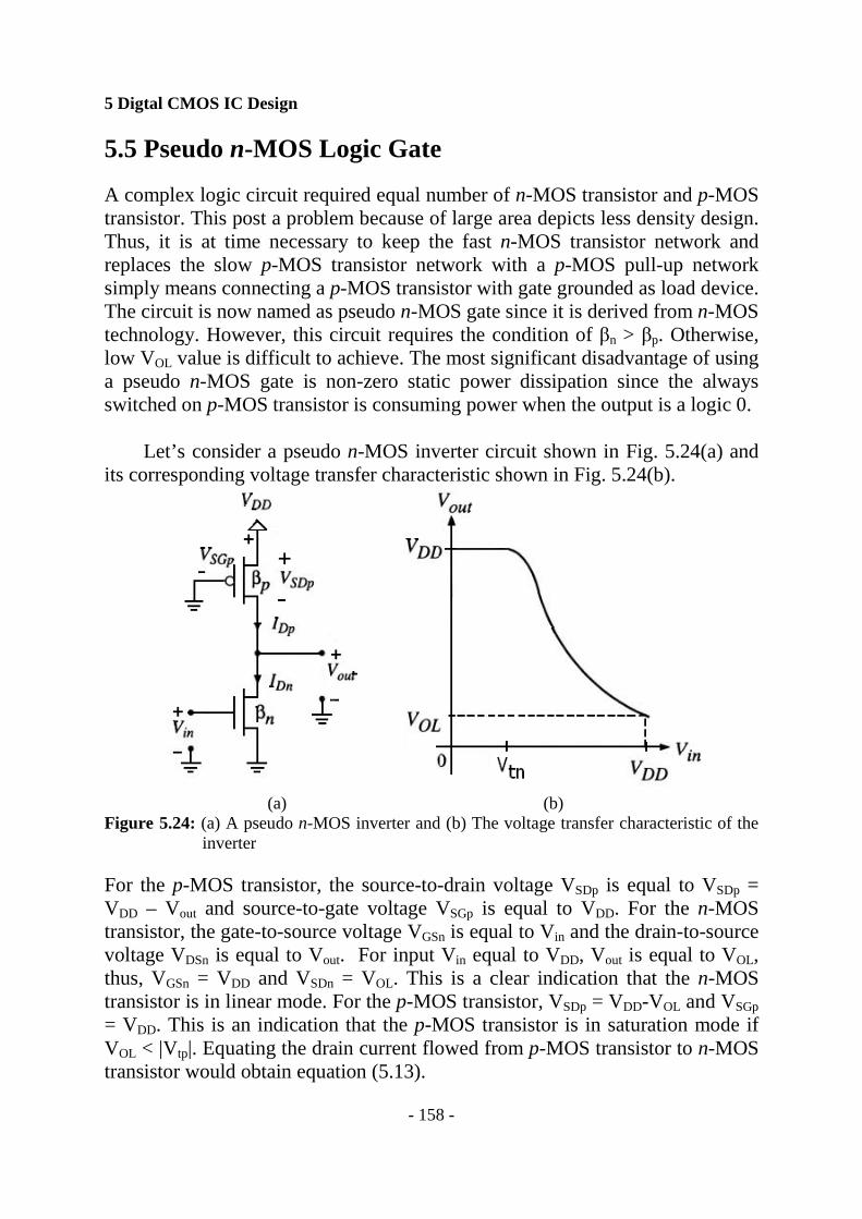
5.5 Pseudo n-MOS Logic Gate A complex logic circuit required equal number of n-MOS transistor and p-MOS transistor. This post a problem because of large area depicts less density design. Thus, it is at time necessary to keep the fast n-MOS transistor network and replaces the slow p-MOS transistor network with a p-MOS pull-up network simply means connecting a p-MOS transistor with gate grounded as load device. The circuit is now named as pseudo n-MOS gate since it is derived from n-MOS technology. However, this circuit requires the condition of βn > βp. Otherwise, low VOL value is difficult to achieve. The most significant disadvantage of using a pseudo n-MOS gate is non-zero static power dissipation since the always switched on p-MOS transistor is consuming power when the output is a logic 0.
Let’s consider a pseudo n-MOS inverter circuit shown in Fig. 5.24(a) and its corresponding voltage transfer characteristic shown in Fig. 5.24(b).
(a) (b)
Figure 5.24: (a) A pseudo n-MOS inverter and (b) The voltage transfer characteristic of the inverter
For the p-MOS transistor, the source-to-drain voltage VSDp is equal to VSDp = VDD – Vout and source-to-gate voltage VSGp is equal to VDD. For the n-MOS transistor, the gate-to-source voltage VGSn is equal to Vin and the drain-to-source voltage VDSn is equal to Vout. For input Vin equal to VDD, Vout is equal to VOL, thus, VGSn = VDD and VSDn = VOL. This is a clear indication that the n-MOS transistor is in linear mode. For the p-MOS transistor, VSDp = VDD-VOL and VSGp = VDD. This is an indication that the p-MOS transistor is in saturation mode if VOL < |Vtp|. Equating the drain current flowed from p-MOS transistor to n-MOS transistor would obtain equation (5.13).

5 Digtal CMOS IC Design
- 159 -
[ ] ( )2
tpDDP2
OLOLtnDDn VV
2VV)VV(2
2−
β=−−
β (5.13)
This equation gives rise to 2tpDD
n
P2tnDDtnDDOL )VV()VV()VV(V −
ββ
−−−−= ,
which indicates that for low VOL, condition βn > βp is required. The sheet resistance of the p-MOS transistor is about 2.5 times higher than the sheet resistance of the n-MOS transistor. As the rule of thumb, the resistance value of p-MOS transistor should be 5 times the resistance value of n-MOS transistor. This shall mean (L/W)p = 2(L/W)n. This implies that (W/L)n = 2(W/L)p.
The layout of a complex logic circuit function C)BA( +• design with pseudo n-MOS gate is shown in Fig. 5.25. Notice that the dimension of the n-MOS transistor network is two times larger than the grounded p-MOS transistor.
Figure 5.25: Layout of a complex logic function C)BA( +• designed with pseudo n-MOS
gate design concept One of the popular applications of pseudo n-MOS logic gate is the implementation of programmable logic array PLA. This device is originally

5 Digtal CMOS IC Design
- 160 -
created for standalone device that allows user to program for different functionality. The capability of PLA is limited and has been replaced by significantly more powerful field programmable gate arrays FPGA. Designer usually likes to develop PLA into a highly regular, multiple output structure for the ease of automatic layout generation. Indeed ROM is also designed using this concept.
The block of a PLA is shown in Fig. 5.26. It consists of an input buffer that
provides both non-inverting and inverting input and a two-level combinational circuits that provide sum-of-product SOP logic functions. The “AND” block is responsible for generate product term and the “OR” is responsible for selection of product term to form the desire logic output.
Figure 5.26: The block diagram of a PLA
The design examples of logic circuit using PLA is shown in Fig. 5.27.

5 Digtal CMOS IC Design
- 161 -
Figure 5.27: The design of logic circuit using PLA The circuit consists of a 2-input AND gate, a 2-input NOR gate, and an exclusive OR gate. The input buffer provides the inverting and non-inverting logic, which are A, B, A , and B . The row provides the product term. Row 1 shows the pseudo n-MOS BA + gate, which is also the product term BA ⋅ . Row 2 shows the pseudo n-MOS BA + gate, which is also the product term BA ⋅ . Row 3 shows the pseudo n-MOS BA + gate, which is also the product term
BA ⋅ . Row 4 shows the pseudo n-MOS BA + gate. Column 1 has a pseudo n-MOS inverter, whereby its input is connected to BA + , which will yield (A+B). However, after connected to an inverter, it yield back BA + logic. Column 2 has the input of the pseudo n-MOS inverter connected to )BA( ⋅ , which will result
BA ⋅ . However, after the inverter, it yields )BA( ⋅ logic. Column 3 has a 2-input pseudo n-MOS NOR gate, whereby its inputs are respectively connected to BA ⋅ and BA ⋅ , which would result exclusive NOR gate. However, after the inverter, it yields back exclusive OR logic.

5 Digtal CMOS IC Design
- 162 -
5.6Transmission Gate A CMOS transmission gate TG is designed by connecting an n-MOS and a p- MOS transistor in parallel as shown in Fig. 5.28.
(a) Circuit schematic (b) Circuit symbol (c) Circuit symbol
Figure 5.28: CMOS transmission gate The transmission gate is controlled by the signal S. Logic 1 connected to signal pin S switches on the n-MOS transistor, whilst logic 0 means S switches the p-MOS transistor. The transmission gate acts as a good electrical switch connecting between X input and Y output. The transmission gate can transmit the entire logic 0 voltage, which is VSS voltage and logic 1, which is VDD voltage. P-MOS transistor is used to transmit logic 1 since it can pass strong logic 1, whilst n-MOS transistor is used to transmit logic 0 since it can pass strong logic 0. The transmission gate TG is classified as bi-directional type, whereby Fig. 5.28(b) shows the meaning. The back-to-back arrow indicating that the data can flow in either direction. The symbol in Fig. 5.28(c) is another representation of transmission gate showing data X is transfer to Y output.
5.6.1 Electrical Characteristics The electrical characteristics of transmission gate shall be discussed in this section. Let’s examine transmitting logic 1 and logic 0 voltages through a transmission gate that has a capacitive load as shown in the circuit of Fig. 5.29. The input voltage is assumed to be at VDD, whilst the output voltage is taken across the capacitor. It is assumed that both transistors are biased into conduction with VDD voltage applied to the gate of the n-MOS transistor, and 0V applied to the gate of the p-MOS transistor. Using KCL, the output node as
5 Digtal CMOS IC Design
- 163 -
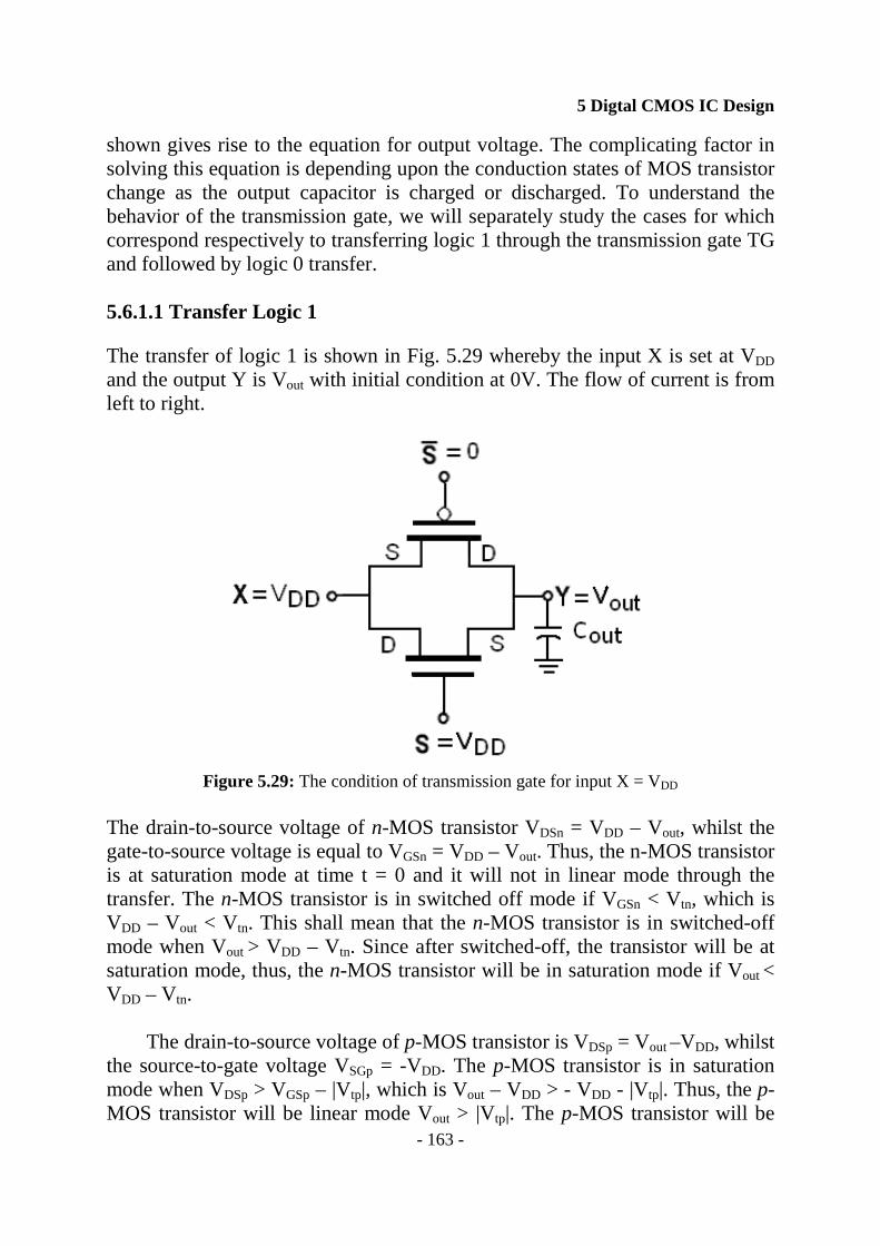
shown gives rise to the equation for output voltage. The complicating factor in solving this equation is depending upon the conduction states of MOS transistor change as the output capacitor is charged or discharged. To understand the behavior of the transmission gate, we will separately study the cases for which correspond respectively to transferring logic 1 through the transmission gate TG and followed by logic 0 transfer. 5.6.1.1 Transfer Logic 1 The transfer of logic 1 is shown in Fig. 5.29 whereby the input X is set at VDD and the output Y is Vout with initial condition at 0V. The flow of current is from left to right.
Figure 5.29: The condition of transmission gate for input X = VDD
The drain-to-source voltage of n-MOS transistor VDSn = VDD – Vout, whilst the gate-to-source voltage is equal to VGSn = VDD – Vout. Thus, the n-MOS transistor is at saturation mode at time t = 0 and it will not in linear mode through the transfer. The n-MOS transistor is in switched off mode if VGSn < Vtn, which is VDD – Vout < Vtn. This shall mean that the n-MOS transistor is in switched-off mode when Vout > VDD – Vtn. Since after switched-off, the transistor will be at saturation mode, thus, the n-MOS transistor will be in saturation mode if Vout < VDD – Vtn.
The drain-to-source voltage of p-MOS transistor is VDSp = Vout –VDD, whilst
the source-to-gate voltage VSGp = -VDD. The p-MOS transistor is in saturation mode when VDSp > VGSp – |Vtp|, which is Vout – VDD > - VDD - |Vtp|. Thus, the p-MOS transistor will be linear mode Vout > |Vtp|. The p-MOS transistor will be
5 Digtal CMOS IC Design
- 164 -
switched mode if VGSp < |Vtp|. This implies that |Vtp| > VDD, which cannot be happened. Therefore, the p-MOS transistor is never in switched-off mode.
Since Vout voltage is gradually increased from 0V to VDD, one can see that
the n-MOS transistor is changing from saturation mode to cut-off mode when Vout > VDD – Vtn. The p-MOS transistor changes from saturation mode to linear mode when Vout > |Vtp|.
The analysis also shows that there are three operating regions for the
transmission gate. The first region both n-MOS and p-MOS transistors are in saturation mode until the Vout is equal to |Vtp|. The second region is for Vout
ranges from Vtp to (VDD – Vtn). In this region, the n-MOS transistor is in saturation and p-MOS transistor is in linear region. The third region is for Vout ranges from (VDD – Vtn) to VDD. In this region, the n-MOS transistor is in cut-off mode and p-MOS transistor is in linear mode.
The channel resistance for various regions can be analyzed based on the
equation for channel resistance, which is Rp,n = n,p,D
n,p,DS
I
V. In third region, only p-
MOS transistor is in linear region, therefore, the channel resistance Rp is
Rp = [ ])VV()VV(2
2
outDDtpDD −−−β (5.14)
Student is encouraged to derive the channel resistance of the transmission gate for region I and II.
Figure 5.30 summaries the mode state of the n-MOS and p-MOS transistors during the output transition from 0V to VDD.

5 Digtal CMOS IC Design
- 165 -
Figure 5.30: The Mode condition of n-MOS and p-MOS transistors during output transition from logic 0 to logic 1
5.6.1.2 Transfer Logic 0 The transfer of logic 0 can be analyzed with the aid of Fig. 5.31, where the flow of current is from right to left side of the transmission gate. The drain-to-source voltage of the n-MOS transistor is VDSn = Vout, whilst the gate-to-source voltage is equal to VGSn = VDD. Thus, the n-MOS transistor is in saturation mode at time t = 0. This shall mean that the n-MOS transistor is in saturation mode if Vout > VDD – Vtn. The n-MOS transistor will be in linear mode if Vout < VDD – Vtn. The n-MOS transistor is in switched off mode if VGSn < Vtn, which is VDD < Vtn. This cannot be happened. Thus, the n-MOS transistor is never in switched-off mode during the logic 0 transfers.
The drain-to-source voltage of p-MOS transistor is VDSp = -Vout, whilst the gate-to-source voltage VGSp = -VDD. Thus, the p-MOS transistor is in saturation mode at time t = 0. The p-MOS transistor is in saturation mode when VDSp > VGSp – |Vtp|, which is - Vout > - VDD - |Vtp|. This implies that Vout < VDD +|Vtp|. If the p-MOS transistor is in linear mode, this means that Vout > VDD + |Vtp|, in which it cannot be happened. Thus, the p-MOS transistor is never in linear mode during the transfer of logic 0. The p-MOS transistor is in cut-off mode when VGSp < |Vtp|, which is Vout <|Vtp|.

5 Digtal CMOS IC Design
- 166 -
Figure 5.31: The condition of transmission gate for input X = 0 V
Since Vout voltage is gradually decreased from VDD to 0V, this draws the conclusion that there are three operating regions for the transmission gate. The first region both n-MOS and p-MOS transistors are in saturation mode until the Vout is equal to (VDD – Vtn). The second region is for Vout ranges from (VDD – Vtn) to Vtp. In this region, the p-MOS transistor is in saturation and n-MOS transistor is in linear region. The third region is for Vout ranges from Vtp to 0. In this region the p-MOS transistor is in cut-off mode and n-MOS transistor is in linear mode.
In third region, only n-MOS transistor is operating in linear region,
therefore, the channel resistance Rn is
Rn = [ ])V()VV(2
2
outtnDD −−β (5.15)
Figure 5.32 summaries that mode state of the n-MOS and p-MOS transistors during the output transition from VDD to 0V.

5 Digtal CMOS IC Design
- 167 -
Figure 5.32: The Mode condition of n-MOS and p-MOS transistors during output transition
from logic 1 to logic 0
5.6.2 RC Model of Transmission Gate The RC model of a transmission gate is shown in Fig.5.33. The capacitance of input side is denoted as CX and the output side is denoted as CY. RTG denotes resistance of the transmission gate. S denotes input to gate of n-channel MOS transistor of transmission gate, where the transistor is switched on. S input to n-channel MOS transistor means the transmission gate is switched off.
Figure 5.33: RC model of a transmission gate with input node X and output node Y
The input to the transmission is a step function Vin(t) = VDDu(t) for transfer from a logic 0 to logic 1. The output voltage Vout(t) is seen as the charging of capacitance Cout, which is comprised of CY and the load capacitance CLoad

5 Digtal CMOS IC Design
- 168 -
through resistance of transmission gate RTG. Thus, the Vout(t) is equal to Vout(t) = VDD[1-exp(-t/τTG)]. CY is equal to CGSn+Kn(0,VDD)CSBn+CGDp+ Kp(0,VDD)CDBp.
For a transfer of logic 1 to logic 0, the Vin(t) is Vin(t) = VDD[1–u(t)]. The output voltage Vout(t) is seeing discharging of through RTG and Cout. Thus, the output voltage Vout(t) is Vout(t) = VDDexp(-t/τTG). Note that u(t) = 0 for t = 0 and u(t) = 1 for t ≠ 0.
The resistance of the transmission gate RTG is generally calculated using
equation (5.16).
RTG = DnDp
TG
II
V
+ (5.16)
It is also equal to the parallel channel resistance of n-channel and p-channel MOS transistors. Depending on the condition of the logic transfer, the resistance of the transmission can be varied. Figure 5.34 shows the resistance of the transmission gate with various output voltage Vout condition for logic 1 transfer.
Figure 5.34: The RTG of a transmission gate with logic 1 transfer
Figure 5.35 shows the resistance of the transmission gate with various output voltage Vout condition for logic 0 transfer.

5 Digtal CMOS IC Design
- 169 -
Figure 5.35: The RTG of a transmission gate with logic 0 transfer
5.6.3 Application of Transmission Gate Let’s study the application of transmission gate in designing the logic circuits i.e. both the combinational and sequential circuits. Since transmission gate is made of a pair of n-MOS transistor and p-MOS transistor with complimentary gate control, thus a gate control A is split into A = )0A1A( ⋅+⋅ , where 1A ⋅ is used to control n-MOS transistor and 0A ⋅ is used to control p-MOS transistor.
The switching characteristic of transmission gate is particularly useful for designing multiplexer MUX circuit. The Boolean function of the 2-to-1 multiplexer is F = 1o PSPS ⋅+⋅ . Based on the function F, logic of Po is passed through the transmission gate when selected S is asserted low. Thus, when S is at logic 0 and S is at logic 1, the logic of P0 is passed. Likewise, when S is at logic 1 and S is at logic 0, the logic of P1 is passed. The function equation of the multiplexer can also be written as F = )0S1S(P)0S1S(P 10 ⋅+⋅+⋅+⋅ , where the term
in parenthesis corresponds to logic control of transmission gate. )0S1S(P0 ⋅+⋅
indicates that S is connected to n-MOS transistor and S is connected to p-MOS transfer, while P0 is connected in series with the transmission gate. )0S1S(P1 ⋅+⋅ indicates that S is connected to p-MOS transistor and S is connected to n-MOS

5 Digtal CMOS IC Design
- 170 -
transfer, while P1 is connected in series with the transmission gate. The logic circuit of 2-to-1 multiplexer is shown in Fig. 5.36.
Figure 5.36: A 2-to-1 multiplexer circuit
The Boolean function of exclusive-NOR gate is f(A, B) = BA ⊕ = BABA ⋅+⋅ . The function can also be written as f(A, B) = ( )0B1BA ⋅+⋅⋅ +A ( )0B1B ⋅+⋅ taking B as the control bit. This shall mean that input A is true only if p-MOS transistor controlled by bit B is true and A is true only if p-MOS transistor controlled by bit B is true. The detailed circuit is shown in Fig. 5.37.
Figure 5.37: CMOS circuit of a 2-input exclusive-NOR gate
The function of the exclusive OR gate can also be written as f(A, B) =
BA ⋅ + BA ⋅ = ( ) ( )0B1BA0B1BA ⋅+⋅⋅+⋅+⋅⋅ . The exclusive-OR gate design using transmission gate is shown in Fig. 5.38.

5 Digtal CMOS IC Design
- 171 -
Figure 5.38: CMOS circuit of an exclusive OR gate utilizing transmission gate The Boolean function of a two-input OR gate is f(A, B) = A + B = 0BA ⋅⋅ + 1BA ⋅⋅ + 1BA ⋅⋅ + 1BA ⋅⋅ = 0BA ⋅⋅ + A⋅1 + B⋅1 = B⋅ A +A⋅ A . Since the function f(A, B) of OR gate is A + B, this function can also be written as
=+⋅ ABA ( ) ( )0A1AA0A1AB ⋅+⋅⋅+⋅+⋅⋅ . The first term corresponds to a transmission gate with B as input and A as control.
The second term corresponds to either a p-MOS with A as input and A as
control or an n-MOS with A as input and A as control. Note that logic function 1AA ⋅⋅ always provides either open circuit or logic 1, which is an indication of
OR B circuit. The CMOS circuit of the two circuit of two-input OR gate designed using transmission gate and either p-MOS or n-MOS is shown in Fig. 5.39.

5 Digtal CMOS IC Design
- 172 -
Figure 5.39: CMOS OR gate designed with transmission gate
The Boolean function of a two-input AND gate is f(A, B) = A⋅B =
( ) ( )1B0BB0B1BA ⋅+⋅⋅+⋅+⋅⋅ . ( )0B1BA ⋅+⋅⋅ indicates that B is connected to the gate of n-MOS transistor of the transmission gate, while B is connected to the p-MOS transistor of the transmission gate. A is connected in series with the transmission gate. ( )1B0BB ⋅+⋅⋅ indicates that B is connected to the gate of p-MOS transistor of the transmission gate, while B is connected to the n-MOS transistor of the transmission gate. B is connected in series with the transmission gate. Since B is connected to transmission gate that is control by B or B . Therefore, one of the transistors of the second part of the transmission is sufficient to provide the necessary logic state. Moreover, BB ⋅ provides logic 0, when input B is at logic 0, otherwise the output will be undefined high impedance state. The logic circuit of the AND gate is shown in Fig. 5.40.
Figure 5.40: CMOS AND gate designed with transmission gate

5 Digtal CMOS IC Design
- 173 -
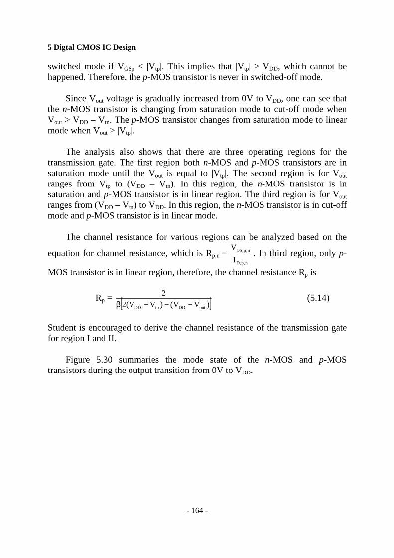
5.7 Domino Logic Circuit Domino CMOS logic circuit is an extension of dynamic logic circuit by adding in an inverter to prevent possibility of n-MOS-n-MOS transistor glitch. The general domino logic circuit is shown in Fig. 5.41.
When timing signal φ is at logic 0, the capacitor C is pre-charged to voltage VDD. The output shall be at logic 0. When timing signal φ is at logic 1, the domino circuit is in evaluation mode. Depending on the condition of the n-MOS transistor network, the charge in the capacitor may maintain to provide logic 0 at output or discharge through the n-MOS transistor network to provide logic 1 at output. Based on the circuit design, domino logic never provides inverting logic at the output.
Figure 5.41: General circuit of domino circuit design Domino circuit is always used in cascade design. The output of each stage is connected to a MOS transistor in next stage and the output of the later stage is then connected to a MOS transistor in the forward stage and so on. The example of the domino logic circuit of Boolean function of a three input OR gate is shown in Fig. 5.42.
5 Digtal CMOS IC Design
- 174 -
Figure 5.42: Domino circuit of a 3-input OR gate
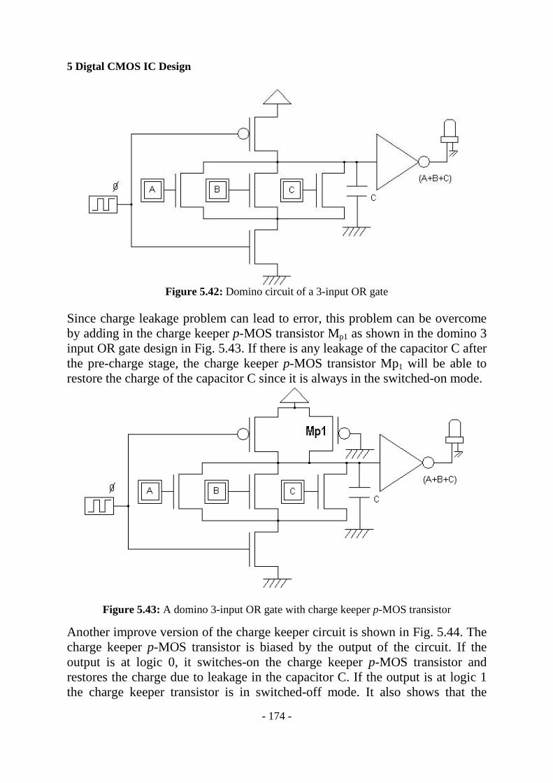
Since charge leakage problem can lead to error, this problem can be overcome by adding in the charge keeper p-MOS transistor Mp1 as shown in the domino 3 input OR gate design in Fig. 5.43. If there is any leakage of the capacitor C after the pre-charge stage, the charge keeper p-MOS transistor Mp1 will be able to restore the charge of the capacitor C since it is always in the switched-on mode.
Figure 5.43: A domino 3-input OR gate with charge keeper p-MOS transistor
Another improve version of the charge keeper circuit is shown in Fig. 5.44. The charge keeper p-MOS transistor is biased by the output of the circuit. If the output is at logic 0, it switches-on the charge keeper p-MOS transistor and restores the charge due to leakage in the capacitor C. If the output is at logic 1 the charge keeper transistor is in switched-off mode. It also shows that the

5 Digtal CMOS IC Design
- 175 -
evaluated result is logic 0, which shall mean that the capacitance should lose all the charges.
Figure 5.44: Domino circuit of a 3-input OR gate with feedback control to charge keeper p-MOS transistor
In order to prevent from the parasitic effect, an extra inverter Z can be added as feedback to the charge keeper p-MOS transistor Mp1. It also frees the output from slowdown due to induced flipping state of the feedback network. The 3 input OR gate domino circuit with the feedback inverter is shown in Fig. 5.45.
Figure 5.45: A domino 3-input OR gate with inverter feedback to charge keeper p-MOS
transistor
5 Digtal CMOS IC Design
- 176 -
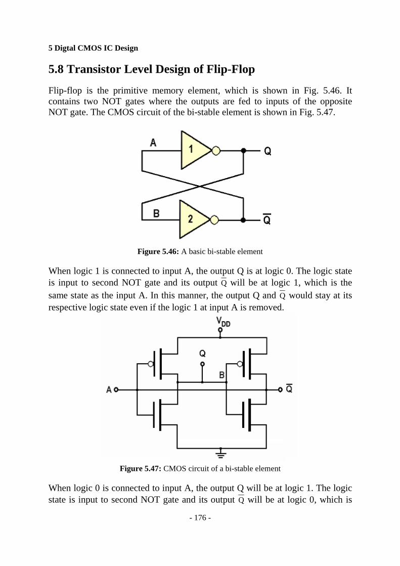
5.8 Transistor Level Design of Flip-Flop Flip-flop is the primitive memory element, which is shown in Fig. 5.46. It contains two NOT gates where the outputs are fed to inputs of the opposite NOT gate. The CMOS circuit of the bi-stable element is shown in Fig. 5.47.
Figure 5.46: A basic bi-stable element
When logic 1 is connected to input A, the output Q is at logic 0. The logic state is input to second NOT gate and its output Q will be at logic 1, which is the same state as the input A. In this manner, the output Q and Q would stay at its respective logic state even if the logic 1 at input A is removed.
Figure 5.47: CMOS circuit of a bi-stable element
When logic 0 is connected to input A, the output Q will be at logic 1. The logic state is input to second NOT gate and its output Q will be at logic 0, which is

5 Digtal CMOS IC Design
- 177 -
the same state as the input A. In this manner, the output Q and Q would remain at its respective logic state even if the logic 0 at input A is removed. Combining both conditions of logic states, the bi-stable element forms the basic memory bit. The layout of the bi-stable element is shown in Fig. 5.49.
Figure 5.49: The layout of the bi-stable element The bi-state element has two stable states and one unstable state. The unstable state occurs at the mid-point voltage. At this point all transistors are in saturation mode and also at the highest potential energy.
The SR flip-flop is shown in Fig. 5.50. The output Q is Q = QCLKS +⋅
and Q = QCLKR +⋅ . Using DeMorgan’s theorem, Q is also equal to Q = Q)CLKS( ⋅+ , which forms the p-MOS transistor circuit of the output Q. Output
Q is also equal to Q)CLKR( ⋅+ , which forms the p-MOS transistor circuit of output Q.

5 Digtal CMOS IC Design
- 178 -
Figure 5.50: SR flip-flop
Based on p-MOS and n-MOS transistors’ equations of the SR flip-flop, the CMOS circuit design of the SR flip-flop is shown in Fig. 5.51.
Figure 5.51: CMOS circuit of a SR flip-flop
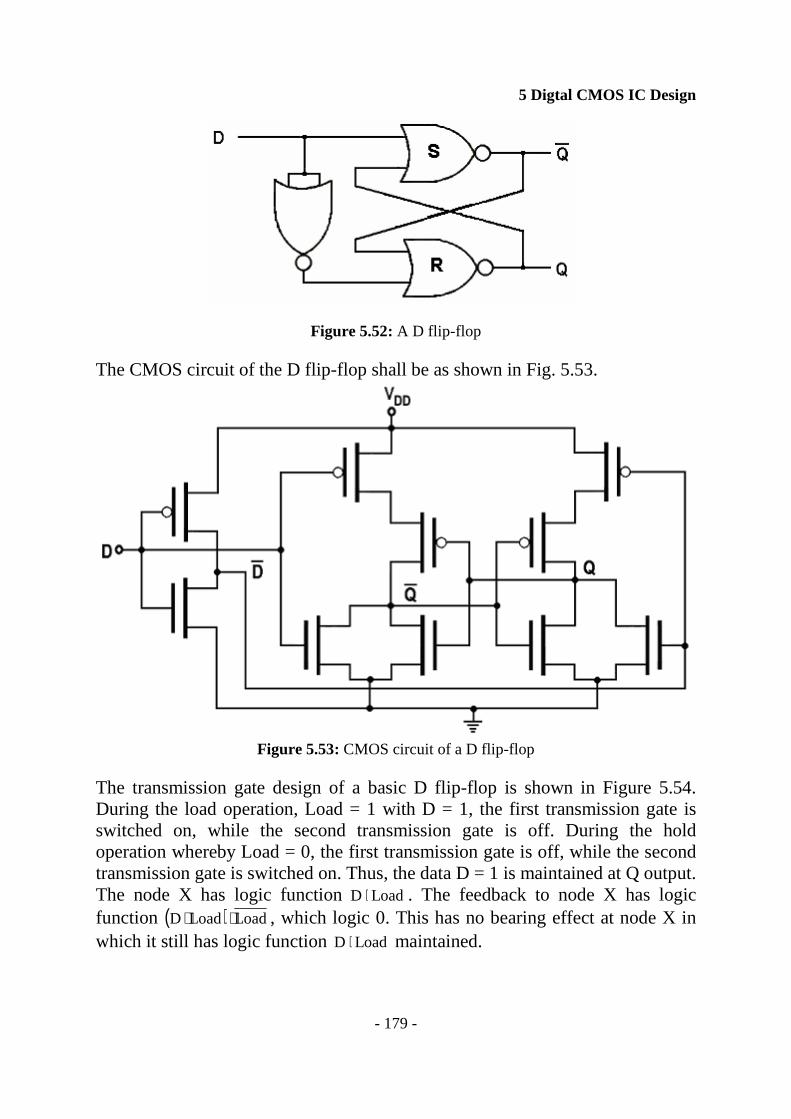
The D flip-flop is shown in Fig. 5.52. The output Q is Q = QD + = QD ⋅ , whilst
the output Q is Q = DQ + = DQ ⋅ .
5 Digtal CMOS IC Design
- 179 -
Figure 5.52: A D flip-flop The CMOS circuit of the D flip-flop shall be as shown in Fig. 5.53.
Figure 5.53: CMOS circuit of a D flip-flop
The transmission gate design of a basic D flip-flop is shown in Figure 5.54. During the load operation, Load = 1 with D = 1, the first transmission gate is switched on, while the second transmission gate is off. During the hold operation whereby Load = 0, the first transmission gate is off, while the second transmission gate is switched on. Thus, the data D = 1 is maintained at Q output. The node X has logic function LoadD ⋅ . The feedback to node X has logic function ( ) LoadLoadD ⋅⋅ , which logic 0. This has no bearing effect at node X in which it still has logic function LoadD ⋅ maintained.

5 Digtal CMOS IC Design
- 180 -
Figure 5.54: Transmission gate design of a D flip-flop
Another compact way to design a D flip-flop is shown in Fig. 5.55. The output at node X is LoadD ⋅ + LoadD ⋅ , which is equal to D. Thus, data D is latched when Load is equal to logic 1.
Figure 5.55: Compact design of D flip-flop
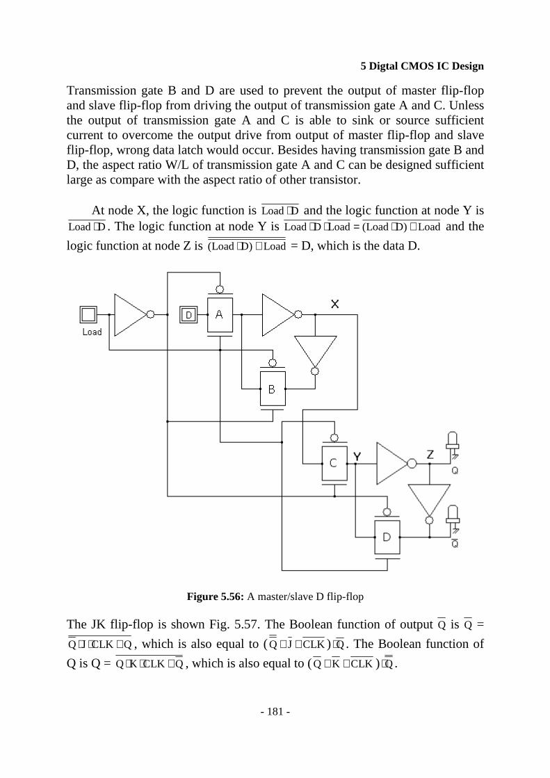
In order to avoid wrong data being latch into the D flip-flop, the D flip-flop can be designed with master/slave operation that utilizing transmission gate and NOT gates. Figure 5.56 shows the CMOS design of a master/slave D flip-flop.
5 Digtal CMOS IC Design
- 181 -
Transmission gate B and D are used to prevent the output of master flip-flop and slave flip-flop from driving the output of transmission gate A and C. Unless the output of transmission gate A and C is able to sink or source sufficient current to overcome the output drive from output of master flip-flop and slave flip-flop, wrong data latch would occur. Besides having transmission gate B and D, the aspect ratio W/L of transmission gate A and C can be designed sufficient large as compare with the aspect ratio of other transistor.
At node X, the logic function is DLoad⋅ and the logic function at node Y is DLoad⋅ . The logic function at node Y is Load)DLoad(LoadDLoad +⋅=⋅⋅ and the
logic function at node Z is Load)DLoad( +⋅ = D, which is the data D.
Figure 5.56: A master/slave D flip-flop
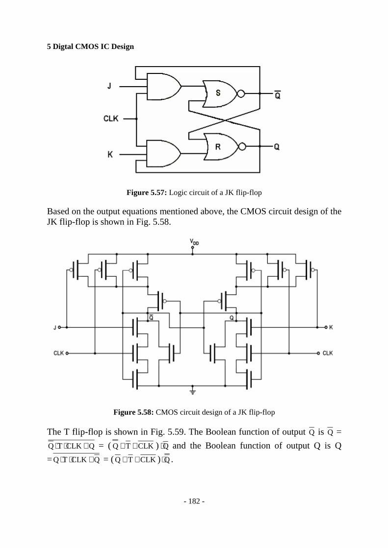
The JK flip-flop is shown Fig. 5.57. The Boolean function of output Q is Q =
QCLKJQ +⋅⋅ , which is also equal to ( CLKJQ ++ ) Q⋅ . The Boolean function of
Q is Q = QCLKKQ +⋅⋅ , which is also equal to ( CLKKQ ++ ) Q⋅ .
5 Digtal CMOS IC Design
- 182 -
Figure 5.57: Logic circuit of a JK flip-flop Based on the output equations mentioned above, the CMOS circuit design of the JK flip-flop is shown in Fig. 5.58.
Figure 5.58: CMOS circuit design of a JK flip-flop
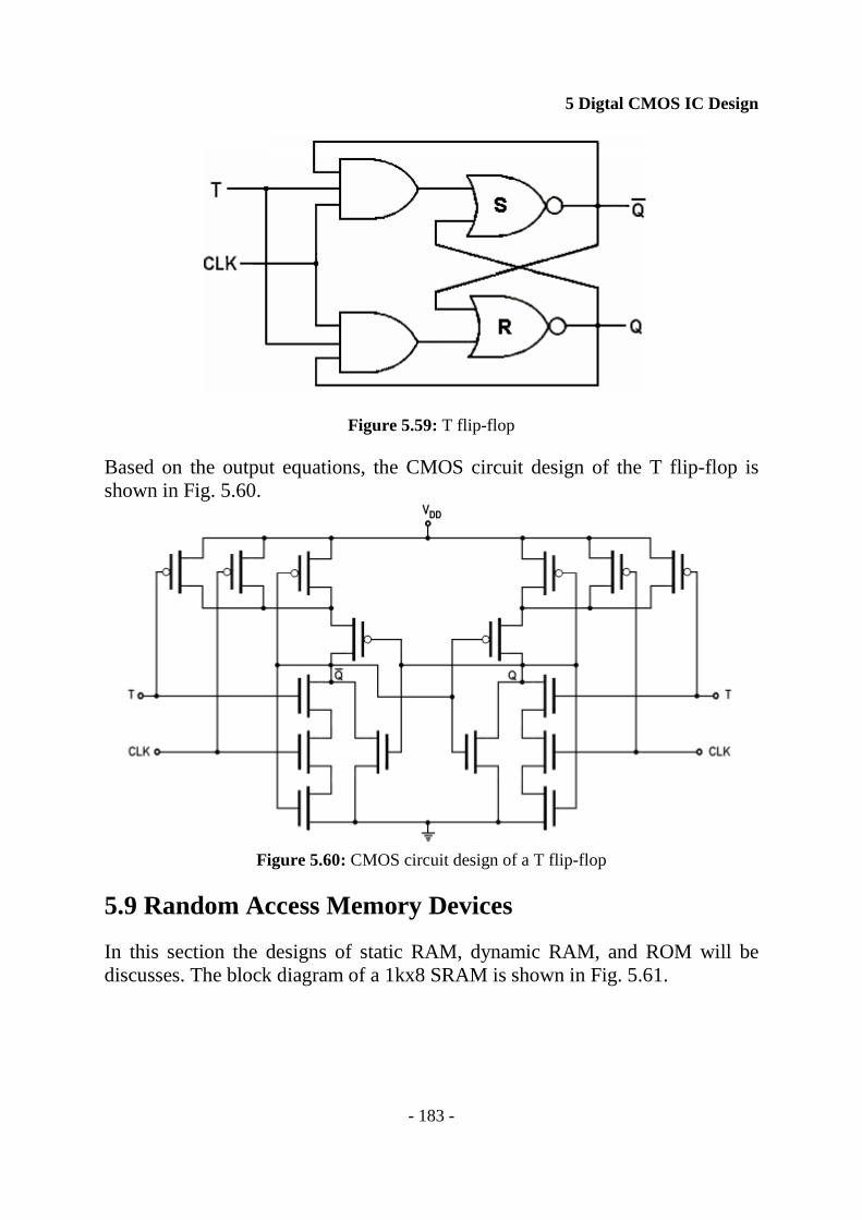
The T flip-flop is shown in Fig. 5.59. The Boolean function of output Q is Q =
QCLKTQ +⋅⋅ = ( CLKTQ ++ ) Q⋅ and the Boolean function of output Q is Q
= QCLKTQ +⋅⋅ = ( CLKTQ ++ ) Q⋅ .
5 Digtal CMOS IC Design
- 183 -
Figure 5.59: T flip-flop Based on the output equations, the CMOS circuit design of the T flip-flop is shown in Fig. 5.60.
Figure 5.60: CMOS circuit design of a T flip-flop
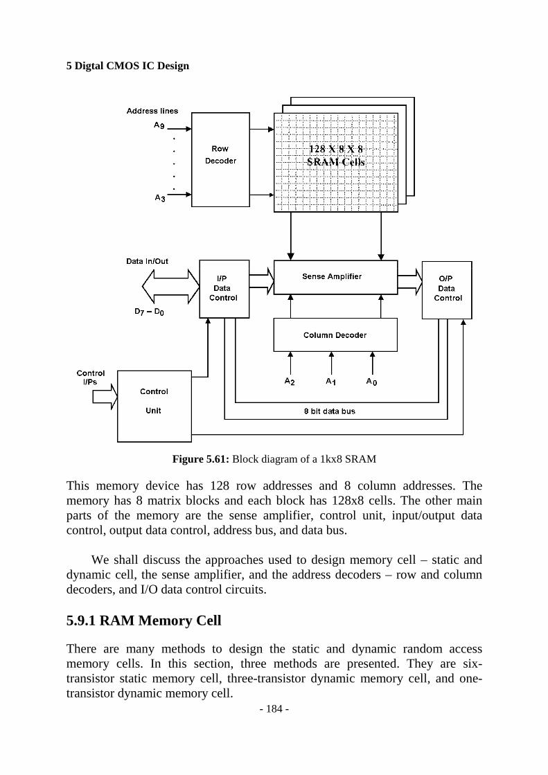
5.9 Random Access Memory Devices In this section the designs of static RAM, dynamic RAM, and ROM will be discusses. The block diagram of a 1kx8 SRAM is shown in Fig. 5.61.
5 Digtal CMOS IC Design
- 184 -
Figure 5.61: Block diagram of a 1kx8 SRAM
This memory device has 128 row addresses and 8 column addresses. The memory has 8 matrix blocks and each block has 128x8 cells. The other main parts of the memory are the sense amplifier, control unit, input/output data control, output data control, address bus, and data bus.
We shall discuss the approaches used to design memory cell – static and dynamic cell, the sense amplifier, and the address decoders – row and column decoders, and I/O data control circuits. 5.9.1 RAM Memory Cell There are many methods to design the static and dynamic random access memory cells. In this section, three methods are presented. They are six-transistor static memory cell, three-transistor dynamic memory cell, and one-transistor dynamic memory cell.
5 Digtal CMOS IC Design
- 185 -
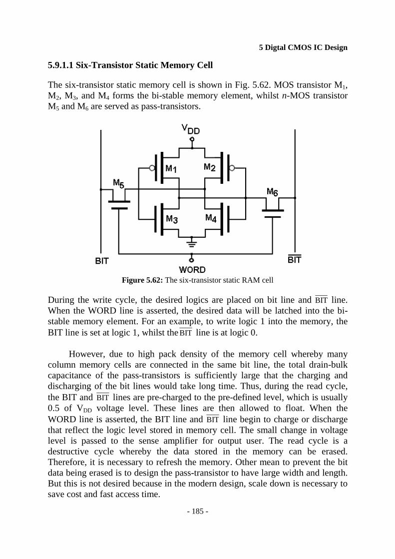
5.9.1.1 Six-Transistor Static Memory Cell The six-transistor static memory cell is shown in Fig. 5.62. MOS transistor M1, M2, M3, and M4 forms the bi-stable memory element, whilst n-MOS transistor M5 and M6 are served as pass-transistors.
Figure 5.62: The six-transistor static RAM cell
During the write cycle, the desired logics are placed on bit line and BIT line. When the WORD line is asserted, the desired data will be latched into the bi-stable memory element. For an example, to write logic 1 into the memory, the BIT line is set at logic 1, whilst theBIT line is at logic 0.
However, due to high pack density of the memory cell whereby many column memory cells are connected in the same bit line, the total drain-bulk capacitance of the pass-transistors is sufficiently large that the charging and discharging of the bit lines would take long time. Thus, during the read cycle, the BIT and BIT lines are pre-charged to the pre-defined level, which is usually 0.5 of VDD voltage level. These lines are then allowed to float. When the WORD line is asserted, the BIT line and BIT line begin to charge or discharge that reflect the logic level stored in memory cell. The small change in voltage level is passed to the sense amplifier for output user. The read cycle is a destructive cycle whereby the data stored in the memory can be erased. Therefore, it is necessary to refresh the memory. Other mean to prevent the bit data being erased is to design the pass-transistor to have large width and length. But this is not desired because in the modern design, scale down is necessary to save cost and fast access time.

5 Digtal CMOS IC Design
- 186 -
5.9.1.2 Three-Transistor Dynamic Memory Cell The three-transistor dynamic RAM structure is shown in Fig. 5.63. Transistor M1 is used to write the BIT logic into the source of transistor M1 and gate of transistor M2. With the present of source capacitance CS, depending on the logic being written, the gate voltage of transistor M2 is either at logic 0 or logic 1 that has voltage (VDD – Vtn(M2)) due to threshold loss.
Figure 5.63: A three-transistor dynamic RAM cell The BIT value is logic 0 then the gate voltage shall be 0V. If the BIT value is at logic 1 then the gate voltage will be at logic 1 that has voltage (VWrite – Vtn(M2)). This voltage is held on as long as the Read transistor M3 is not switched on.
During the read cycle, transistor M3 is switched on and if the BIT value is logic 1 then the BIT line would turn logic 0. Likewise, if the BIT value is logic 0 then upon reading the BIT line would turn to logic 1 that has maximum value (VRead – Vtn(M3)).
5 Digtal CMOS IC Design
- 187 -
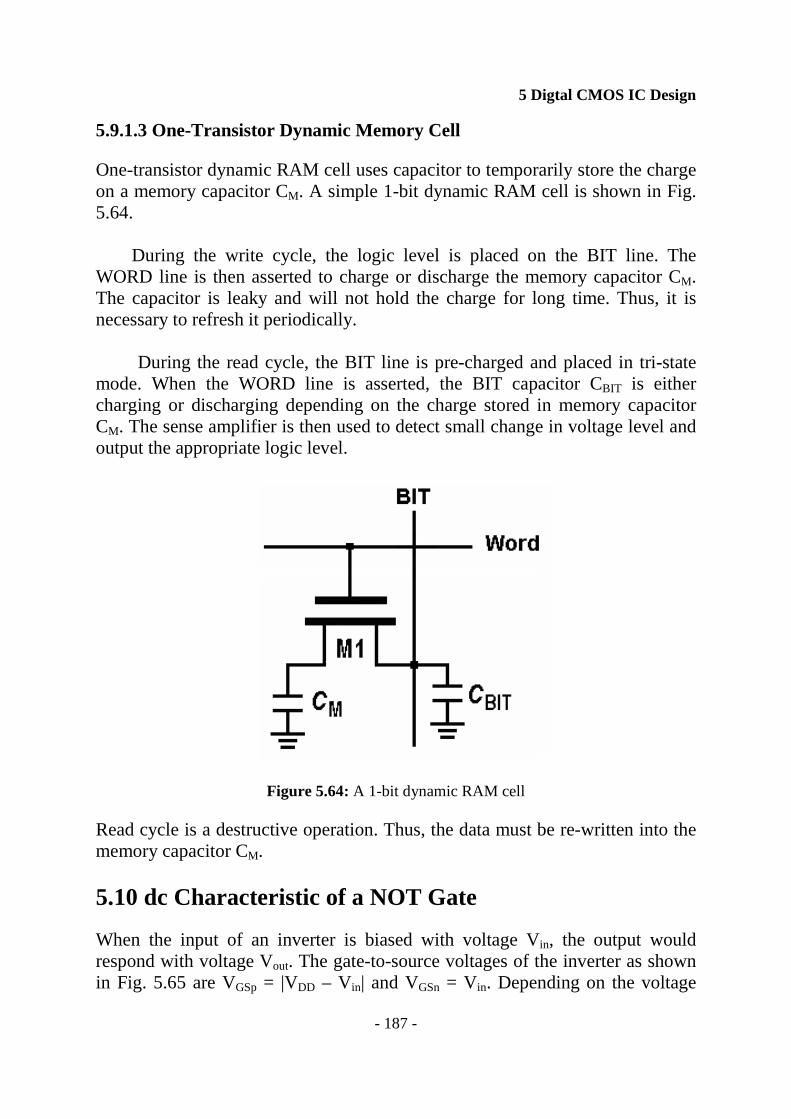
5.9.1.3 One-Transistor Dynamic Memory Cell One-transistor dynamic RAM cell uses capacitor to temporarily store the charge on a memory capacitor CM. A simple 1-bit dynamic RAM cell is shown in Fig. 5.64.
During the write cycle, the logic level is placed on the BIT line. The
WORD line is then asserted to charge or discharge the memory capacitor CM. The capacitor is leaky and will not hold the charge for long time. Thus, it is necessary to refresh it periodically.
During the read cycle, the BIT line is pre-charged and placed in tri-state
mode. When the WORD line is asserted, the BIT capacitor CBIT is either charging or discharging depending on the charge stored in memory capacitor CM. The sense amplifier is then used to detect small change in voltage level and output the appropriate logic level.
Figure 5.64: A 1-bit dynamic RAM cell Read cycle is a destructive operation. Thus, the data must be re-written into the memory capacitor CM.
5.10 dc Characteristic of a NOT Gate When the input of an inverter is biased with voltage Vin, the output would respond with voltage Vout. The gate-to-source voltages of the inverter as shown in Fig. 5.65 are VGSp = |VDD – Vin| and VGSn = Vin. Depending on the voltage

5 Digtal CMOS IC Design
- 188 -
value of Vin which can be ranged from 0 to VDD volt, the minimum and maximum values of the VGSp are 0 and VDD respectively. Similarly, VGSn also has the same minimum and maximum values.
When the value of either VGSn or |VGSp| is increased from 0V to VDD volt, the state of n-MOS transistor and p-MOS transistor moved from cut-off to saturation region and then move into linear region. This is clearly demonstrated when the value of VGSn or VGSp are less than the value of Vtn or |Vtp|, the transistors are in cut-off state. When the values of VGSn or VGSp are greater than the value of Vtn or |Vtp|, the transistors move into saturation region. This is because VDS of transistor is greater the value of (VGSn – vtn) or (VGSp - |Vtp|). The transistors finally move to linear state when the values of (VGSn – vtn) or (VGSp - |Vtp|) are greater than VDS.
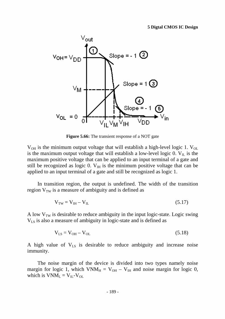
The voltage transfer characteristic VTC of a NOT gate or inverter is shown
in Fig. 5.66. It is a plot of output voltage Vout versus input voltage Vin. When the input voltage is VDD, the output voltage Vout will swing to 0V, which is VOL = 0V. When input voltage Vin is set at 0V, the output will swing to VDD, which is VOH and it is equal to VDD.
Figure 5.65: The voltage bias condition of an inverter or NOT gate The voltage transfer characteristic VTC of an inverter has three distinct regions; the low input region where Vin < VIL, the transition region where VIL ≤ Vin ≤ VIH, and the high input region Vin > VIH. The output has two transitions, one at V in = VIL and one at Vin = VIH. The transition is defined as the region between point 2 and 4 where the slope = -1.
5 Digtal CMOS IC Design
- 189 -
Figure 5.66: The transient response of a NOT gate
VOH is the minimum output voltage that will establish a high-level logic 1. VOL is the maximum output voltage that will establish a low-level logic 0. VIL is the maximum positive voltage that can be applied to an input terminal of a gate and still be recognized as logic 0. VIH is the minimum positive voltage that can be applied to an input terminal of a gate and still be recognized as logic 1.
In transition region, the output is undefined. The width of the transition region VTW is a measure of ambiguity and is defined as VTW = VIH – VIL (5.17) A low VTW is desirable to reduce ambiguity in the input logic-state. Logic swing VLS is also a measure of ambiguity in logic-state and is defined as VLS = VOH – VOL (5.18) A high value of VLS is desirable to reduce ambiguity and increase noise immunity.
The noise margin of the device is divided into two types namely noise margin for logic 1, which VNMH = VOH – VIH and noise margin for logic 0, which is VNML = VIL-VOL
5 Digtal CMOS IC Design
- 190 -
At point 1, the p-MOS transistor is in ohmic region and n-MOS transistor is at cut-off region. This region corresponds to output at logic 1.
At point 2, it is the region where the gradient of the VTC is -1. This is the
point that the input low voltage VIL and output high voltage VOH can be determined. Based on the condition at this point, saturation current of n-MOS transistor is equal to linear current of p-MOS transistor. Thus,
( ) [ ]2outDDoutDDtpinDD
P2tnin
n )VV()VV|)(V|VV(22
VV2
−−−−−β
=−β
(5.19)
To derive 1dV
dV
in
out −= , one needs to perform partial differentiation at both sides of
equation (5.19), which is dependent on Vin at left-hand side and dependent on V in and Vout at right-hand side. Thus,
outout
Dpin
in
Dpin
in
Dn dVV
IdV
V
IdV
dV
dI ⋅∂∂
+⋅∂∂
=⋅ (5.20)
Rearranging equation (5.20), it yields equation (5.21).
1
V
IV
I
dV
dI
dV
dV
out
Dp
in
Dp
in
Dn
in
out −=
∂∂
∂∂
−= (5.21)
Substituting the derivative, it yields equation (5.22), which is
tnp
ntpDDout
p
nin V|V|VV21V
ββ
+−−=
ββ
+ (5.22)
One may take equation (5.19) and (5.22) to solve for two unknowns, which are V in = VIL and Vout = VOH respectively.
Point 3 is the mid-point voltage point, where the input voltage Vin is equal to output voltage Vout. At mid-point voltage VM or switching voltage, both n-MOS and p-MOS transistors are in saturation mode. The mid-point voltage VM can be derived by equating the saturation current of the p-MOS and the n-MOS

5 Digtal CMOS IC Design
- 191 -
transistors, and setting output voltage Vout = VM, which is ( )2tnM
n VV2
−β =
( )2tpMDD
p |V|VV2
−−β
. This yields equation (5.23).
VM =
p
n
tnp
ntpDD
1
V|V|V
ββ
+
ββ+−
(5.23)
From equation (5.23), it shows that the mid-point voltage VM is determined by
the ratio of p
n
ββ . In order to get symmetrical inverter VTC, the mid-point
voltage VM should be equal to VDD/2. This corresponds to p
n
ββ = 1. This shall
mean that βn of n-MOS transistor should be same as βp of p-MOS transistor. Knowing that the mobility of n-MOS transistor is 2 to 3 times higher than the mobility of p-MOS transistor, therefore, the aspect ratio of p-MOS transistor should be 2 to 3 times larger than the aspect ratio of n-MOS transistor for obtaining symmetrical inverter VTC.
Based on equation (5.23), increasingp
n
ββ value gives lower mid-point
voltage VM.
At point 4, the p-MOS transistor is in saturation region and n-MOS transistor is in linear region. This point corresponds to the end of transition and output begins to go to logic 0. This is the region where the gradient of the VTC is also equal to -1, where the input high voltage VIH and actual output low voltage VOL can be determined. Based on the condition at this point saturation p-MOS transistor current is equal to linear n-MOS transistor current. Thus,
( ) [ ]2outouttnin
n2tpinDD
p VV)VV(22
|V|VV2
−−β
=−−β
(5.24)
To derive 1dV
dV
in
out −= , one needs to partial differentiation both sides of equation
(5.19), which dependent on voltage Vin at left-hand side and dependent on Vin and Vout at right-hand side. Thus,
5 Digtal CMOS IC Design
- 192 -
outout
Dnin
in
Dnin
in
Dp dVV
IdV
V
IdV
dV
dI⋅
∂∂
+⋅∂∂
=⋅ (5.25)
Rearranging equation (5.25), it yields equation (5.26).
1
V
IV
I
dV
dI
dV
dV
out
Dn
in
Dn
in
Dp
in
out −=
∂∂
∂∂
−= (5.26)
Substituting the derivative into equation (5.26), it yields equation (5.27).
( )|V|VVV21V tpDDn
ptnout
n
pin −
ββ
++=
ββ
+ (5.27)
One may take equation (5.24) and (5.27) to solve for two unknowns, which are V in = VIH and Vout = VOL respectively.
In region 5, the p-MOS transistor is in cut-off region, whilst the n-MOS transistor is in ohmic region. This is the region where the output is at logic 0.
5.11 ac Characteristics of a NOT Gate The ac characteristic of a NOT gate, which is its switching waveform, is shown in Fig. 5.67. tf is the fall time and tr is the rise time. The output does not respond immediately upon changing the input voltage because there is capacitance and resistance associated with the inverter whereby the charging and discharging of the capacitance cause the delay of response at the output.

5 Digtal CMOS IC Design
- 193 -
Figure 5.67: Switching of the NOT gate
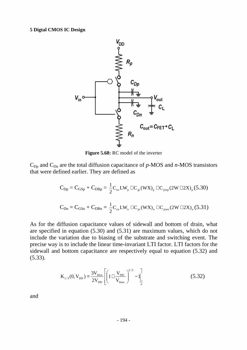
The RC model of the NOT gate is shown in Fig. 5.68. Rp and Rn are the channel resistances of the p-MOS and n-MOS transistors, which can be calculated from the ohmic equation of the MOS transistor by assuming the largest possible gate-to-source voltage VGS be equal to VDD. Thus, the channel resistance is Rn =
)VV( tnDDn −βη , where η ranges from 1 to 6 depending on technology. For
simplicity η is equal to 1. Applying η = 1 to the channel resistance of the n-MOS and p-MOS transistors respectively, they become
Rn = )VV(
1
tnDDn −β (5.28)
Rp = |)V|V(
1
tpDDp −β (5.29)
Rsn and Rsp are sheet resistances of n-MOS and p-MOS transistor respectively. For 0.12µm and VDD = 1.2V technology, the sheet resistances are respectively equal to Rsn = 1.8kΩ/ and Rsp = 5.5 kΩ/ respectively.
5 Digtal CMOS IC Design
- 194 -
Figure 5.68: RC model of the inverter
CDp and CDn are the total diffusion capacitance of p-MOS and n-MOS transistors that were defined earlier. They are defined as
CDp = CGSp + CDBp = pjswppjppox )X2W2(C)WX(CLWC2
1 +++ (5.30)
CDn = CGSn + CDBn = njswnnjnnox )X2W2(C)WX(CLWC2
1 +++ (5.31)
As for the diffusion capacitance values of sidewall and bottom of drain, what are specified in equation (5.30) and (5.31) are maximum values, which do not include the variation due to biasing of the substrate and switching event. The precise way is to include the linear time-invariant LTI factor. LTI factors for the sidewall and bottom capacitance are respectively equal to equation (5.32) and (5.33).
−
+= 1
V
V1
V2
V3)V,0(K
3/2
bisw
DD
DD
biswDD3/1 (5.32)
and
5 Digtal CMOS IC Design
- 195 -
−
+= 1
V
V1
V
V2)V,0(K
2/1
bibott
DD
DD
bisbottDD2/1 (5.33)
The sum of drain capacitance of n-MOS and p-MOS transistors is termed as capacitance of NOT gate CFET or it can be called as internal capacitance of the NOT gate. Thus,
CFET = Cint = CDn + CDp (5.34)
The load capacitance CL is depending on the number of gate driven by the inverter and the line capacitance Cmetal of the metal interconnect, which is defined in equation (10.4). Therefore, the load capacitance CL is equal to CL = FO(CGn + CGP) + Cmetal (5.35) where FO is the fan-out value.
The total output capacitance Cout of the NOT gate is now equal to the sum of capacitance CFET and the load capacitance CL, which is Cout = CFET + CL (5.36) If the inverter drives three NOT gates then the load capacitance CL is equal to 3(CGn + CGp) plus metal interconnect capacitance Cmetal, where CGn and CGp are the gate capacitance of the n-MOS and p-MOS transistors of the circuit driven by the inverter. Note that in this case, the Fan-out value FO is equal to three. 5.11.1 Fall Time of NOT Gate The discharge time of the NOT gate is defined as the time taken for the output of the NOT gate to fall from logic 1 to logic 0 through resistance Rn. Initially the output voltage is at VDD and is discharged to zero volt though the switched-on resistance of the n-MOS transistor. It follows the normal capacitor discharge equation, which is Vout = VDD exp(-t/τn) (5.37) where τn is the time constant, which is equal to CoutRn. Rewriting equation (5.37) as time t, it yields equation (5.38).

5 Digtal CMOS IC Design
- 196 -
t = τnout
DD
V
Vln (5.38)
The fall time tf is defined as the time taken for the output to fall from 90% of its maximum output value to 10% of its maximum output value. Thus, fall time tf is equal to
tf = τnDD
DD
V1.0
Vln -τn
DD
DD
V9.0
Vln = τn )9ln( = 2.2τn (5.39)
The fall time is tf = 2.2τn = 2.2(RnCout) = )VV(
C2.2
tnDDn
out
−β. Since VDD >> Vtn,
therefore, the fall time tf can be estimated as tf = DDn
out
V
C2.2
β. The fall time tf is also
known as tHL transition time.
5.11.2 Rise Time of NOT gate The charging time of the NOT gate is time taken for the output of the NOT gate to rise from logic 0 to logic 1 voltage through resistance Rp. Initially, the output voltage is at zero volt and is charged to VDD volt through the switched-on resistance of the p-MOS transistor, which follows the normal capacitor charging equation, which is Vout = VDD [1-exp(-t/τp)] (5.40) where τp is the time constant equals to CoutRp. Rewriting equation (5.40) as time t, it yields equation (5.41).
tr = τpoutDD
DD
VV
Vln
− (5.41)
The rise time tr is defined as the time taken for the output to rise from 10% of its maximum output value to 90% of its maximum output value. Thus, rise time tr is equal to
tr= τpDDDD
DD
V9.0V
Vln
−- τp
DDDD
DD
V1.0V
Vln
−= τp )9ln( = 2.2τp (5.42)
5 Digtal CMOS IC Design
- 197 -
The rise time is tr = 2.2τp = 2.2(RpCout) = |)V|V(
C2.2
tpDDp
out
−β. Since VDD >> |Vtp|,
therefore, the rise time tr can be estimated to be equal to tr = DDp
out
V
C2.2
β.
The fall time tf is known as tHL time, the high-to-low transition time since
it is the time taken to transit from logic 1 to logic 0. Similarly, the rise time tr is also known as tLH, the low-to-high transition time since it is the time taken for the output to transit from logic 0 to logic 1.
The reciprocal of the sum of fall time tf and rise time tr is a time value
used to determine the maximum operating frequency fmax of the NOT gate, which is shown in equation (5.43).
fmax = rf tt
1
+ (5.43)
Knowing that time constant τn = RnCout, τp = RpCout and total capacitance Cout = CFET + CL, the fall time tf and rise time tr are arranged respectively equal to tf = 2.2τn = 2.2 Rn(CFET + CL) = tf0 + αpCL (5.44) tr= 2.2τp = 2.2 Rp(CFET + CL) = tr0 + αnCL (5.45) where tf0 = 2.2RnCFET and tr0 = 2.2RpCFET are design dependent values. αp and αn are respectively equal to αp = 2.2Rp and αn = 2.2Rn. From equation (5.44) and (5.45), one can see that the fall time tf and rise time tr of the NOT gate are dependent on the external load capacitance CL. 5.11.3 Propagation Delay Time of NOT Gate Propagation delay time tp is often used to estimate the “reaction” delay time from input to output. When step-like input voltage is used, propagation delay time tp is defined as
tp = 2
tt pn rf + (5.46)
where tnf is the time taken for the output to fall from its maximum output voltage to 50% of its maximum output voltage. Thus, from equation (5.38), tnf is

5 Digtal CMOS IC Design
- 198 -
equal to τnln(2). Tpr is the time taken for the output to rise from zero volt to 50% of its maximum output voltage. From equation (5.41), tpr is equal to τpln(2). Based on the above analysis, the propagation delay time tp is equal to
tp = 2
2ln (τn + τp) (5.47)
Knowing that τn = RnCout, τp = RpCout and Cout = CFET + CL, equation (5.47) shall be
tp = 2
2ln (CFET + CL)(Rn + Rp) (5.48)
From equation (5.48), one can see that the propagation delay time tp of the NOT is dependent on the load capacitance CL, which has the same conclusion as shown by equation (5.44) and (5.45) for fall time and rise time.
5.12 Electrical Analysis of NAND Gate The transistor level circuit of a NAND gate is shown in Fig. 5.69. Since the device has two inputs, it implies that the NAND has more than one voltage transfer characteristic curve VTC. As the results, there are three different mid- point voltage VM depending on the transition state.
Figure 5.69: The transistor level circuit of a NAND gate

5 Digtal CMOS IC Design
- 199 -
According to the truth table, there is only input state that the output is at logic 0 and the other three input states that output is at logic 1. Thus, we shall look at transition from logic 1 to logic 0 for output. This also implies that there is a state of simultaneous transition of the input from both logic 0 state to logic 1 state. The other two states are caused by change of either one of the input state. The detail of the logic state transition of the NAND and conditions of transistor are shown in Fig. 5.70.
(a) (b)
Figure 5.69: Transition table and (b) condition of transistor of NAND gate
Transition (i) is a simultaneous transition where both input A and B are changing logic state from logic 0 to logic 1. During this transition both transistor M1 and M2 switch from on-state to off-state, while transistor M3 and M4 switch from off-state to on-state.
Transistor M1 and M2 are connected in parallel. During on-state, the transistor M1 and M2 can be treated as one transistor having width of 2W instead W. Thus, the device transconductance is equal to 2βp.
Based on this analytical approach, one can get a generalized equation to
represent the equivalent device transconductance βeq for n parallel connected MOS transistors, which is shown in equation (5.49).
n21eq .....
11
β++β+β=
β (5.49)
Alternatively, equation (5.49) can be written in terms of device’s aspect ratio W/L, which is equation (5.50).
nn2211eq
eq
L/W...L/WL/W
1
W
L
+++= (5.50)

5 Digtal CMOS IC Design
- 200 -
The transistor M3 and M4 are connected in series. During on-state, transistor M3 and M4 can be treated as one transistor having channel length of 2L instead L. Thus, the device transconductance is equal to βn/2.
Based on this analytical approach, one can get a generalized equation to
represent the equivalent device transconductance βeq for n series connected MOSFETs, which is shown in equation (5.51).
n21eq
1.....
111
β++
β+
β=
β (5.51)
Alternatively, equation (5.51) can be written in terms of device’s aspect ratio W/L, which is equation (5.52).
n
n
2
2
1
1
eq
eq
W
L.....
W
L
W
L
W
L+++= (5.52)
Based on the similar approach, the analysis is similar for the transition from logic 1 to logic 0. This shall also mean that for simultaneous transition, the NAND gate can be treated as inverter that has device transconductance parameter 2βp and βn/2 respectively for p-MOS and n-MOS transistors. From the mid-point voltage or inversion threshold voltage equation (5.23), the mid-point voltage of NAND gate during simultaneous input transition is
VM =
p
n
tnp
ntpDD
2
2/1
V2
2/|V|V
ββ
+
ββ+−
(5.53)
The result shows that there is a shift of inversion threshold voltage VM toward the right side of inverter’s VTC curve since VM value is larger.
Consider the NAND gate transistor circuit shown in Fig. 5.71, the output capacitance Cout is equal to Cout = CFET + CL, where CFET is equal to CDn + 2CDp and CL is the load capacitance.
The reason that CFET is equal to CDn + 2CDp is based on worst case scenario.
Since transistor M1 and M2 are connected in parallel, the worst case capacitance is 2CDp. Since transistor M3 and M4 are connected in series than the worst case capacitance is CDn.

5 Digtal CMOS IC Design
- 201 -
From equation (5.28) and (5.29), the channel resistances of n-MOS and p-
MOS transistors are respectively equal to Rn = )VV(
1
tnDDn −β and Rp =
|)V|V(
1
tpDDp −β.
Figure 5.71: NAND circuit for transient response calculation
During the charging phase, Cout capacitance is charged from 0 volt to VDD volt. The output voltage Vout is equal to
Vout = VDD[1- exp(-t/τp)] (5.54)
The time constant τp is equal to RpCout, which has the worst case Rp resistance. Since rise time tr is defined as time taken for Vout to rise from 0.1VDD to 0.9VDD, therefore, the rise time tr is equal to tr = 2.2τp. This equation can be written as tr = 2.2Rp(CFET + CL) (5.55) or tr = 2.2Rp(CFET + CL) = t0 + α0CL (5.56) where t0 = 2.2RPCFET is the non load rise time and α0 is equal to 2.2Rp. If both M1 and M2 transistors are conducting then the channel resistance should be

5 Digtal CMOS IC Design
- 202 -
RP/2. This would give a best case scenario since τp in this case is half of the previous case.
During the discharging of Cout capacitance discharges from VDD volt to 0
volt, the output voltage Vout is equal to Vout = VDDexp(-t/τn) (5.57)
According to circuit shown in Fig. 5.70, the time constant τn is given by τn = 2RnCout + RnCX. CX is the inter transistor capacitance of n-MOS transistor, which is usually equal to sum of CDn of transistor M4 and CSn of transistor M3. One can view it from the layout of the series transistors. The fall time tf is then given by tf = 2.2τn = 2.2[2RnCout + RnCX] (5.58) or tf = 2.2τn = t1 + α1CL (5.59) where t1 = 2.2Rn(2CFET + CX) and α1 = 4.4Rn.
5.12 Electrical Analysis of NOR Gate The transistor level circuit of a NOR gate is shown in Fig. 5.72. Since the device has two inputs, it implies that the NOR gate has more than one voltage transfer characteristic curve VTC. Indeed, there are three different mid-point voltage VM depending on the transition state.
According to the truth table, there is only input state that the output is at logic 1 and the other three input states that output is at logic 0. Thus, we shall look at transition from logic 0 to logic 1 for output. This also implies that there is a state of simultaneous transition of the input from both logic 1 state to logic 0 state. The other two states are caused by change of either one of the input state. The detail of the logic state transition of the NOR and conditions of transistor are shown in Fig. 5.73.
Transition (i) is a simultaneous transition where both input A and B are changing logic state from logic 1 to logic 0. During this transition both transistor M1 and M2 switch from off-state to on-state, while transistor M3 and M4 switch from on-state to off-state.
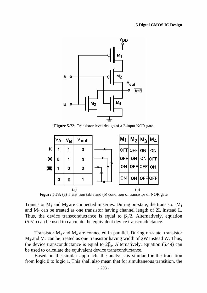
5 Digtal CMOS IC Design
- 203 -
Figure 5.72: Transistor level design of a 2-input NOR gate
(a) (b)
Figure 5.73: (a) Transition table and (b) condition of transistor of NOR gate
Transistor M1 and M2 are connected in series. During on-state, the transistor M1 and M2 can be treated as one transistor having channel length of 2L instead L. Thus, the device transconductance is equal to βp/2. Alternatively, equation (5.51) can be used to calculate the equivalent device transconductance.
Transistor M3 and M4 are connected in parallel. During on-state, transistor M3 and M4 can be treated as one transistor having width of 2W instead W. Thus, the device transconductance is equal to 2βn. Alternatively, equation (5.49) can be used to calculate the equivalent device transconductance.
Based on the similar approach, the analysis is similar for the transition from logic 0 to logic 1. This shall also mean that for simultaneous transition, the

5 Digtal CMOS IC Design
- 204 -
NOR gate can be treated as inverter that has device transconductance parameter βp/2 and 2βn respectively for p-MOS and n-MOS transistors. From mid-point voltage equation (5.23), the mid-point voltage of NOR gate during simultaneous input transition is
VM =
2/
21
V2/
2|V|V
p
n
tnp
ntpDD
ββ
+
ββ+−
(5.60)
The result shows that there is a shift of VM toward the left side of inverter’s VTC curve since VM is smaller.
The graphs in Fig. 5.75 show the plots of voltage characteristic curves for NOR gate, NAND gate, and NOT gate.
Figure 5.74: VTC plot of NOR gate, NAND gate and NOT gate
Consider the NOR gate transistor circuit shown in Fig. 5.75, the output capacitance Cout is equal to Cout = CFET + CL, where CFET is equal to 2CDn + CDp and CL is the load capacitance.

5 Digtal CMOS IC Design
- 205 -
Figure 5.75: NOR circuit for transient response calculation
The reason that CFET is equal to 2CDn + CDp is based on worst case scenario. Since transistor M3 and M4 are connected in parallel, the worst case capacitance is 2CDn. Since transistor M1 and M2 are connected in series than the worst case capacitance is CDp.
The channel resistances of n-MOS and p-MOS transistors are respectively
equal to Rn = )VV(
1
tnDDn −β and Rp =
|)V|V(
1
tpDDp −β.
During the charging of Cout capacitance charges from 0 volt to VDD volt, the
output voltage Vout is equal to Vout = VDD[1- exp(-t/τp)] (5.61)
The time constant τp is equal to 2RpCout + RpCY, which has the worst case channel resistance equal to 2Rp. CY is the inter transistor capacitance of p-MOS transistor. CY is usually equal to the sum of CDp of transistor M1 and CSp of transistor M2. Thus, the tr rise time is tr = 2.2Rp(2CFET + CY + 2CL) (5.62)

5 Digtal CMOS IC Design
- 206 -
or tr = 2.2Rp(2CFET + CY + 2CL) = t0 + α0CL (5.63) where t0 = 2.2RP(2CFET +CY) is the non load rise time and α0 is equal to 4.4Rp.
During the discharging of Cout capacitance discharges from VDD volt to 0 volt, the output voltage Vout is equal to
Vout = VDDexp(-t/τn) (5.64)
According to circuit shown in Fig. 5.75, the time constant τn is given by τn = RnCout. The fall time tf is then given by tf = 2.2τn = 2.2RnCout (5.65) or tf = 2.2τn = t1 + α1CL (5.66) where t1 = 2.2RnCFET and α1 = 2.2Rn.
5.13 Power Dissipation of NOT Gate The power dissipation of the NOT gate shall be analyzed in this Section. There are two types of power dissipation associated with CMOS circuit. They are static power dissipation PDC and dynamic power dissipation Pdyn. When the circuit is not in operation the power dissipation is known as static power dissipation PDC. When it is in operation, it is known as dynamic power dissipation Pdyn. Thus, for a NOT gate, the static power dissipation is equal to PDC = VDDIDD. Based on the voltage characteristic curve shown in Fig. 5.66 and the drain current plot shown in Fig. 5.76, the output of the NOT gate is either at logic 1 or logic 0, whereby in both cases, one of the MOS transistor is at cutoff. Since the p-MOS transistor is connected in series with n-MOS transistor, theoretically, there is no power dissipation at static condition. However, due to sub-threshold conduction and other leakage associated with the design, there is a small amount of current in pico-ampere per gate. This current is termed as quiescent leakage current IDDQ. Thus, static power dissipation is PDC = VDDIDDQ. One has to take note that during the transition of the output voltage either changing from logic 1 to logic 0 or from logic 0 to logic 1, the maximum dc current consumption occurred when output voltage is equal to input voltage,

5 Digtal CMOS IC Design
- 207 -
which is the mid-point voltage VM of Fig. 5.76 at point 3. At this point, both p-MOS and n-MOS transistors are in saturation mode. It is obvious to say the maximum current drain occurred when the both n-MOS and p-MOS transistors are connected in series are in saturation mode. The dynamic power dissipation Pdyn can be calculated with the charging and discharging figure shown in Fig. 5.77.
Figure 5.76: The drain current versus input voltage of the NOT gate at different mode of
operation The output is charged to VDD during transition to logic 1 and discharged to logic 0 during transition to logic 0. The sum of charging and discharging time is considered as equal to the period T of the input frequency. Thus, the dynamic current iDD is equal to Q/T, where Q is the charge of output capacitor Cout, which is also equal to VDDCout. The dynamic power Pdyn is equal to
Pdyn = VDDiDD = VDDT
Q = Cout f2DDV (5.67)
(a) Input voltage (b) Charging output capacitance Cout (c) Discharging output capacitance
Cout Figure 5.77: Charging and discharging circuits of a NOT gate

5 Digtal CMOS IC Design
- 208 -
After adding the static power PDC, the total power dissipation PD of the NOT gate is PD = VDDIDDQ + Cout f2
DDV (5.68)
5.14 Power Dissipation of Complex Logic Gate The total power dissipation PD of the logic gate is PD = VDDIDDQ + Cout f2
DDV after ignoring the short circuit power dissipation. Since the static power VDDIDDQ is small as compared to the dynamic power. Therefore, power dissipation of logic gate is basically come from dynamic power. Dynamic power is power consumption resulted from transistor switching from logic 0 to logic 1 and from logic 1 to logic 0. For a complex logic circuit that has many transitions and if we assume that there are equal chance of transition from logic 0 to logic 1 and vice versa, then we can introduce the term activity coefficient a, which is the product of probability p0 of transition from logic 0 to logic 1 and p1 the probability of transition from logic 1 to logic 0. Thus, activity coefficient is a = p0p1. The power dissipation of a gate can be written as PD = aCout f2
DDV (5.69) Take for an example, a 2-input NOR has three logic 0 output and one logic 1
output, the activity coefficient is a = 16
3
4
1
4
3 =⋅ . However, most of the digital
system shows that the maximum activity coefficient is 0.5. Thus, in general equation (5.69) can be re-written as Pdyn = 0.5Cout f2
DDV (5.70)
For a complex circuit that contains N complex gate, the total power dissipation after ignoring static power dissipation is equal to
PD = ∑=
N
1iDDiii VVCa f (5.71)
or
PD = ∑=
N
1iDDii VVC5.0 f (5.72)
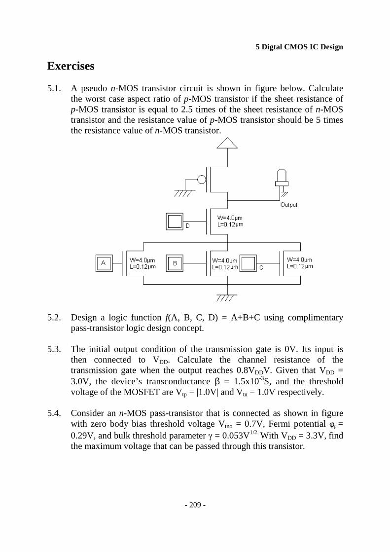
5 Digtal CMOS IC Design
- 209 -
Exercises 5.1. A pseudo n-MOS transistor circuit is shown in figure below. Calculate
the worst case aspect ratio of p-MOS transistor if the sheet resistance of p-MOS transistor is equal to 2.5 times of the sheet resistance of n-MOS transistor and the resistance value of p-MOS transistor should be 5 times the resistance value of n-MOS transistor.
5.2. Design a logic function f(A, B, C, D) = A+B+C using complimentary pass-transistor logic design concept.
5.3. The initial output condition of the transmission gate is 0V. Its input is
then connected to VDD. Calculate the channel resistance of the transmission gate when the output reaches 0.8VDDV. Given that VDD = 3.0V, the device’s transconductance β = 1.5x10⁻³S, and the threshold voltage of the MOSFET are Vtp = |1.0V| and Vtn = 1.0V respectively.
5.4. Consider an n-MOS pass-transistor that is connected as shown in figure
with zero body bias threshold voltage Vtno = 0.7V, Fermi potential Fφ = 0.29V, and bulk threshold parameter γ = 0.053V1/2. With VDD = 3.3V, find the maximum voltage that can be passed through this transistor.

5 Digtal CMOS IC Design
- 210 -
5.5. Design a 4-to-1 MUX using transmission gate.
5.6. Design the transistor level circuit for a 1-to-4 de-multiplexer circuit.
5.7. Design an exclusive NOR gate using transmission gate.
5.8. From the circuit shown below, what is the logic function at output 1 and output 2?
5.9. Design a logic function f(A, B, C, D) = DCBA ++⋅ with at least two
transmission gates. 5.10. What is the difference between a combinational logic circuit and a
sequential circuit?

5 Digtal CMOS IC Design
- 211 -
5.11. Given a CMOS inverter has Wn = 20µm, Lp = Ln = 2µm, Kp = 2.0x10⁻⁵A/V2, Kn = 5.0x10⁻⁵A/V2, find the value of the gate width Wp for βp = βn.
5.12. Calculate the switching point of a CMOS inverter if βn = 1.5βp, Vtn = |Vtp|
= 0.7V, VDD = 5.0V, Kn = 2.5Kp, Ln = Lp = 1.0µm.
5.13. Consider an n-MOS transistor that has a channel width W = 8µm, a channel length of L = 0.5µm and is made with a process where Kn = 180x10-6A/V2, Vtn = 0.70V and VDD = 3.3V. Calculate the channel resistance.
5.14. A complex CMOS logic function is f(A, B, C, D) = )DC(BA ++ . Find the
aspect ratio of each MOS transistor such that the gate delay is not worse than that of a basic CMOS inverter, which have aspect ratio 1.5 and 5 respectively for n-MOS and p-MOS transistor for 0.12µm technology.

5 Digtal CMOS IC Design
- 212 -
Bibliography 1. John P. Uyemura, “Chip Design for Submicron VLSI: CMOS Layout and
Simulation”, Thomson, 2006. 2. John P. Uyemura, “Introduction to VLSI Circuits and Systems”, John
Wiley & Sons, Inc. 2002. 3. Etienne Sicard and Sonia Delmas Bendhia, “Basics of CMOS Cell
Design”, TATA McGraw Hill, 2006. 4. Sung-Mo Kang and Yusuf Leblebici, “CMOS Digital Integrated Circuits
Analysis and Design”, third edition, McGraw Hill, 2005.