1 5-bit decimation filter loretta chui, xiao zhuang hock cheah, gita kazemi advisor: david parent...
Post on 22-Dec-2015
214 views
TRANSCRIPT

1
5-bit Decimation Filter
Loretta Chui, Xiao ZhuangHock Cheah, Gita Kazemi
Advisor: David ParentDecember 6, 2004

2
Agenda• Abstract• Introduction• Project Details• Results• Cost Analysis• Conclusions

3
Abstract
• We designed a 5-bit Decimation Filter, which can be used to sample the output of an A/D converter at a lower rate. Our system operates at 143 MHz, uses less than 100 mW of power, and occupies an area of 360 x 280 m2.

4
Introduction
• The averaging filter used at the output of an A/D converter is called a decimation filter.
• The decimation filter samples the incoming data until the sum of k inputs has been accumulated. Then, the sum is dumped into an output flip-flop. Through this process, the filter reduces (decimates) the output frequency by k times.

5

6
Longest Path Calculationsfor the 7-bit Adder
nsns
PHL 28.18
5
C E L L B it # W N W P C g o r C in p h l A S N S N N S P N M R W N W PL o a d ( c m ) L o a d ( c m ) ( o f lo a d ) F ( = tp lh ) s c m c m
I N V 7 G i v e n G i v e n 2 .0 E - 1 4 2 .1 E - 1 0 1 .2 E + 0 4 1 1 1 1 1 1 .8 8 .8 E - 0 5 1 .6 E - 0 4A O I _ S U M 7 8 .8 E - 0 5 1 .6 E - 0 4 4 .1 E - 1 5 2 .1 E - 1 0 1 .2 E + 0 4 1 2 2 4 2 1 .8 2 .8 E - 0 4 4 .9 E - 0 4
A O I _ C 7 2 .8 E - 0 4 4 .9 E - 0 4 1 .3 E - 1 4 2 .1 E - 1 0 1 .2 E + 0 4 1 2 2 4 2 1 .8 5 .0 E - 0 4 8 .9 E - 0 4I N V _ C 6 5 .0 E - 0 4 8 .9 E - 0 4 4 .7 E - 1 4 2 .1 E - 1 0 1 .2 E + 0 4 1 1 1 1 1 1 .8 1 .9 E - 0 4 3 .5 E - 0 4A O I _ C 6 1 .9 E - 0 4 3 .5 E - 0 4 9 .1 E - 1 5 2 .1 E - 1 0 1 .2 E + 0 4 1 2 2 4 2 1 .8 4 .0 E - 0 4 7 .2 E - 0 4I N V _ C 5 4 .0 E - 0 4 7 .2 E - 0 4 3 .7 E - 1 4 2 .1 E - 1 0 1 .2 E + 0 4 1 1 1 1 1 1 .8 1 .6 E - 0 4 2 .8 E - 0 4A O I _ C 5 1 .6 E - 0 4 2 .8 E - 0 4 7 .4 E - 1 5 2 .1 E - 1 0 1 .2 E + 0 4 1 2 2 4 2 1 .8 3 .6 E - 0 4 6 .4 E - 0 4I N V _ C 4 3 .6 E - 0 4 6 .4 E - 0 4 3 .4 E - 1 4 2 .1 E - 1 0 1 .2 E + 0 4 1 1 1 1 1 1 .8 1 .4 E - 0 4 2 .5 E - 0 4A O I _ C 4 1 .4 E - 0 4 2 .5 E - 0 4 6 .6 E - 1 5 2 .1 E - 1 0 1 .2 E + 0 4 1 2 2 4 2 1 .8 3 .4 E - 0 4 6 .1 E - 0 4I N V _ C 3 3 .4 E - 0 4 6 .1 E - 0 4 3 .2 E - 1 4 2 .1 E - 1 0 1 .2 E + 0 4 1 1 1 1 1 1 .8 1 .4 E - 0 4 2 .4 E - 0 4A O I _ C 3 1 .4 E - 0 4 2 .4 E - 0 4 6 .3 E - 1 5 2 .1 E - 1 0 1 .2 E + 0 4 1 2 2 4 2 1 .8 3 .3 E - 0 4 5 .9 E - 0 4I N V _ C 2 3 .3 E - 0 4 5 .9 E - 0 4 3 .1 E - 1 4 2 .1 E - 1 0 1 .2 E + 0 4 1 1 1 1 1 1 .8 1 .3 E - 0 4 2 .4 E - 0 4A O I _ C 2 1 .3 E - 0 4 2 .4 E - 0 4 6 .2 E - 1 5 2 .1 E - 1 0 1 .2 E + 0 4 1 2 2 4 2 1 .8 3 .3 E - 0 4 5 .9 E - 0 4I N V _ C 1 3 .3 E - 0 4 5 .9 E - 0 4 3 .1 E - 1 4 2 .1 E - 1 0 1 .2 E + 0 4 1 1 1 1 1 1 .8 1 .3 E - 0 4 2 .3 E - 0 4A O I _ C 1 1 .3 E - 0 4 2 .3 E - 0 4 6 .1 E - 1 5 2 .1 E - 1 0 1 .2 E + 0 4 1 2 2 4 2 1 .8 3 .3 E - 0 4 5 .8 E - 0 4

7
Longest Path Calculationsfor the D-Flipflops
F i r s t D F F M + N S P S N t p h l C g W n W p C lo a dN O R 2 f o r s la v e 5 2 1 3 .3 0 E - 1 0 2 .5 4 E - 1 4 3 .7 4 E - 0 4 1 .3 1 E - 0 3 2 .8 8 E - 1 4K e e p e r f o r s la v e N / A N / A N / A 3 .3 0 E - 1 0 N / A 1 .5 0 E - 0 4 1 .5 0 E - 0 4 5 .4 0 E - 1 5D r iv e r f o r s la v e 5 2 2 3 .3 0 E - 1 0 2 .8 8 E - 1 4 3 .2 9 E - 0 4 5 .7 5 E - 0 4 1 .5 4 E - 1 4N O R 2 f o r m a s t e r 5 2 1 3 .3 0 E - 1 0 2 .0 8 E - 1 4 3 .1 2 E - 0 4 1 .0 9 E - 0 3 2 .4 0 E - 1 4K e e p e r f o r m a s t e r N / A N / A N / A 3 .3 0 E - 1 0 N / A 1 .5 0 E - 0 4 1 .5 0 E - 0 4 5 .4 0 E - 1 5D r iv e r f o r m a s t e r 5 2 2 3 .3 0 E - 1 0 2 .4 0 E - 1 4 2 .7 8 E - 0 4 4 .8 6 E - 0 4 1 .3 0 E - 1 4
S e c o n d D F F M + N S P S N t p h l C g W n W p C lo a dN O R 2 f o r s la v e 5 2 1 3 .3 0 E - 1 0 3 .0 8 E - 1 4 4 .4 7 E - 0 4 1 .5 6 E - 0 3 3 .4 4 E - 1 4K e e p e r f o r s la v e N / A N / A N / A 3 .3 0 E - 1 0 N / A 1 .5 0 E - 0 4 1 .5 0 E - 0 4 5 .4 0 E - 1 5D r iv e r f o r s la v e 5 2 2 3 .3 0 E - 1 0 3 .4 4 E - 1 4 3 .8 8 E - 0 4 6 .7 8 E - 0 4 1 .8 2 E - 1 4N O R 2 f o r m a s t e r 5 2 1 3 .3 0 E - 1 0 2 .3 6 E - 1 4 3 .5 0 E - 0 4 1 .2 2 E - 0 3 2 .6 9 E - 1 4K e e p e r f o r m a s t e r N / A N / A N / A 3 .3 0 E - 1 0 N / A 1 .5 0 E - 0 4 1 .5 0 E - 0 4 5 .4 0 E - 1 5D r iv e r f o r m a s t e r 5 2 2 3 .3 0 E - 1 0 2 .6 9 E - 1 4 3 .0 9 E - 0 4 5 .4 0 E - 0 4 1 .4 5 E - 1 4
8
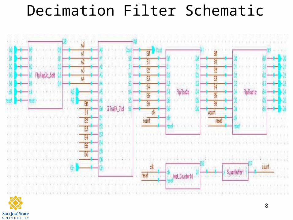
Decimation Filter Schematic

9
System Counter

10
Decimation Filter Layout

11
LVS Verification

12
Simulations (schematic)

13
Simulations (extracted)
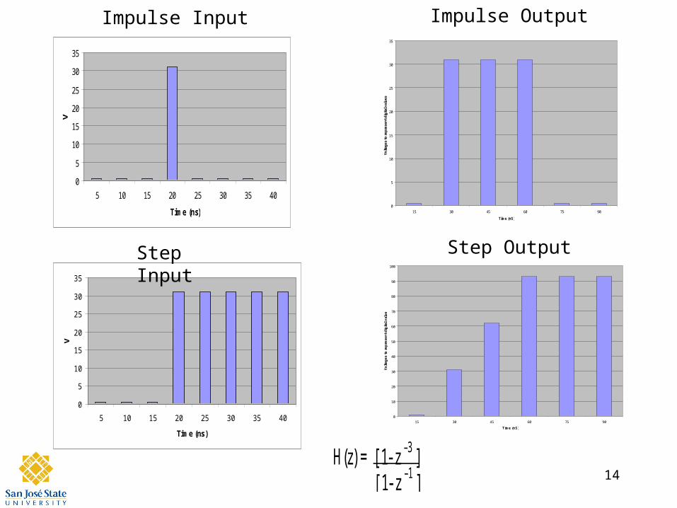
14
Impulse Input
0
5
10
15
20
25
30
35
15 30 45 60 75 90
Time (nS)
Volta
ges
to r
epre
sent
dig
ital v
alue
s
0
10
20
30
40
50
60
70
80
90
100
15 30 45 60 75 90
Time (nS)
Vo
ltag
es
to r
ep
rese
nt
dig
ital
val
ue
s
0
5
10
15
20
25
30
35
5 10 15 20 25 30 35 40
Time (ns)
V
0
5
10
15
20
25
30
35
5 10 15 20 25 30 35 40
Time (ns)
V
Impulse Output
Step Input Step Output
H(z) = [ 1- z –3 ][ 1- z –1 ]

15
DFF Rise Time For Hold DFF Fall Time For Hold

16
DFF Rise Time for Setup DFF Fall Time for Setup

17
Power Waveform

18
Cost Analysis
• Estimated time spent on each phase of the project:– verifying logic (1 week)– verifying timing (1 week)– layout (3 weeks)– post extracted timing (1.5 weeks)

19
Conclusion
• We designed a decimation filter, which samples and sums the incoming data 3 inputs at a time. Through this process, the filter reduces (decimates) the output frequency by a factor of 3.
• Our design met all specifications except for timing because our adder was too slow.
• We propose the use of an alternative design, which uses a mux select to implement a faster adder.

20
Alternative Adder using a Mux Select

21
Lessons Learned
• It would be helpful to students to use a layered approach for the chip layout by creating instances of individual parts instead of copy and paste to improve debugging capabilities.
• It would be helpful if professors could spend some time to cover testing methodology.

22
Acknowledgements
• Thanks to our family and friends who missed us for the past 3 months.
• Thanks to Cadence Design Systems for the VLSI lab.
• Thanks to Dr. Parent and John for their advice and great patience.