1 cmos latchup
TRANSCRIPT
1 CMOS Latchup
1.1 CMOS LATCHUP
Latchup!
In this chapter, a brief overview of latchup is provided. We will provide a first quick look on what
latchup is. As a starting point, this discussion will be followed by a summary of evolution, history, key
innovations and patents. This chapter discusses the key innovations, contributions and patents
associated with the process of understanding how to address the latchup issue in semiconductor
technology. In addition, this chapter will provide the reader what are the sources of latchup, from
pulses to particles; latchup issues associated with ionizing radiation events, as well as current and
voltage excursions outside of the native current and voltage conditions of a technology, will be shown.
In this discussion, the issue of technology scaling and how scaling leads to latchup concerns will be
reviewed. When this chapter is completed, the following chapters will spiral backward into more depth,
on each individual area from models, testing and tools.
1.1.1 CMOS Latchup–What is Latchup?
Latchup is a state where a semiconductor device undergoes a high-current state as a result of interaction
between a pnp and an npn bipolar transistor. The pnp and npn transistors can be natural to the
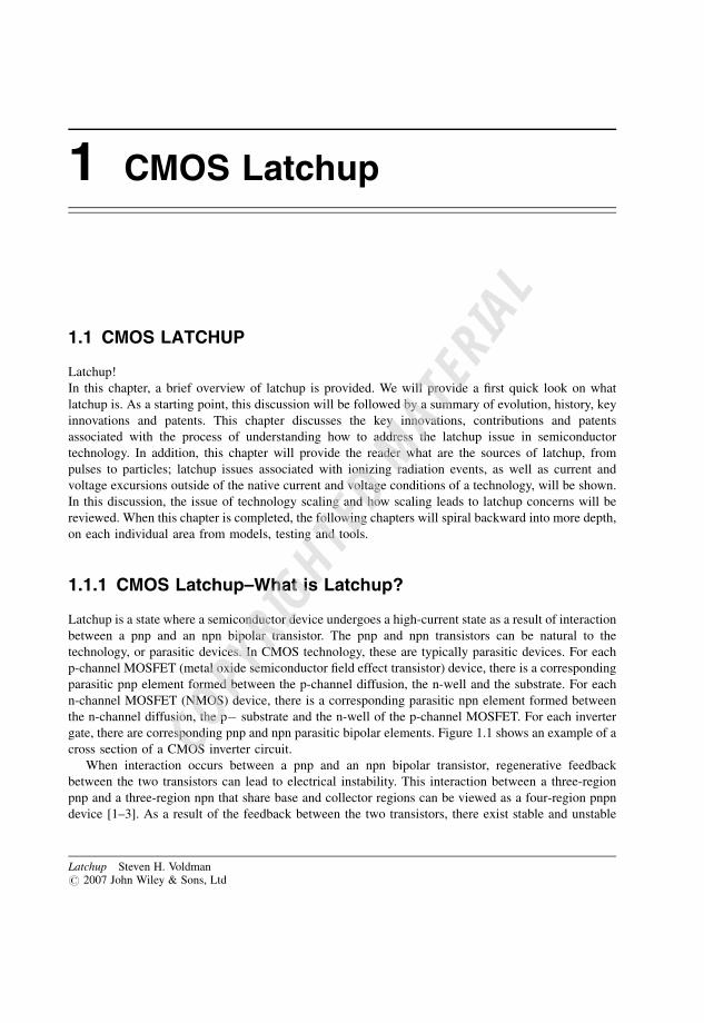
technology, or parasitic devices. In CMOS technology, these are typically parasitic devices. For each
p-channel MOSFET (metal oxide semiconductor field effect transistor) device, there is a corresponding
parasitic pnp element formed between the p-channel diffusion, the n-well and the substrate. For each
n-channel MOSFET (NMOS) device, there is a corresponding parasitic npn element formed between
the n-channel diffusion, the p substrate and the n-well of the p-channel MOSFET. For each inverter
gate, there are corresponding pnp and npn parasitic bipolar elements. Figure 1.1 shows an example of a
cross section of a CMOS inverter circuit.
When interaction occurs between a pnp and an npn bipolar transistor, regenerative feedback
between the two transistors can lead to electrical instability. This interaction between a three-region
pnp and a three-region npn that share base and collector regions can be viewed as a four-region pnpn
device [1–3]. As a result of the feedback between the two transistors, there exist stable and unstable
Latchup Steven H. Voldman# 2007 John Wiley & Sons, Ltd
COPYRIG
HTED M
ATERIAL
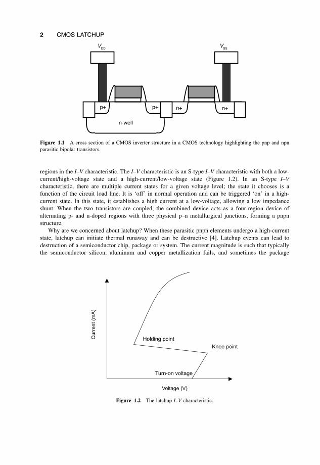
regions in the I–V characteristic. The I–V characteristic is an S-type I–V characteristic with both a low-
current/high-voltage state and a high-current/low-voltage state (Figure 1.2). In an S-type I–V
characteristic, there are multiple current states for a given voltage level; the state it chooses is a
function of the circuit load line. It is ‘off’ in normal operation and can be triggered ‘on’ in a high-
current state. In this state, it establishes a high current at a low-voltage, allowing a low impedance
shunt. When the two transistors are coupled, the combined device acts as a four-region device of
alternating p- and n-doped regions with three physical p–n metallurgical junctions, forming a pnpn
structure.
Why are we concerned about latchup? When these parasitic pnpn elements undergo a high-current
state, latchup can initiate thermal runaway and can be destructive [4]. Latchup events can lead to
destruction of a semiconductor chip, package or system. The current magnitude is such that typically
the semiconductor silicon, aluminum and copper metallization fails, and sometimes the package
VSSVDD
p+
n-well
p+ n+ n+
Figure 1.1 A cross section of a CMOS inverter structure in a CMOS technology highlighting the pnp and npn
parasitic bipolar transistors.
Holding point
Turn-on voltage
Knee point
Figure 1.2 The latchup I–V characteristic.
2 CMOS LATCHUP
materials melt. Note that another indicator of latchup is the package cracking, melting, delamination,
separation and outgassing. Another clear indicator, on a system level, is smoke. In these cases, it is
difficult to provide chip-level failure analysis due to the magnitude of the package and system damage.
When the card smoke is evident, the module package is melted and the silicon chip is molten, this is a
good indicator that latchup has occurred in your semiconductor chip.
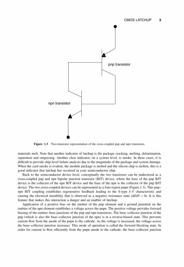
Back to the semiconductor device level, conceptually the two transistors can be understood as a
cross-coupled pnp and npn bipolar junction transistor (BJT) device, where the base of the pnp BJT
device is the collector of the npn BJT device and the base of the npn is the collector of the pnp BJT
device. The two cross-coupled devices can be represented as a four-region pnpn (Figure 1.3). This pnp–
npn BJT coupling establishes regenerative feedback leading to the S-type I–V characteristic and
causing the electrical instability that is observed as a negative resistance state (dI/dV < 0). It is this
feature that makes this interaction a danger and an enabler of latchup.
Application of a positive bias on the emitter of the pnp element and a ground potential on the
emitter of the npn element establishes a voltage across the pnpn. The positive voltage provides forward
biasing of the emitter–base junctions of the pnp and npn transistors. The base–collector junction of the
pnp (which is also the base–collector junction of the npn) is in a reverse-biased state. This prevents
current flow from the anode of the pnpn to the cathode. As the voltage is increased, the voltage across
the base–collector junction increases. This mode of operation is called the forward blocking state. In
order for current to flow efficiently from the pnpn anode to the cathode, the base–collector junction
pnp transistor
npn transistor
Figure 1.3 Two-transistor representation of the cross-coupled pnp and npn transistors.
CMOS LATCHUP 3
must allow current to flow. For current continuity at the cross-coupled nodes, the collector current of
the pnp transistor must equal the base current of the npn transistor, as well as the collector current of
the npn transistor must equal the base current of the pnp transistor. Mathematically, the coupling is
established through solving Kirchoff’s current law at the base–collector nodes. In this form, the
standard equations of bipolar transistors can be used to quantify the interaction and current in the pnpn
structure. Hence, the two nodal equations can be expressed as
Icp ¼ Ibn;
Icn ¼ Ibp;
where Icp and Icn are the collector currents of the pnp and npn bipolar junction transistors, respectively,
and likewise, Ibn and Ibp are the base currents of the npn and pnp bipolar junction transistors,
respectively. The total current through the pnpn structure is equal to the emitter current of the pnp or
npn bipolar transistor, Iep and Ien, respectively. From Kirchoff’s current law in the transistor, the emitter
current must equal the sum of the base and collector currents:
I ¼ Iep ¼ Icp þ Ibp:
From the coupling relationships, the current can be expressed as
I ¼ Iep ¼ Icp þ Icn ¼ Ibp þ Ibn ¼ Icn þ Ibn ¼ Ien ¼ I:
Solving for the current as a function of the two collector current relationships, the collector current can
be represented as a function of the emitter current:
Icp ¼ aIep þ Icp0;
Icn ¼ aIen þ Icn0;
where the collector current is equal to the product of the collector-to-emitter transport factor a and the
emitter current summedwith the base–collector leakage. Solving for the current through the pnpn structure,
I ¼ Icp0 þ Icn0
1 ðan þ apÞ :
From this analysis, it is clear that the current is infinite, when the denominator is equal to zero. This
condition can be expressed as
ap þ an ¼ 1:
This expression shows that when the sum of the collector-to-emitter gains is equal to unity, the current
goes to infinity. This can also be expressed as a function of the bipolar transistor current gain b,substituting in for the collector–emitter transport,
I ¼ Icp0 þ Icn0
1 bnbn þ 1
þbp
bp þ 1
! ;
where
an ¼bn
bn þ 1;
ap ¼bp
bp þ 1:
4 CMOS LATCHUP
In this form, when the denominator is equal to zero, the product of the bipolar current gains is equal to
unity:
bnbp ¼ 1:
The pnpn current magnitude can be large given that the numerator is large, or if the denominator
approaches zero.
Hence, from a simple derivation, it can be observed that the regenerative feedback between
the parasitic pnp and the npn has a condition where a large current can be established between
the power supply and the ground rail in an inverter circuit through the parasitics associated with the
p- and the n-channel MOSFET transistor. The transport properties of the parasitic pnp and the npn
are also involved, which are influenced by the semiconductor process and the chip design layout. As
a result, latchup involves the chip architecture, the circuit layout, the circuit design and the
semiconductor process.
What is the frequency of these parasitics in a modern semiconductor design? Today, in an advanced
CMOS microprocessor with 200 million transistors, there are 100 million p-channel MOSFETs and
100 million n-channel MOSFETs. As a result, there are 100 million pnp and 100 million npn
transistors. Hence, there are on the order of 100 million pnpn elements in a CMOS logic chip that
contains 100 million inverter circuits.
Question: How many circuits does it take to initiate CMOS latchup? Answer: One.
As the number of circuits increases, the number of peripheral circuits and I/O circuits increases. In a
CMOS chip with 200 million transistors, there may be on the order of 1000–10 000 interface circuits. It
is likely that voltage and current events on the interface circuits can lead to latchup.
Question: How many peripheral circuits does it take to initiate CMOS latchup? Answer: One.
Yet, today, the number of products exhibiting latchup is a small minority of designs and
applications. Hence, there must be a method or methods to diagnose and discriminate which parasitic
pnpn structures are important, and which are not. Additionally, there are semiconductor process
solutions, circuit solutions and system solutions.
1.1.2 CMOS Latchup–Why is Latchup Still an Issue ?
A key question on CMOS latchup is the following–Why is latchup still a concern? There are many
reasons why latchup is an issue in today’s semiconductor chips. The reasons why is is a concern in
some corporations differ based on the choices made in the semiconductor technology, latchup design
strategy as well as the latchup methodology. The following is a list of why this issue reoccurs
in semiconductor chips:
lack of characterization of parasitic devices;
lack of semiconductor process control of parasitic devices;
lack of dc and ac models of parasitic devices;
lack of parasitic devices in the circuit simulation;
lack of extraction, checking and verification of parasitic devices;
lack of tools addressing parasitic devices between devices, circuits and subfunctions;
lack of ground rules that sufficiently provide 100 % coverage of design environment;
CMOS LATCHUP 5
low business priority of addressing CMOS latchup, until it is a concern;
lack of educational training on CMOS latchup in university and college course work for circuit and
layout design engineers and technicians;
education focus on the understanding of bipolar transistors and parasitic transistors;
lack of focus on latchup during semiconductor process and device design point definition;
lack of preservation of dimensional and electrical similitude of the lateral and vertical dimensions in
the scaling of CMOS technology;
lack of awareness of the CMOS latchup technology scaling and making CMOS latchup technology
part of the technology roadmap;
lack of semiconductor device and CMOS latchup design point cosynthesis;
isolation, well and substrate scaling;
new design methodologies in digital, mixed signal and RF designs;
nonnative voltages integrated into products well above the native-voltage CMOS latchup capability;
introduction of high-voltage CMOS (HVCMOS) integrated with low-voltage CMOS (LVCMOS)
circuitry;
new issues associated with subsystem and system integration;
reversal of battery installation;
negative polarity on pins;
wire-bond mismatching in multichip power systems.
These are just some of the reasons why today CMOS latchup is not ‘cured’ and remains an issue in
today’s semiconductor chips. In this book, we will address many of these issues in the following
chapters.
1.1.3 Early CMOS Latchup History
The first transistor, invented at Bell Labs in 1947, was not a CMOS transistor, but was a bipolar
junction transistor device. At that time, an advantage of the bipolar junction transistor was the
ability to manufacture it, as well as the speed of the transistor. One of the early advantages of the
bipolar junction transistor was that it was not a surface device, but a bulk device. In 1955, Bell Labs
manufactured and demonstrated the first metal oxide semiconductor field effect transistor. The
MOSFET structure was proposed in 1930 by Lilienfeld [5] and Heil [6], but was not manufactured
successfully due to fixed and mobile positive charge issues. Fixed charge and mobile charge
problems also remained a large issue in p-channel transistors, leading to the early implementation of
n-channel MOSFET technology. CMOS had to wait for the p-channel MOSFET device to emerge
while the development and research community continued to look for a solution to the oxide charge
problem.
By the late 1960s, many manufacturers offered integrated circuits based on either a p-channel or an
n-channel MOSFET device. CMOS was invented by RCA and was first demonstrated by Al Medwin at
RCA’s technology center in Somerville, New Jersey. The RCA Corporation called this technology
6 CMOS LATCHUP
COS/MOS, which stood for complementary symmetry metal oxide silicon. The first circuits using
COS/MOS included a circuit that contained 13 transistors with a 15-V power supply.
Early interest in CMOS was also due to the potential for military and space applications.
Publications in the 1960s by Kinoshita et al. [7], Poll and Leavy [8, 9] and Dennehy et al. [10]
focused on the initiation of CMOS latchup in radiation environments.
CMOS latchup became of growing interest in the early 1970s as interest increased in the usage of
CMOS for mainstream technology applications. Interest in CMOS continued in Sandia Laboratories
and RCA [11–16]. Gregory and Shafer [12–14], Gallace and Pujol [15] and Barnes et al. [16] of Sandia
Laboratories focused on latchup as an impediment to the mainstream integration of CMOS. During the
first development of RCA’s COS/MOS, CMOS latchup was discovered by Gallace and Pujol [15].
Ironically, the parasitic bipolar transistors unintentionally formed by the CMOS inverter switch
impacted the introduction of CMOS. With the early problems of CMOS technology, most corporations
began to focus on NMOS technology.
In this time frame, prior to mainstream introduction of CMOS, model development, guidelines and
radiation implications were analyzed. Alexander et al. evaluated MOS model implications [17].
Brucker evaluated the implications on CMOS and silicon-on-sapphire (SOS) memory [18]. Coppage
and Evans evaluated the characteristics of the destruction induced by CMOS latchup [19]. Total dose
characterization and other nuclear radiation effects were evaluated by London and Wang [20], Simons
[21] and Ricketts [22].
It was during the late 1970s that the focus on how to improve CMOS latchup using design
techniques and process solutions was first addressed. From a practical perspective, application
guidelines were released by Stephenson to address CMOS latchup guidelines [23]. The focus shifted
toward addressing CMOS latchup by screening, testing and selection processes. Sivo et al. focused on
methods of latchup screening [24]. Crowley et al. used radiation as a method of selection [25, 26]. In
this time frame, the use of neutron irradiation for the prevention of CMOS latchup was proposed by
Adams and Sokel [27]. In this time frame, the use of recombination centers (e.g. using gold dopants)
was demonstrated by Dawes and Derbenwick [28].
In many corporations, the first attempts to establish a mainstream CMOS technology for memory
and logic development discovered the problem of latchup. Early developers of CMOS were hindered
by the latchup problem, impeding the mainstream introduction of CMOS in the 1970s. In those time
frames, MOSFET-based static read access memory (SRAM) introduced resistor-load NMOS cells and
four-device NMOS cells, and avoided integration of p-channel MOSFETs into the network. As a result,
CMOS logic was delayed until solutions to latchup were resolved.
Early CMOS development generations addressed CMOS latchup with the introduction of epitaxial
wafers, guard rings and ground rules. In the late 1970s to early 1980s, early CMOS technologies had
low-doped substrate wafers, recessed oxide (ROX) or LOCOS isolation, and diffused n-wells. These
early CMOS technologies had strong lateral bipolar and vertical bipolar transistors and were latchup
prone. The early work of Estreich et al. [29–33] addressed the physics and modeling of CMOS latchup
to a level suitable for mainstream semiconductor manufacturing. Estreich studied the use of a heavily
doped masked well region, similar to the bipolar subcollector, to improve latchup tolerance.
In the early 1980s, the focus in the CMOS latchup discipline shifted toward the practical integration
of CMOS in manufacturing facilities and mainstream CMOS development. Many of the proposed
concepts prior to this were not acceptable for mainstream CMOS technology (e.g. neutron irradiation
and gold doping). For mainstream implementation of CMOS, it was necessary to understand guard ring
structures, guard ring efficiency, the role of the substrate, semiconductor device models, transient
latchup physics and model development, as well as new process features that could be integrated with
the evolution of CMOS technology.
The works by Dressendorfer and Armendariz [34], Schroder et al. [35], Payne et al. [36] and Raburn
[37] focused on the elimination of CMOS latchup in CMOS technology. Rung et al. [38] and Combs
CMOS LATCHUP 7
[40] discussed the use of p-wells and scaleable p-wells for CMOS integration and for CMOS latchup
improvement. Iizuka and Moll [41] initiated new figures of merit to quantify CMOS latchup. By 1981
and 1982, Dressendorfer and Ochoa [42, 43], Wieder et al. [44], Hu et al. [45], Rung and Momose [46]
and Huang et al. [48] focused on the model development, distribution effects, device simulation and
characterization of CMOS latchup. Troutman and Zappe [49, 50] and Rung and Momose [51] focused
on transient CMOS latchup associated with power-up conditions.
In 1983, the focus was on achieving two goals. Many developers focused on n-well and p-well
optimization for integration with mainstream CMOS. The second goal was to achieve CMOS latchup
‘immunity’. Schwabe et al. [52], Wollesen et al. [53], Goto et al. [54], Hu et al. [55] and the team of
Takacs et al. [56] focused on CMOS n-well and p-well engineering for CMOS technology that was
being cosynthesized with the CMOS latchup objectives for the future 1-mm CMOS technology era.
By 1983, the goal of achieving ‘CMOS latchup immunity’ was being advertised and emphasized for
alleviation of fears of both technology management and customers. During this time frame, latchup
was still prevalent, and the quality of the technologies and the products did not have many of the
proposed solutions that were being proposed in the publications and literature. For example, Manoliu
et al. [57] and Wakeman [58], as well as many other authors, discussed the elimination of CMOS
latchup and CMOS latchup ‘immunity’.
In 1983, the focus continued on the modeling of CMOS latchup. At that time, the focus was on the
improved understanding of guard rings, transient latchup and distribution effects. Troutman focused on
an improved understanding of the guard ring and guard ring efficiency [59]. Niitsu et al. [60] and
Hamdy and Mohsen [61], and G. Hu [63] focused on transient latchup simulation and model
development. With the focus on substrate modeling, distribution effects and better latchup models,
Troutman and Hargrove developed a transmission line model for better quantification of the substrate
on a p epitaxial/pþþ substrate wafer [62]. Research continued in the understanding of CMOS latchup
current paths [64], characterization and test structure development [65] and temperature effects [66].
By 1984, while the research and development publications were being printed, CMOS latchup
technology solutions were being integrated into future semiconductor technologies. Troutman was
responsible for the manufacturing implementation in a 0.8-mm CMOS technology; in this technology
generation, the first high-energy MeV implanter was used for a MeV retrograde well. (Note: it was
integrated into the technology flow prior to 1984, but qualification of the technology did not occur until
1988.) By 1984, the research and development continued toward improved model development [67–78]
as well as a shift in focus on the scaling implications of CMOS latchup [73–75]. Lewis [73], Schwabe
et al. [74] and Odanaka et al. [75] focused on the reduced dimensions and the scaling of the pþ/nþspacings and scaled CMOS.
In this time frame, semiconductor process solutions, characterization and cosynthesis were
integrated into commercial CMOS technologies with significant success. It was believed at this time
that the problem of CMOS latchup was understood and ‘cured’ [79].
It was at this junction that the beginning of the issues of process integration and cosynthesis into
CMOS memory and logic began. In the 1980s, CMOS logic was derived from a DRAM technology
base. In this time frame, the issues of cointegration of CMOS DRAM and logic in a common base led
to CMOS latchup optimization issues that needed to be addressed. In the CMOS IV 4-MB DRAM
technology, Cottrell and Voldman addressed the semiconductor device cointegration of trench DRAM
issues [80]. In this work, it was found that the integration issues associated with DRAM trench parasitic
devices, DRAM retention time and CMOS latchup were all influenced by the n-well design point. The
retrograde well provided a process optimization tool to enhance CMOS latchup immunity. n-well
compensation effects caused by p/pþ substrate wafers in a LOCOS technology were first addressed
by Voldman in 1987 [80]. In 1987, Voldman and Fitzgerald evaluated transient latchup as a function of
retrograde well dose and energy to improve CMOS latchup. In 1991, Voldman evaluated the integration
of retrograde n-well, shallow trench isolation (STI) and epitaxial p/pþþ wafer optimization in
8 CMOS LATCHUP

mainstream 0.5-mm CMOS technology and 16-MB DRAM technology [82]. By 1993, the first 0.25-mm2.5-V CMOS technology integrated solutions for STI and CMOS latchup. After this time frame,
CMOS DRAM development separated from CMOS logic development, leading to the separation of the
two different design points [81–83].
By 1994, the need to achieve good CMOS electrostatic discharge (ESD) protection in CMOS logic
and CMOS microprocessors took precedence over the CMOS latchup design point [82–85]. During this
time frame, the solutions for latchup provided significant CMOS latchup margins. It was found that
with the retrograde well implant process step both excellent ESD protection and latchup robustness
could be achieved as the microprocessors were scaled through successive CMOS technologies [82–86].
In this period, the mainstream technologies also introduced a p-well implant for the n-channel
MOSFET, which improved latchup technology margin.
Between 1995 and 2000, the latchup design point adequately prevented latchup in the majority of
semiconductor applications in memory and logic applications. But, during this time frame, CMOS
technology scaling of the fundamental parameters reduced the latchup margin [87]. Although the
technology latchup robustness prevented latchup from occurring, new computer-aided design (CAD)
methods were needed to integrate I/O design, CMOS latchup and ESD. A shift occurred toward better
design methods, anticipating integration issues in future designs. For example, Li addressed extraction
techniques, peripheral I/O integration and generalized substrate transfer resistance representations
[88, 89]. In this transition period, solutions to address latchup such as heavily doped buried layers
(HDBLs) were proposed, but no evidence of CMOS latchup concerns was evident [91, 92].
Since 2000, with the scaling of technologies from 0.25 mm to 35 nm, mixed signal integration and
the growth of the system-on-chip (SOC), the focus on CMOS latchup has shifted again. During this
time, some of the focus remained on CMOS scaling issues [92, 93]. Morris quantified the scaling
implications of key latchup metrics and process variables for the prediction of future CMOS latchup
concerns [92]. With the increased focus on cost, density, foundry compatibility, mixed signal products,
RF technology and high-level integration (i.e. system-on-a-chip), the environment has significantly
shifted in CMOS integration. Today, advanced CMOS is primarily manufactured on lightly doped
p substrate wafers. Multiple-well technologies require the optimization of isolation structures to
provide the maximum CMOS latchup tolerance. With multiple-well implants, lateral scattering of
implanted ions, multiple-circuit voltages and digital/analog mixed signal chips, the ability to provide a
robust latchup-free technology has once again become a challenge.
During this time, the focus shifted toward CMOS latchup propagation in semiconductor chips,
bipolar CMOS (BiCMOS) process solutions, triple-well CMOS, SOC integration latchup issues, smart
power, high-voltage CMOS and new CAD representations. Latchup propagation, also known as
‘latchup domino effect’ occurred in high-density CMOS chips [94–97]. Weger et al. demonstrated this
using animation techniques of the interaction between ESD networks and CMOS latchup, providing
both spatial and temporal understanding of the CMOS latchup propagation [94]. This work was
extended using CCD camera methods by Stellari [95]. Voldman developed the theory for CMOS
latchup domino effect–addressing both the primary trigger source and the secondary interactions [97].
In the BiCMOS technology, the integrated dense CMOS logic addressed new CMOS latchup process
solutions for wired and wireless applications. Watson and Voldman evaluated the utilization of deep
trench (DT) structures for CMOS latchup improvements as guard rings to bordered n-well structures
[98–102]. The first experimental work on the CMOS latchup robustness of a new low-cost isolation,
known as trench isolation (TI), was also explored for its CMOS latchup advantages [102, 103]. In this
period, triple-well CMOS became important in the technology. Analysis of CMOS ‘merged triple-well’
latchup, where the n-well was interconnected with the buried layer, was also addressed for the first time
[104, 105]. At this time, with the direction of higher substrate resistance, the understanding of the
substrate resistance issue on future technologies is a concern. Voldman demonstrated CMOS latchup in
ultrahigh resistive wafers of 1–5 k cm CMOS substrates [106]. With integration, Salcedo-Suner et al.
CMOS LATCHUP 9
addressed latchup issues within new ESD circuit concepts [107]. With the SOC integration, Huh et al.
addressed new CMOS latchup occurrences between power supplies and between circuits [108].
In addition, more sophisticated methods of CAD extraction and verification using model graph
(MG) representation were pursued by Zhan and Wang [109, 110].
In the background, the smart power technology engineers with bipolar, CMOS and DMOS (BCD)
technology were addressing unique issues in the smart power integration [172–185]. Smart power has
introduced HVCMOS and LVCMOS technologies on a common substrate. HVCMOS technology has
introduced drain-extended NMOS and lateral diffused MOS (LDMOS) technologies at voltage levels
significantly above the CMOS native-voltage power supply. In each successive technology generation
node, the 25-V, 40-V, 100-Vand 120-Vapplications do not scale, whereas LVCMOS continues to lower
its power supply voltage; this leads to a larger voltage difference between HVCMOS and CMOS in
each generation. With smart power and HVCMOS, a larger focus is on injection interaction between
the HVCMOS circuits and LVCMOS; HVCMOS LDMOS injection can lead to disturbing the CMOS
circuitry. As a result, new interdomain passive and active guard ring strategies have been implemented.
Additionally, new niche fields are established that must address CMOS latchup issues. Image
processing semiconductor chips have introduced core-limited designs with the introduction of CMOS
triple-well technology and reintroduction of the p/pþþ substrates and p/nþþ substrates. With the
growth of image chips in cell phones, this area will have growing interest.
It was once believed that latchup would cease to be an issue for advanced technologies as a result of
process solutions, model development, simulation and circuit solutions. Unfortunately, this has turned
out not to be the case. As a result, new latchup solutions from semiconductor process structures,
implants, design tools and circuit solutions still continue to be pursued. In the following chapters, this
will be discussed in more depth.
1.2 FUNDAMENTAL CONCEPTS OF LATCHUP DESIGNPRACTICE
In semiconductor technology, a ‘latchup design practice’ is developed for the analysis of latchup from
semiconductor process to product design. For latchup, there are fundamental latchup design practices
that include semiconductor process, layout design and testing practices. The fundamental concepts and
objectives for the latchup discipline are as follows:
Decoupling of parasitics – spatial separation;
Decoupling of parasitics – physical isolation (triple well);
Decoupling of parasitics – physical isolation (insulating regions);
Recombination and trap states;
Beta spoiling – placement of defects for parasitic bipolar current gain reduction;
Semiconductor doping;
Silicide design;
Isolation design;
Isolation beta spoiling;
Decoupling of parasitics via virtual collector regions;
10 CMOS LATCHUP
Decoupling of parasitics via integrated guard rings;
Separated guard rings;
Shunt well resistors;
Shunt substrate resistors;
Circuit design;
Current-limiting circuit elements;
Power application issues – sequence-independent circuits;
Power application issues – power sequencing with sequence-dependent circuitry;
Current-limiting circuit solutions – external current-limiting circuit elements;
Use of on-chip ESD power clamp networks;
Use of on-chip ESD rail-to-rail networks;
Use of on-chip active clamp networks;
Active guard rings – local substrate potential modulation;
Active guard rings – introduction of substrate lateral electric field;
Active guard rings – inversion of injection;
Active and passive guard ring synthesis;
Failure analysis – photoemission failure analysis techniques;
Failure analysis – particle beam methodology;
Computer-aided design – identification of parasitic elements;
Computer-aided design – inclusion of parasitics in circuit analysis;
Computer-aided design – guard ring implementation;
Computer-aided design – well and contact spacing optimization;
Computer-aided design – latchup contact placement cosynthesis using cost functionals;
Chip architecture – floor planning based on parasitic pnpn.
Decoupling of parasitics – spatial separation: To avoid the interaction between the pnp and the
npn transistor, spatial separation of the parasitic transistors inherently increases the latchup robustness.
Decoupling of parasitics – physical isolation (triple well): To avoid interaction between the pnp and the
npn parasitic transistors, full decoupling can be achieved by physical separation using other structures
between the transistors. Using a triple-well region, one can fully isolate the npn and the pnp transistor
parasitic elements.
Decoupling of parasitics – physical isolation (insulating regions): To avoid interaction between the pnp
and the npn parasitic transistors, isolation can be placed in between. In this case, the isolation can
provide decoupling when the depth of the isolation is significant, and/or fully isolating on the edges as
well as below the structure.
FUNDAMENTAL CONCEPTS OF LATCHUP DESIGN PRACTICE 11
Recombination centers and trap states: To avoid interaction between the pnp and the npn parasitic
transistors, recombination centers and trap states can be added to the base region of the pnp and/or npn
transistor. Recombination centers and trap states can be generated in the bulk region (e.g. bulk
recombination centers) or on surfaces (e.g. surface recombination centers). Recombination centers can
be generated by implantation damage, implanted impurities or irradiation. Recombination centers can
be neutral or charged centers.
Beta spoiling – placement of defects for parasitic bipolar current gain reduction: To avoid interaction
between the pnp and the npn parasitic transistors, defects and trap states can be added to the base region of
the pnp and/or npn transistor. Defects can be generated in the bulk region (e.g. bulk recombination centers)
or on surfaces (e.g. surface recombination centers). Recombination centers can be generated by implanta-
tion damage, implanted impurities or irradiation. Recombination centers can be neutral or charged centers.
Semiconductor doping – high doping concentration: The semiconductor region can be doped in order
to reduce the bipolar current gain through reduction in the minority carrier diffusion length. This can be
achieved by reduction in both recombination time and minority carrier mobility.
Silicide design: The silicide design is established to introduce resistance in the emitter regions. Emitter
resistance leads to a reduction in the regenerative feedback and improves the latchup robustness. In the
latchupdesign practice, the introduction of emitter resistance is a technique to increase the latchup robustness.
Isolation design: The semiconductor isolation design can be optimized to improve the latchup
robustness of the semiconductor technology. Isolation structures can include STI, dual-depth (DD)
STI, TI and DT isolation structures.
Isolation beta spoiling: It is a latchup design practice for the degradation of the parasitic bipolar
transistors’ current gain by influencing the isolation surfaces. These can include surface state
generation, defect generation or channel stop implants. Additional methods under isolation are
provided to lower the bipolar current gain transport along the isolation edges.
Decoupling of parasitics via virtual collector regions: It is a latchup design practice to add a virtual
collector region. By the addition of a virtual collector region, minority carriers can be collected
lowering the regenerative feedback between the sources of the parasitic pnpn. With the introduction of
a virtual collector, the bipolar current gain of either the pnp or the npn is lowered, which improves the
latchup robustness. These virtual collector structures can be vertical or lateral elements.
Decoupling of parasitics via integrated guard rings: It is a latchup design practice to add an integrated
guard ring to serve as a virtual collector. Minority carriers can be collected lowering the regenerative
feedback between the sources of the parasitic pnpn.
Decoupling of parasitics via separated guard rings: It is a latchup design practice to add a separated guard
ring to serve as a virtual collector. By a separate region, minority carriers can be collected lowering the
regenerative feedback between the sources of the parasitic pnpn. The separate guard ring structures can be
placed lateral or vertical and lead to a loss of the current lowering the bipolar current gain.
Shunt well resistors: It is a latchup design practice to provide low-resistance well shunts in parallel with
the emitter–base metallurgical junction of the parasitic element contained within the well structure.
This prevents the forward bias of the parasitic transistor element contained within the well.
Shunt substrate resistors: It is a latchup design practice to provide low-resistance substrate shunts in
parallel with the emitter–base metallurgical junction of the parasitic element contained within the well
structure. This prevents the forward bias of the parasitic transistor element contained within the
substrate.
12 CMOS LATCHUP

Circuit design: It is a latchup design practice for the usage of circuit techniques to prevent latchup. The
methodology includes (a) current-limiting solutions, (b) decoupling of parasitics from substrate and
power connections and (c) sequence-independent power supplies and circuits.
Use of on-chip ESD power clamp networks: ESD power clamp networks can be used to prevent latchup. This
can be achieved by limiting voltage overshoot and undershoot, and by providing alternative current paths.
Given these occur prior to a latchup triggering condition, semiconductor chips are less vulnerable to latchup.
Use of on-chip ESD rail-to-rail networks: ESD rail-to-rail networks can be used to prevent latchup
between two independent power supply rails and between two ground rails. This can be achieved by limiting
voltage overshoot and undershoot, and by providing alternative current paths. Given these occur prior to a
latchup triggering condition, semiconductor chips are less vulnerable to interrail power supply latchup.
Use of on-chip active clamp networks: Active clampnetworks are used in high-performance semiconductor
chips that are designed to limit overshoot and undershoot associated with chip-to-chip signal transfer in
multichip environments. The objective is to design the circuits to avoid reflections. These ‘active clamp’ circuit
networks provide clamping at the power supply value, preventing overshoot and undershoot excursions.
Active guard rings – local substrate potential modulation: Active guard rings collect minority carriers
and electrically reconnect to a soft grounded substrate contact to modulate the electrical potential of the
substrate for latchup advantages.
Active guard rings – introduction of substrate lateral electric field: Active guard rings collect minority
carriers and electrically reconnect to a soft grounded substrate contact to modulate the lateral electric
field in the substrate to reduce lateral carrier transport.
Active guard rings – inversion of injection: Active guard rings can sense the potential of the substrate
and using an inverting amplifier invert the potential response for latchup advantages.
Active and passive guard ring synthesis: Active and passive guard rings can be integrated and
synthesized to utilize the advantage of active guard rings and still provide a passive guard ring that
allows collection to the power grid. Active guard rings can be integrated with compensation networks
using multiplier–divider logic.
Current-limiting circuit elements: It is a latchup design practice to provide current-limiting elements
that can prevent CMOS latchup. For example, current-limiting elements can be placed in series with
the power or ground to prevent a high-current runaway state. In addition, this can be integrated with
power shutdown and restart circuit functions.
Power application issues – sequence-independent circuits: It is a latchup design practice to introduce
circuits that are independent of the power-up and power-down sequencing. These circuits may be
peripheral receivers, off-chip drivers (OCDs) or ESD networks that are not a function of the power
sequencing. This will lead to the prevention of forward biasing of junctions that can lead to latchup.
Power application issues – power sequencing with sequence-dependent circuitry: It is a design practice
to introduce circuits that are dependent on the power-up and power-down sequencing, by adding
additional elements to avoid forward biasing. This will lead to the prevention of forward biasing of
junctions that can lead to latchup.
Current-limiting circuit solutions – external current-limiting circuit elements: It is a latchup design
practice to provide current-limiting elements that can prevent latchup. For example, current-limiting
elements external to the semiconductor chip can be placed in series with the power or ground to prevent
thermal overload and semiconductor chip, board or system failure. Without the current-limiting
element, latchup can introduce chip, board or system failure.
FUNDAMENTAL CONCEPTS OF LATCHUP DESIGN PRACTICE 13
Use of off-chip clamping elements: It is a common latchup practice to have off-chip solutions to avoid
overshoot and undershoot phenomena from the board. Use of diode clamping elements or off-chip ESD
elements can minimize board- or card-level phenomenon that can trigger latchup.
Failure analysis – photoemission failure analysis techniques: Photoemission techniques are a latchup
design practice to determine the photon emissions associated with avalanche breakdown, recombina-
tion and latchup. Photoemissions provide both a temporal and a spatial dependence of the time
sequence, as well as the spatial location. With frequency filters, it is possible to determine whether the
phenomenon is avalanche breakdown or electron–hole pair (EHP) recombination.
Failure analysis – particle beam methodology: In latchup analysis, a design practice is the use of
particle beams as a diagnostic to identify potential locations of latchup. This can be used for the
evaluation of single event latchup (SEL) sensitivity or ‘weak spots’ in a given design.
Computer-aided design – identification of parasitic elements: A CMOS latchup design practice in
computer-aided design is the identification of parasitic pnpn that are potential latchup concerns. Using
latchup CAD tools, the parasitic pnp and npn elements are identified and classified according to their
likelihood to induce CMOS latchup.
Computer-aided design – inclusion of parasitics in circuit analysis: A CMOS latchup design practice in
CAD is the identification and inclusion of the parasitic pnpn in the circuit analysis. The latchup CAD
tool extracts the pnpn element, identifies its importance and includes the SCR circuit schematic into the
standard circuit. This postextraction process updates the circuit model with the additional element.
Computer-aided design – guard ring implementation: A CMOS latchup design practice is computer-
aided design methods that (a) autogenerate guard rings where required, (b) evaluate the guard ring
effectiveness and (c) modify the guard rings to improve the latchup robustness. CAD practices vary
from shape-based tools to parameterized guard ring cells. In addition, checking and verification CAD
methods exist that address the compliance to the CMOS latchup requirements.
Computer-aided design – well and contact placement and spacing optimization: A latchup design
practice is the placement of well and contacts for CMOS latchup optimization of the shunt resistances
and satisfying the checking and verification design rules. For external latchup injection function, tools
exist that modify the well and contact spacing based on the magnitude and distance from an injection
source.
Computer-aided design – latchup contact placement cosynthesis using cost functionals: Latchup
contact optimization can be achieved using cost functional optimization with placement and routing
using greedy algorithms. The latchup contact placement optimization can be integrated into the area,
density and routing calculations by minimizing analysis of the ‘zone of protection’ and ‘unprotected
zones’. A constraint of optimization algorithms is that ‘unprotected zone’ terms are driven to zero.
Chip Architecture – floor planning based on parasitic pnpn: A latchup design practice is the placement
of functional blocks based on the density and presence of parasitic pnpn elements. For example, given a
subfunction where there is no pnpn, elements can be placed next to injection sources (e.g. fill shapes
and decoupling capacitors can be placed near I/O circuitry).
1.3 BUILDING A CMOS LATCHUP STRATEGY
In the construction of a semiconductor business, there are many aspects to provide reliable
semiconductor components that are verified and qualified to not undergo latchup. Hence, there is a
14 CMOS LATCHUP

business strategy, as well as a technology strategy. In the following sections, these two issues are
separated as distinctly different list of considerations.
1.3.1 Building a CMOS Business Strategy – 18 Steps in Buildinga CMOS Latchup Business Strategy
In the practical implementation of a quality and reliability engineering latchup program, there are a
number of steps to be taken in delivering semiconductor parts successfully. It is a key to develop a CMOS
latchup management program for building a latchup prevention strategy from the product to the customer.
The focus of this latchup program is the management of a facility and corporation in managing its staff,
tooling and establishing corporate objectives. These are the 18 steps to build a latchup business strategy:
a full-time latchup coordinator;
a full-time latchup technologist;
semiconductor process technology definition for latchup prevention;
latchup roadmap strategy for technology migration and evolution of technology;
technology latchup design test structure and design methodology;
technology design manual latchup rules for circuit designers;
semiconductor chip designer latchup verification release process;
latchup quality and reliability design tools for design release verification;
latchup manufacturing in-line test and characterization strategy;
latchup technology characterization strategy;
latchup quality and reliability chip product test facility and equipment;
latchup human factor engineering;
customer application notes on power states and sequencing of chips and systems;
customer strategy of integration from chip to system environment;
latchup system test facility;
system-level latchup prevention strategy;
an awareness and avoidance procedures for latchup sensitivity of products;
latchup system-level quality and reliability audit capability.
1.3.2 Building a CMOS Latchup Technology Strategy – 18 Stepsin Building a CMOS Latchup Technology Strategy
To address the latchup semiconductor technology design phase, there are a number of critical steps that
need to be taken. In order to avoid latchup in semiconductor design, these steps must be taken for
BUILDING A CMOS LATCHUP STRATEGY 15
ensuring consistent and acceptable latchup-resistant results. The following are the 18 steps needed to
ensure the establishment of a latchup prevention strategy:
semiconductor process latchup robust process control and solutions;
semiconductor process/device design latchup simulation design tools;
latchup and semiconductor device design synthesis and optimization strategy;
latchup test structure methodology and strategy;
latchup characterization test equipment;
latchup characterization test strategy;
latchup design manual strategy;
semiconductor device-to-circuit design synthesis integration strategy;
semiconductor circuit-to-function design synthesis integration strategy;
semiconductor function-to-function design synthesis integration strategy;
latchup device and circuit simulation strategy;
latchup CAD design implementation strategy;
latchup CAD design rule checking (DRC) tools;
latchup CAD parasitic extraction tools;
latchup CAD chip-level verification tools;
latchup design engagement, review and release process;
latchup technology benchmarking strategy;
latchup technology scaling strategy.
1.4 CMOS LATCHUP TECHNOLOGY MIGRATION STRATEGY
In the migration of semiconductors, it is important to have a technology strategy that prevents latchup
in successive generations. In each corporation, the integration of the semiconductor solutions for
latchup may differ depending on the semiconductor tooling, cost and other design point integration
issues. Table 1.1 is an example of a typical evolution of a corporate semiconductor technology latchup
strategy. In this table, in each successive technology generation, a clearly proactive path was chosen to
develop semiconductor process solutions that allowed for continuous scaling of CMOS technology. In
the earliest days of CMOS integration, prior to 1975, a CMOS technology was developed where CMOS
latchup was not addressed as part of the semiconductor design point process. No products were
developed with this technology. In the first CMOS technology generation, the CMOS latchup
sensitivity evaluation was regarded as part of the device design ‘CMOS design point’. To address
the latchup concerns, benchmark test structures were established, as well as CMOS latchup ground
rules (e.g. guard rings, n-well contact and p substrate contact rules). In the next generation, device
16 CMOS LATCHUP

design simulation and optimization of a diffused well technology were initiated. In this next technology
generation, a p epitaxy was integrated on a pþþ wafer – more aggressive latchup solutions were
pursued. Logic and DRAM were developed off a common base technology generation. For example,
trench DRAM capacitors as the base technology led the way to the integration of a scaled p epitaxial
on a pþþ heavily doped substrate [80]. Additionally, the epitaxial region was scaled significantly
compared to the prior technology generation. This 0.8-mm LOCOS isolation-defined CMOS
technology introduced the first retrograde n-well using a commercial MeV implanter in a commercial
mainstream technology for the purpose of latchup improvements [80]. With the combination of
pþþ substrate, scaled epitaxy, retrograde n-well and titanium salicide, a significant boost in the
latchup robustness was observed. In the next technology generation, STI was integrated into
the technology for the purpose of density and elimination of LOCOS isolation bird’s beak effects.
In the 0.5-mm technology, the combination of a pþþ substrate, a scaled p epitaxial region, a
retrograde n-well, silicide and finally shallow trench isolation provided a significant CMOS
latchup robustness improvement compared to the prior generation [81–85]. In the first commercial
2.5-V 0.25-mm channel length technology, to address the pþ/nþ scaling of the physical dimensions,
the n-well sheet resistance was lowered to provide ESD robustness improvements and at the same
time to reduce the vertical and lateral bipolar transistors. In the next generation, in a 0.22-mmtechnology, dual-well CMOS optimized the p-well and n-well regions to higher doping concentrations
for latchup and ESD improvements. This technology was followed by another one, with a new
implant called a ‘buried epitaxial implant’ between the p-well and the pþþ substrate for CMOS
latchup.
From this discussion on the semiconductor process technology evolution, a clear message is
evident; to improve or maintain latchup robustness, semiconductor process solutions are needed to be
added to avoid latchup. When the process solutions are not added, latchup sensitivity increases with
technology scaling; these can be compensated by increased spacing (e.g. descaling), more guard rings
and more restrictive ground rules.
Table 1.1 Example of the history of a technology evolution with incorporated latchup semiconductor
process solutions.
Technology node Latchup semiconductor process solutions
2.5 mm None
2.0 mm Guard rings
1.2 mm Diffused well optimization p epitaxial integration
0.8 mm (a) pþþ substrate, p epi
(b) Retrograde n-well implant
(c) Ground rule development
(d) Guard ring development
0.5 mm (a) Shallow trench isolation
(b) Retrograde well optimization
0.5 mm (a) Epi thickness increase
(b) n-well dose control
0.25 mm (a) Increase of n-well dose
(b) Increase of n-well energy
0.22 mm (a) p-well integration
(b) Increase n-well dose
0.22 mm (a) Epitaxial buried layer implant
(b) STI scaling
CMOS LATCHUP TECHNOLOGY MIGRATION STRATEGY 17

1.5 KEY METRICS OF LATCHUP DESIGN PRACTICE
For CMOS latchup, there are fundamental latchup design metrics that include semiconductor process,
layout design and testing practices:
pþ/nþ space;
beta product;
alpha sum;
overshoot voltage and current;
undershoot voltage and current;
latchup specification;
margin from latchup specification;
radiation dose.
pþ/nþ space: The spacing between the pþ anode and the nþ cathode is referred to as the ‘pþ/nþspace’. This metric is a key measure of the scaling of the technology associated with latchup.
Beta product: The beta product metric is a measure of the likelihood of the parasitic or network to
undergo latchup. The beta product refers to the product of the pnp parasitic bipolar current gain and
the npn parasitic bipolar current gain, bpnpbnpn. As the beta product decreases, the likelihood
of latchup decreases. (Note: This metric serves as a simplified or special case of the stability
criterion.)
Alpha sum: The ‘alpha sum’ metric is a measure of the likelihood of the parasitic or network to undergo
latchup. The alpha sum refers to the sum of the pnp and the npn parasitic bipolar collector-to-emitter
transport factor, apnp þ anpn. As the alpha sum decreases, the likelihood of CMOS latchup decreases.
(Note: This metric serves as a simplified or special case of the stability criterion.)
Overshoot voltage and current: This metric determines the amount of voltage or current required to
initiate latchup in a circuit or chip from an overshoot event.
Undershoot voltage and current: This metric determines the amount of voltage or current required to
initiate latchup in a circuit or chip from an undershoot event.
Latchup specification: Latchup specifications satisfy the requirement of a given magnitude of
current required to ‘pass the latchup specification’. Given it ‘passes’ the latchup specification is a
measure of the integrity of the semiconductor chip to CMOS latchup events. Note that the
specification magnitude is an arbitrary value established in the industry and does not guarantee latchup
does not occur.
Margin from latchup specification: Latchup specifications are based on satisfying the requirement of a
given current without inducing CMOS latchup. The margin of current or voltage above this
specification is a metric for assurance that the semiconductor chip will survive a current or voltage
above the latchup specification.
Radiation dose: The magnitude of the radiation level for a given radiation type required to initiate
latchup can serve as a metric of the integrity of a semiconductor chip. The radiation dose level is a
function of the radiation type (e.g. photon, heavy ion and cosmic ray).
18 CMOS LATCHUP

1.6 CMOS LATCHUP TECHNOLOGY TRENDS AND SCALING
Latchup robustness and the latchup metrics are strongly influenced by technology scaling. With
MOSFET constant electric field scaling theory, the dimensions of semiconductors continue to be
decreased. With CMOS technology scaling, the following key CMOS latchup metrics and technology
variables have a strong influence on the trend of CMOS robustness:
pþ/nþ scaling;
substrate resistance;
isolation scaling;
n-well and p-well design;
power supply scaling;
holding voltage.
As the lateral physical dimensions of semiconductor components are reduced frommicron to nanometer
dimensions, a key latchup metric is the pþ/nþ space. Figure 1.4 shows a plot of the pþ/nþ space as a
function of technology generation. To achieve higher density of circuits in each technology generation, the
minimum dimension is scaled. From a latchup perspective, this requires a smaller isolation space between
the pþ diffusion in the n-well and the nþ diffusion in the p substrate, leading to a decreased pþ/nþ space.
Figure 1.4 shows the change in the pþ/nþ spacing [87, 92]. Additionally, since there are semiconductor
generation
p+/n
+ s
pace
(nm
)
Figure 1.4 CMOS latchup metric pþ/nþ space as a function of technology generation.
CMOS LATCHUP TECHNOLOGY TRENDS AND SCALING 19
manufacturing limits on the isolation, the reduction of the isolation width leads to a decrease in the isolation
depth. This also impacts CMOS latchup. Finally, the reduction of the dimensions also leads to a more
stringent restriction of acceptable implantation dose and energies for the n-well and p-well due to scattering
phenomenon, MOSFET threshold modulation, MOSFET back-bias, leakage and physical alignment.
With future technology generations and the power supply scaling, noise reduction between digital,
analog and RF circuits becomes more critical. To reduce noise and junction capacitance, the substrate
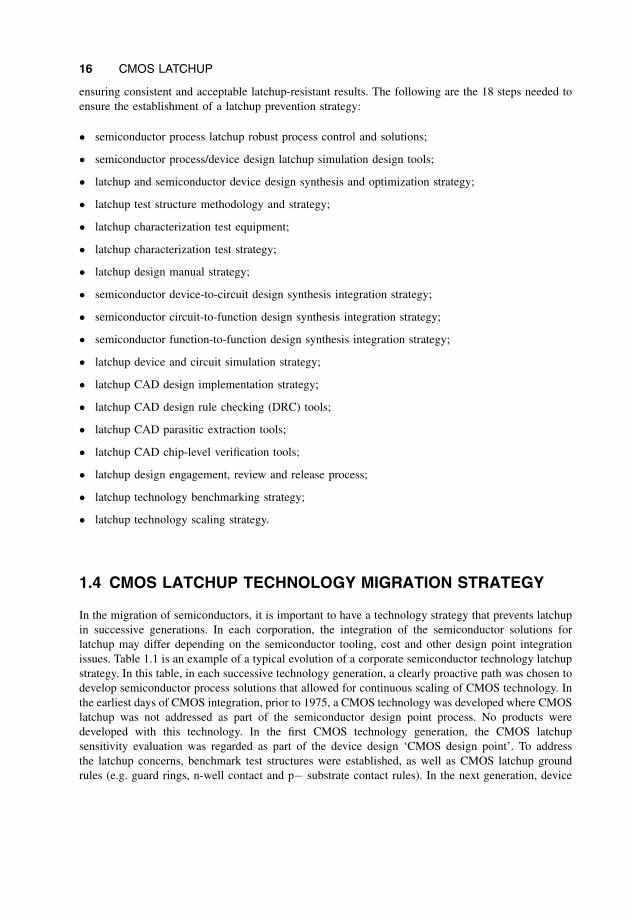
wafer resistance is scaled to higher substrate doping concentrations. Figure 1.5 shows the scaling of the
substrate resistance with time, as a function of application frequency. Figure 1.5 shows that with scaling
the direction is toward higher substrate resistance. Substrate resistance will strongly influence the CMOS
latchup robustness. First, the substrate resistance is critical in the shunt substrate resistance (which will be
discussed in the following sections). Second, low doping concentration leads to long minority carrier
lifetimes. Finally, the ability to dissipate local and global self-heating becomes an increasing concern.
One of the key issues in CMOS latchup scaling is that the lateral scaling occurs at a much faster rate than
the vertical scaling. As a result, the scalings of the isolation, n-well, p-well and epitaxial regions are not
synchronous with lateral scaling issues. Hence, the geometric similitude is violated in the two-dimensional
cross section, leading to difficulty in the production of a scalable ‘model’. Hence, one of the issues associated
withCMOSlatchup is the n-well andp-well design,whichwill be discussed indetail in the following sections.
To abide by MOSFET constant electric field scaling theory, the power supply voltage is reduced with
technology scaling. The scaling of the power supply voltage allows key CMOS latchup metrics to have
CMOS latchup conditions above the power supply voltage (e.g. holding voltage). In the case where the
latchup injection and voltage sources are also scaling, there is no concern. But, in the case where the latchup
source event is not scaling (e.g. cable discharge events (CDEs) and ionizing radiation), this can be an issue.
One of the key issues is the CMOS latchup holding voltage VH. The holding voltage is the voltage at
the low-voltage/high-current state that occurs during latchup. A concern is the relative value of the
holding voltage versus the power supply voltage. As a technology is scaled, the holding voltage
decreases. Table 1.2 show an example of the trend of VH and pþ/nþ space as a function of technology
resistance (Ω cm)
Figure 1.5 Scaling of substrate wafer resistivity as a function of time and application frequency.
Table 1.2 Holding voltage and pþ/nþ space as a function of technology generation.
Technology generation(mm) pþ/nþ space(mm) Holding voltage (V)
0.5 2.0 6
0.35 1.6 5.5
0.22 1.3 3.7
0.18 1.0 2.7
0.13 0.8 2.7
20 CMOS LATCHUP
generation. In each generation, the power supply voltage is also lowered. As a result, VH and VDD are
scaling with semiconductor device size reduction.
1.7 KEY DEVELOPMENTS
There are key developments that influenced the directions and solutions of semiconductor technology
and the art of the latchup discipline. In this section, a brief list of key innovations, contributions,
technical works and patents that influenced the direction of latchup is shown.
1.7.1 Key Innovations
Key innovations that significantly influenced latchup are primarily those associated with semiconductor
evolution and layout design directions. The semiconductor technology features that highly influenced
CMOS and BiCMOS latchup robustness are as follows:
introduction of the implanted MeV retrograde well;
introduction of STI;
introduction of pþþ substrates;
introduction of pþþ buried layers;
introduction of DT isolation;
introduction of subcollector implants.
The innovations that have had the greatest influence on the semiconductor design are the following:
introduction of single and dual guard ring structures;
introduction of n-well and substrate contact resistance design rules and verification systems;
introduction of the JEDEC latchup specification and commercial qualification of semiconductor
components.
1.7.2 Key Contributions
In the latchup field, accomplishments to advance the field are in the form of development of experimental
discovery, analytical models, introduction of new semiconductor devices and circuits, test equipment and
test methods. Below is a short chronological list of key events that influenced the field of latchup:
1967: Poll and Leavy demonstrated ‘transient radiation induced CMOS latchup’ [8, 9]. This work
demonstrated that ‘single event latchup’ and other radiation environments can induce CMOS
latchup in space applications.
1973: Shafer and Gregory addressed commercial application usage of CMOS and CMOS latchup
implications [12–14].
1976: Dawes and Derbenwick demonstrated CMOS latchup improvements with gold doping [28].
KEY DEVELOPMENTS 21
1978: Estreich et al. demonstrated latchup improvements using epitaxial buried layer process
[29–33].
1979: Adams and Sokel demonstrated usage of neutron irradiation to control CMOS latchup [27].
This work showed that nuclear irradiation modifies the parasitic bipolar current gains.
1980: Estreich’s thesis ‘The physics and modeling of latch-up in CMOS integrated circuits’
provided significant advancement on latchup theory [33]. This work significantly advanced
analytical models, characterization and latchup characterization structures of CMOS.
1982: Parillo demonstrated ‘dual-well CMOS’ advantages for CMOS latchup. The significance of this
work is the demonstration of the CMOS latchup advantages of an n-well and a p-well region [39].
1983: Takacs et al. demonstrated CMOS latchup in CMOS structures with and without epitaxy in a
field oxide (FOX) technology [56]. This work demonstrated that a two order of magnitude
improvement is achievable in the CMOS latchup critical current with epitaxial layers as well as
demonstrated that CMOS latchup critical voltage is surface induced due to field oxide scaling.
1982: Rung et al. demonstrated usage of deep trench isolation for CMOS technology. This work
demonstrated the advantage of deep trench structures for isolation of CMOS p-channel and
n-channel MOSFET devices [47]. Today, this work is significant for BiCMOS and smart power
applications.
1983: Troutman demonstrated the improvement in guard ring efficiency utilizing p epitaxial/pþþsubstrate wafers [59].
1983: Troutman and Zappe developed theory for transient latchup [49, 50]. From Zappe’s thesis,
significant progress was made in the understanding of transient latchup analysis.
1982: Troutman developed an automated latchup test system that varies substrate and well
resistances for the quantification of CMOS latchup design space as a function of well and
substrate resistances. This work established a design methodology for CMOS latchup design
point analysis.
1983: Troutman developed the generalized differential tetrode criterion for CMOS latchup. This work
provided a better analytical relationship for the ‘beta product’ and ‘alpha sum’ latchup criteria [79].
1984: Troutman integrated the retrograde well into IBM’s CMOS IV technology for a 0.8-mm CMOS
DRAM and logic technology generation. The significance of this work was the first commercial
integration of an MeV retrograde well implanter into a commercial CMOS technology.
1984: Terrill and Hu developed a substrate resistance model for CMOS latchup modeling. The
significance of the work is that the model addresses spreading resistance in the substrate [71].
1985: Troutman wrote the first textbook on CMOS latchup, ‘CMOS Latchup: The Problem and the
Cure’ [79].
1985: Hargrove and Troutman developed a substrate transmission line model for CMOS latchup
[62]. This work was the initial step in providing a better substrate model for the understanding of
CMOS latchup in a p epitaxial/pþþ wafer.
1986: Voldman demonstrated retrograde well–substrate modulation leading to variations in the
CMOS latchup sensitivity in a 4-MB DRAM 0.8-mm technology [80]. This work demonstrated the
need for cosynthesis of epitaxy thickness control, retrograde well energy and dose module in a
p epitaxial/pþþ heavily doped wafer [80–82].
22 CMOS LATCHUP
1986: Chern and Wu developed a new analytical three-dimensional model for substrate resistance in
CMOS latchup structures. The significance of this work is that it addresses the substrate spreading
resistance associated with majority carrier current during latchup events.
1991: Johnston et al. addressed the effect of temperature on single-particle latchup (e.g. SEL). The
significance is experimental verification of the temperature dependence relationship of the latchup
capture cross section and the linear energy transfer (LET) threshold [155]. This is critical to the
evaluation of SEL in space and terrestrial applications.
1992: Voldman demonstrated the issue of retrograde well–substrate modulation on both ESD and
CMOS latchup in a 0.5-mm technology. The first significance of the work was the cooptimization of
CMOS latchup and ESD networks. The second significant issue was the impact of the MeV
retrograde well implant energy and dose on CMOS latchup scaling and ESD scaling for scaled
CMOS technology. Finally, this work demonstrated how to develop semiconductor processes that
can achieve ESD robust diode networks and improved CMOS latchup in each technology
generation; this work influenced the commercial usage of MeV high-energy implanters for
advanced CMOS technology and future CMOS scaling [81–86].
1992: Borland proposed the ‘buried implant layer and lateral isolation’ (BILLI) semiconductor
process for the utilization of a blanket implant and LOCOS isolation technology. The significance
of the work is the utilization of buried layers for latchup improvement. This concept did not
integrate into the mainstream CMOS technology, instead chose the path of heavily doped retrograde
n-wells and p-wells, as well as triple well.
1993: SEMATECH established a ‘vertical modulated well (VMW)’ research effort on the
integration of retrograde well with scaled CMOS. During this time frame, only one corporation
was using retrograde well in standard offerings, and all other US corporations used diffused well
CMOS. This accelerated the integration of retrograde wells in many corporations today.
1993: Morris (at SEMATECH) focused on the utilization of heavily doped buried layers for
future scaled CMOS. This work demonstrated the value of HDBL for latchup in scaled CMOS
technology.
1995: Bafluer et al. addressed latchup concerns in smart power technology [172]. The significance
was highlighting the reverse-current problem and LDMOS devices’ latchup-related issues.
1996: Barak et al. addressed the relationship of single event upset (SEU) and SEL. This work
highlighted the interaction between circuit soft error rate, system disturbances and single event
latchup, as well as addressed global chip interactions [171].
1998: Li’s thesis ‘Design automation for reliable CMOS chip I/O circuits’ demonstrated advance-
ment in CAD concepts related to latchup [88–90]. This work (a) implemented Troutman’s transfer
resistance representation of the substrate to a full CAD tool implementation and (b) extracted
parasitic pnp or npn bipolar elements that are extracted, identified and added to its supported device
representation (e.g. associated with the parasitic transistor) [88–90].
2000: Winkler and Herzl focused on ‘active guard ring’ concepts for noise suppression in mixed
signal chip using on-chip driven guard rings. These concepts are presently being applied to smart
power applications for BCD technology [176].
2002: Vashenko and Concannon demonstrated the relationship between injection current magnitude
and distance between the injection source and the CMOS circuit. This work highlighted the
domains of CMOS latchup failure. This work is unpublished.
KEY DEVELOPMENTS 23

2002: Rubin and Morris integrated heavily doped buried layers into technologies to demonstrate
CMOS latchup advantages versus technology trade-offs [91]. This work showed the CMOS latchup
improvement with the lower substrate shunt resistance in a p substrate wafer.
2000: Parthasarathy et al. addressed the usage of deep trench for isolation in HVCMOS [181].
2003: Morris demonstrated CMOS scaling implications for future CMOS technologies [92]. The
significance of the work is the demonstration that CMOS latchup is predicted to be an issue in the
future, and new process solutions will be needed in the future.
2002: Voldman developed the concept of integration of the ‘transmission line pulse’ test
methodology with the picocurrent analysis (PICA) tool for visualization of CMOS latchup
propagation in space and time. This tool concept was first experimentally performed by the IBM
T. J. Watson team of Weger and Sanda [94]. This work demonstrated the ability to determine the
time delay between the injection phenomenon and the CMOS latchup event.
2003: Stellari demonstrated CMOS latchup propagation using CCD methodology [95]. This work
similarly to the work of Weger et al. showed the propagation of CMOS latchup within a dense
CMOS logic region.
2003: Boselli et al. evaluated through simulation the CMOS scaling in a 65-nm technology node
[93].
2003: Horn’s PhD thesis ‘On the reverse-current problem in integrated smart power circuits’
analyzed the effectiveness of ‘compensating active guard ring’ techniques for smart power circuits
[185].
2003: ESD Association released the Transient Latchup (TLU) standard practice (SP) document
ESD DSP5.4-2003 on power supply transient stimulation events. Key contributors included I.
Morgan (AMD), G. Weiss (AT&T) and C. O’Connor (UTI). The significance of the work was to
address power supply transients for both positive and negative events on power supply rails.
2004: Watson and Voldman evaluated the CMOS latchup characteristics of a BiCMOS silicon
germanium DT structure. The study extended the work of Rung et al. by evaluating deep trench and
a subcollector for CMOS latchup improvements. This work demonstrated that the subcollector leads
to significant improvements when added to the deep trench; this has significant implications for
CMOS latchup robustness improvement for automotive and space applications [98–101].
2005: Voldman demonstrated the implications of ‘merged triple-well’ technology. This work demon-
strated that the merged triple-well implementation leads to undershoot CMOS latchup robustness
degradation and overshoot CMOS robustness enhancement [104,105].
2005: Voldman demonstrated the advantage of a ‘trench isolation’ technology utilized for a low-cost
BiCMOS silicon germanium technology [103]. The significance of this work is the evaluation of a
second trench concept – a new low-cost trench technology integrated with implanted subcollectors
demonstrating CMOS latchup robustness well above 0.22-, 0.18- and 0.13-mm CMOS technologies
on low-doped substrate wafers [103].
2005: Huh et al. demonstrated CMOS latchup issues associated with SOC integration (power supply
to power supply and I/O to I/O latchup events). This work has significant implications on CMOS
design integration and CAD methodologies [108].
2005: Voldman further developed analytical development of CMOS latchup domino theory. A
significant result is the extension of the theory of the differential generalized latchup criterion
24 CMOS LATCHUP
(developed by Troutman) including the external injection source. This criterion can be applied for
external latchup processes [97].
2005: Voldman demonstrated CMOS latchup in ultrahigh resistive wafers of 1–5 k cm CMOS
substrates. This work demonstrated that the p-well region has a significant influence on the CMOS
latchup; this work demonstrated that ultrahigh resistivity wafers will be suitable in the future for RF
CMOS, RF BiCMOS, RF BiCMOS silicon germanium, and other SOC and NOC applications that
require high performance and low noise [106].
2005: Zhan and Wang provided a ‘model graph’ representation of the extraction of a parasitic pnpn.
The significance of the work was utilization of model graph representation applied to CMOS
latchup extraction, checking and verification CAD tool development [109, 110].
2006: ESD Association Work Group 14 (WG14) released system-level CDE measurement standard
practice document. The significance of this work is associated with the growing problem of
CMOS latchup events due to cable discharge in systems, boards and chips in advanced CMOS
technologies.
1.7.3 Key Patents
CMOS latchup was a concern in CMOS technology, as the interest increased for commercial
applications. As a result, there were a significant number of patents to address the semiconductor
process, circuit and CAD solutions. In the early 1980s, CMOS latchup focus was on circuit solutions
and semiconductor processes that integrated latchup solutions with single-well CMOS technology.
Early patents addressed CMOS isolation methods and the integration of guard rings with CMOS
technology for CMOS latchup. This was followed by dual-well CMOS technology patents. In this time
frame, high-energy implanters were developed, leading to a focus on retrograde well implantation as
well as high-energy MeV implantation buried layers. In the 1980s, focus also began on circuit solutions
for CMOS latchup. In the 1990s and more recently in 2000, the focus has been on CAD tools for
extraction, checking and verification, new process features, novel processes and novel failure analysis
techniques. With CMOS scaling, patents have focused on quantifying CMOS latchup and design
integration into high-density CMOS technology. Additionally, the cosynthesis of CMOS scaling, noise
and latchup for RF applications and SOC environments has led to an interest in BiCMOS solutions
from process, circuit and integration perspectives for improved CMOS latchup robustness.
1.8 LATCHUP FAILURE MECHANISMS
Latchup failure mechanisms can occur on both a local and a global level in chip, board and system
environments. Table 1.3 contains failure mechanisms observed in CMOS latchup events. For latchup
events that occur in a signal pad, the failure mechanism is typically observed in CMOS inverter
circuits. In CMOS inverter circuits, latchup is observed in the parasitic pnpn formed between the p- and
the n-channel MOSFET. The failures typically occur near the insulators and metallurgical junction
regions. These failures are evident for contact, silicide and metallurgical junction failures.
At the power pads, typically latchup is evident from a signature of metallization failure of VDD and
VSS power rails. Power rail failure of the metallurgy can also occur from HBM (human body model),
MM (machine model) and CDM (charged device model) events; in the case of latchup, there is most
likely evidence of logic circuitry failure.
LATCHUP FAILURE MECHANISMS 25
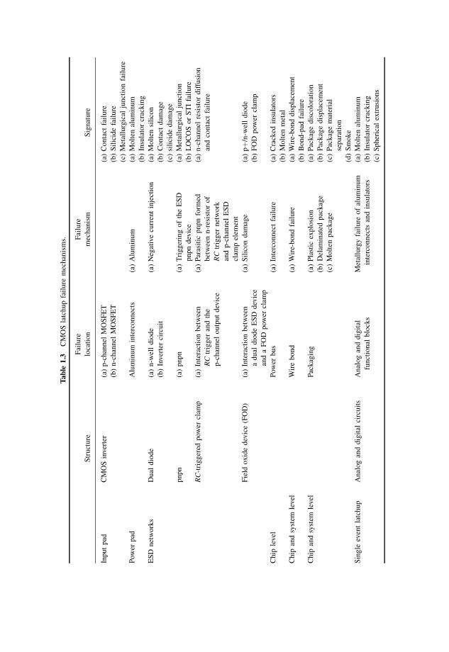
Table
1.3
CMOSlatchupfailure
mechanisms.
Failure
Failure
Structure
location
mechanism
Signature
Inputpad
CMOSinverter
(a)p-channel
MOSFET
(b)n-channel
MOSFET
(a)Contact
failure
(b)Silicidefailure
(c)Metallurgical
junctionfailure
Power
pad
Aluminum
interconnects
(a)Aluminum
(a)Molten
aluminum
(b)Insulatorcracking
ESD
networks
Dual
diode
(a)n-w
elldiode
(b)Invertercircuit
(a)Negativecurrentinjection
(a)Molten
silicon
(b)Contact
dam
age
(c)silicidedam
age
pnpn
(a)pnpn
(a)TriggeringoftheESD
pnpndevice
(a)Metallurgical
junction
(b)LOCOSorSTIfailure
RC-triggered
power
clam
p(a)Interactionbetween
RCtrigger
andthe
p-channel
outputdevice
(a)Parasitic
pnpnform
ed
betweenn-resistorof
RCtrigger
network
andp-channel
ESD
clam
pelem
ent
(a)n-channel
resistordiffusion
andcontact
failure
Field
oxidedevice(FOD)
(a)Interactionbetween
adual
diodeESD
device
andaFOD
power
clam
p
(a)Silicondam
age
(a)pþ/n-w
elldiode
(b)FOD
power
clam
p
Chip
level
Power
bus
(a)Interconnectfailure
(a)Cracked
insulators
(b)Molten
metal
Chip
andsystem
level
Wirebond
(a)Wire-bondfailure
(a)Wire-bonddisplacement
(b)Bond-pad
failure
Chip
andsystem
level
Packaging
(a)Plastic
explosion
(b)Delam
inated
package
(c)Molten
package
(a)Packagediscoloration
(b)Packagedisplacement
(c)Packagematerial
separation
(d)Smoke
Single
eventlatchup
Analoganddigital
circuits
Analoganddigital
functional
blocks
Metallurgyfailure
ofaluminum
interconnectsandinsulators
(a)Molten
aluminum
(b)Insulatorcracking
(c)Spherical
extrusions
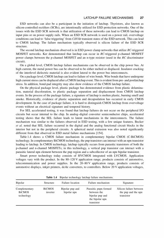
ESD networks can also be a participant in the initiation of latchup. Thyristors, also known as
silicon-controlled rectifiers (SCRs), are intentionally utilized for ESD protection networks. One of the
issues with the ESD SCR network is that utilization of these networks can lead to CMOS latchup on
input pins or on power supply rails. When an ESD SCR network is used on a power rail, overvoltage
conditions can lead to ‘false triggering’ from CdV/dt transient states of the ESD network. This can lead
to CMOS latchup. The failure mechanism typically observed is silicon failure of the ESD SCR
structure.
The second latchup mechanism observed is in ESD power clamp networks that utilize RC-triggered
MOSFET networks. Ker demonstrated that latchup can occur in RC-triggered p-channel MOSFET
power clamps between the p-channel MOSFET and an n-type resistor (used in the RC discriminator
circuit).
On a global level, CMOS latchup failure mechanisms can be observed in the chip power bus. At
high current, the metal power bus can be observed to be either melted or displaced. Insulator cracking
of the interlevel dielectric material is also evident lateral to the power bus interconnects.
On a package level, CMOS latchup can lead to failure of wire bonds. Wire bonds that have undergone
high current stress can be displaced after a CMOS latchup event. This is evident from pre- and postlatchup
stress. In addition, bond-pad integrity may also show evidence of the CMOS latchup failure.
On the physical package level, plastic package has demonstrated evidence from plastic delamina-
tion, material discoloration, to plastic package separation and displacement from CMOS latchup
events. In the process of the package failure, a signature of latchup is molten plastic, burning smell and
smoke. Historically, evidence of plastic separation and decapsulation has occurred in early CMOS
development. In the case of package failure, it is hard to distinguish CMOS latchup from overvoltage
events without an electrical signature and temporal history.
For SEL accelerated testing, it was found that latchup failures do not occur on the peripheral I/O
circuits but occur internal to the chip. In analog–digital converter semiconductor chips, accelerated
testing shows that the SEL failure leads to latent mechanisms in the interconnects. The failure
mechanism was similar to the failures observed in ESD testing, with a few unique features. Becker
et al. noted that SEL failure occurred in the digital and the analog functional circuit blocks in the
interior but not in the peripheral circuits. A spherical metal extrusion was also noted significantly
different from that observed in ESD metal failure mechanisms [154].
Table 1.4 shows a CMOS failure mechanism in complementary bipolar CMOS (C-BiCMOS)
technology. In complementary BiCMOS technology, the pnp transistor can interact with an npn transistor
leading to latchup. In CMOS technology, latchup typically occurs from parasitic transistors of both the
p-channel and n-channel MOSFETs; in this technology, a vertical pnp transistor can interact with a
parasitic lateral npn element between the pnp region and a subcollector of an npn bipolar transistor.
Smart power technology today consists of HVCMOS integrated with LVCMOS. Application
voltages vary with the product. In the 80–120 V application range, products consists of automotive,
telecommunication and power supplies. In the 20–80 V application range, products consists of
automotive displays, inkjet printers, dc/dc converters, to controllers. Below 20 V application voltages,
Table 1.4 Bipolar technology latchup failure mechanisms.
Bipolar Structure Failure location Failure mechanism Signature
Complementary
BiCMOS
technology
BiCMOS
inverter
Bipolar pnp and
bipolar npn
Parasitic pnpn formed
between the
bipolar pnp and
the bipolar npn
transistor
Silicon failure between
the pnp and the npn
transistor
LATCHUP FAILURE MECHANISMS 27
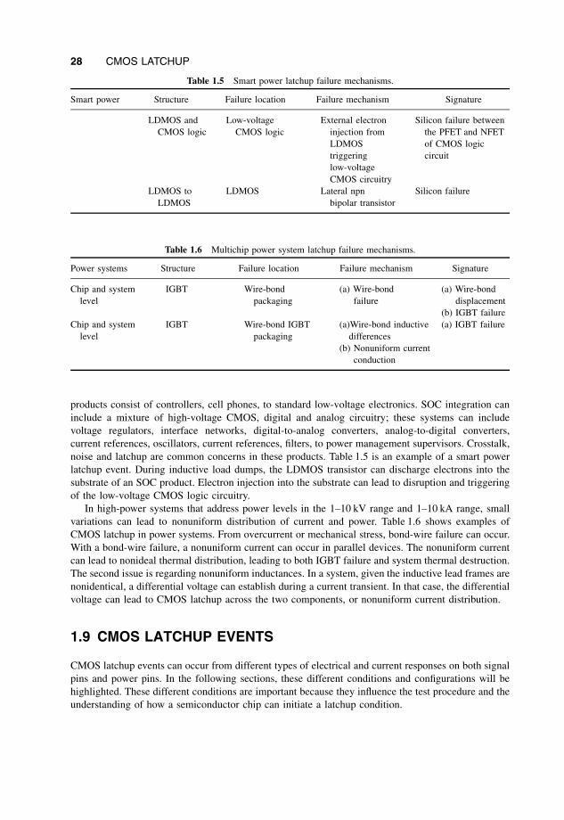
products consist of controllers, cell phones, to standard low-voltage electronics. SOC integration can
include a mixture of high-voltage CMOS, digital and analog circuitry; these systems can include
voltage regulators, interface networks, digital-to-analog converters, analog-to-digital converters,
current references, oscillators, current references, filters, to power management supervisors. Crosstalk,
noise and latchup are common concerns in these products. Table 1.5 is an example of a smart power
latchup event. During inductive load dumps, the LDMOS transistor can discharge electrons into the
substrate of an SOC product. Electron injection into the substrate can lead to disruption and triggering
of the low-voltage CMOS logic circuitry.
In high-power systems that address power levels in the 1–10 kV range and 1–10 kA range, small
variations can lead to nonuniform distribution of current and power. Table 1.6 shows examples of
CMOS latchup in power systems. From overcurrent or mechanical stress, bond-wire failure can occur.
With a bond-wire failure, a nonuniform current can occur in parallel devices. The nonuniform current
can lead to nonideal thermal distribution, leading to both IGBT failure and system thermal destruction.
The second issue is regarding nonuniform inductances. In a system, given the inductive lead frames are
nonidentical, a differential voltage can establish during a current transient. In that case, the differential
voltage can lead to CMOS latchup across the two components, or nonuniform current distribution.
1.9 CMOS LATCHUP EVENTS
CMOS latchup events can occur from different types of electrical and current responses on both signal
pins and power pins. In the following sections, these different conditions and configurations will be
highlighted. These different conditions are important because they influence the test procedure and the
understanding of how a semiconductor chip can initiate a latchup condition.
Table 1.5 Smart power latchup failure mechanisms.
Smart power Structure Failure location Failure mechanism Signature
LDMOS and
CMOS logic
Low-voltage
CMOS logic
External electron
injection from
LDMOS
triggering
low-voltage
CMOS circuitry
Silicon failure between
the PFET and NFET
of CMOS logic
circuit
LDMOS to
LDMOS
LDMOS Lateral npn
bipolar transistor
Silicon failure
Table 1.6 Multichip power system latchup failure mechanisms.
Power systems Structure Failure location Failure mechanism Signature
Chip and system
level
IGBT Wire-bond
packaging
(a) Wire-bond
failure
(a) Wire-bond
displacement
(b) IGBT failure
Chip and system
level
IGBT Wire-bond IGBT
packaging
(a)Wire-bond inductive
differences
(b) Nonuniform current
conduction
(a) IGBT failure
28 CMOS LATCHUP
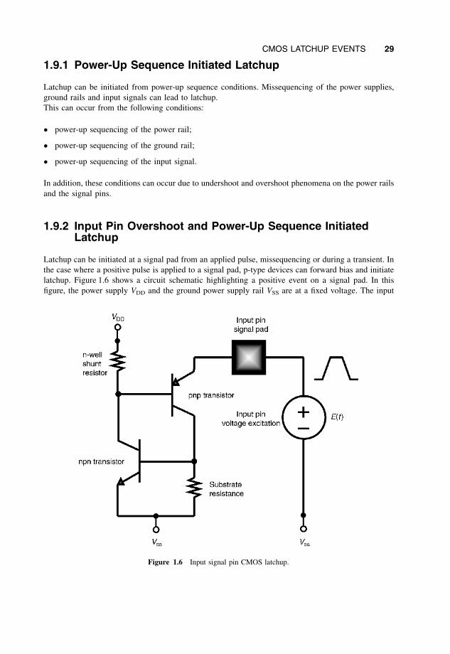
1.9.1 Power-Up Sequence Initiated Latchup
Latchup can be initiated from power-up sequence conditions. Missequencing of the power supplies,
ground rails and input signals can lead to latchup.
This can occur from the following conditions:
power-up sequencing of the power rail;
power-up sequencing of the ground rail;
power-up sequencing of the input signal.
In addition, these conditions can occur due to undershoot and overshoot phenomena on the power rails
and the signal pins.
1.9.2 Input Pin Overshoot and Power-Up Sequence InitiatedLatchup
Latchup can be initiated at a signal pad from an applied pulse, missequencing or during a transient. In
the case where a positive pulse is applied to a signal pad, p-type devices can forward bias and initiate
latchup. Figure 1.6 shows a circuit schematic highlighting a positive event on a signal pad. In this
figure, the power supply VDD and the ground power supply rail VSS are at a fixed voltage. The input
Figure 1.6 Input signal pin CMOS latchup.
CMOS LATCHUP EVENTS 29
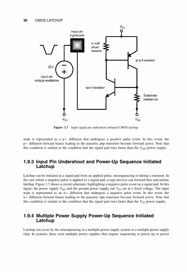
node is represented as a pþ diffusion that undergoes a positive pulse event. In this event, the
pþ diffusion forward biases leading to the parasitic pnp transistor become forward active. Note that
this condition is similar to the condition that the signal pad rises faster than the VDD power supply.
1.9.3 Input Pin Undershoot and Power-Up Sequence InitiatedLatchup
Latchup can be initiated at a signal pad from an applied pulse, missequencing or during a transient. In
the case where a negative pulse is applied to a signal pad, n-type devices can forward bias and initiate
latchup. Figure 1.7 shows a circuit schematic highlighting a negative pulse event on a signal pad. In this
figure, the power supply VDD and the ground power supply rail VSS are at a fixed voltage. The input
node is represented as an nþ diffusion that undergoes a negative pulse event. In this event, the
nþ diffusion forward biases leading to the parasitic npn transistor become forward active. Note that
this condition is similar to the condition that the signal pad rises faster than the VSS power supply.
1.9.4 Multiple Power Supply Power-Up Sequence InitiatedLatchup
Latchup can occur by the missequencing in a multiple power supply system or a multiple power supply
chip. In systems, there exist multiple power supplies that require sequencing to power up or power
Figure 1.7 Input signal pin undershoot initiated CMOS latchup.
30 CMOS LATCHUP
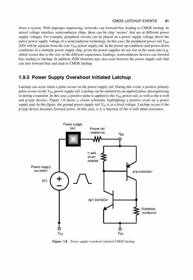
down a system. With improper sequencing, networks can forward bias leading to CMOS latchup. In
mixed voltage interface semiconductor chips, there can be chip ‘sectors’ that are at different power
supply voltages. For example, peripheral circuits can be placed on a power supply voltage above the
native power supply voltage of a semiconductor technology. In this case, the peripheral power rail VDD
(I/O) will be separate from the core VDD power supply rail. In the power-up condition (and power-down
condition) of a multiple power supply chip, given the power supplies do not rise at the same rate (e.g.
which occurs due to the size of the different capacitance loading), semiconductor devices can forward
bias leading to latchup. In addition, ESD elements may also exist between the power supply rails that
can also forward bias and lead to CMOS latchup.
1.9.5 Power Supply Overshoot Initiated Latchup
Latchup can occur when a pulse occurs on the power supply rail. During this event, a positive polarity
pulse occurs on the VDD power supply rail. Latchup can be initiated by an applied pulse, missequencing
or during a transient. In this case, a positive pulse is applied to the VDD power rail, as well as the n-well
and p-type devices. Figure 1.8 shows a circuit schematic highlighting a positive event on a power
supply pad. In this figure, the ground power supply rail VSS is at a fixed voltage. Latchup occurs if the
p-type device becomes forward active. In this case, it is a function of the n-well shunt resistance.
Figure 1.8 Power supply overshoot initiated CMOS latchup.
CMOS LATCHUP EVENTS 31

1.9.6 Power Supply Undershoot Initiated Latchup
Latchup can occur when a negative pulse occurs on the power supply rail. During this event, a negative
polarity pulse occurs on the VDD power supply rail. Latchup can be initiated by an applied pulse or an
oscillating signal. In the case where a negative pulse is applied to the VDD power rail, when the VDD
power rail goes below the VSS power supply rail, the n-well forward biases leading to injection into the
substrate. Figure 1.9 shows a circuit schematic highlighting a negative event on a power supply pad. In
this figure, the ground power supply rail VSS is at a fixed voltage. Latchup occurs if the negative signal
is followed by a positive rising signal leading to the p-type device become forward active.
1.9.7 Power Supply (Ground Rail) Undershoot Initiated Latchup
Latchup can occur when a pulse occurs on the ground power supply rail. During this event, a negative
polarity pulse occurs on the VSS power supply rail. Latchup can be initiated by an applied pulse,
missequencing or during a transient. In this case, a negative pulse is applied to the VSS power rail, as
well as the p substrate and n-type devices. Figure 1.10 shows a circuit schematic highlighting a
negative event. In this figure, the power supply rail VDD is at a fixed voltage. Latchup occurs if the
n-type device becomes forward active. In this case, it is a function of the p substrate shunt resistance.
Figure 1.9 Power supply undershoot initiated CMOS latchup.
32 CMOS LATCHUP
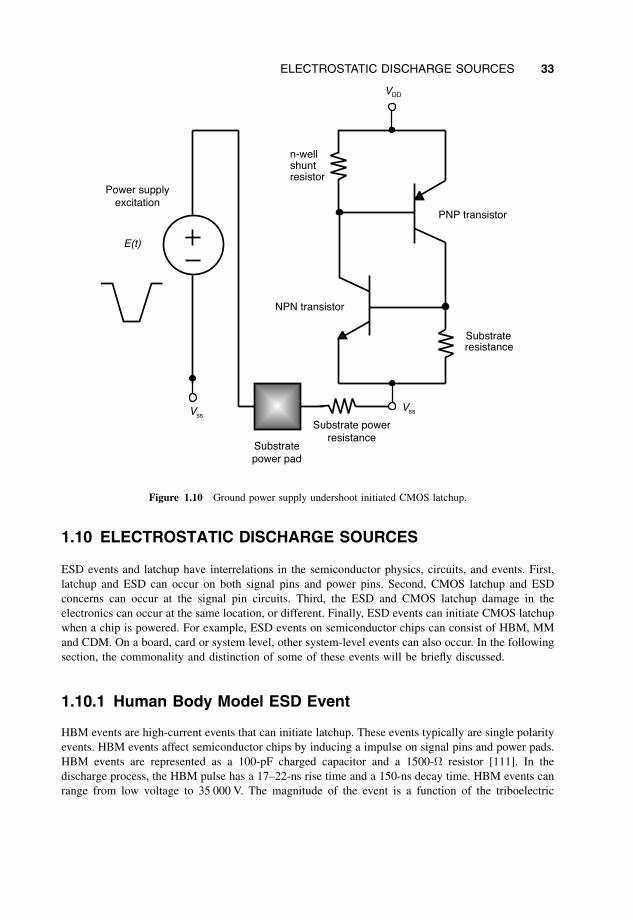
1.10 ELECTROSTATIC DISCHARGE SOURCES
ESD events and latchup have interrelations in the semiconductor physics, circuits, and events. First,
latchup and ESD can occur on both signal pins and power pins. Second, CMOS latchup and ESD
concerns can occur at the signal pin circuits. Third, the ESD and CMOS latchup damage in the
electronics can occur at the same location, or different. Finally, ESD events can initiate CMOS latchup
when a chip is powered. For example, ESD events on semiconductor chips can consist of HBM, MM
and CDM. On a board, card or system level, other system-level events can also occur. In the following
section, the commonality and distinction of some of these events will be briefly discussed.
1.10.1 Human Body Model ESD Event
HBM events are high-current events that can initiate latchup. These events typically are single polarity
events. HBM events affect semiconductor chips by inducing a impulse on signal pins and power pads.
HBM events are represented as a 100-pF charged capacitor and a 1500- resistor [111]. In the
discharge process, the HBM pulse has a 17–22-ns rise time and a 150-ns decay time. HBM events can
range from low voltage to 35 000 V. The magnitude of the event is a function of the triboelectric
VssVss
VDD
n-well shunt resistor
PNP transistor
NPN transistor
E(t)
resistance
Substrate powerresistance
Power supplyexcitation
Substratepower pad
Substrate
Figure 1.10 Ground power supply undershoot initiated CMOS latchup.
ELECTROSTATIC DISCHARGE SOURCES 33
charging, the charging process and the humidity. There are a few reasons why HBM events do not
cause CMOS latchup:
HBM events occur when the semiconductor chip is unpowered.
HBM events’ total charge is small (small capacitance and short time event).
But what if the chip was powered when an HBM was applied?
How does one distinguish damage from an HBM event from CMOS latchup?
Damage patterns of HBM events are restricted typically to peripheral circuits, ESD networks and
interconnect wiring (input wires and bussing).
HBM time response is a faster event; hence, the material motion (e.g. electromigration) is typically
not observed.
Damage patterns of latchup events can involve semiconductor devices, circuits, bussing and
packaging. Typical HBM events do not demonstrate package damage.
1.10.2 Machine Model ESD Event
MM events are high-current events that can initiate latchup. Machine models are oscillatory polarity
events that are more likely to induce latchup events [112]. MM events are represented as a 200-pF
charged capacitor and no resistor. In the discharge process, the rise time is faster than that for an HBM
event. There are a few reasons why MM events do not typically cause CMOS latchup:
MM events occur when the semiconductor chip is unpowered.
Although MM events are not typically observed, they do induce an oscillating transient that can lead to
latchup given a system was powered. When the signal pad or power pad undergoes a negative transient,
electrons can be discharged into the substrate potentially initiating the npn parasitic devices. With the
positive polarity transition, the pnp transistor is also initiated. The primary reason that this is not a
concern is these events occur during an unpowered chip state. But, what if the chip or system is
powered? How does one distinguish damage from an MM event from latchup?
Damage patterns of MM events are restricted typically to peripheral circuits, ESD networks and
interconnect wiring (input wires and bussing).
MM events are faster events, and hence do not involve significant material motion (e.g. electro-
migration).
Damage patterns of latchup events can involve semiconductor devices, circuits, bussing and
packaging. Typical MM events do not demonstrate package damage.
1.10.3 Cable Discharge Event Source
CDE is a growing source of latchup events that occur on a card or system level [113–127]. Electrical
discharge from charged cables has been a concern in electrical systems. An electrical cable behaves as
34 CMOS LATCHUP

a transmission line having both capacitive and inductive characteristics. The charge stored in an
electrical cable can be evaluated according to the stored capacitance per unit length. As the length of
the cable increases, the amount of stored charge in the cable increases. In an ‘unsocketed’ cable, the
charge is stored between the center and outer conductors across the insulator region. When the voltage
across the insulator exceeds the insulator breakdown voltage, an electrical discharge occurs between
the outer and inner conductors. In the case where the voltage remains below the breakdown voltage, the
stored charge remains in the cable, leaving the cable as a charged cable. When the charged cable center
conductor approaches a system, an electrical arc occurs between the center conductor and the electrical
system input signals. With the cable discharge event to the system-level inputs, a significant current can
discharge to the signal pin leading to latchup in the semiconductor chips integrated into the system
components. Given a system that is unpowered, no latchup event can occur. But if the CDE occurs
while a system is powered, the current event can lead to CMOS latchup. With the integration of wide
area network (WAN) and local area network (LAN), the Ethernet is playing a larger role. When a
charged twisted pair cable connects to an Ethernet port with a lower electrical potential, CDE can occur
in LAN systems. Figure 1.11 shows an example of a typical CDE waveform. In the past, standards (e.g.
IEEE 802.3 Section 14.7.2) have noted the potential for CDE processes in LAN cables. As the number
of electronic circuits increases, the number of I/O ports also increases (e.g. Rent’s Rule). As the number
of I/O ports increases, there is an increase in the number of electrical cable connections. As a result,
future systems have an increasing number of electrical cable connections. This increases the likelihood
of a charged cable connection leading to CMOS latchup. Hence, with both system and technology
evolution, the reasons for the increased concern for this issue are the following:
WAN and LAN integration;
category 5 and 6 LAN cabling;
higher level incidents of disconnection;
high level incidents of reconnections;
width
overshoot
Figure 1.11 CDE waveform.
ELECTROSTATIC DISCHARGE SOURCES 35
CMOS technology migration to p substrates;
CMOS technology scaling of pþ/nþ scaling;
CMOS technology scaling of shallow trench isolation;
competitive focus on cost reduction and the elimination of future latchup solutions.
The primary reasons that CDEs are a latchup concern are as follows:
The systems that are experiencing cable discharge events are powered systems where the cable is
inserted.
The total charge and current magnitude from many cable discharge events exceed the CMOS
latchup design specification (e.g. JEDEC specification).
The CDEs are occurring on high data rate transfer ports that have interface circuits consisting of
advanced CMOS technology with low CMOS latchup robustness.
1.11 SINGLE EVENT LATCHUP
SEL is an event where a single-particle interaction with a semiconductor chip or system can lead to
latchup and destruction of the data transfer, semiconductor chip or system failure [128–171]. SEL can
be initiated by a wide range of particle types and events. SEL can be initiated by the following set of
particles:
high-energy photons;
alpha particles;
cosmic rays;
heavy ions.
The primary reasons why CMOS latchup is a concern in space applications are the following:
wide spectrum of particle types (e.g. neutrons, protons and muons);
wide energy spectrum and environments (e.g. space and terrestrial);
single event source does not scale with technology generation (e.g. nonscalable source);
destructive nature of CMOS latchup events (e.g. device damage and system-level damage);
inability to repair or introduce redundant functions in space applications;
cost of the space application.
1.11.1 High-Energy Photon Emissions
High-energy photons can lead to photocurrent generation in a metallurgical junction. The two
processes of the current collection at a metallurgical junction are associated with photogeneration
36 CMOS LATCHUP
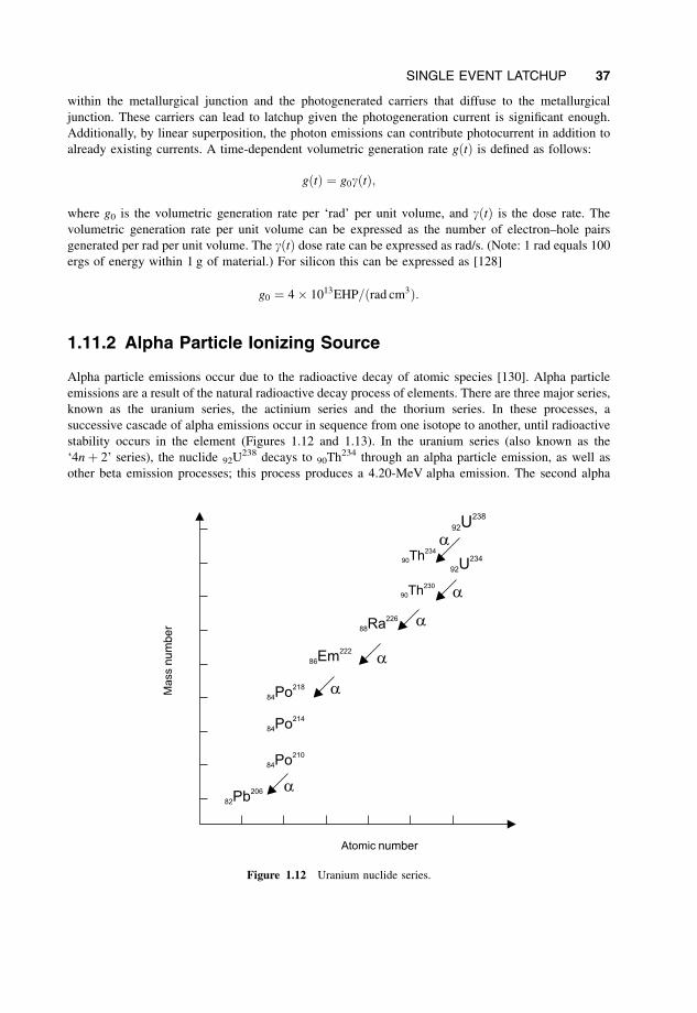
within the metallurgical junction and the photogenerated carriers that diffuse to the metallurgical
junction. These carriers can lead to latchup given the photogeneration current is significant enough.
Additionally, by linear superposition, the photon emissions can contribute photocurrent in addition to
already existing currents. A time-dependent volumetric generation rate gðtÞ is defined as follows:
gðtÞ ¼ g0gðtÞ;
where g0 is the volumetric generation rate per ‘rad’ per unit volume, and gðtÞ is the dose rate. The
volumetric generation rate per unit volume can be expressed as the number of electron–hole pairs
generated per rad per unit volume. The gðtÞ dose rate can be expressed as rad/s. (Note: 1 rad equals 100
ergs of energy within 1 g of material.) For silicon this can be expressed as [128]
g0 ¼ 4 1013EHP=ðrad cm3Þ:
1.11.2 Alpha Particle Ionizing Source
Alpha particle emissions occur due to the radioactive decay of atomic species [130]. Alpha particle
emissions are a result of the natural radioactive decay process of elements. There are three major series,
known as the uranium series, the actinium series and the thorium series. In these processes, a
successive cascade of alpha emissions occur in sequence from one isotope to another, until radioactive
stability occurs in the element (Figures 1.12 and 1.13). In the uranium series (also known as the
‘4n þ 2’ series), the nuclide 92U238 decays to 90Th
234 through an alpha particle emission, as well as
other beta emission processes; this process produces a 4.20-MeV alpha emission. The second alpha
number
num
ber
Figure 1.12 Uranium nuclide series.
SINGLE EVENT LATCHUP 37
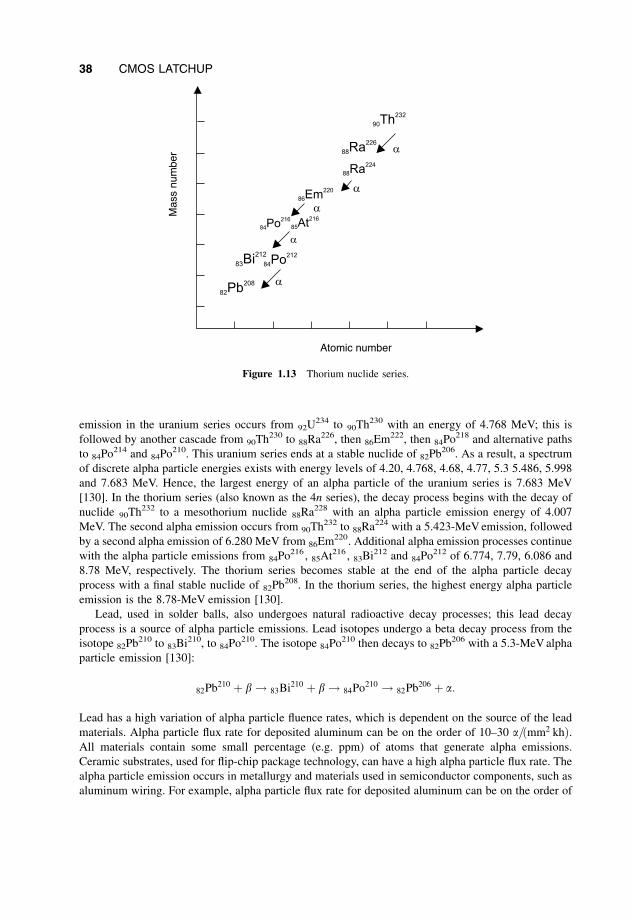
emission in the uranium series occurs from 92U234 to 90Th
230 with an energy of 4.768 MeV; this is
followed by another cascade from 90Th230 to 88Ra
226, then 86Em222, then 84Po
218 and alternative paths
to 84Po214 and 84Po
210. This uranium series ends at a stable nuclide of 82Pb206. As a result, a spectrum
of discrete alpha particle energies exists with energy levels of 4.20, 4.768, 4.68, 4.77, 5.3 5.486, 5.998
and 7.683 MeV. Hence, the largest energy of an alpha particle of the uranium series is 7.683 MeV
[130]. In the thorium series (also known as the 4n series), the decay process begins with the decay of
nuclide 90Th232 to a mesothorium nuclide 88Ra
228 with an alpha particle emission energy of 4.007
MeV. The second alpha emission occurs from 90Th232 to 88Ra
224 with a 5.423-MeVemission, followed
by a second alpha emission of 6.280 MeV from 86Em220. Additional alpha emission processes continue
with the alpha particle emissions from 84Po216, 85At
216 , 83Bi212 and 84Po
212 of 6.774, 7.79, 6.086 and
8.78 MeV, respectively. The thorium series becomes stable at the end of the alpha particle decay
process with a final stable nuclide of 82Pb208. In the thorium series, the highest energy alpha particle
emission is the 8.78-MeV emission [130].
Lead, used in solder balls, also undergoes natural radioactive decay processes; this lead decay
process is a source of alpha particle emissions. Lead isotopes undergo a beta decay process from the
isotope 82Pb210 to 83Bi
210, to 84Po210. The isotope 84Po
210 then decays to 82Pb206 with a 5.3-MeValpha
particle emission [130]:
82Pb210 þ b ! 83Bi
210 þ b ! 84Po210 ! 82Pb
206 þ a:
Lead has a high variation of alpha particle fluence rates, which is dependent on the source of the lead
materials. Alpha particle flux rate for deposited aluminum can be on the order of 10–30 a=ðmm2 khÞ.All materials contain some small percentage (e.g. ppm) of atoms that generate alpha emissions.
Ceramic substrates, used for flip-chip package technology, can have a high alpha particle flux rate. The
alpha particle emission occurs in metallurgy and materials used in semiconductor components, such as
aluminum wiring. For example, alpha particle flux rate for deposited aluminum can be on the order of
Atomic number
Mas
s nu
mbe
r
Figure 1.13 Thorium nuclide series.
38 CMOS LATCHUP
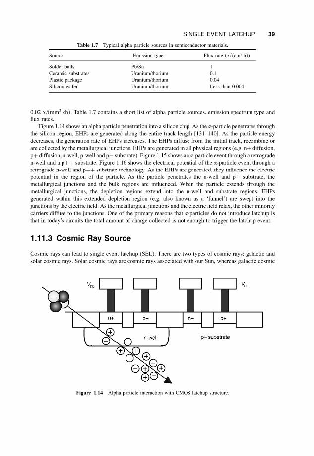
0.02 a=ðmm2 khÞ. Table 1.7 contains a short list of alpha particle sources, emission spectrum type and
flux rates.
Figure 1.14 shows an alpha particle penetration into a silicon chip. As the a-particle penetrates throughthe silicon region, EHPs are generated along the entire track length [131–140]. As the particle energy
decreases, the generation rate of EHPs increases. The EHPs diffuse from the initial track, recombine or
are collected by the metallurgical junctions. EHPs are generated in all physical regions (e.g. nþ diffusion,
pþ diffusion, n-well, p-well and p substrate). Figure 1.15 shows an a-particle event through a retrograden-well and a pþþ substrate. Figure 1.16 shows the electrical potential of the a-particle event through a
retrograde n-well and pþþ substrate technology. As the EHPs are generated, they influence the electric
potential in the region of the particle. As the particle penetrates the n-well and p substrate, the
metallurgical junctions and the bulk regions are influenced. When the particle extends through the
metallurgical junctions, the depletion regions extend into the n-well and substrate regions. EHPs
generated within this extended depletion region (e.g. also known as a ‘funnel’) are swept into the
junctions by the electric field. As the metallurgical junctions and the electric field relax, the other minority
carriers diffuse to the junctions. One of the primary reasons that a-particles do not introduce latchup is
that in today’s circuits the total amount of charge collected is not enough to trigger the latchup event.
1.11.3 Cosmic Ray Source
Cosmic rays can lead to single event latchup (SEL). There are two types of cosmic rays: galactic and
solar cosmic rays. Solar cosmic rays are cosmic rays associated with our Sun, whereas galactic cosmic
Table 1.7 Typical alpha particle sources in semiconductor materials.
Source Emission type Flux rate (a=ðcm2 hÞ)
Solder balls Pb/Sn 1
Ceramic substrates Uranium/thorium 0.1
Plastic package Uranium/thorium 0.04
Silicon wafer Uranium/thorium Less than 0.004
Figure 1.14 Alpha particle interaction with CMOS latchup structure.
SINGLE EVENT LATCHUP 39

rays are from a source beyond our solar system. These cosmic rays are classified into three groups –
primary cosmic rays, cascade cosmic rays and sea-level cosmic rays. Primary cosmic rays are cosmic
rays that exist outside of our Earth’s atmosphere, which have not undergone collision processes. The
‘cascade cosmic rays’ are the cosmic rays that are generated after a primary cosmic ray enters the
Earth’s atmosphere. When a primary cosmic ray enters the Earth’s atmosphere, it undergoes a series of
particle collisions leading to a plethora of particle events. Sea-level cosmic rays are the cosmic rays
observed on the Earth.
Galactic particles consist of protons, alpha particles and heavy ions. Galactic particles are 92 %
protons, 6 % alpha particles and 2 % heavy ions. Heavy ions consist of O, N, C, B, Be, Li and He. The
Figure 1.15 Alpha particle simulation electrostatic potential distribution results through a CMOS structure
consisting of a retrograde n-well and pþþ substrate.
Figure 1.16 Alpha particle simulation electrostatic potential distribution time sequence through a CMOS
structure consisting of a retrograde n-well and pþþ substrate.
40 CMOS LATCHUP
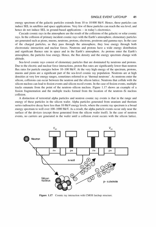
energy spectrum of the galactic particles extends from 10 to 10 000 MeV. Hence, these particles can
induce SEL in satellites and space applications. Very few of these particles can reach the sea level, and
hence do not induce SEL in ground-based applications – in today’s electronics.
Cascade cosmic rays in the atmosphere are the result of the collisions of the galactic or solar cosmic
rays. In the collision of primary incident cosmic rays with the Earth’s atmosphere, elementary particles
are generated such as pions, muons, neutrons, protons, electrons, positrons and gamma rays. In the case
of the charged particles, as they pass through the atmosphere, they lose energy through both
electrostatic interaction and nuclear forces. Neutrons and protons have a wide energy distribution
and significant fluence rate in space and in the Earth’s atmosphere. As protons enter the Earth’s
atmosphere, the particles lose energy. Hence, the flux density and the energy spectrum change with
altitude.
Sea-level cosmic rays consist of elementary particles that are dominated by neutrons and protons.
Due to the electric and nuclear force interactions, proton flux rates are significantly lower than neutron
flux rates for particle energies below 10–100 MeV. At the very high energy of the spectrum, protons,
muons and pions are a significant part of the sea-level cosmic ray population. Neutrons are at high
densities at very low energy ranges, sometimes referred to as ‘thermal neutrons’. As neutrons enter the
silicon, collisions can occur between the neutron and the silicon lattice. Neutrons that collide with the
silicon nucleus can lead to fission events and silicon recoil events. In the case of fission events, multiple
tracks emanate from the point of the neutron–silicon nucleus. Figure 1.17 shows an example of a
fission fragmentation and the multiple tracks formed from the location of the neutron–Si nucleus
collision.
A distinction of terrestrial alpha particles and neutron cosmic ray events is that in the range and
energy of these particles in the silicon wafer. Alpha particles generated from uranium and thorium
series radioactive decay have less than 10-MeVenergy levels, where the cosmic ray spectrum is a broad
energy spectrum to well over 100–1000 MeV. As a result, the alpha particle events occur only near the
surface of the devices (except those generated from the silicon wafer itself). In the case of neutron
events, no carriers are generated in the wafer until a collision event occurs with the silicon lattice.
Figure 1.17 Cosmic ray interaction with CMOS latchup structure.
SINGLE EVENT LATCHUP 41
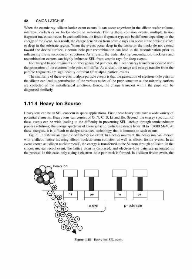
When the cosmic ray–silicon lattice event occurs, it can occur anywhere in the silicon wafer volume,
interlevel dielectrics or back-end-of-line materials. During these collision events, multiple fission
fragment tracks can occur. In each collision, the fission fragment type can be different depending on the
energy of the event. As a result, the charge generation from cosmic rays can occur at the device surface
or deep in the substrate region. When the events occur deep in the lattice or the tracks do not extend
toward the device surface, electron–hole pair recombination can lead to the recombination prior to
influencing the semiconductor structures. As a result, the wafer doping concentration, thickness and
recombination centers can highly influence SEL from cosmic rays for deep events.
For charged fission fragments or other generated particles, the linear energy transfer associated with
the generation of the electron–hole pairs will differ. As a result, the range and energy transfer from the
particle fragments are significantly different from alpha particle events.
The similarity of these events to alpha particle events is that the generation of electron–hole pairs in
the silicon can lead to perturbation of the various nodes of the pnpn structure as the minority carriers
are collected at the metallurgical junctions. Hence, the charge transport within the pnpn can be
diagnosed similarly.
1.11.4 Heavy Ion Source
Heavy ions can be an SEL concern in space applications. First, these heavy ions have a wide variety of
potential elements. Heavy ions can consist of O, N, C, B, Li and He. Second, the energy spectrum of
these events can be wide leading to the difficulty in preventing SEL latchup through semiconductor
process solutions; the energy spectrum of these galactic particles extends from 10 to 10 000 MeV. At
these energies, it is difficult to design advanced technology that is immune to such events.
Figure 1.18 shows an example of a heavy ion event. In a heavy ion event, the heavy ion can interact
with a silicon lattice inducing silicon nucleus–atom collision, as well as silicon fission events. In an
event known as ‘silicon nuclear recoil’, the energy is transferred to the Si atom through collision. In the
silicon nuclear recoil event, the lattice atom is displaced, and electron–hole pairs are generated in
the process. In this case, only a single electron–hole pair track is formed. In a silicon fission event, the
Figure 1.18 Heavy ion SEL event.
42 CMOS LATCHUP
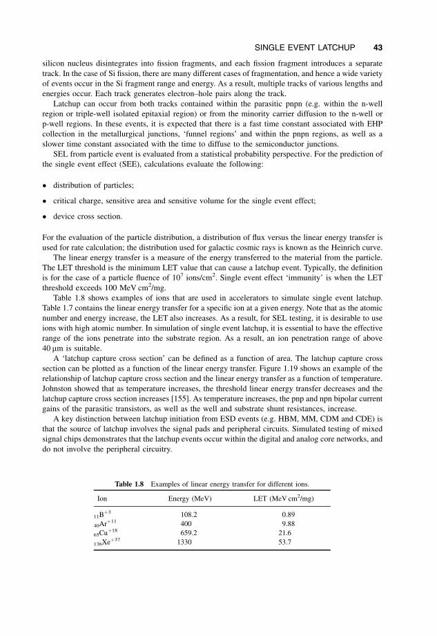
silicon nucleus disintegrates into fission fragments, and each fission fragment introduces a separate
track. In the case of Si fission, there are many different cases of fragmentation, and hence a wide variety
of events occur in the Si fragment range and energy. As a result, multiple tracks of various lengths and
energies occur. Each track generates electron–hole pairs along the track.
Latchup can occur from both tracks contained within the parasitic pnpn (e.g. within the n-well
region or triple-well isolated epitaxial region) or from the minority carrier diffusion to the n-well or
p-well regions. In these events, it is expected that there is a fast time constant associated with EHP
collection in the metallurgical junctions, ‘funnel regions’ and within the pnpn regions, as well as a
slower time constant associated with the time to diffuse to the semiconductor junctions.
SEL from particle event is evaluated from a statistical probability perspective. For the prediction of
the single event effect (SEE), calculations evaluate the following:
distribution of particles;
critical charge, sensitive area and sensitive volume for the single event effect;
device cross section.
For the evaluation of the particle distribution, a distribution of flux versus the linear energy transfer is
used for rate calculation; the distribution used for galactic cosmic rays is known as the Heinrich curve.
The linear energy transfer is a measure of the energy transferred to the material from the particle.
The LET threshold is the minimum LET value that can cause a latchup event. Typically, the definition
is for the case of a particle fluence of 107 ions/cm2. Single event effect ‘immunity’ is when the LET
threshold exceeds 100 MeV cm2/mg.
Table 1.8 shows examples of ions that are used in accelerators to simulate single event latchup.
Table 1.7 contains the linear energy transfer for a specific ion at a given energy. Note that as the atomic
number and energy increase, the LET also increases. As a result, for SEL testing, it is desirable to use
ions with high atomic number. In simulation of single event latchup, it is essential to have the effective
range of the ions penetrate into the substrate region. As a result, an ion penetration range of above
40 mm is suitable.
A ‘latchup capture cross section’ can be defined as a function of area. The latchup capture cross
section can be plotted as a function of the linear energy transfer. Figure 1.19 shows an example of the
relationship of latchup capture cross section and the linear energy transfer as a function of temperature.
Johnston showed that as temperature increases, the threshold linear energy transfer decreases and the
latchup capture cross section increases [155]. As temperature increases, the pnp and npn bipolar current
gains of the parasitic transistors, as well as the well and substrate shunt resistances, increase.
A key distinction between latchup initiation from ESD events (e.g. HBM, MM, CDM and CDE) is
that the source of latchup involves the signal pads and peripheral circuits. Simulated testing of mixed
signal chips demonstrates that the latchup events occur within the digital and analog core networks, and
do not involve the peripheral circuitry.
Table 1.8 Examples of linear energy transfer for different ions.
Ion Energy (MeV) LET (MeV cm2/mg)
11Bþ3 108.2 0.89
40Arþ11 400 9.88
65Cuþ18 659.2 21.6
136Xeþ37 1330 53.7
SINGLE EVENT LATCHUP 43
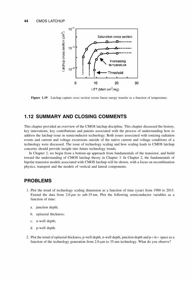
1.12 SUMMARY AND CLOSING COMMENTS
This chapter provided an overview of the CMOS latchup discipline. This chapter discussed the history,
key innovations, key contributions and patents associated with the process of understanding how to
address the latchup issue in semiconductor technology. Both issues associated with ionizing radiation
events and current and voltage excursions outside of the native current and voltage conditions of a
technology were discussed. The issue of technology scaling and how scaling leads to CMOS latchup
concerns should provide insight into future technology trends.
In Chapter 2, we begin from a bottom-up approach from fundamentals of the transistor, and build
toward the understanding of CMOS latchup theory in Chapter 3. In Chapter 2, the fundamentals of
bipolar transistor models associated with CMOS latchup will be shown, with a focus on recombination
physics, transport and the models of vertical and lateral components.
PROBLEMS
1. Plot the trend of technology scaling dimension as a function of time (year) from 1980 to 2015.
Extend the data from 2.0 mm to sub-35 nm. Plot the following semiconductor variables as a
function of time:
a. junction depth;
b. epitaxial thickness;
c. n-well depth;
d. p-well depth.
2. Plot the trend of epitaxial thickness, p-well depth, n-well depth, junction depth and pþ/nþ space as a
function of the technology generation from 2.0-mm to 35-nm technology. What do you observe?
Figure 1.19 Latchup capture cross section versus linear energy transfer as a function of temperature.
44 CMOS LATCHUP

3. Given a metric of the ‘beta product’, derive the scaling of the beta product as a function of the
scaling variable a. Assume an original beta product value of ðbnpnÞ0ðbpnpÞ0. Assume MOSFET
constant electric field scaling theory. How does it scale?
4. Given that a technology must maintain the ‘beta product’ equal to unity, how would one provide a
‘constant latchup robustness scaling’ value as a technology is scaled according to MOSFET
constant electric field scaling theory. By constant latchup robustness scaling, the latchup
robustness is preserved as a constant as the technology is scaled as scaling parameter a. (Hint:
Invent a second scaling parameter to offset the natural scaling and show the relationship of the new
scaling parameter as a function of the MOSFET constant electric field scaling parameter.)
5. Plot the trend of substrate resistance as a function of technology generation from 2.0 mm to 35 nm.
Define a relationship of the trend. Assuming that a constant substrate resistance must be
maintained between a pþ substrate contact and an n-channel transistor, show the derivation for
the spacing between the substrate contact and the transistor.
6. Given a standard industry cable (category 5 or 6 LAN cable), provide an estimate of the range
of typical capacitance per unit length values. Plot total capacitance of a cable as a function of
the cable length from 1 to 300 ft (in pF). Given these cables are charged through triboelectric
charging to 100 V, what is the total stored charge in the cable for 1, 10, 20, 50, 100, 200 and
300 ft lengths.
7. Given a charged cable, the width of a pulse from the cable is proportional to the length of the cable.
Calculate the pulse width from a category 5 or 6 cable for cables in the range of 1–300 ft.
8. Given a JEDEC latchup specification of 100 mA current, derive the relationship of a cable that
provides a pulse of this magnitude as a function of capacitance per unit length, cable length and
predischarge voltage.
9. The range of an alpha particle in silicon can be calculated as a function of the particle:
R ¼ 1:53E1:67;
where E is the energy in MeV and R is the range in microns. Plot the range as a function of the
energy from 1 to 10 MeV. Given a uranium series, the maximum energy is 8.8 MeV. Calculate the
range of the highest energy alpha particle. Given all the charge along the range is collected at a
given junction (e.g. an n-well-to-substrate junction), what is the number of electron–hole pairs
generated and what is the total charge?
10. The range of an alpha particle in silicon can be calculated as a function of the particle:
R ¼ 1:53E1:67;
where E is the energy in MeV and R is the range in microns. Plot the range as a function of the
energy from 1 to 10 MeV. Given a lead solder ball, the maximum energy is 5.5 MeV. Calculate the
maximum range of the alpha particle emission. What is the range of energy emitted? Why? Given
all the charge along the range is collected at a given junction (e.g. an n-well-to-substrate junction),
what is the number of electron–hole pairs generated and what is the total charge?
11. Given an ionizing radiation source generates electron–hole pairs in the base region of a bipolar
transistor. Explain the transport and the collection processes of both the electron and the hole.
PROBLEMS 45

12. Show the difference in the interaction from alpha particles, cosmic ray events and heavy ion
events. Where does the interaction occur? How does the time response and spatial dependencies
differ? How does this affect the time response of the drift and diffusion processes? Which
processes have ‘funneling’ and why?
REFERENCES
1. J.L. Moll, M. Tannenbaum, J.M. Goldey and N. Holonyak. P-N-P-N transistor switches. Proceedings of the IRE,
44, 1956, 1174–1182.
2. A.K. Jonscher. P-N-P-N switching diodes. Journal of Electronic and Control, 3, 1957, 573–586.
3. F.E. Gentry, F.W. Gutzwiller, N. Holonyak and E.E. von Zastrow. Semiconductor Controlled Rectifiers:
Principles and Applications of p-n-p-n Devices. Englewood Cliffs, NJ: Prentice-Hall; 1964.
4. H.A. Schafft. Second breakdown – a comprehensive review. Proceeding of the IEEE, 55, 1967, 1272–
1288.
5. J.E. Lilienfeld. US Patent No. 1,745,175 (1930).
6. O. Heil. UK Patent No. 439,457.
7. K. Kinoshita, C.T. Kleiner and E.D. Johnson. Radiation induced regeneration through the p–n junction isolation
monolithic IC’s. IEEE Transactions on Nuclear Science, 12, 1965, 83–90.
8. R.A. Poll and J.F. Leavy. Study of transient radiation induced latchup. General Atomic Division Final Report
(Contract N0014-66-C-0347), No. GA-7969, May 1967.
9. J.F. Leavy and R.A. Poll. Radiation-induced integrated circuit latchup. IEEE Transactions on Nuclear Science,
16, 1969, 96–103.
10. W.J. Dennehy, A.G. Holmes-Seidle and W.F. Leopold. Transient radiation response of complementary-
symmetry MOS integrated circuits. IEEE Transactions on Nuclear Science, 16, 1969, 114–119.
11. S.S. Eaton. Noise immunity of COS/MOS integrated-circuit logic gates. RCA Application Note ICA-6176,
Harrison, NJ, 1970.
12. B.L. Gregory and B.D. Shafer. Latchup in CMOS integrated circuits. IEEE Transactions on Nuclear Science, 20,
1973, 293–299.
13. B.L. Gregory. Latchup studies in bulk silicon CMOS integrated circuits. Sandia Laboratory Report No. 73-3003,
Albuquerque, NM, January 20, 1973.
14. B.D. Shafer. CMOS latchup analysis and prevention. Sandia Laboratories Report SAND75-0371, Albuquerque,
NM, June 1975.
15. L.J. Gallace and H.L. Pujol. Reliability considerations for COS/MOS devices. RCA Technical Note ST-6418,
RCA Corporation, Somerville, NJ, July 1975.
16. C.E. Barnes, W.R. Dawes Jr., G.F. Debenwick, B.L. Gregory, C.B. Norris Jr., H.H. Sander and B.D. Shafer.
Latchup prevention in CMOS. Sandia Laboratories Report SAND76-0048, Albuquerque, NM, March 1976.
17. D.R. Alexander, R.M. Turfler and L.D. Ray. MOS modeling: Part II. BDM Corp. Report BDM/A-207-75-TR-R2,
Albuquerque, NM, September 30, 1976.
18. G.J. Brucker. Characteristics of CMOS/bulk and SOS memories in a transient environment. IEEE Transactions
on Nuclear Science, 24, 1977, 2209–2212.
19. F.N. Coppage and D.C. Evans. Characteristics of destruction from latchup in CMOS. IEEE Transactions on
Nuclear Science, 24, 1977, 2226–2229.
20. A. London and R.C. Wang. Dose rate and extended total dose characterization of radiation hardened metal gate
CMOS integrated circuits. IEEE Transactions on Nuclear Science, 25, 1978, 1172–1175.
21. M. Simons. Radiation effects in MOS integrated circuits. Final Technical Report RTI/0991/00-03F, Research
Triangle Institute, Research Triangle Park, NC, February 1978.
22. L.W. Ricketts. Fundamentals of Nuclear Hardening of Electronic Equipment. New York: Wiley-Interscience;
1972.
23. K. Stephenson. CMOS: some application guidelines. Harris Semiconductor Application Note 209, Harris
Semiconductor, Melbourne, FL, March 1975.
24. L.L. Sivo, F. Rosen and L.C. Jeffers. Latchup screening of LSI devices. IEEE Transactions on Nuclear Science,
25, 1978, 1534–1537.
46 CMOS LATCHUP
25. J.L. Crowley, F.A. Junga and T.J. Stultz. Technique for selection of transient radiation-hard junction-isolated
integrated circuits. IEEE Transactions on Nuclear Science, 23, 1976, 1703–1708.
26. T.J. Stultz, F.A. Junga and J.L. Crowley. Radiation-induced latchup of junction isolated integrated circuits.
Lockheed Palo Alto Research Laboratory Report LMSC-D497933, Palo Alto, CA, March 20, 1976.
27. J.R. Adams and R.J. Sokel. Neutron irradiation for prevention of latchup in CMOS integrated circuits. IEEE
Transactions on Nuclear Science, 26, 1979, 5069–5073.
28. W.R. Dawes Jr. and G.F. Derbenwick. Prevention of CMOS latchup by gold doping. IEEE Transactions on
Nuclear Science, 23, 1976, 2027–2030.
29. D.B. Estreich, A. Ochoa Jr. and R.W. Dutton. An analysis of latchup prevention in CMOS IC’s using an epitaxial-
buried layer process. International Electron Device Meeting (IEDM) Technical Digest, December 1978.
p. 230–234.
30. D.B. Estreich and R.W. Dutton. Modeling latchup in CMOS integrated circuits. 1978 Asilomar Conference on
Circuits, Systems, and Computer Digest, Monterey, CA, November 1978. p. 489–492.
31. D.B. Estreich and R.W. Dutton. Latchup in CMOS integrated circuits. 1978 Government Microcircuit
Applications Conference (GOMAC) Digest of Papers, Monterey, CA, November 1978. p. 110–111.
32. D.B. Estreich. Latchup and radiation integrated circuit (LURIC): a test chip for CMOS latchup investigation.
Sandia Laboratories Report SAND78-1540, Albuquerque, NM, November 1978.
33. D.B. Estreich. The physics and modeling of latch-up and CMOS integrated circuits. Technical Report
No. G-201-9, Integrated Circuits Laboratory, Stanford Electronic Laboratories, Stanford University, Stanford,
CA, November 1980.
34. P.V. Dressendorfer and M.G. Armendariz. A SEM technique for experimentally locating latchup paths in
integrated circuits. IEEE Transactions on Nuclear Science, 27, 1980, 1688–1693.
35. J.E. Schroder, A. Ochoa and P.V. Dressendorfer. Latchup elimination in bulk CMOS LSI circuits. IEEE
Transactions on Nuclear Science, 27, 1980, 1735–1738.
36. R.S. Payne, W.R. Grant and W.J. Bertram. Elimination of latchup in bulk CMOS. International Electron Device
Meeting (IEDM) Technical Digest, December 1980. p. 248–251.
37. W.D. Raburn. A model for parasitic SCR in bulk CMOS. International Electron Device Meeting (IEDM)
Technical Digest, December 1980. p. 252–255.
38. R.D. Rung, C.J. Delloca and L.G. Walker. A retrograde p-well for higher density CMOS. IEEE Transactions on
Electron Devices, 28(10), 1980, 1115–1119.
39. L. Parillo, et al. Twin-tub CMOS – a technology for VLSI circuits. International Electron Device Meeting
(IEDM) Technical Digest, 1980. p. 752–755.
40. S.R. Combs. Scaleable retrograde p-well CMOS technology. International Electron Device Meeting (IEDM)
Technical Digest, December 1981. p. 346–349.
41. T. Iizuka and J. Moll. A figure of merit for CMOS latchup tolerance. The 1981 CMOS Workshop, San Francisco
Airport Hilton, San Francisco, CA, May 18, 1981.
42. P.V. Dressendorfer and A. Ochoa. An analysis of modes of operation of parasitic SCR’s. IEEE Transactions on
Nuclear Science, 28(6), 1981, 4288–4291.
43. A. Ochoa and P.V. Dressendorfer. A discussion of the role of distributed effects in latchup. IEEE Transactions on
Nuclear Science, 28(6), 1981, 4292–4294.
44. A.W. Wieder, C. Werner and J. Harter. Design model for bulk CMOS scaling enabling accurate latchup
prediction. International Electron Device Meeting (IEDM) Technical Digest, 1981. p. 354–357.
45. G.J. Hu, M.R. Pinto and S. Kordic. Two-dimensional simulation of latchup in CMOS structure. Device Research
Conference Proceedings, VA-5, June 21–23, 1982.
46. R.D. Rung and H. Momose. Improved modeling of CMOS latchup and VLSI implications. Symposium on VLSI
Technology, September 1982. p. 52–53.
47. R.D. Rung, H. Momose and Y. Nagabuko. Deep trench isolated CMOS devices. International Electron Device
Meeting (IEDM) Technical Digest, 1982. p. 237–240.
48. C.C. Huang, M.D. Hartanft, N.F. Pu, C. Yue, C. Rahn, J. Schrankler, G.D. Kirchner, F.L. Hampton and T.E.
Hendrickson. Characterization of CMOS latchup. International Electron Device Meeting (IEDM) Technical
Digest, 1982. p. 454–457.
49. R.R. Troutman and H.P. Zappe. Power-up triggering condition for latchup in bulk CMOS. 1982 Symposium on
VLSI Technology, Oiso, Japan, September 1982. p. 52–53.
REFERENCES 47
50. R.R. Troutman and H.P. Zappe. A transient analysis of latchup in bulk CMOS. IEEE Transactions on Electron
Devices, 30, 1983, 170–179.
51. R.D. Rung and H. Momose. DC holding and dynamic triggering characteristics of bulk CMOS latchup. IEEE
Transactions on Electron Devices, 30, 1983, 1647–1655.
52. U. Schwabe, H. Herbst, E.J. Jacobs and D. Takacs. N- and p-well optimization for high-speed n-epitaxy CMOS
circuits. IEEE Transactions on Electron Devices, 30, 1983, 1339–1344.
53. D.L. Wollesen, J. Haskell and J. Yu. N-well and p-well performance comparison. International Electron Device
Meeting (IEDM) Technical Digest, 1983. p. 31–34.
54. G. Goto, H. Takahashi and T. Nakamura. Latchup immunity against noise pulses in a CMOS double well
structure. International Electron Device Meeting (IEDM) Technical Digest, 1983. p. 168–171.
55. G.J. Hu, Y. Taur, R.H. Dennard, L.M. Terman and C.Y. Ting. A self-aligned 1-mm CMOS technology for VLSI.
International Electron Device Meeting (IEDM) Technical Digest, 1983. p. 731–734.
56. D. Takacs, J. Harter, E.P. Jacobs, C. Werner, U. Schwabe, J. Winnerl and E. Lange. Comparison of latchup
in n-well and p-well CMOS circuits. International Electron Device Meeting (IEDM) Technical Digest, 1983.
p. 159–164.
57. J. Manoliu, F.H. Tseng, B.J. Woo and T.J. Meier. High density and reduced latchup susceptibility CMOS
technology for VLSI. IEEE Electron Device Letters, 4, 1983, 233–235.
58. L. Wakeman. Silicon gate CMOS chips gain immunity to SCR latchup. Electronics, 56(16), 1983, 136–140.
59. R.R. Troutman. Epitaxial layer enhancement of n-well guard rings for CMOS circuits. IEEE Electron Device
Letters, 4, 1983, 438–440.
60. Y. Niitsu, H. Nihara, K. Kanzaki and S. Kohyama. Resistance modulation effect due to current injection and
CMOS latchup. International Electron Device Meeting (IEDM) Technical Digest, 1983. p. 164–167.
61. E. Hamdy and A. Mohsen. Characterization and modeling of transient latchup in CHMOS technology.
International Electron Device Meeting (IEDM) Technical Digest, 1983. p. 172–175.
62. R.R. Troutman and M.J. Hargrove. Transmission line model for latchup in CMOS circuits. Symposium on VLSI
Technology, September 13–15, 1983. p. 56–59.
63. G.J. Hu. A better understanding of CMOS latchup. IEEE Transactions on Electron Devices, 31, 1984,
62–67.
64. R.C. Fang and J.L. Moll. Latchup model for the parasitic path in bulk CMOS. IEEE Transactions on Electron
Devices, 31, 1984, 113–120.
65. W. Craig. Latchup test structures and their characterization. IEEE VLSI Workshop on Test Structures, San Diego,
February 20, 1984.
66. J.G. Dooley and R.C. Jaeger. Temperature dependence of latchup in CMOS circuits. IEEE Electron Device
Letters, 5, 1984, 41–43.
67. D. Takacs, C. Werner, J. Harter and U. Schwabe. Surface induced latchup in VLSI CMOS circuits. IEEE
Transactions on Electron Devices, 31, 1984, 279–286.
68. R.R. Troutman and H.P. Zappe. Layout and bias considerations for preventing transiently triggered latchup in
CMOS. IEEE Transactions on Electron Devices, 31, 1984, 279–286.
69. I.H. Leventhal. Comparison of DC latchup characterization techniques for CMOS technology. BS thesis,
Massachusetts Institute of Technology, June 1984.
70. G.J. Hu and R.H. Bruce. A CMOS structure with high holding voltage. IEEE Electron Device Letters, 5, 1984,
211–214.
71. K.W. Terrill and C. Hu. Substrate resistance calculation for latchup modeling. IEEE Transactions on Electron
Devices, 31, 1984, 1152–1155.
72. K.W. Terrill, P.F. Byrne, H.P. Zappe, N.W. Cheung and C. Hu. A new method for preventing CMOS latchup.
International Electron Device Meeting (IEDM) Technical Digest, 1984. p. 406–409.
73. A.G. Lewis. Latchup suppression in fine dimension shallow p-well CMOS circuits. IEEE Transactions on
Electron Devices, 31, 1984, 1472–1481.
74. U. Schwabe, E.P. Jacobs, D. Takacs, J. Winnerl and E. Lange. Reduced nþ/pþ spacing with high latchup
hardness in self-aligned double well CMOS technology. International Electron Device Meeting (IEDM)
Technical Digest, 1984. p. 410–413.
75. S. Odanaka, M. Wakabayashi and T. Ohzone. The dynamics of latchup turn-on behavior in scaled CMOS. IEEE
Transactions on Electron Devices, 32, 1985, 1334–1340.
48 CMOS LATCHUP
76. M.R. Pinto and R.W. Dutton. Accurate triggering condition analysis for CMOS latchup. IEEE Electron Device
Letters, 6(2), 1985, 100–102.
77. K.Y. Fu. Transient latchup in bulk CMOS with a voltage-dependent well–substrate junction capacitance. IEEE
Transactions on Electron Device Letters, 32, 1985, 717–720.
78. J.E. Hall, J.A. Seitchik, L.A. Arledge and P. Yang. An improved circuit model for CMOS latchup. IEEE Electron
Device Letters, 6, 1985, 320–322.
79. R. Troutman. Latchup in CMOS Technology: The Problem and the Cure. New York: Kluwer Academic
Publishers; 1985.
80. P. Cottrell, S. Warley, S. Voldman, W. Leipold and C. Long. N-well design for trench DRAM arrays.
International Electron Device Meeting (IEDM) Technical Digest, December 1988. p. 584–587.
81. S. Voldman, M. Marceau, A. Baker, E. Adler, S. Geissler, J. Slinkman, J.B. Johnson and M. Paggi. Retrograde
well and epitaxial thickness optimization for shallow- and deep-trench collar merged isolation and node trench
(MINT) SPT cell and CMOS logic technology. International Electron Device Meeting (IEDM) Technical Digest,
1992. p. 811–814.
82. S. Voldman. Retrograde well implants and ESD. SEMATECH Vertical Modulated Well PTAB, November,
Austin, TX, November 1994.
83. S. Voldman. Optimization of MeV retrograde wells for advanced logic and microprocessor/PowerPC
and electrostatic discharge (ESD). Smart and Economic Device and Process Designs for ULSI Using MeV
Implant Technology Seminar: SEMICON West, SEMICON West GENUS Seminar, San Francisco, CA,
July 1994.
84. S. Voldman. MeV implants boost device design. IEEE Circuits and Devices 1995, 11(6), 8–16.
85. S. Voldman. The impact of MOSFET technology evolution and scaling on electrostatic discharge protection.
Microelectronics Reliability, 38, 1998, 1649–1668.
86. S. Voldman. Electrostatic discharge protection, scaling, and ion implantation in advanced semiconductor
technologies. Process Integration Issues/Technical Trends Session, Proceedings of the Ion Implantation
Conference (I2CON), Napa, CA, 1999.
87. M. Hargrove, S. Voldman, J. Brown, K. Duncan andW. Craig. Latchup in CMOS technology. Proceedings of the
International Reliability Physics Symposium (IRPS), 1998. p. 269–278.
88. T. Li and S.M. Kang. Layout extraction and verification methodology for CMOS I/O circuits. IEEE/ACM Design
Automation Conference (DAC), 1998. p. 291–296.
89. T. Li. Design automation for reliable CMOS chip I/O circuits. PhD thesis, University of Illinois Urbana-
Champaign, UILU-ENG-98-2219, August 1998.
90. T. Li, C.H. Tsai, E. Rosenbaum and S.M. Kang. Substrate modeling and lumped substrate resistance
extraction for latchup/ESD circuit simulations. IEEE/ACM Design Automation Conference (DAC), 1999.
p. 549–554.
91. K.K. Bourdelle, Y. Chen, R. Ashton, L. Rubin, A. Agarwal and W. Morris. Epi-replacement in CMOS
Technology by high dose, high energy boron implantation into Cz substrates. International Electron Device
Meeting (IEDM) Technical Digest, 1999. p. 312–316.
92. W. Morris. Latchup in CMOS. Proceedings of the International Reliability Physics Symposium (IRPS), 2003.
p. 76–84.
93. G. Boselli, V. Reddy and C. Duvvury. Latchup in 65 nm CMOS technology: a scaling perspective. Proceedings
of the International Reliability Physics Symposium (IRPS), 2004. p. 137–144.
94. A. Weger, S. Voldman, F. Stellari, P. Song, P. Sanda and M. McManus. A transmission line pulse (TLP)
picosecond imaging circuit analysis (PICA) methodology for evaluation of ESD and latchup. Proceedings of the
International Reliability Physics Symposium (IRPS), 2003. p. 99–104.
95. F. Stellari, P. Song,M.K.McManus, A.J.Weger, K. Chatty, M.Muhammad and P. Sanda. Study of critical factors
determining latchup sensitivity in ICs using emission microscopy. Proceeding of the International Symposium
for Testing and Failure Analysis (ITSFA), 2003. p. 19–24.
96. K. Chatty, P. Cottrell, M. Muhammad, F. Stellari, A. Weger, P. Song and M. McManus. Model-based guidelines
for cable discharge events (CDE) induced latchup in CMOS ICs. Proceedings of the International Reliability
Physics Symposium (IRPS), 2004. p. 130–134.
97. S. Voldman. Latchup and the domino effect. Proceedings of the International Reliability Physics Symposium
(IRPS), 2005. p. 145–156.
REFERENCES 49
98. A. Watson, S. Voldman and T. Larsen. Deep trench guard ring structures and evaluation of the probability of
minority carrier escape for ESD and latchup in advanced BiCMOS SiGe technology. Proceedings of the Taiwan
Electrostatic Discharge Conference (T-ESDC), 2003. p. 97–103.
99. S. Voldman and A. Watson. The influence of deep trench and substrate resistance on the latchup robustness in a
BiCMOS silicon germanium technology. Proceedings of the International Reliability Physics Symposium
(IRPS), 2004. p. 135–142.
100. A. Watson and S. Voldman. The effect of deep trench and sub-collector on the latchup robustness in BiCMOS
silicon germanium technology. Proceedings of the Bipolar Circuit Technology Meeting (BCTM), Montreal,
Canada, September 12–14, 2004. p. 172–175.
101. S. Voldman and A.Watson. The influence of polysilicon-filled deep trench and sub-collector implants on latchup
robustness in RF CMOS and BiCMOS SiGe technology. Proceedings of the Taiwan Electrostatic Discharge
Conference (T-ESDC), 2004. p. 15–19.
102. S. Voldman. A review of CMOS latchup and electrostatic discharge (ESD) in bipolar complimentary MOSFET
(BiCMOS) silicon germanium technologies: Part II. Latchup. Microelectronics and Reliability, 45, 2005,
437–455.
103. S. Voldman, E.G. Gebreselasie, L.W. Lanzerotti, N.B. Feilchenfeld, S.A. St. Onge, A. Joseph and J. Dunn.
The influence of silicon dioxide-filled trench isolation (TI) structure and implanted sub-collector on
latchup robustness. Proceedings of the International Reliability Physics Symposium (IRPS), 2005.
p. 112–121.
104. S. Voldman, E.G. Gebreselasie, D. Hershberger, D.S. Collins, N.B. Feilchenfeld, S.A. St. Onge, A. Joseph,
J. Dunn. Latchup in merged triple well technology. Proceedings of the International Reliability Physics
Symposium (IRPS), 2005. p. 129–136.
105. S. Voldman and E. Gebreselasie. The influence and integration of merged triple well, deep trench, and sub-
collector on CMOS latchup. Proceedings of the Taiwan Electrostatic Discharge Conference (T-ESDC), 2006.
p. 49–52.
106. S. Voldman, E. Gebreselasie, X.F. Liu, D. Coolbaugh and A. Joseph. The influence of high resistivity substrates
on CMOS latchup. Proceedings of the Electrical Overstress/Electrostatic Discharge (EOS/ESD) Symposium,
2005. p. 90–99.
107. J. Salcedo-Suner, R. Cline and C. Duvvury. A new I/O signal latch-up phenomenon in voltage tolerant
ESD protection circuits. Proceedings of the International Reliability Physics Symposium (IRPS), 2003.
p. 85–91.
108. Y. Huh, K.J. Min, P. Bendix, V. Axelrad, R. Narayan, J.-W. Chen, L.D. Johnson and S. Voldman. Chip-level
layout and bias considerations for preventing neighboring I/O cell interaction induced latchup and inter-power
supply latchup in CMOS technologies. Proceedings of the Electrical Overstress/Electrostatic Discharge (EOS/
ESD) Symposium, 2005. p. 100–107.
109. R.Y. Zhan, H.G. Feng, Q. Wu, G. Chen, X.K. Guan and A.Z. Wang. A technology-independent CAD tool for
ESD protection device extraction: ESD Extractor. Proceedings of the International Conference on Computer-
Aided Design, 2002. p. 510–513.
110. R.Y. Zhan. ESDCat: a new CAD software package for full-chip ESD protection circuit verification, October 2005.
111. ESDAssociation. ESD STM 5.1-2001: standard test method for electrostatic discharge sensitivity testing-human
body model (HBM) component level, 2001.
112. ESD Association. ESD STM 5.2-1998: standard test method for electrostatic discharge sensitivity testing-
machine model (MM) component level, 1998.
113. Intel Corporation. Cable discharge event in local area network environment. Intel White Paper, Order
No. 249812-001, July 2001.
114. R. Brooks. A simple model for the cable discharge event. IEEE802.3 Cable-Discharge Ad-Hoc Committee,
March 2001.
115. Telecommunications Industry Association (TIA). Category 6 cabling: static discharge between LAN cabling and
data terminal equipment. Category 6 Consortium, December 2002.
116. J. Deatherage and D. Jones. Multiple factors trigger discharge events in Ethernet LANs, Electronic Design 2000;
48(25) 111–116.
117. H. Geski. DVI compliant ESD protection to IEC 61000-4-2 level 4 standard. Conformity, September 2004.
p. 12–17.
50 CMOS LATCHUP
118. A. Weger, S. Voldman, F. Stellari, P. Song, P. Sanda and M. McManus. A transmission line pulse (TLP) pico-
second imaging circuit analysis (PICA) methodology for evaluation of ESD and latchup. Proceedings of the
International Reliability Physics Symposium (IRPS), 2003. p. 99–104.
119. F. Stellari, P. Song,M.K.McManus, A.J.Weger, K. Chatty, M.Muhammad and P. Sanda. Study of critical factors
determining latchup sensitivity in ICs using emission microscopy. Proceeding of the International Symposium
for Testing and Failure Analysis (ITSFA), 2003. p. 19–24.
120. K. Chatty, P. Cottrell, M. Muhammad, F. Stellari, A. Weger, P. Song and M. McManus. Model-based guidelines
for cable discharge events (CDE) induced latchup in CMOS ICs. Proceedings of the International Reliability
Physics Symposium (IRPS), 2004. p. 130–134.
121. ESD Association. Electrostatic Discharge Association Draft Standard Practice (SP) for the Protection of
Electrostatic Discharge Susceptible Items System Level – Simulation Verification, ESD DSP14.1-2003, 2003.
122. ESD Association. Electrostatic Discharge Association Draft Standard Practice (SP) for the Protection of
Electrostatic Discharge Susceptible Items System Level – Measurement of Cable Discharge Events, ESD
DSP14.3-2006, 2006.
123. S. Voldman. Latchup and the domino effect. Proceedings of the International Reliability Physics Symposium
(IRPS), 2005. p. 145–156.
124. S. Voldman. Cable discharge event and CMOS latchup. Proceedings of the Taiwan ESD Conference (T-ESDC),
2005. p. 63–68.
125. T. Brodbeck, W. Stadler, R. Gartner, H. Gossner, W. Hartung and R. Losehand. ESD-schutznassnahmen fur
schnittstellan in der kommunikationselektronik (ESD protection measures for communication IC interfaces).
Proceedings of the 9th ESD Forum, 2005. p. 115–120.
126. T.X. Lai and M.D. Ker. Method to evaluate cable discharge event (CDE) reliability of integrated circuits in
CMOS technology. Proceedings of the 2006 IEEE International Symposium on Quality Electronic Design
(ISQED), 2006. p. 597–602.
127. W. Stadler, T. Brodbeck, R. Gartner and H. Gossner. Cable discharges into communication interfaces.
Proceedings of the Electrical Overstress/Electrostatic Discharge (EOS/ESD) Symposium, 2006. p. 144–151.
128. J.L. Wirth and S.C. Rogers. The transient response of transistors and diodes to ionizing radiation. IEEE
Transactions on Nuclear Science, 11, 1964, 24–38.
129. W.H. Dierking, G.E. Katz and E.L. Steele. Transient radiation current generator model for semiconductor
devices. IEEE Transactions on Nuclear Science, 16, 1969, 144–152.
130. I. Kaplan. Nuclear Physics, 2nd ed. Reading, MA: Addison-Wesley Publishing Company; 1962.
131. T.C. May and M.H. Woods. Alpha particle-induced soft errors in dynamic memories. IEEE Transactions on
Electron Devices, 26(1), 1979, 2–9.
132. G.A. Sai-Halasz and M.R. Wordeman. Monte Carlo modeling of the transport of ionizing radiation created
carriers in integrated circuits. IEEE Electron Device Letters, 1(10), 1980, 211–213.
133. C.H. Hsieh, P.C. Murley and R.R. O’Brien, A field-funneling effect on the collection of alpha particle generated
carriers in silicon devices. IEEE Electron Device Letters, 2(4), 1981, 103–105.
134. C. Hu. Alpha particle-induced field and enhanced collection of carriers. IEEE Transactions on Electron Letters,
3(2), 1982, 31–34.
135. G. Sai-Halasz, M.R.Wordeman and R.H. Dennard. Alpha-particle-induced soft error rate in VLSI circuits. IEEE
Transactions on Electron Devices, 29, 1982, 725–731.
136. G. Sai-Halasz and D.D. Tang. Soft errors rates in static bipolar RAMs. International Electron Device Meeting
(IEDM) Technical Digest, Session 20.7, 1983. p. 344–347.
137. S. Voldman and L. Patrick. Alpha particle induced single event upsets in bipolar static emitter coupled logic
(ECL) cells. Proceedings of the IEEE Nuclear and Space Radiation Conference, Boulder, CO, 1983.
138. S. Voldman and L. Patrick. Alpha particle induced single event upsets in bipolar static emitter coupled logic
(ECL) cells. Special issue on 1984 Annual Conference on Nuclear and Space Radiation Effects. IEEE
Transactions on Nuclear Science, 31(6), 1984, 1196–1200.
139. S. Voldman, L. Patrick and D. Wong. Alpha particle effects on bipolar emitter-coupled logic static arrays.
Proceedings of the International Solid State Circuit Conference (ISSCC), Vol. XXVII, 1985. p. 262–263.
140. S. Voldman, P. Corson, L. Patrick, K. Nguyen, L. Gilbert, R. Goodwin, T. Maffit and S. Murphy. CMOS SRAM
alpha particle modeling and experimental results. International Electron Device Meeting (IEDM) Technical
Digest, Session 20.7, 1987. p. 518–521.
REFERENCES 51
141. A.H. Johnston, R.E. Plaag and M.P. Baze, The effect of circuit topology on radiation-induced latchup. IEEE
Transactions on Nuclear Science, 36(6), 1989, 2229–2238.
142. A.H. Johnston. The influence of VLSI technology evolution on radiation-induced latchup in space systems.
IEEE Transactions on Nuclear Science, 43(2), 1996, 505–521.
143. S.C. Moss, S.D. LaLumondiere, J.R. Scarpulla, K.P. MacWilliams, W.R. Crain and R. Koga, Correlation of
picosecond laser-induced latchup and energetic particle-induced latchup in CMOS test structures. IEEE
Transactions on Nuclear Science, 42(6), 1995, 1948–1956.
144. P.E. Dodd, M.R. Shaneyfelt, J.R. Schwank and G.L. Hash. Neutron-induced latchup in SRAMs at ground level.
Proceedings of the International Reliability Physics Symposium (IRPS), 2003. p. 51–55.
145. R.E. Plaag, M.P. Baze and A.H. Johnston. A distributed model for radiation-induced latchup. IEEE Transactions
on Nuclear Science, 35(6), 1988, 1563–1569.
146. D.K. Nichols, J.R. Coss, R.K. Watson, H.R. Schwartz and R.L. Pease. An observation of proton-induced latchup
in CMOS microprocessor. IEEE Transactions on Nuclear Science, 39(6), 1992, 1654–1656.
147. H. Iwata and T. Aoki. Numerical simulation of single event latchup in the temperature range of 77-450 K. IEEE
Transactions on Nuclear Science, 42(3), 1995, 148–154.
148. J.R. Schwank, P.E. Dodd, M.R. Shaneyfelt, J.A. Felix, G.L. Hash, V. Ferlet-Cavrois, P. Paillet, J. Baggio,
P. Tangyunyong and E. Blackmore. Issues for single-event proton testing of SRAMs. IEEE Transactions on
Nuclear Science, 51(6), 2004, 3692–3700.
149. R.C. Lacoe, S.C. Moss, J.V. Osborn, B.K. Janousek, S.D. La Lumondiere, S. Brown and D.C. Mayer. Neutron
and proton irradiation for latchup suppression in a radiation-tolerant commercial submicron CMOS process.
Proceedings of Fifth European Conference on Radiation and Its Effects on Components and Systems (RADECS),
1999. p. 340–345.
150. J. Levinson, O. Even, E. Adler, M. Hass, D. Ilberg and Y. Lifshitz. Single Event Latchup (SEL) in IDT 7187
SRAMs-dependence on ion penetration depth. Proceedings of Fifth European Conference on Radiation and Its
Effects on Components and Systems (RADECS), 1993. p. 438–440.
151. T. Aoki. Dynamics of heavy-ion-induced latchup in CMOS structures. IEEE Transactions on Electron Devices,
35(11), 1988, 1885–1891.
152. A.H. Johnston. Mechanisms for single-particle latchup in CMOS structures. Proceedings of the Second
European Conference on Radiation and its Effects on Components and Systems (RADECS), 1993.
p. 433–437.
153. Y. Saitoh, Y. Akiba, H. Konishi, H. Watanabe, K. Nonaka, M. Kamiya, Y. Tsuboyama and T. Miura. Radiation
damage of 1.0 mm CMOS VLSI as a function of latchup immunity. Proceedings of the IEEE Nuclear Science
Symposium and Medical Imaging Conference, Vol. 2, 1992. p. 788–790.
154. H.N. Becker, T.F. Miyahira and A.H. Johnston. Latent damage in CMOS devices from single event latchup.
IEEE Transactions on Nuclear Science, 49(6), 2002, 3009–3015.
155. A.H. Johnston, B.W. Hughlock, M.P. Baze and R.E. Plaag. The effect of temperature on single-particle latchup.
Proceedings of the IEEE Transactions on Nuclear Science, 38(6), 1991; 1435–1441.
156. A.H. Johnston and B.W. Hughlock. Latchup in CMOS from single particles. IEEE Transactions on Nuclear
Science, 37(6), 1990, 1886–1893.
157. G. Bruguier and J.-M. Palau. Single particle-induced latchup. IEEE Transactions on Nuclear Science, 43(2),
1996, 522–532.
158. A.H. Johnson, G.M. Swift and L.D. Edmonds. Latchup in integrated circuits from energetic protons. IEEE
Transactions on Nuclear Science, 44(6), 1997, 2367–2377.
159. A.I. Chumakov. A.N. Egorov, O.B. Mavritsky, A.Y. Nikiforov and A.V. Yanenko. Single event latchup threshold
estimation based on laser dose rate test results. IEEE Transactions on Nuclear Science, 44(6), 1997,
2034–2039.
160. P.J. Layton, D.R. Czajkowski, J.C. Marshall, H.F.D. Anthony and R.W. Boss. Single event latchup protection of
integrated circuits. Proceedings of the Radiation and Its Effects on Components and Systems (RADECS), 1997.
p. 327–331.
161. E. Normand, J.L. Wert, P.P. Majewski, D.L. Oberg, W.G. Bartholet, S.K. Davis, M. Shoga, S.A. Wender and
A. Gavron. Single event upset and latchupmeasurements in avionics devices using theWNR neutron beam and a
new neutron-induced latchup model. IEEE Radiation Effects Data Workshop, Proceedings of the Nuclear and
Space Radiation Effects Conference (NSREC), 1995. p. 33–38.
52 CMOS LATCHUP
162. F.M. Roche, S.D. Bocus and B. Pistoulet. Influence of low energy electronic radiation on the latchup triggering
level in CMOS integrated circuits. Proceedings of the Radiation and Its Effects on Components and Systems
(RADECS), 1991. p. 440–444.
163. P.E. Dodd, M.R. Shaneyfelt, E. Fuller, J.C. Pickel, F.W. Sexton and P.S. Winokur. Impact of substrate thickness
on single-event effects in integrated circuits. IEEE Transactions on Nuclear Science, 48(6), 2001, 1865–1871.
164. J.P. Spratt, J.C. Pickel, R.E. Leadon, R.C. LaCoe, S.C. Moss and S.D. LaLumondiere. A single event latchup
suppression technique for COTS CMOS ICs. IEEE Transactions on Nuclear Science, 50(6), 2003, 2219–2224.
165. J.R. Schwank, M.R. Shaneyfelt, J. Baggio, P.E. Dodd, J.A. Felix, V. Ferlet-Cavrois, P. Paillet, D. Lambert,
F.W. Sexton, G.L. Hash and E. Blackmore. Effects of particle energy on proton-induced single-event latchup.
IEEE Transactions on Nuclear Science, 52(6), 2005, 2622–2629.
166. H. Shindou, S. Kuboyama, T. Hirao and S. Matsuda. Local and pseudo SELs observed in digital LSIs and their
implication to SEL test method. IEEE Transactions on Nuclear Science, 52(6), 2005, 2638–2641.
167. J. Barak, J. Levinson, A. Akkerman, M. Hass, M. Victoria, A. Zentner, D. David, O. Even and Y. Lifishitz. A new
approach to the analysis of SEU and SEL data to obtain the sensitive volume thickness. IEEE Transactions on
Nuclear Science, 43, 1996, 907–911.
168. B.E. Fischer, M. Schlogl, J. Barak, E. Adler and S. Metzger. Simultaneous imaging of upsets and latchup
sensitive regions of a static RAM. Nuclear Instrumentation and Methods in Physics Research B, 130, 1997,
478–485.
169. J. Levinson, A. Akkerman, M. Victoria, M. Hass, D. Ilberg, M. Alluralde, R. Henneck and Y. Lifshitz.
New insight into proton-induced latchup: experiment and modeling. Applied Physics Letters, 63, 1993,
2952–2954.
170. P. Foulliat, H. Lapuyade, A. Touboul, J.P. Dom and R. Gaillard. Numerical modeling of mechanisms involved in
latchup triggering by laser beam. IEEE Transactions on Nuclear Science, 43, 1996, 944–951.
171. J. Barak, E. Adler, B.E. Fischer, M. Schlogl and S. Metzger, Micro-beam mapping of single event latchups and
single event upset in CMOS SRAMs. IEEE Transactions on Nuclear Science, 45(3), 1998, 1595–1602.
172. M. Bafluer, J. Buxo, M.P. Vidal, P. Givelin, V. Macary and G. Sarrabayrouse. Application of a floating well
concept to a latchup-free low-cost smart power high-side switch technology. IEEE Transactions on Electron
Devices, 40(7), 1993, 1340–1342.
173. R. Peppiette. A new protection technique for ground recirculation parasitics in monolithic power IC’s. Sanken
Technical Report, 26(1), 1994, 91–97.
174. M. Bafluer, M.P. Vidal, J. Buxo, P. Givelin, V. Macary and G. Sarrabayrouse. Cost-effective smart power CMOS/
DMOS technology: design methodology for latchup immunity. Analog Integrated Circuits and Signal Proces-
sing, 8(3), 1995, 219–231.
175. W.W.T. Chan, J.K.O. Sin and S.S. Wong. A novel crosstalk isolation structure for bulk CMOS power IC’s. IEEE
Transactions on Electron Devices, 45(7), 1998, 1580–1586.
176. W. Winkler and F. Herzl, Active substrate noise suppression in mixed-signal circuits using on-chip driven guard
rings. Proceedings of the IEEE 2000 Custom Integrated Circuits Conference, May 2000. p. 356–360.
177. O. Gonnard and G. Charitat. Substrate current protection in smart power IC’s. Proceedings of the International
Symposium on Power Semiconductor Devices (ISPSD), 2000. p. 169–172.
178. R. Zhu, V. Parthasarathy, V. Khemka and A. Bose. Implementation of high-side, high-voltage RESURF LDMOS
in a sub-half micron smart power technology. Proceedings of the International Symposium on Power
Semiconductor Devices (ISPSD), 2001. p. 403–406.
179. O. Gonnard, G. Charitat, P.Lance, M. Susquet, M. Bafluer and J.P. Laine. Multi-ring active analogic protection
(MAAP) for minority carrier injection suppression in smart power IC’s. Proceedings of the International
Symposium on Power Semiconductor Devices (ISPSD), 2001. p. 351–354.
180. M. Schenkel, P. Pfaffli, W. Wilkening, D. Aemmer and W. Fichtner. Transient minority carrier collection from
substrate in smart power design. Proceedings of the European Solid State Device Research Conference
(ESSDERC), 2001.
181. V. Parthasarathy, R. Zhu, V. Khemka, T. Roggenbauer, A. Bose, P. Hui, P. Rodriguez, J. Nivison, D. Collins,
Z. Wu, I. Puchades and M. Butner. A 0.25-mm CMOS based 70V smart power technology with deep trench for
high-voltage isolation. International Electron Device Meeting (IEDM) Technical Digest, 2002. p. 459–462.
182. V. Parthasarathy, V. Khemka, R. Zhu, I. Puchades, T. Roggenbauer, M. Butner, P. Hui, P. Rodriquez and A. Bose.
Amulti-trench analogþ logic protection (M-TRAP) for substrate crosstalk prevention in a 0.25-mm smart power
REFERENCES 53

platform with 100V high-side capability. Proceedings of the International Symposium on Power Semiconductor
Devices (ISPSD), 2004. p. 427–430.
183. J.P. Laine, O. Gonnard, G. Charitat, L. Bertolini and A. Peyre-Lavigne. Active pull-down protection for full
substrate current isolation in smart power IC’s. Proceedings of the International Symposium on Power
Semiconductor Devices (ISPSD), 2003. p. 273–276.
184. V. Khemka, V. Parthasarathy, R. Zhu, A. Bose and T. Roggenbauer. Trade-off between high-side capability and
substrate minority carrier injection in deep sub-micron smart power technologies. Proceedings of the Inter-
national Symposium on Power Semiconductor Devices (ISPSD), 2003. p. 241–244.
185. W. Horn. On the reverse-current problem in integrated smart power circuits. PhD thesis, Technical University of
Graz, Austria, April 2003.
54 CMOS LATCHUP