1 e xploring the n anolandscape scanning probe microscopy
TRANSCRIPT

1
EXPLORING THE NANOLANDSCAPEScanning Probe Microscopy

2
IMAGE GALLERY
QuickTime™ and aGIF decompressor
are needed to see this picture.

3
The Nanoscale
• Atomic diameter ~ 0.3 nm = 3 Å
• Microelectronics interconnect ~ 0.25 µm– http://www.intel.com/technology//itj/q31998/articles/art_1.htm
• Red blood cell (5µm)

4
Proximal Probes

5
History
• Topografiner
• Tunneling through a controllable vacuum gap
• Scanning Tunneling Microscope
• Atomic Force Microscope (Scanning Force Microscope)
6
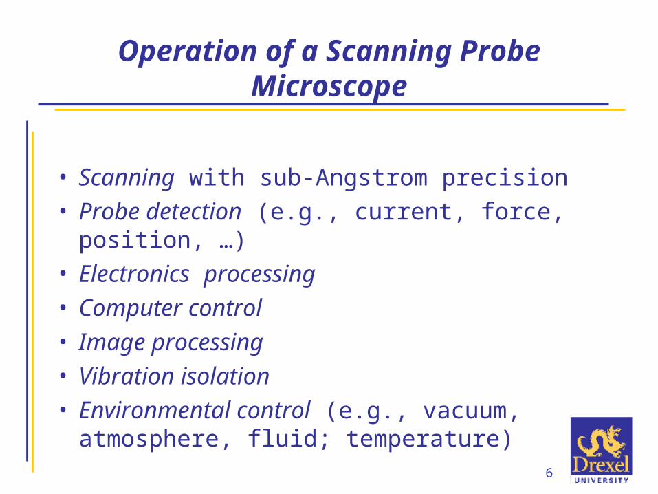
Operation of a Scanning Probe Microscope
• Scanning with sub-Angstrom precision• Probe detection (e.g., current, force, position, …)• Electronics processing• Computer control• Image processing• Vibration isolation• Environmental control (e.g., vacuum, atmosphere,
fluid; temperature)

7
Scanning Tunneling Microscope
Omicron

8
Scanning Force Microscope

9
Tunneling
• One-dimensional tunneling
• Density of electronic statesof sample and tip
2m1/ 2
2
I So 2
To 2
e 2d
So
= sample wavefunction
To
= tip wavefunction
= workfunction

10
Forces
non-contact Distance
tip to sample separation
repulsive force
attractive force
contact
Force
Trace
Retrace
F k x
Typical:
k 0.3N / m
x = 10nm
F = 3nN
Contact vs. non-contact modes ...Forces to atto-newton (10-18 N) range ...

11
Themes
• IMAGING
• INTERROGATING
• MANIPULATING
atoms and nanoscale objects
12
IMAGING
ATOMS AND NANOSCALE OBJECTSATOMS AND NANOSCALE OBJECTS

13
Large-scale Atomic-scale
Graphite4.2 nm 4.2 nm
STM
Gold Grating30 µm 30 µm
STMDiNardo

14
Semiconductor Surfaces - Si(100)
Tilted dimer
SymmetricDimer
Unreconstructed
L) OccupiedR) Unoccupied
Hamers, 1986

15
Temperature-dependent Reconstructions
• Low-temperature Si(100)-c(42) vs. (2 1)– Domain boundaries, p(2 2) regions
Wolkow, 1992

16
Homoepitaxial Growth - Si(100)
Mo, 1988

17
Fractional Images
• Probing atomic orbitals– Frequency-modulated
Atomic Force Microscopy
– Si tip / Si(111)-77
Si atom
Giessibl, 2000

18
Metal Surfaces
Wahlström, 1998

19
0.4 ML Ag/Cu(110)
c(102) model
a, b) 230230 nm2
c) 5.45.4 nm2
d) 3.83.8 nm2Sprunger, 1996

20
Interfaces - Cross-sectional Imaging
Ohmori, 1999

21
Molecular Adsorption - CO/Pt(111)
Pederson, 1996

22
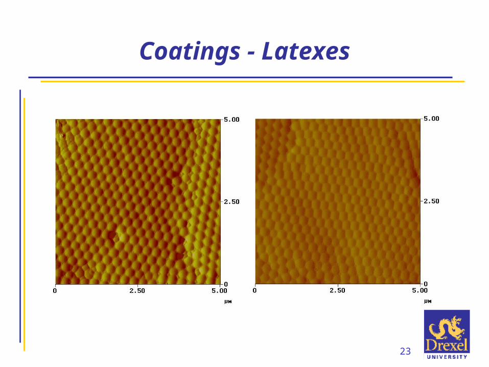
Coatings - Colloidal Latex Particles
VacancyRecoveryFaulted LayerInterstitial DefectLine DefectOrientation ChangeBrennan, 2000
23
Coatings - Latexes

24
Carbon Nanotubes
Odom, 1998
25
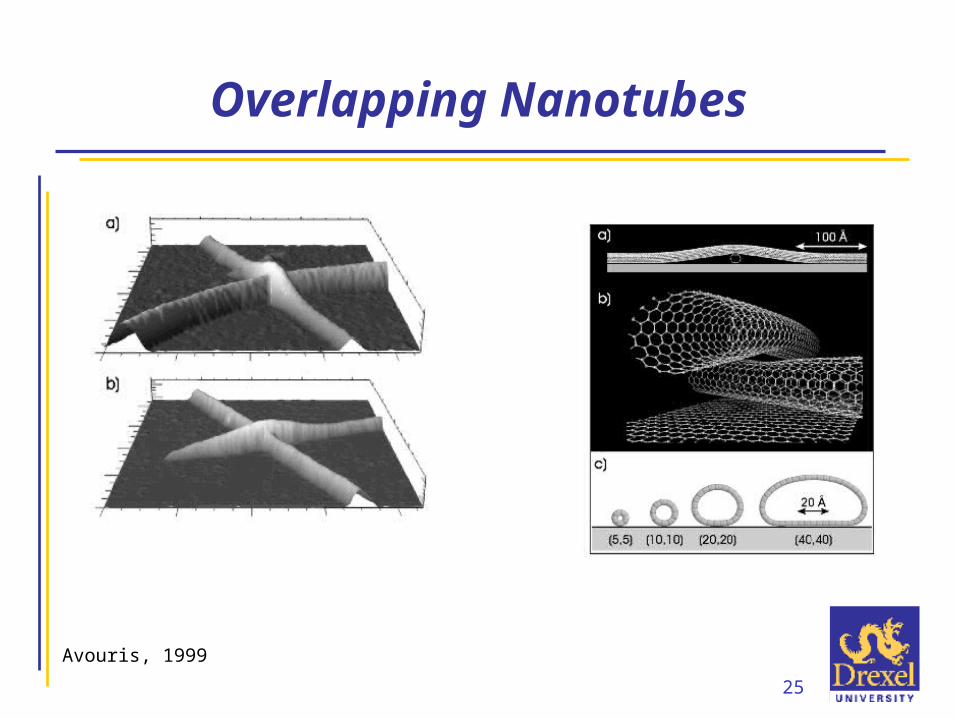
Overlapping Nanotubes
Avouris, 1999

26
Nanotube Shapes and Forces
Avouris, 1999
27
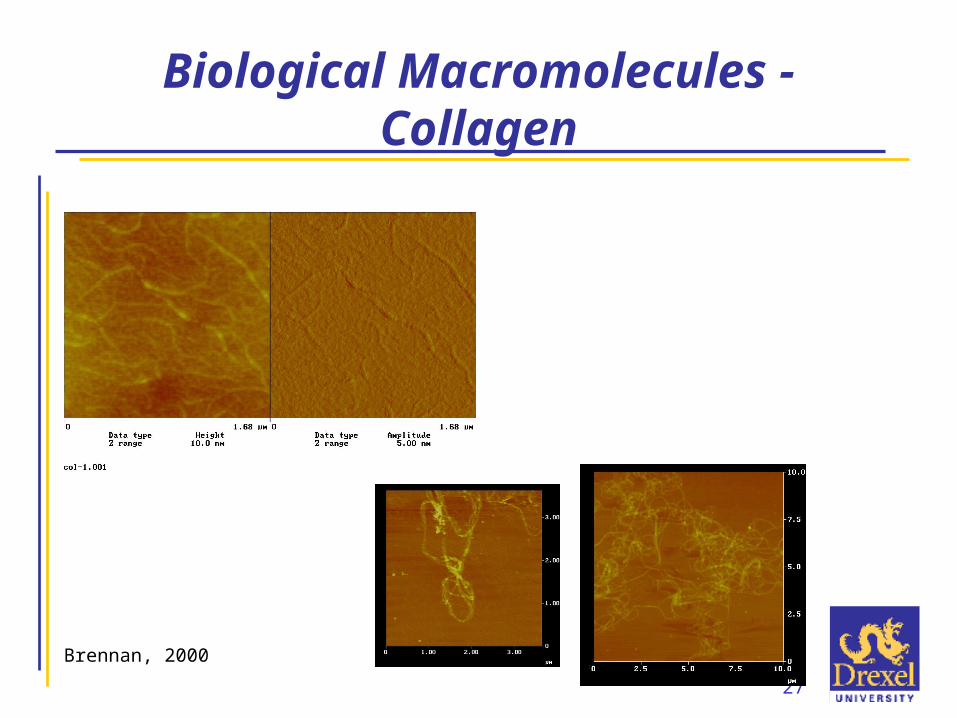
Biological Macromolecules - Collagen
Brennan, 2000

28
Biological Macromolecules - Fibronectin
Brennan, 1999

29
INTERROGATING
ATOMS AND NANOSCALE OBJECTSATOMS AND NANOSCALE OBJECTS
30
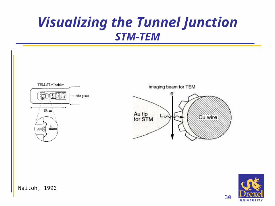
Visualizing the Tunnel JunctionSTM-TEM
Naitoh, 1996

31
Scanning
Ohnishi, 1998
32
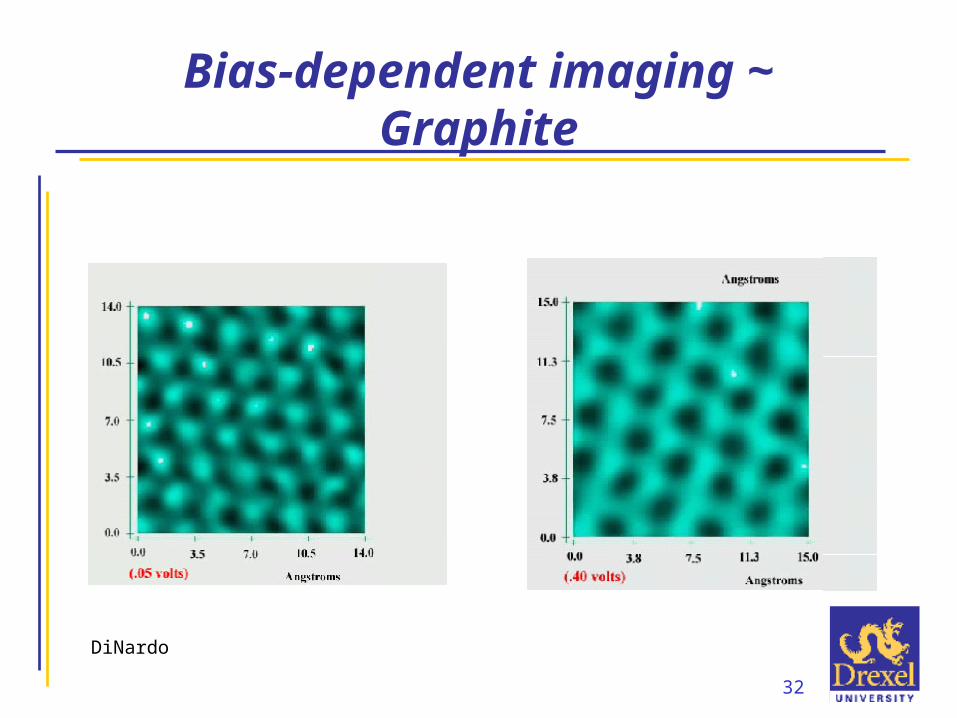
Bias-dependent imaging ~ Graphite
DiNardo

33
Bias-dependent imaging ~ GaAs(110)
• GaAs(110) (cleaved) surface
Feenstra, 1987

34
Spectroscopy ~ on the Nanoscale
• Beam techniques average over surface species• SPM techniques measure density of states related
to the atom (or molecule) under the tip– electronic spectrum - measure dI/dV [or (dI/dV)/(I/V)]
Hamers, 1986

35
Electronic SpectroscopyAtom by Atom
• Reconstructed Si(100)-21 surface– Dimers– Occupied electronic states of dimers (between atoms)
– Unoccupied electronic states of dimers (away from atoms)
Hamers, 1986

36
Defects
• Atomic-sized defects– Al/Si(111)-√3√3 structure
– different electronic states
Hamers, 1988
37
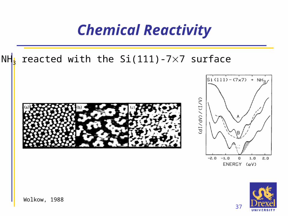
Chemical Reactivity
NH3 reacted with the Si(111)-77 surface
Wolkow, 1988

38
Vibrational SpectroscopyMolecule by Molecule
Lauhon, 2000

39
Chemical Reactions
Lauhon, 2000
Electron-induced dissociation product -pyridine on Cu(100) at 8K

40
Surface DiffusionChasing Atoms with the Atom Tracker
Swartzentruber, 1996
41
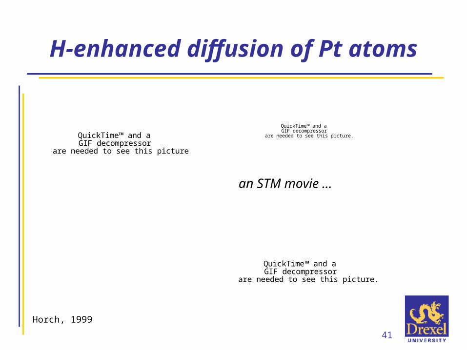
H-enhanced diffusion of Pt atoms
QuickTime™ and aGIF decompressor
are needed to see this picture.QuickTime™ and aGIF decompressor
are needed to see this picture.
QuickTime™ and aGIF decompressor
are needed to see this picture.
Horch, 1999
an STM movie ...

42
Electrostatic Force Microscopy (EFM)
• Application– Topography of integrated circuit
– Monitoring an active integrated circuit
Digital Instruments, www.di.com

43
Scanning Capacitance Microscopy
Nakakura, 1999

44
Magnetic Force Microscopy (MFM)
• Magnetic tip interaction with surface• Application: Disk drive
– Morphology
– Magnetic structure
Digital Instruments, www.di.com

45
Scanning Chemical Microscopy
• Measure chemical interaction between the tip and sample
• Functionalize the tip with hydrophobic or hydrophilic species
• Scan over surface and measure adhesion force or friction force

46
Carbon Nanotube Tips- Functionalization -
Wong, 1998

47
Scanning Chemical Microscopy
Frisbee, 1994 / Wong, 1998
48
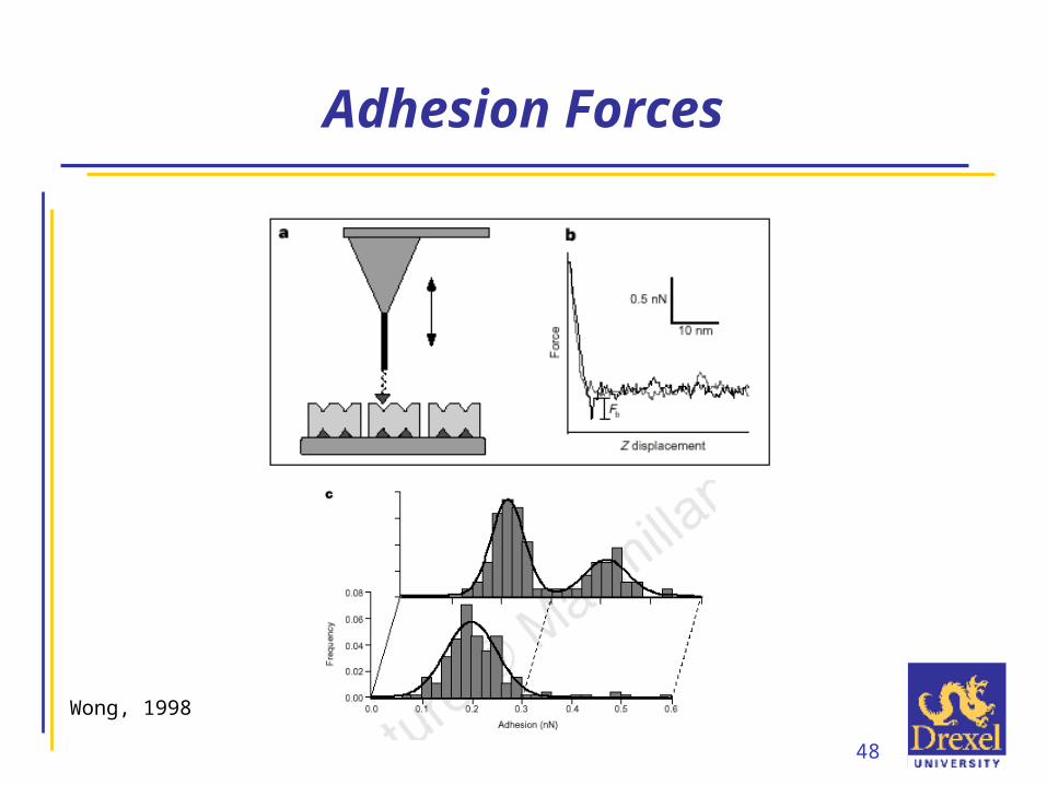
Adhesion Forces
Wong, 1998
49
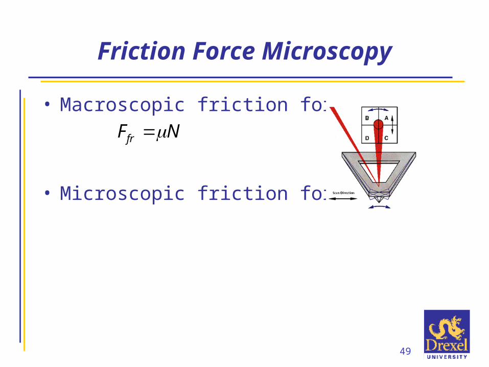
Friction Force Microscopy
• Macroscopic friction forces
• Microscopic friction forces
Ffr N

50
Polymer Thin Films
Nie, 1999
Polypropylene film(a) AFM + (b) FFM, (c) non-contact AFM

51
nN Bond ForcesStrength of a Covalent Bond
Grandbois, 1999
52
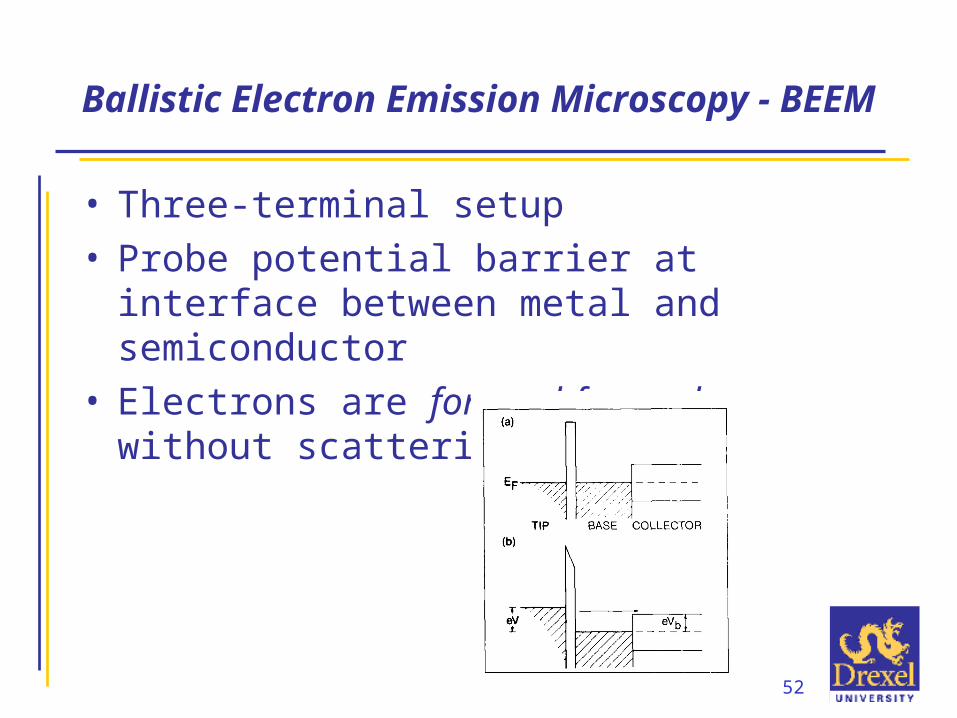
Ballistic Electron Emission Microscopy - BEEM
• Three-terminal setup• Probe potential barrier at interface between metal
and semiconductor• Electrons are forward-focused without scattering
(ballistic)

53
BEEM
Bell, 2000
54
MANIPULATING
ATOMS AND NANOSCALE OBJECTSATOMS AND NANOSCALE OBJECTS

55
Moving Atoms
• Xe– Physisorbed noble gas - (low temperature)
• Fe– Quantum “Corrals”
Eigler, 1991 / Crommie, 1993
56
Confined Electrons
• Reflections of free electron (waves) at boundaries
• Standing waves solutions
• One-dimensional free electron solution (infinite barrier)

57
Quantum Corral
Crommie, 1993

58
Forming Nanowires
Ohnishi, 1998

59
Nanowire modeling
Okamoto, 1999

60
Measuring Currents through One- and Two-atomic-row Nanowires
Ohnishi, 1998

61
Nanoelectronics
• Nanoscale channels
• Nanoscale objects
• Currents - description based on quantum-mechanical transport
62
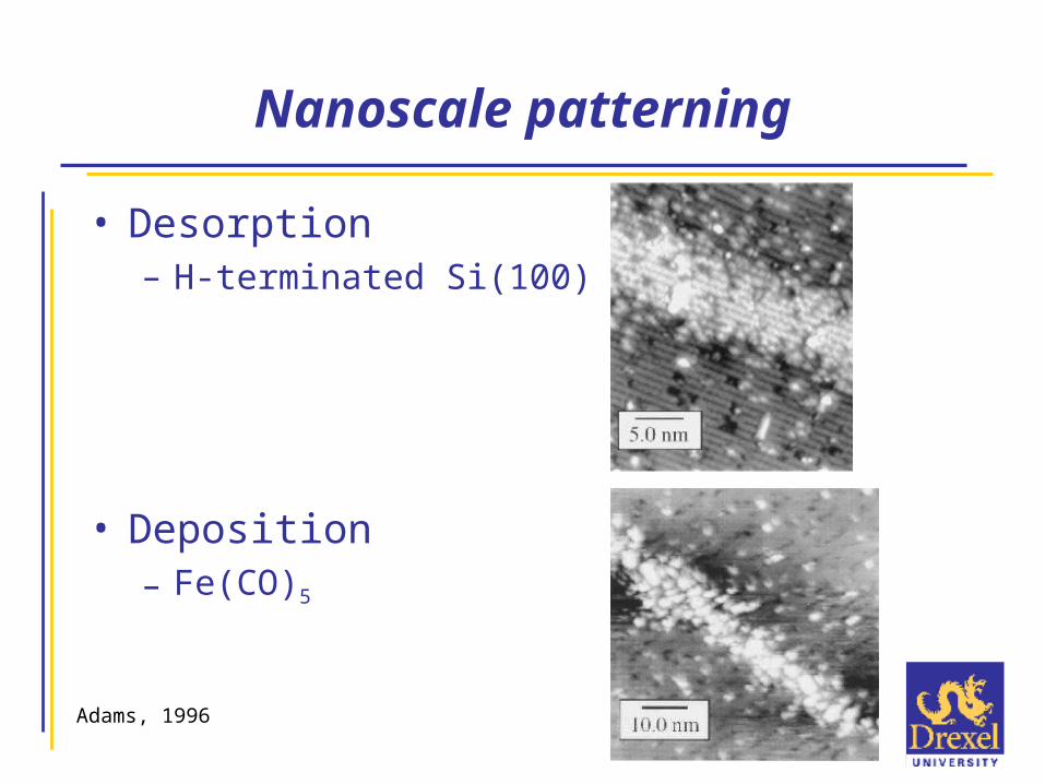
Nanoscale patterning
• Desorption– H-terminated Si(100)
• Deposition– Fe(CO)5
Adams, 1996
63
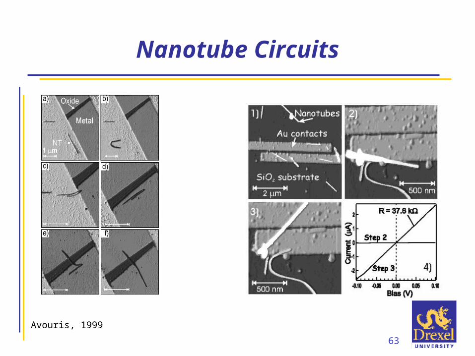
Nanotube Circuits
Avouris, 1999

64
Nanotube FET
Martel, 1998 / Avouris, 1999

65
Diamond-like Carbon Films
STM AFM
Mercer, 1996

66
Protein-folding Forces
Rief, 1999

67
Comparison of Force Curves
Rief, 1999

68
Related Techniques
• Scanning Near-field Optical Microscopy
• Scanning Thermal Microscopy

69
Some Acronyms ...
• STM• STS• AFM• TM-AFM• FFM, LFM• CFM