1 interconnect layout optimization by simultaneous steiner tree construction and buffer insertion...
TRANSCRIPT
1
Interconnect Layout Optimization by Simultaneous Steiner Tree Construction and
Buffer Insertion
Presented By Cesare Ferri
Takumi Okamoto , Jason Kong (ICCAD’96)

2
From the previous Lesson
Buffer insertion and Interconnect Topology optimizations have an important role for Timing optimizations of VLSI circuits.
Previous optimizations algorithms consider independently the 2 problems:the buffer insertion Steiner Tree construction (topology optimiz.)

3
Proposed Algorithm
The algorithm (BA-tree) addresses simultaneously the Steiner Tree construction problem and the Buffer insertion problem.
It makes use of two others algorithms: Heuristic A-tree Algorithm Van Ginneken algorithm (Buffer insertion)

4
Problem Formulation
Given:a source S0 and sinks
S1..Sn with given positions and RAT associated with each Si
Find:A Steiner tree Ts that
spans S and has buffers inserted
Objective : Maximized the RAT at the
source
Source
S0
sink1
sink2
sink3
sink4
RAT1
5
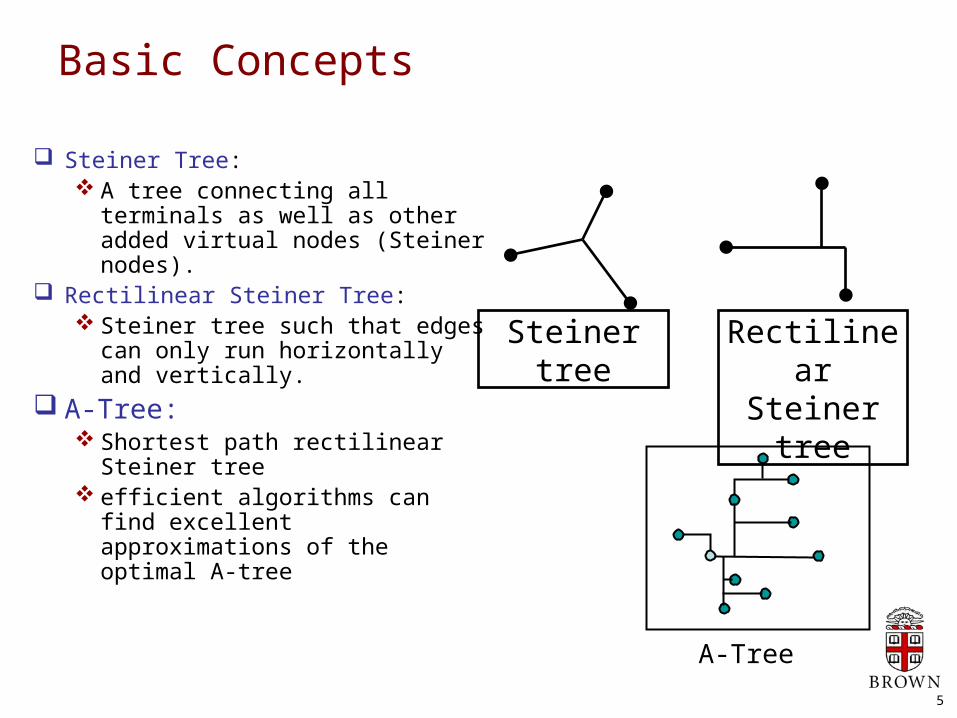
Basic Concepts
Steiner Tree: A tree connecting all terminals
as well as other added virtual nodes (Steiner nodes).
Rectilinear Steiner Tree: Steiner tree such that edges
can only run horizontally and vertically.
A-Tree: Shortest path rectilinear Steiner
tree efficient algorithms can find
excellent approximations of the optimal A-tree
Steiner tree
A-Tree
Rectilinear Steiner tree

6
Overall Algorithm
The algorithm consists of 2 phases:Bottom up tree construction (A-tree alg.)Top down buffer insertion (Van Ginneken
alg.)
The first phase recursively calls the A-tree algorithm
7
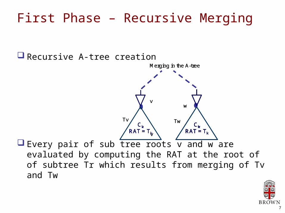
First Phase – Recursive Merging
Recursive A-tree creation
Every pair of sub tree roots v and w are evaluated by computing the RAT at the root of of subtree Tr which results from merging of Tv and Tw
v
Tv
w
Tw
Merging in the A-tree
Ck
RAT = Tk
Cv
RAT = Tv
Ck
RAT = Tk
Cw
RAT = T
v
Tv
w
Tw
Merging in the A-tree
Ck
RAT = Tk
Cv
RAT = Tv
Ck
RAT = Tk
Cw
RAT = TCk
RAT = Tk
Cw
RAT = T

8
Second Phase -
Top Down Buffer Insertion (Van Ginneken algorithm )The option that gives the Maximum Required
Arrival Time at root is chosenTraces back the computation of the first
phase that led this option

9
Experimental Results
Table: RAT at source (ns)
Sequential A-tree, Buffer insertion Proposed alg.
75% bigger RAT than the sequential alg
Net with # sinks
10
Conclusions
The BA-tree algorithm was presented, which derives buffered Steiner tree so that the RAT at the source is
Maximized achieves Steiner tree construction and buffer insertion
simultaneously
Experimental Results show that the algorithm increases the timing slack by up 75%
Future Work: Including the total capacitance minimization and their trade off
with the RAT at the source Incorporating optimal wiresizing for further delay optimizzation

11
optimal wire sizing and buffer insertion for low power
nuno alves
7 / december / 2006

12
what’s the paper about?
idea is simple: they want to improve delay while take power into account on VLSI circuits.
how can we improve delay & routability ?1. by sizing wires2. by inserting buffers
• sizing wires? yes! as we shrink down circuit size, wire becomes a contributor to to signal delay and time. by widening wires we reduce resistance, but we also increase capacitance
• inserting buffers?yes! read slides from previous class
13
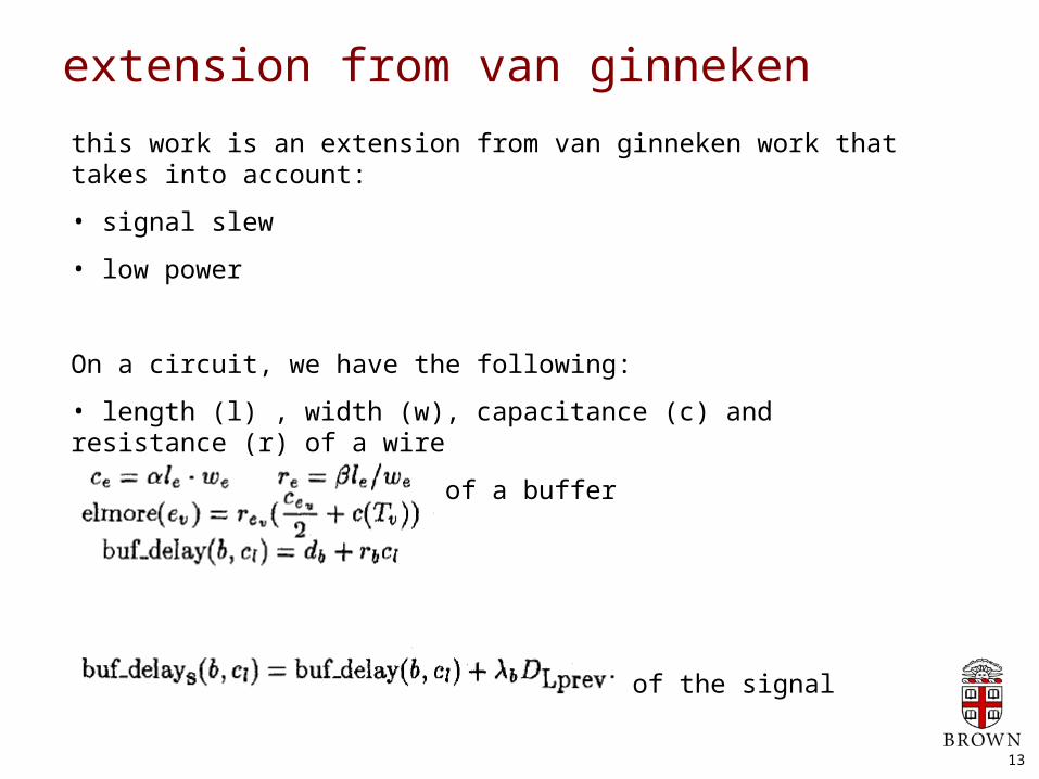
extension from van ginneken
this work is an extension from van ginneken work that takes into account:
• signal slew
• low power
On a circuit, we have the following:
• length (l) , width (w), capacitance (c) and resistance (r) of a wire
• capacitance and delay of a buffer
Model of buffer delay includes slew of the signal
14
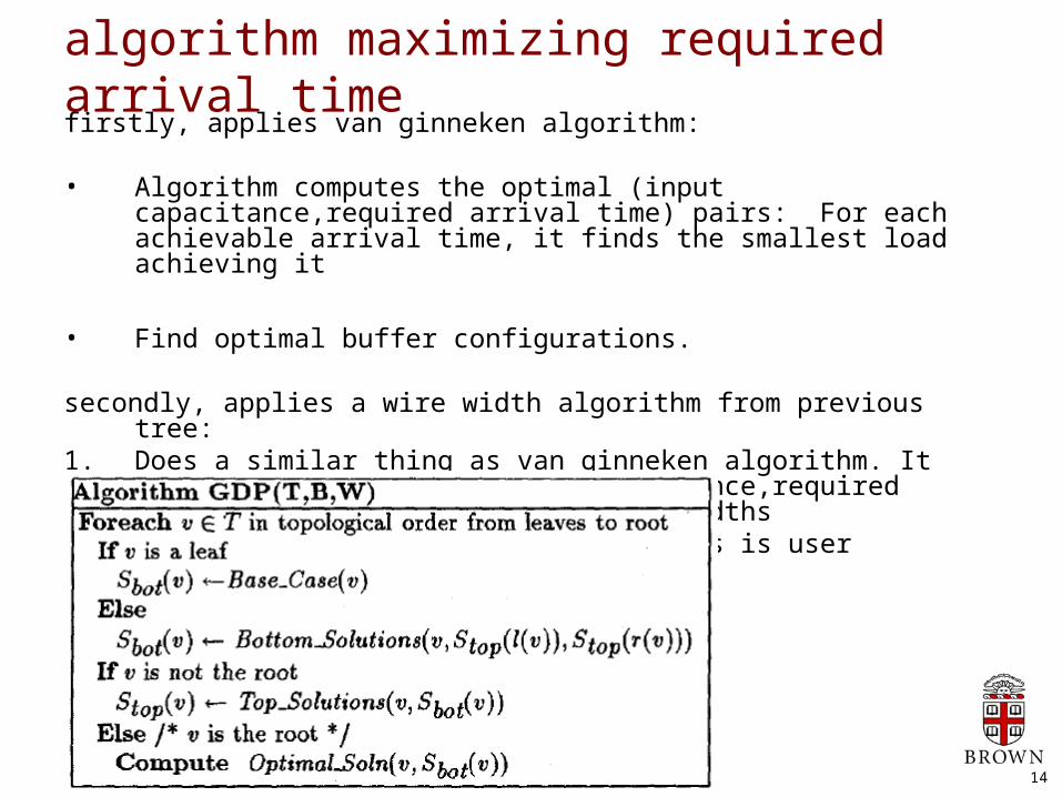
algorithm maximizing required arrival timefirstly, applies van ginneken algorithm:
• Algorithm computes the optimal (input capacitance,required arrival time) pairs: For each achievable arrival time, it finds the smallest load achieving it
• Find optimal buffer configurations.
secondly, applies a wire width algorithm from previous tree:1. Does a similar thing as van ginneken algorithm. It computes the optimal
(input capacitance,required arrival time) with different wire widths2. How much we can scale the wire widths is user specified
15
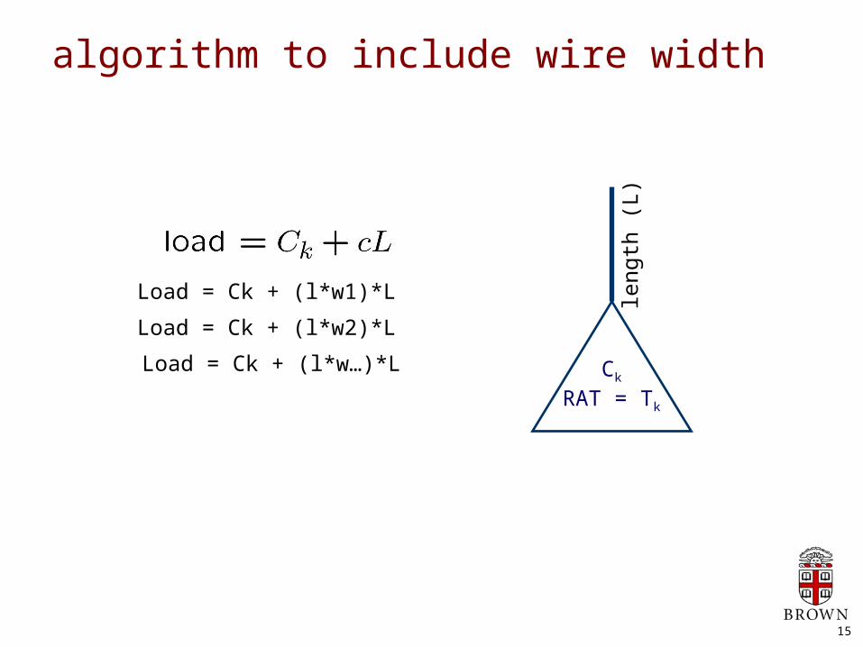
algorithm to include wire width
leng
th (
L)
Ck
RAT = Tk
Load = Ck + (l*w1)*L
Load = Ck + (l*w2)*L
Load = Ck + (l*w…)*L
16
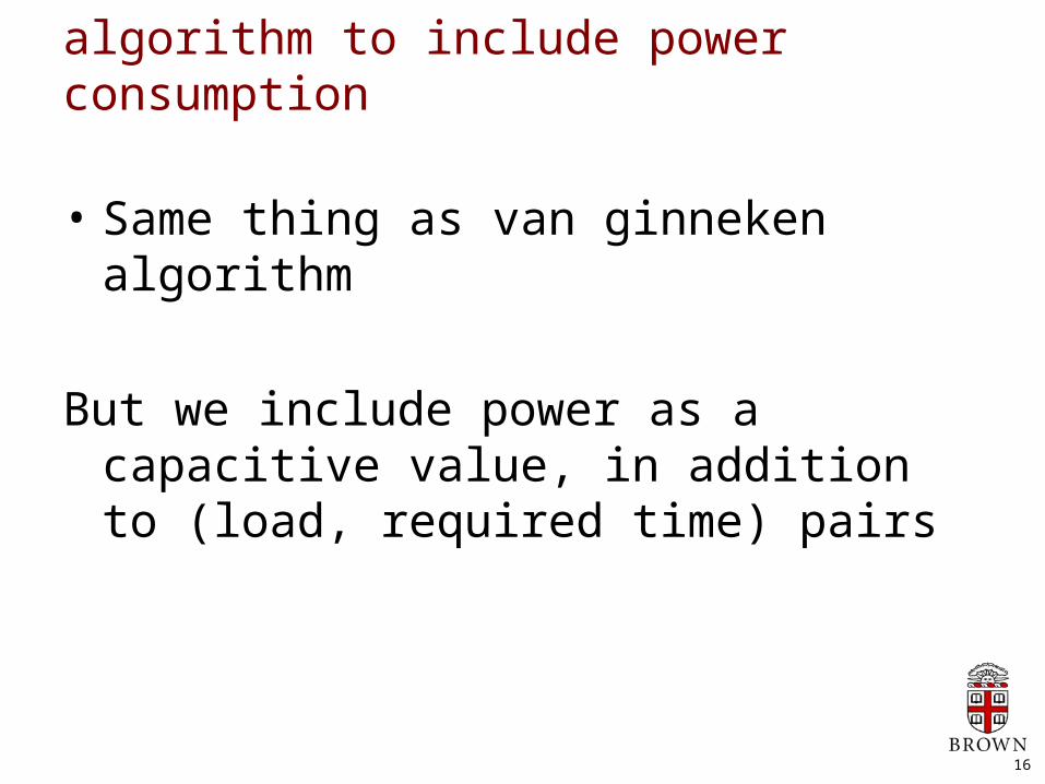
algorithm to include power consumption
• Same thing as van ginneken algorithm
But we include power as a capacitive value, in addition to (load, required time) pairs
17
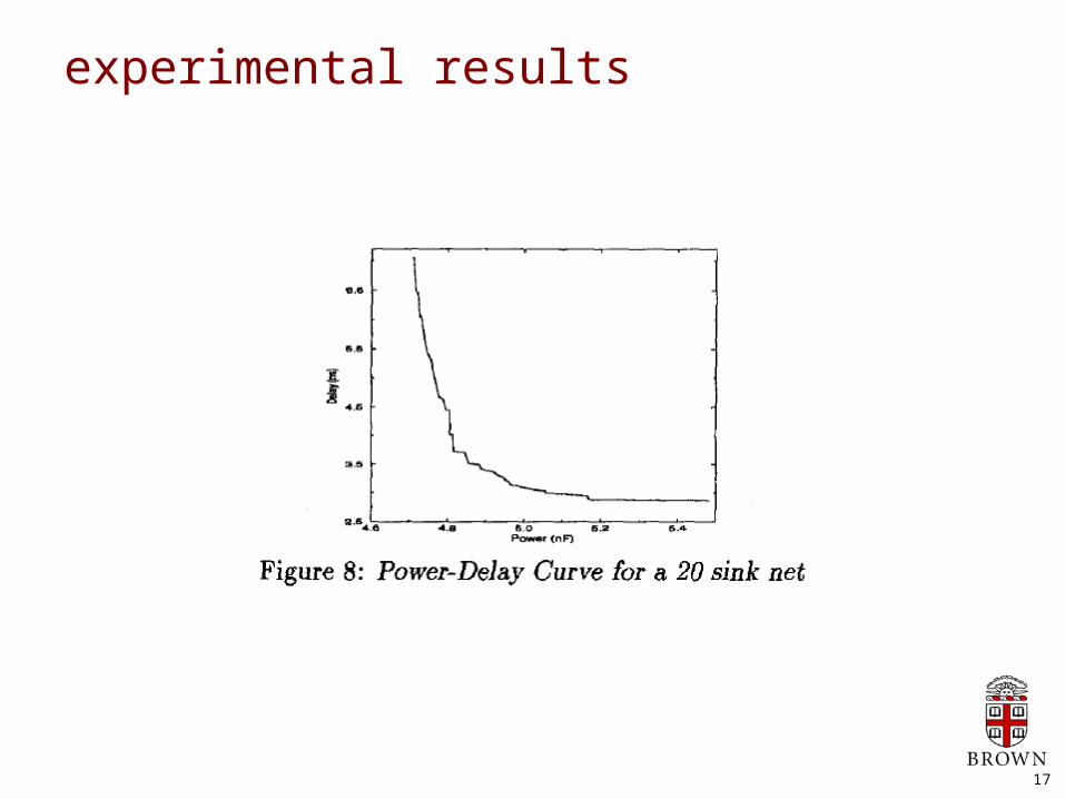
experimental results

18
Minimum-Buffered Routing of Non-Critical Nets
for Slew Rate and Reliability Control
C. Alpert, A. Kahng, B. Liu, I. Mandoiu, A. Zelikovsky
Presenter: Elif Alpaslan
19
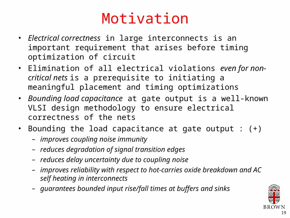
Motivation• Electrical correctness in large interconnects is an important
requirement that arises before timing optimization of circuit• Elimination of all electrical violations even for non-critical nets is a
prerequisite to initiating a meaningful placement and timing optimizations
• Bounding load capacitance at gate output is a well-known VLSI design methodology to ensure electrical correctness of the nets
• Bounding the load capacitance at gate output : (+)– improves coupling noise immunity
– reduces degradation of signal transition edges
– reduces delay uncertainty due to coupling noise
– improves reliability with respect to hot-carries oxide breakdown and AC self heating in interconnects
– guarantees bounded input rise/fall times at buffers and sinks
20
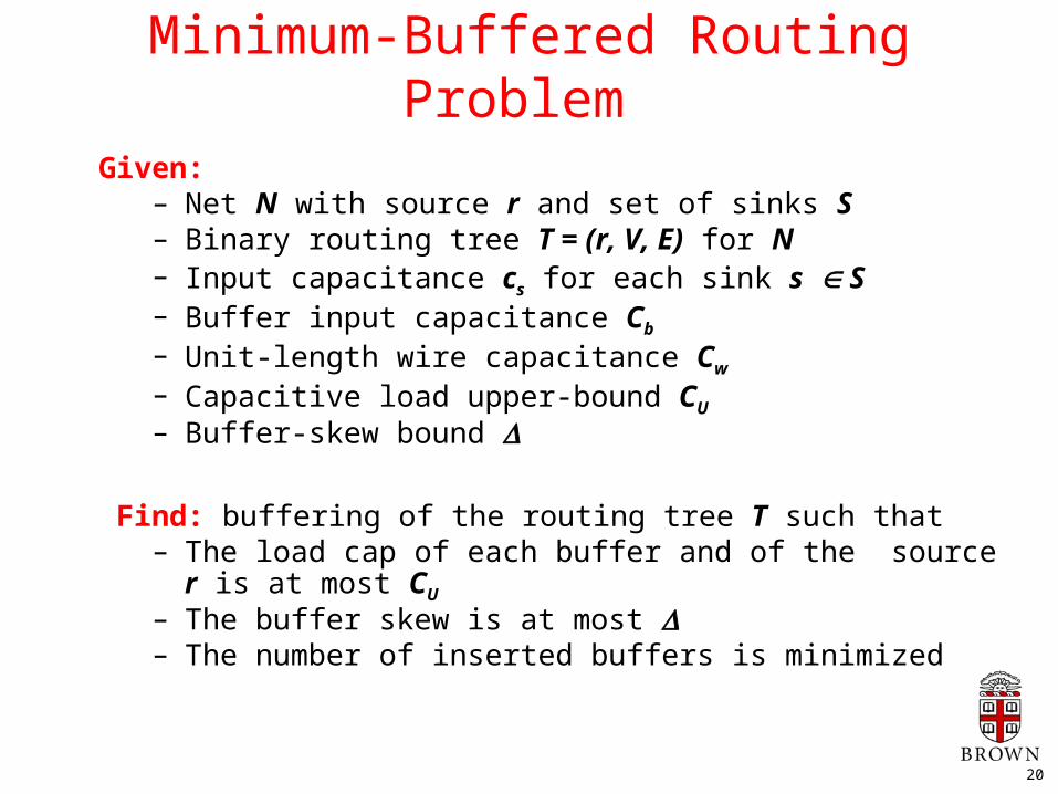
Minimum-Buffered Routing Problem Given:
– Net N with source r and set of sinks S– Binary routing tree T = (r, V, E) for N– Input capacitance cs for each sink s S– Buffer input capacitance Cb – Unit-length wire capacitance Cw
– Capacitive load upper-bound CU
– Buffer-skew bound
Find: buffering of the routing tree T such that– The load cap of each buffer and of the source r is at most CU
– The buffer skew is at most – The number of inserted buffers is minimized
21
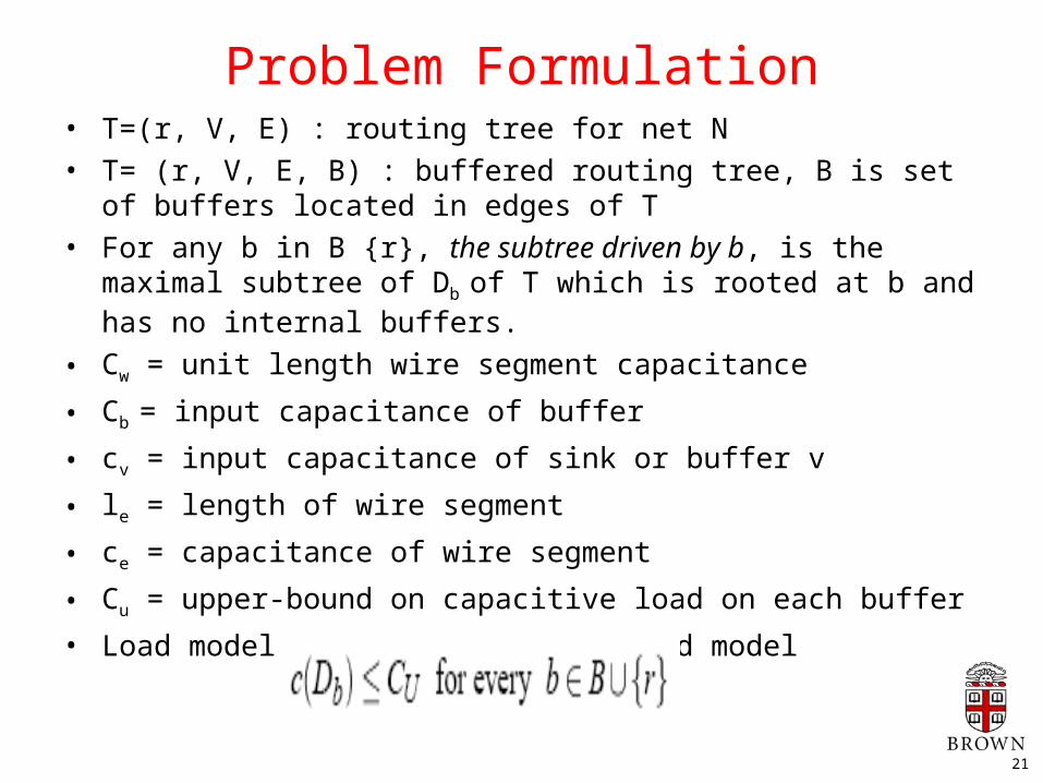
Problem Formulation• T=(r, V, E) : routing tree for net N• T= (r, V, E, B) : buffered routing tree, B is set of buffers located in
edges of T• For any b in B {r}, the subtree driven by b, is the maximal subtree of
Db of T which is rooted at b and has no internal buffers.
• Cw = unit length wire segment capacitance
• Cb = input capacitance of buffer
• cv = input capacitance of sink or buffer v
• le = length of wire segment
• ce = capacitance of wire segment
• Cu = upper-bound on capacitive load on each buffer
• Load model: lumped capacitive load model

22
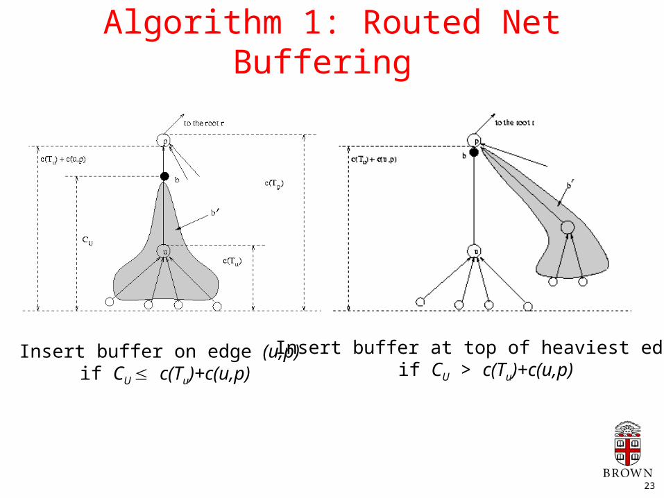
Algorithm 1: Routed Net Buffering • Linear Time Greedy Algorithm with a single non-inverting buffer
type
• Definitions used in the algorithm:
– Critical Vertex p: a vertex of a routing tree T is critical if p is a bottom-most point of T such that Tp can not be driven by a single buffer.
– Heaviest Child u of p: u is a heaviest child of p if it accumulates more capacitance than any other child of p.
23
Algorithm 1: Routed Net Buffering
Insert buffer on edge (u,p) if CU c(Tu)+c(u,p)
Insert buffer at top of heaviest edge if CU > c(Tu)+c(u,p)