1-w isolated power supply with planar transformer ...caxapa.ru/thumbs/851721/tidub83.pdf ·...
TRANSCRIPT

Voltage Inputs (V)
Effi
cien
cy
14 16 18 20 22 24 26 28 30 32 34 3660%
64%
68%
72%
76%
80%
D004
14 to 36 V
5 V40 mA
15 V30 mA
±15 V30 mA
LM5017Fly-Buck regulatorIntegrated FETs
TPS62175Buck regulator
Integrated FETs
TPS7A4901Ultralow NoisePositive LDO
TPS7A3001Ultralow NoiseNegative LDO
1TIDUB83–January 2016Submit Documentation Feedback
Copyright © 2016, Texas Instruments Incorporated
1-W Isolated Power Supply With Planar Transformer Reference Design
TI Designs1-W Isolated Power Supply With Planar TransformerReference Design
All trademarks are the property of their respective owners.
TI DesignsThe TIDA-00688 is an ultra-thin profile, 1-W outputisolated power supply. The design has a height of only2.2 mm on each side of the PCB and fits even in verysmall, space-constrained applications. The thin profileis achieved by using a planar transformer that isintegrated into the PCB. The TIDA-00688 has threeisolated outputs (15 V, –15 V, 5 V) and targets all kindof modules in the PLC, DCS, and PAC area that needa very thin and small, yet isolated, power supply.
Design Resources
TIDA-00688 Design FolderTIDA-00237 Tools FolderTIDA-00129 Tools FolderLM5017 Product FolderTPS62175 Product FolderTPS7A4901 Product FolderTPS7A3001 Product Folder
ASK Our E2E Experts
Design Features• Integrated Planar Transformer• Wide Input Voltage Range: 14 to 36 V (24 VNOM)• Three Isolated Outputs:
– 15 VISO, 30 mA Ultralow Noise– –15 VISO 30 mA Ultralow-Noise– 5 VISO, 40 mA
• Ultrathin Profile Of Only 2.2 mm
Featured Applications• PLC, DCS, and PAC:
– Analog Input Module– Analog Output Module– Transducer Module– Special Function Module

Key System Specifications www.ti.com
2 TIDUB83–January 2016Submit Documentation Feedback
Copyright © 2016, Texas Instruments Incorporated
1-W Isolated Power Supply With Planar Transformer Reference Design
An IMPORTANT NOTICE at the end of this TI reference design addresses authorized use, intellectual property matters and otherimportant disclaimers and information.
1 Key System Specifications
Table 1. Key System Specifications
SYMBOL PARAMETER CONDITIONSSPECIFICATION
UNITMIN TYP MAX
VIN Input voltage Normal operation 14 24 36 VIQ Quiescent current No output load — 9 15 mAVJ2 Output voltage connector J2 Normal operation 4.9 5 5.1 VVJ3 Output voltage connector J3 Normal operation 14.8 15 15.2 VVJ4 Output voltage connector J4 Normal operation –14.8 –15 –15.2 VIJ2 Output current VIN > VIN(min) 0 — 40 mAIJ3 Output current VIN > VIN(min) 0 — 30 mAIJ4 Output current VIN > VIN(min) 0 — 30 mA
POUT Output power 0 — 1.1 W
h EfficiencyVIN = 14 V, IOUT,GES = 106 mA — 76.9 — %VIN = 24 V, IOUT,GES = 10 mA — 73.3 — %VIN = 36 V, IOUT,GES = 106 mA — 52.6 — %
H1 Component height abovePCB — — 2.2 mm
H2 Component height belowPCB — — 2.2 mm
AA Active area size — — 25.4 × 43.8 mm2
14 to 36 V
5 V40 mA
15 V30 mA
±15 V30 mA
LM5017Fly-Buck regulatorIntegrated FETs
TPS62175Buck regulator
Integrated FETs
TPS7A4901Ultralow NoisePositive LDO
TPS7A3001Ultralow NoiseNegative LDO
PGA
REF
ADC
Protection and filter
Protection and filter
Protection and filter
Protection
RTD ref voltage
RTD excitation
MUX
Integrated front-end
Dataisolation
SPI
33
11
www.ti.com System Description
3TIDUB83–January 2016Submit Documentation Feedback
Copyright © 2016, Texas Instruments Incorporated
1-W Isolated Power Supply With Planar Transformer Reference Design
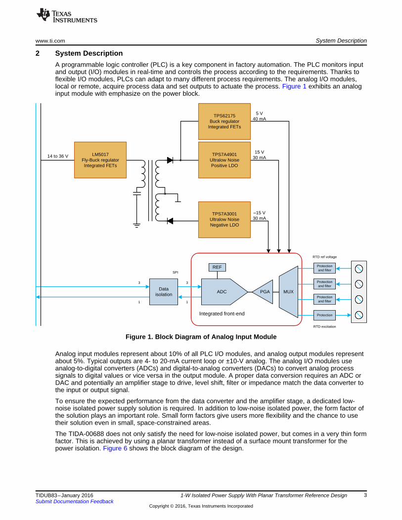
2 System DescriptionA programmable logic controller (PLC) is a key component in factory automation. The PLC monitors inputand output (I/O) modules in real-time and controls the process according to the requirements. Thanks toflexible I/O modules, PLCs can adapt to many different process requirements. The analog I/O modules,local or remote, acquire process data and set outputs to actuate the process. Figure 1 exhibits an analoginput module with emphasize on the power block.
Figure 1. Block Diagram of Analog Input Module
Analog input modules represent about 10% of all PLC I/O modules, and analog output modules representabout 5%. Typical outputs are 4- to 20-mA current loop or ±10-V analog. The analog I/O modules useanalog-to-digital converters (ADCs) and digital-to-analog converters (DACs) to convert analog processsignals to digital values or vice versa in the output module. A proper data conversion requires an ADC orDAC and potentially an amplifier stage to drive, level shift, filter or impedance match the data converter tothe input or output signal.
To ensure the expected performance from the data converter and the amplifier stage, a dedicated low-noise isolated power supply solution is required. In addition to low-noise isolated power, the form factor ofthe solution plays an important role. Small form factors give users more flexibility and the chance to usetheir solution even in small, space-constrained areas.
The TIDA-00688 does not only satisfy the need for low-noise isolated power, but comes in a very thin formfactor. This is achieved by using a planar transformer instead of a surface mount transformer for thepower isolation. Figure 6 shows the block diagram of the design.

FB
VINVCC
SW
RTN
BST
1.225V
VILIM
LM5017
RON
ILIMCOMPARATOR
+
-
V UVLO
ON/OFF
TIMERS
COT CONTROL
LOGIC
1.225V
START-UP
REGULATOR
VIN
FEEDBACK
DISABLE
THERMAL
SHUTDOWN
UVLO
OVER-VOLTAGE1.62V
UVLO
4.5V
SD
SHUTDOWN
VDD REG
BG REF
0.66V
20 µA
CURRENT
LIMIT
ONE-SHOT
System Design Theory www.ti.com
4 TIDUB83–January 2016Submit Documentation Feedback
Copyright © 2016, Texas Instruments Incorporated
1-W Isolated Power Supply With Planar Transformer Reference Design
3 System Design TheoryFor a 1-W isolated power supply with a wide input voltage range, no optocoupler feedback, and lownumber of external components, the Fly-Buck™ topology is superior to a flyback design. This topologyalso allows design flexibility for a primary non-isolated power supply. For a high-end post regulation, LDOswith high PSRR ensure a clean power supply for analog circuits. The 5-V rail is derived from the 18-Vtransformer output using a high efficiency buck regulator. The Fly-Buck is implemented using an LM5017.This part fulfils the Fly-Buck requirements while allowing a small circuit footprint at a low BOM cost.Figure 2 shows the architecture of the LM5017.
Figure 2. LM5017 Architecture
The TIDA-00688 is based on the TIDA-00237 but reduces height further down to 2.2 mm (1.6-mm PCBthickness) on each PCB side. This is achieved by replacing the surface mount transformer with a planartransformer. The magnetic core of a planar transformer consists out of two parts. First, an E-shaped ferrite(E-core) is put into three holes inside the PCB. Then, a planar ferrite is put from the other side onto thelegs of the E-core and fixed to it. In a planar transformer, the windings are placed in the same layer andwired around the middle leg of the magnetic core like a spiral. To increase the inductance of those coils, itis possible to use several layers. However, to keep PCB manufacturing cost down, the TIDA-00688 onlyuses a four-layer design: one primary side layer, two secondary side layers, and one interconnectionlayer. The design process of the transformer is explained further in Section 3.2.

C1
C1
IN
IN
VD
V
V D V 0.5 14 V 7 V
=
® = ´ = ´ =
www.ti.com System Design Theory
5TIDUB83–January 2016Submit Documentation Feedback
Copyright © 2016, Texas Instruments Incorporated
1-W Isolated Power Supply With Planar Transformer Reference Design
3.1 Primary-Side Output Voltage VC1
The primary-side voltage VC1 depends on multiple factors. As a rule of thumb, the duty cycle should bebelow 50%. Otherwise, the transfer time for the energy required to maintain the minimum secondaryvoltage at maximum current is too short. Short energy transfer times lead to larger peak currents, inferiorload regulation performance, and larger voltage drops across the rectifier diodes D2 and D3 on thesecondary side as well as across the synchronous rectifier inside the LM5017.
The TIDA-00688 is rated for an input voltage range of 14 to 36 V. According to Equation 1, a maximumduty cycle D of 50% corresponds to a primary side voltage VC1 of 7 V.
(1)
For an output voltage of 18 V on the secondary side, a turn ratio of 1:2.6 is needed. However, a turn ratioof 1:2.6 leads to high peak currents in the MOSFETs of the LM5017. Instead, with a turn ratio of 1:2, it ispossible to keep the peak currents below the specified limits of the LM5017. In conclusion, VC1 isregulated to 9 V, which results in a maximum duty cycle of 62%. At this duty cycle, the design is stillworking stable.
The LM5017 uses a constant on-time (COT) control scheme to control its switching behavior. The COTworks as follows. The on time is controlled by an on timer. The off time is defined by the time the feedbackvoltage drops below the reference voltage. This means the off time is terminated when the lower end ofthe output ripple voltage matches the reference voltage of the LM5017.
Note that the voltage ripple at C1 is highest for lowest input voltages. This is because the duty cycle isalso higher for lower input voltages, as shown in Equation 1. A longer duty cycle means that the high-sideFET of the LM5017 is turned on longer, too. As a result, the voltage ripple at C1 is higher, too. However,the average voltage across C1 is lower for lower input voltages.
3.2 Transformer DesignFor the transformer design, several things need to be considered: size and space constraints on the PCB,the operating frequency of the LM5017, the maximum allowable magnetic flux inside the magnetic core,the current ripple, DC losses of the PCB coils, and general DC losses occurring in every part.
Table 2 shows the calculation of the minimum primary side voltage of the transformer. Some margin isrequired for load regulation and general DC losses on top of the minimum required voltage of 8.7 V at C1.In conclusion, setting the primary side voltage to 9 V is sufficient and complies well with the considerationin Section 3.1.
Table 2. Primary-Side Voltage Calculation
PARAMETER CONDITION VALUEVJ3/J4 Full load 15.000 VLDO (U2, U3) drop-out voltage 30 mA, 125°C 0.180 VDiode D2 and D3 drop-out voltage 260 mA (average forward current) 0.550 VTransformer T1, secondary winding loss 1.46 Ω, 260 mA (average forward current) 0.380 VRequired transformer T1, secondary winding voltage 16.110 VRequired transformer T1, primary voltage Winding ration 1:2 8.055 VTransformer T1, primary winding loss 0.282 Ω, 500 mA (average forward current) 0.141 VU1 synchronous switch loss 1 Ω, 500 mA (average forward current) 0.500 VRequired voltage at C1 8.696 VVIN,MIN duty cycle VIN = 14 V 62.11%VIN,MAX duty cycle VMAX = 36 V 24.16%
H (A/m)
B (
mT
)
-1000 -750 -500 -250 0 250 500 750 1000-500
-250
0
250
500
D001
25°C100°C
H (A/m)
B (
mT
)
-10 -8 -6 -4 -2 0 2 4 6 8 10-300
-200
-100
0
100
200
300
D002
25°C100°C
( )
( )
1on,max
tr on,max pr,min 2
e
9 Vt 200 kHz 1.25 s
36 V
V t 36 V 9 V 1.25 sN 5.73
A B 39.3 mm 150 mT
-= ´ = m
´ - ´ m= = =
´ D ´
System Design Theory www.ti.com
6 TIDUB83–January 2016Submit Documentation Feedback
Copyright © 2016, Texas Instruments Incorporated
1-W Isolated Power Supply With Planar Transformer Reference Design
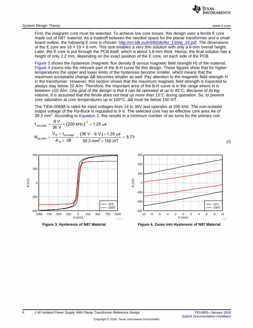
First, the magnetic core must be selected. To achieve low core losses, this design uses a ferrite E coremade out of N87 material. As a tradeoff between the needed space for the planar transformer and a smallboard outline, the following E core is chosen: http://en.tdk.eu/inf/80/db/fer_13/elp_18.pdf. The dimensionsof the E core are 18 × 10 × 6 mm. This size enables a very thin solution with only a 6-mm overall height.Later, the E core is put through the PCB itself, which is about 1.6-mm thick. Hence, the final solution has aheight of only 2.2 mm, depending on the exact position of the E core, on each side of the PCB.
Figure 3 shows the hysteresis (magnetic flux density B versus magnetic field strength H) of the material.Figure 4 zooms into the relevant part of the B-H curve for this design. These figures show that for highertemperatures the upper and lower limits of the hysteresis become smaller, which means that themaximum acceptable change ΔB becomes smaller as well. Pay attention to the magnetic field strength Hin the transformer. However, this section shows that the maximum magnetic field strength is expected toalways stay below 10 A/m. Therefore, the important area of the B-H curve is in the range where H isbetween ±10 A/m. One goal of the design is that it can be operated at up to 85°C. Because of its bigvolume, it is assumed that the ferrite does not heat up more than 15°C during operation. So, to preventcore saturation at core temperatures up to 100°C, ΔB must be below 150 mT.
The TIDA-00688 is rated for input voltages from 14 to 36V and operates at 200 kHz. The non-isolatedoutput voltage of the Fly-Buck is regulated to 9 V. The selected core has an effective core area Ae of39.3 mm2. According to Equation 2, this results in a minimum number of six turns for the primary coil.
(2)
Figure 3. Hysteresis of N87 Material Figure 4. Zoom into Hysteresis of N87 Material

3076 200 mA
N I A2H 4.14
l 0.29 m m
æ ö´ +ç ÷´ è ø= = =
IN IN OUT OUT
OUT OUT
IN
IN
V I V I
V I 18 V 70 mA 18 V 30 mAI 200 mA
V 9V
´ = ´
´ ´ + - ´
® = = =
( )pr on,max
pr
V t 36 V 9 V 1.25 sI 307 mA
L 110 H
´ - ´ mD = = =
m
8
Cu
l 0.29 mR 1.7 10 282 m
A 0.035 mm 0.5 mm
m
-= r ´ = ´ W ´ = W
´
8Cu
7Cu o
m2 2 1.7 100.147 mm
H2 f2 200 kHz 1 4 10
m
-
-
r ´ ´ Wd = = =
p m mp ´ ´ ´ p ´
www.ti.com System Design Theory
7TIDUB83–January 2016Submit Documentation Feedback
Copyright © 2016, Texas Instruments Incorporated
1-W Isolated Power Supply With Planar Transformer Reference Design
3.2.1 Primary CoilStandard PCB fabrication requires a minimum distance of 0.15 mm between two traces. For betterisolation, leave some distance between the trace and the magnetic core. Furthermore, at one side of thecoil, vias are needed to route from the inside to the outside of the coil. These vias are placed 2 mm awayfrom the magnetic core.
To keep these distances and also to keep the DC resistance of the coil as low as possible a trace width of0.5 mm is chosen. This leaves a distance of around 0.62 mm between the outer or inner winding and themagnetic core. The resulting coil has a length of 0.29 m and an inductance of 110 μH.
Equation 3 calculates the skin depth δ for a defined frequency. At an operating frequency of 200 kHz, theskin depth is 0.146 mm. Because the thickness of the PCB trace is only 0.035 mm, the skin effect can beneglected.
(3)
The DC resistance of the coil can be calculated with Equation 4.
(4)
The resulting current ripple is calculated to 307 mA using Equation 5.
(5)
To estimate the DC current on the primary side under full load condition, assume the following inputs,slightly higher voltage outputs, and a perfect transformer with no losses:Output 1: 18 V, 30 mA + 40 mAOutput 2: -18 V, 30 mA
(6)
With the calculated DC current on the primary side, the length of the coil, and Equation 7, the maximummagnetic field strength H is calculated to 4.14 A/m.
(7)
Taking into account the ripple of around 307 mA, the maximum magnetic field strength is calculated to7.31 A/m. Therefore, assume that the maximum magnetic field strength always stays below ±10 A/m.

System Design Theory www.ti.com
8 TIDUB83–January 2016Submit Documentation Feedback
Copyright © 2016, Texas Instruments Incorporated
1-W Isolated Power Supply With Planar Transformer Reference Design
3.2.2 Secondary CoilTo get to the desired output voltage of ±18 V on the secondary side, two coils each with a winding ratio ofabout 1:2, compared to the primary coil, are needed. Therefore, the coils need 12 windings each. Groundpotential of the secondary side is set at the connection point between the two coils. Figure 5 shows thelayer setup of the secondary side.
Figure 5. Secondary Side Setup (Secondary Coil 1, Secondary GND (Lower Part), Secondary Coil 2)
Again, to stay within standard fabrication limits and to find a good trade-off between trace width and DCresistance, a trace width of 0.2 mm and a distance of 0.15 mm between the traces are selected. Thisleaves a distance of around 0.475 mm between the outer and inner winding and the magnetic core. Likefor the primary coil, necessary vias for routing are placed 2 mm away from the magnetic core.
The resulting secondary coils have a length of 0.6 m each. As before, the skin effect can be neglected.Again, using Equation 4 the DC resistance of each secondary coil is calculated to 1.46 Ω.
C1
SW 10
10
Vf
10 R4
9 VR4 450 k
10 200 kHz
-
-
=
´
= = W
´
www.ti.com System Design Theory
9TIDUB83–January 2016Submit Documentation Feedback
Copyright © 2016, Texas Instruments Incorporated
1-W Isolated Power Supply With Planar Transformer Reference Design
3.3 Operating Switching FrequencyAn operating frequency of 200 kHz is chosen. This frequency enables to stay within the limits for ΔB andsets an acceptable current ripple. Furthermore, this frequency complies with the operatingrecommendation of the selected magnetic core.
The selected frequency sets the minimum energy transfer time for the transformer to 1.25 μs. Theswitching frequency is set with resistor R4.
(8)
The next closest standard resistor value is 453 kΩ.
3.4 Output Ripple ConfigurationAs mentioned in Section 3.1, the LM5017 uses a COT control scheme where the on-time is controlled witha timer. The off-time is terminated when the feedback voltage falls below the reference voltage. For stableoperation, it is necessary that during off time the feedback voltage decreases monotonically in phase withthe inductor current. To ensure the correct ripple injection in the regulation loop, three different schemesare possible. This design follows scheme type 3 of AN-2292 Designing an Isolated Buck (Fly-Buck)Converter [3] with some modifications required to support the large input voltage range and low inputvoltage.

14 to 36 V
5 V40 mA
15 V30 mA
±15 V30 mA
LM5017Fly-Buck regulatorIntegrated FETs
TPS62175Buck regulator
Integrated FETs
TPS7A4901Ultralow NoisePositive LDO
TPS7A3001Ultralow NoiseNegative LDO
Block Diagram www.ti.com
10 TIDUB83–January 2016Submit Documentation Feedback
Copyright © 2016, Texas Instruments Incorporated
1-W Isolated Power Supply With Planar Transformer Reference Design
4 Block Diagram
Figure 6. TIDA-00688 Block Diagram
4.1 Highlighted ProductsThe TIDA-00688 provides isolated analog and digital supply voltages for PLC analog I/O modules. For theanalog section of the modules, the TIDA-00688 generates ±15 V. These output voltages are highlyaccurate and have minimal noise. The additional 5-V supply can be used as digital components like dataconverters, microcontrollers, or other isolated devices. To avoid the need for a third transformer secondarywinding, this voltage is created from the 15-V rail using a high efficiency DC/DC converter.
4.1.1 LM5017The LM5017 is a 100-V, 600-mA synchronous step-down regulator with integrated high-side and low-sideMOSFETs. The COT control scheme employed in the LM5017 requires no loop compensation, providesexcellent transient response, and enables very high step-down ratios. The on-time varies inversely withthe input voltage resulting in nearly constant frequency over the input voltage range. A high-voltagestartup regulator provides bias power for internal operation of the IC and for integrated gate drivers. Apeak current limit circuit protects against overload conditions. The under voltage lockout (UVLO) circuitallows the input under voltage threshold and hysteresis to be independently programmed. Other protectionfeatures include thermal shutdown and bias supply undervoltage lockout (VCC UVLO).
4.1.2 TPS7A4901The TPS7A4901 is a positive, high-voltage (36 V), ultralow-noise (15.4 μVRMS, 72-dB PSRR) linearregulator capable of sourcing a load of 150 mA. This linear regulator includes a capacitor-programmablesoft-start function that allows for delaying the output voltage generation until the power source is operatingstable. Other features available include built-in current limit and thermal shutdown protection to safeguardthe device and system during fault conditions. The TPS7A4901 is designed using bipolar technology andis ideal for high-accuracy, high-precision instrumentation applications where clean voltage rails are criticalto maximize system performance. This design makes the device an excellent choice to power operationalamplifiers, ADCs, DACs, and other high-performance analog circuitry. In addition, the TPS7A4901 issuitable for post DC/DC converter regulation. By filtering out the output voltage ripple inherent to DC/DCswitching conversion, maximum system performance is provided in sensitive instrumentation, test andmeasurement, audio, and RF applications.
www.ti.com Getting Started Hardware
11TIDUB83–January 2016Submit Documentation Feedback
Copyright © 2016, Texas Instruments Incorporated
1-W Isolated Power Supply With Planar Transformer Reference Design
4.1.3 TPS7A3001The TPS7A3001 complements the TPS7A4901 described in Section 4.1.2. It is a negative, high-voltage(–36 V), ultralow-noise (15.1 μVRMS, 72-dB PSRR) linear regulator capable of sourcing a maximum load of200 mA. The feature list of the TPS3001 is a 1:1 equivalent to the one of the TPS7A4901.
4.1.4 TPS62175The TPS62175 is a high-efficiency synchronous step-down DC-DC converter, based on the DCS-Controltopology, with a wide operating range of input voltage from 4.75 to 28 V providing up to a 500-mA outputcurrent. The TPS62175 automatically enters a power save mode at light loads, to maintain high efficiencyacross the whole load range. As well, it features a sleep mode to supply applications with advanced powersave modes like ultralow-power microcontrollers. The Power Good output may be used for powersequencing or power-on reset. The device features a typical quiescent current of 22 μA in normal modeand 4.8 μA in sleep mode. In sleep mode, the efficiency at very low load currents can be increased by asmuch as 20%. In shutdown mode, the shutdown current is less than 2 μA and the output is activelydischarged.
5 Getting Started HardwareThe design can be operated out of the box. Load resistors with a power rating of at least 500 mW can beconnected directly to the output terminals. To perform a maximum power test, connect 470-Ω resistors tothe 15-V (J3) and –15-V (J4) outputs and a 120-Ω resistor to the 5-V output (J2). Currents IJ3 and IJ4 willsettle to 32 mA, and IJ2 to 42 mA.

Test Results www.ti.com
12 TIDUB83–January 2016Submit Documentation Feedback
Copyright © 2016, Texas Instruments Incorporated
1-W Isolated Power Supply With Planar Transformer Reference Design
6 Test ResultsThe design is tested for an input voltage range of 14 (VIN,MIN) to 36 V (VIN,MAX). This section presents thetest results and scope shots for load regulation, system efficiency, startup and shutdown sequence, switchnode switching, and voltage ripple at C1.
6.1 Load RegulationFor the load regulation test, several different output current setups are tested. The tested output currentsfor the ±15-V outputs are 0 mA, 3 mA, 12 mA, and 32 mA. The tested output currents for the 5-V outputare 0 mA, 4 mA, 14 mA, and 42 mA. The test results are listed in Table 3.
The test results show that the output voltage changes only 30 mV for the 15-V output and only 20 mV forthe –15-V and 5-V outputs over the complete load range from overall 0 mA up to 104 mA. It is also shownthat it has no effect if one output channel is supplying more current than the two others.
Table 3. Load Regulation
VINmA V
I_J3 I_J4 I_J2 V_J3 V_J4 V_J214 V 0 0 0 15.03 –15.00 5.1024 V 0 0 0 15.03 –15.00 5.1036 V 0 0 0 15.03 –15.00 5.10
14 V
3 0 0 15.02 –15.00 5.100 3 0 15.03 –14.99 5.100 0 4 15.03 –15.00 5.013 3 4 15.02 –14.99 5.01
12 0 0 15.01 –15.00 5.100 12 0 15.03 –14.99 5.100 0 14 15.03 –15.00 5.09
12 12 14 15.01 –14.99 5.0932 0 0 15.01 –15.00 5.100 32 0 15.03 –14.98 5.100 0 42 15.03 –15.00 5.08
32 32 42 15.00 –14.98 5.08
24 V
3 0 0 15.02 –15.00 5.100 3 0 15.03 –14.99 5.100 0 4 15.03 –15.00 5.103 3 4 15.02 –14.99 5.10
12 0 0 15.01 –15.00 5.100 12 0 15.03 –14.99 5.100 0 14 15.03 –15.00 5.09
12 12 14 15.01 –14.99 5.0932 0 0 15.01 –15.00 5.100 32 0 15.03 –14.98 5.100 0 42 15.03 –15.00 5.08
32 32 42 15.00 –14.98 5.08
Voltage Input (V)
Effi
cien
cy
14 16 18 20 22 24 26 28 30 32 34 3620%
30%
40%
50%
60%
70%
80%
D003
IOUT = 10 mAIOUT = 38 mAIOUT = 106 mA
www.ti.com Test Results
13TIDUB83–January 2016Submit Documentation Feedback
Copyright © 2016, Texas Instruments Incorporated
1-W Isolated Power Supply With Planar Transformer Reference Design
Table 3. Load Regulation (continued)
VINmA V
I_J3 I_J4 I_J2 V_J3 V_J4 V_J2
36 V
3 0 0 15.02 –15.00 5.100 3 0 15.03 –14.99 5.100 0 4 15.03 –15.00 5.103 3 4 15.02 –14.99 5.10
12 0 0 15.01 –15.00 5.100 12 0 15.03 –14.99 5.100 0 14 15.03 –15.00 5.09
12 12 14 15.01 –14.99 5.0932 0 0 15.01 –15.00 5.100 32 0 15.03 –14.98 5.100 0 42 15.03 –15.00 5.08
32 32 42 15.00 –14.98 5.08
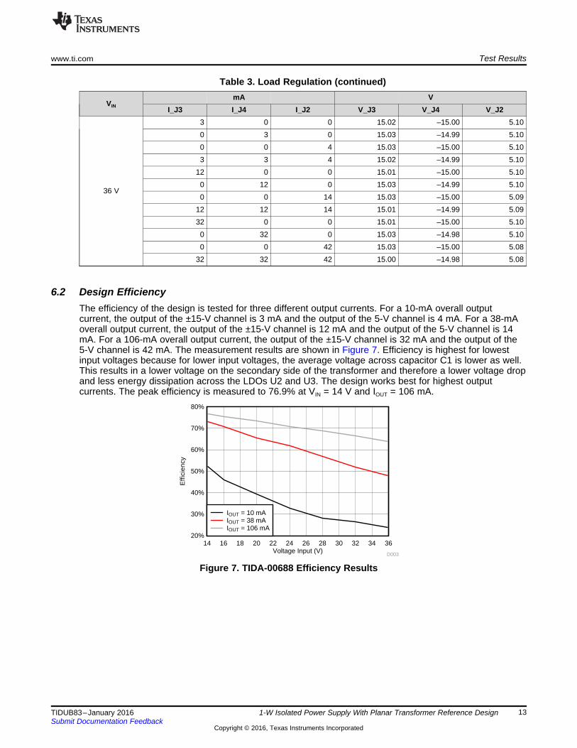
6.2 Design EfficiencyThe efficiency of the design is tested for three different output currents. For a 10-mA overall outputcurrent, the output of the ±15-V channel is 3 mA and the output of the 5-V channel is 4 mA. For a 38-mAoverall output current, the output of the ±15-V channel is 12 mA and the output of the 5-V channel is 14mA. For a 106-mA overall output current, the output of the ±15-V channel is 32 mA and the output of the5-V channel is 42 mA. The measurement results are shown in Figure 7. Efficiency is highest for lowestinput voltages because for lower input voltages, the average voltage across capacitor C1 is lower as well.This results in a lower voltage on the secondary side of the transformer and therefore a lower voltage dropand less energy dissipation across the LDOs U2 and U3. The design works best for highest outputcurrents. The peak efficiency is measured to 76.9% at VIN = 14 V and IOUT = 106 mA.
Figure 7. TIDA-00688 Efficiency Results

Test Results www.ti.com
14 TIDUB83–January 2016Submit Documentation Feedback
Copyright © 2016, Texas Instruments Incorporated
1-W Isolated Power Supply With Planar Transformer Reference Design
6.3 Startup and Shutdown SequenceFigure 8 and Figure 9 show the startup and shutdown sequences for the 12-V, 24-V, and 36-V inputvoltages. The 12-V input voltage is tested to showcase what is happening if the input voltage drops belowthe specified 14 V. With just the 12-V input voltage, the design starts working without any problems.However, the output of the ±15-V channels are slightly too low for the LDO’s minimum drop voltage to beregulated. Therefore, the design should only be operated within 14- to 36-V input voltage. The UVLO isset to 12 V with resistors R2 and R3.
The startup time goes from 18 ms for the 12-V input voltage down to 12 ms for the 36-V input voltage. Forall sequences, as soon as the supply voltage of the LM5017 reaches 12 V, the LM5017 starts operatingand the three secondary outputs are enabled. The output of the TPS62175 is enabled in about 1 ms. Theregulated LDO outputs take about 10 ms until they reach their final output voltage.
The shutdown sequences look very similar to each other. As soon as the input voltage falls below 12 V,the LM5017 stops working and the secondary outputs are disabled. Then, the outputs caps aredischarged.
Figure 8. Startup Sequences for VIN = 12 V, 24 V, 36 V

www.ti.com Test Results
15TIDUB83–January 2016Submit Documentation Feedback
Copyright © 2016, Texas Instruments Incorporated
1-W Isolated Power Supply With Planar Transformer Reference Design
Figure 9. Shutdown Sequences for VIN = 12 V, 24 V, 36 V

Test Results www.ti.com
16 TIDUB83–January 2016Submit Documentation Feedback
Copyright © 2016, Texas Instruments Incorporated
1-W Isolated Power Supply With Planar Transformer Reference Design
6.4 Switch NodeFigure 10 shows the switching behavior of the LM5017 for input voltages of 12, 24, and 36 V, which is thatthe duty cycle is higher for lower input voltages. As a result of the COT switching behavior of the LM5017,the switching frequency differs with the input voltage as well.
The duty cycle goes from 73% for 12-V input voltage down to 33% for 36-V input voltage.
Figure 10. Switching of LM5017 for VIN = 12 V, 24 V, 36 V

www.ti.com Test Results
17TIDUB83–January 2016Submit Documentation Feedback
Copyright © 2016, Texas Instruments Incorporated
1-W Isolated Power Supply With Planar Transformer Reference Design
6.5 Thermal MeasurementFigure 11 shows thermal pictures of the board for different input voltages under full load condition. Thepictures were captured with a FLUKE Ti40FT at 25°C room temperature. The images show that the ferritestays cool for the complete input voltage range. In the case of VIN = 36 V, the maximum temperature onthe board is at the LM5017, which reaches 48°C. The circuit is designed for temperatures of up to 125°C.Therefore, the board can be operated at ambient temperatures of up to 85°C.
Figure 11. Thermal Pictures of TIDA-00688 for VIN = 12 V, 24 V, 36 V

453k
R4
11.8k
R8
2.00kR6
2.00kR3
16.9kR2
0R9
GND GNDGND
D1
CDBU0245
GND
0.01µF
C4
D2
RF081M2STR
D3
RF081M2STRL1LQM18PN2R2MFH 600 ohm
L7
600 ohmL6
4.7µFC8
4.7µFC25
4.7µFC26
GNDS
0.1µFC28
0.1µFC29
0.1µFC2
GNDGNDGNDGND
1
2
J4
1
2
J3
1
2
J1
0.01µF
C20
0.01µF
C21
0.01µF
C22
0.01µF
C23
GNDA
23.7k
R18
23.2k
R17
2.00kR16
2.00kR15
4.7µFC9
1.5µFC1
1000pF
C11
GND GNDS
0
R12
GNDA GNDA GNDA GNDA GNDA
GNDAGNDAGNDAGNDAGNDAGNDS
GNDA GNDA
600 ohmL4
600 ohmL2
600 ohmL3
0.1µFC18
0.1µFC19
GNDA
GNDA
Guard Ring
Guard ring connection with signal ground
All ground connections insidethe guard ring will bereferenced to the analogoutput ground to minimizenoise and error
50 mA
30 mAP=1.44W
9V
L=
56u
H
U = 12V .. 36V
PI-Filter 1 Ohm 150 kHzeffective cap C1, C3 1.3uF
+15 V, 30 mA
-15 V, 30 mA
600 ohmL8
0.1µFC30
10.0kR20
53.6kR19
L5
VLS3010ET-220M
2.2µFC17
10µFC27
GNDS GNDS GNDS GNDS GNDS GNDS
1
2
J2
1000pFC24
AGND6
NC4
EN3
FB5
PG7
VIN2
VOS10
SW9
PGND1
PAD11
SLEEP8
U4
1.00
R1
2.2µFC14
2.2µFC3
Transients of 80V up to 20us
1µFC15
1µFC16
GNDA
GNDA
0
R13
0
R14
OUT1
FB2
GND4
EN5
NR/SS6
IN8
PAD9
U3
TPS7A3001DGN
OUT1
FB2
GND4
EN5
NR/SS6
IN8
PAD9
U2
TPS7A4901DGN
1.00k
R11DNP
56pF
C12
DNP
GND
470pFC10
1.00R10
27.4kR5
0.015µF
C13
DNP
0.1µFC6
0.022µFC7
GND
1µFC5
42.2R7
GND
RTN1
VIN2
UVLO3
RON4
FB5
VCC6
BST7
SW8
EP9
U1
LM5017SDX/NOPB
24V
D4BZT52C24T-7
NT1Net-Tie
NT2Net-Tie
NT3Net-Tie
Design Files www.ti.com
18 TIDUB83–January 2016Submit Documentation Feedback
Copyright © 2016, Texas Instruments Incorporated
1-W Isolated Power Supply With Planar Transformer Reference Design
7 Design Files
7.1 SchematicsTo download the schematics, see the design files at TIDA-00688.
Figure 12. 1-W Isolated Power Supply With Planar Transformer Schematic
space
space
space
space

www.ti.com Design Files
19TIDUB83–January 2016Submit Documentation Feedback
Copyright © 2016, Texas Instruments Incorporated
1-W Isolated Power Supply With Planar Transformer Reference Design
7.2 Bill of MaterialsTo download the bill of materials (BOM), see the design files at TIDA-00688.
Table 4. TIDA-00688 BOM
ITEM DESIGNATOR QTY VALUE PARTNUMBER MANUFACTURER DESCRIPTION PACKAGEREFERENCE
1 !PCB 1 TIDA-00688 Any Printed Circuit Board
2 C1 1 1.5uF GRM21BR71E155KA88L MuRata CAP, CERM, 1.5 µF, 25 V, +/-10%, X7R, 0805 0805
3 C2, C18, C19, C28, C29,C30 6 0.1uF C1608X7R1H104K TDK CAP, CERM, 0.1 µF, 50 V, +/-
10%, X7R, 0603 0603
4 C3, C14 2 2.2uF UMK316B7225KD-T Taiyo Yuden CAP, CERM, 2.2 µF, 50 V, +/-10%, X7R, 1206 1206
5 C4, C20, C21, C22, C23 5 0.01uF C0603C103J5RACTU Kemet CAP, CERM, 0.01 µF, 50 V,+/- 5%, X7R, 0603 0603
6 C5 1 1uF GRM188R71E105KA12D MuRata CAP, CERM, 1 µF, 25 V, +/-10%, X7R, 0603 0603
7 C6 1 0.1uF GCM188R71H104KA57D MuRata CAP, CERM, 0.1 µF, 50 V, +/-10%, X7R, 0603 0603
8 C7 1 0.022uF GRM188R71H223KA01D MuRata CAP, CERM, 0.022 µF, 50 V,+/- 10%, X7R, 0603 0603
9 C8, C9 2 4.7uF GRM31CR71E475KA88L MuRata CAP, CERM, 4.7 µF, 25 V, +/-10%, X7R, 1206 1206
10 C10 1 470pF C0603C471K5RACTU Kemet CAP, CERM, 470 pF, 50 V, +/-10%, X7R, 0603 0603
11 C11 1 1000pF 202R18W102KV4E Johanson Technology CAP, CERM, 1000 pF, 2000V, +/- 10%, X7R, 1206_190 1206_190
12 C15, C16 2 1uF C0603C105K3RACTU Kemet CAP, CERM, 1 µF, 25 V, +/-10%, X7R, 0603 0603
13 C17 1 2.2uF C2012X7R1V225K085AC TDK CAP, CERM, 2.2 µF, 35 V, +/-10%, X7R, 0805 0805
14 C24 1 1000pF GRM188R71E102KA01D MuRata CAP, CERM, 1000 pF, 25 V,+/- 10%, X7R, 0603 0603
15 C25, C26 2 4.7uF C3216X7R1E475K085AB TDK CAP, CERM, 4.7 µF, 25 V, +/-10%, X7R, 1206 1206
16 C27 1 10uF C3216X7R1A106M085AC TDK CAP, CERM, 10 µF, 10 V, +/-20%, X7R, 1206 1206
17 D1 1 45V CDBU0245 Comchip Technology Diode, Schottky, 45 V, 0.2 A,SOD-523F SOD-523F
18 D2, D3 2 200V RF081M2STR Rohm Diode, Fast Rectifier, 200 V,0.8 A, SOD-123 SOD-123

Design Files www.ti.com
20 TIDUB83–January 2016Submit Documentation Feedback
Copyright © 2016, Texas Instruments Incorporated
1-W Isolated Power Supply With Planar Transformer Reference Design
Table 4. TIDA-00688 BOM (continued)
ITEM DESIGNATOR QTY VALUE PARTNUMBER MANUFACTURER DESCRIPTION PACKAGEREFERENCE
19 D4 1 24V BZT52C24T-7 Diodes Inc. Diode, Zener, 24 V, 300 mW,SOD-523 SOD-523
20 FID1, FID2, FID3 3 N/A N/A Fiducial mark. There is nothingto buy or mount. N/A
21 H1, H4 2 B66284F2204X TDK CLAMP ELP 18X4X10 I18X2X10
22 H2 1 2.9 uH B66283PX187 TDK FERRITE CORE ELP 2.9UHN87
23 H3 1 2.6uH B66283GX187 TDK Ferrite Core, ELP, 2.6uH, N87
24 J1, J2, J3, J4 4 2x1 1751248 Phoenix Contact Conn Term Block, 2POS,3.5mm, TH 11x8.5x7.3mm
25 L1 1 2.2uH LQM18PN2R2MFH MuRata Inductor, Ferrite, 2.2 µH, 0.35A, 0.38 ohm, SMD 0603
26 L2, L3, L4, L6, L7, L8 6 600 ohm BLM18KG601SN1D MuRata Ferrite Bead, 600 ohm @ 100MHz, 1.3 A, 0603 0603
27 L5 1 22uH VLS3010ET-220M TDK Inductor, Shielded, Ferrite, 22µH, 0.38 A, 0.9 ohm, SMD Inductor, 3x1x3mm
28 R1, R10 2 1.00 CRCW06031R00FKEA Vishay-Dale RES, 1.00, 1%, 0.1 W, 0603 060329 R2 1 16.9k CRCW060316K9FKEA Vishay-Dale RES, 16.9 k, 1%, 0.1 W, 0603 060330 R3, R6, R15, R16 4 2.00k CRCW06032K00FKEA Vishay-Dale RES, 2.00 k, 1%, 0.1 W, 0603 060331 R4 1 453k CRCW0603453KFKEA Vishay-Dale RES, 453 k, 1%, 0.1 W, 0603 060332 R5 1 27.4k CRCW060327K4FKEA Vishay-Dale RES, 27.4 k, 1%, 0.1 W, 0603 060333 R7 1 42.2 CRCW060342R2FKEA Vishay-Dale RES, 42.2, 1%, 0.1 W, 0603 060334 R8 1 11.8k CRCW060311K8FKEA Vishay-Dale RES, 11.8 k, 1%, 0.1 W, 0603 060335 R9, R13, R14 3 0 ERJ-3GEY0R00V Panasonic RES, 0, 5%, 0.1 W, 0603 060336 R12 1 0 CRCW06030000Z0EA Vishay-Dale RES, 0, 5%, 0.1 W, 0603 060337 R17 1 23.2k CRCW060323K2FKEA Vishay-Dale RES, 23.2 k, 1%, 0.1 W, 0603 060338 R18 1 23.7k CRCW060323K7FKEA Vishay-Dale RES, 23.7 k, 1%, 0.1 W, 0603 060339 R19 1 53.6k CRCW060353K6FKEA Vishay-Dale RES, 53.6 k, 1%, 0.1 W, 0603 060340 R20 1 10.0k CRCW060310K0FKEA Vishay-Dale RES, 10.0 k, 1%, 0.1 W, 0603 0603
41 U1 1 LM5017SDX/NOPB Texas Instruments100V, 600mA Constant On-Time Synchronous BuckRegulator, NGU0008B
NGU0008B
42 U2 1 TPS7A4901DGN Texas Instruments+36V, +150mA, Ultralow-Noise, Positive LINEARREGULATOR, DGN0008D
DGN0008D

www.ti.com Design Files
21TIDUB83–January 2016Submit Documentation Feedback
Copyright © 2016, Texas Instruments Incorporated
1-W Isolated Power Supply With Planar Transformer Reference Design
Table 4. TIDA-00688 BOM (continued)
ITEM DESIGNATOR QTY VALUE PARTNUMBER MANUFACTURER DESCRIPTION PACKAGEREFERENCE
43 U3 1 TPS7A3001DGN Texas Instruments
-36V, -200mA, Ultralow-Noise,High PSRR, Adjustable -1.18to -33 V Output, NegativeLinear Regulator, 8-pin MSOP(DGN), -40 to 125 degC,Green (RoHS & no Sb/Br)
DGN0008D
44 U4 1 TPS62175DQCR Texas Instruments28V, 0.5A Step-DownConverter with Sleep Mode,DQC0010A
DQC0010A
45 C12 0 56pF GRM21A5C2E560JW01D MuRata CAP, CERM, 56 pF, 250 V, +/-5%, C0G/NP0, 0805 0805
46 C13 0 0.015uF GRM188R71H153KA01D MuRata CAP, CERM, 0.015 µF, 50 V,+/- 10%, X7R, 0603 0603
47 R11 0 1.00k CRCW08051K00FKEA Vishay-Dale RES, 1.00 k, 1%, 0.125 W,0805 0805

Design Files www.ti.com
22 TIDUB83–January 2016Submit Documentation Feedback
Copyright © 2016, Texas Instruments Incorporated
1-W Isolated Power Supply With Planar Transformer Reference Design
7.3 PCB Layout RecommendationsThe PCB layout is driven by two requirements: First, a small form-factor, and second, usability in theindustrial environment, meaning working at ambient temperatures of up to 85°C, low EMI, and low noise.
To achieve a small form factor, place all components very near to each other while keeping design andplacement rules in mind. To keep tracks also short, distribute components on both sides of the PCB. Tokeep cost low, only use 0603-sized or larger components in the design.
To get the planar transformer onto the board, use a four-layer design. Both sides of the board have aGND plane with 35-μm copper. As a result, every IC on the board has enough copper around it todistribute heat, and the design can be operated at ambient temperatures of up to 85°C. The secondaryanalog section of the board also has guard rings on the top and bottom layers to reduce EMI and noise.
Figure 13 shows the path of the current for one switching cycle. During toff, current follows the dashedpath from capacitor C1 on the left into the planar transformer (not shown), then through the switching nodeand the low-side FET of the LM5017 to GND, and back to C1. Also during toff, C1 serves as a local powersupply.
During ton, current follows the dotted path from capacitor C3 on the right through the high-side FET of theLM5017 into the planar transformer (not shown) to capacitor C1 and back to C3. Also during ton, C3serves as a local power supply.
To keep the current path short and switching noise low, place C1 and C3 close to the LM5017. Figure 13shows an exemplary layout where these requirements are fulfilled.
Figure 13. Layout Recommendation LM5017
www.ti.com Design Files
23TIDUB83–January 2016Submit Documentation Feedback
Copyright © 2016, Texas Instruments Incorporated
1-W Isolated Power Supply With Planar Transformer Reference Design
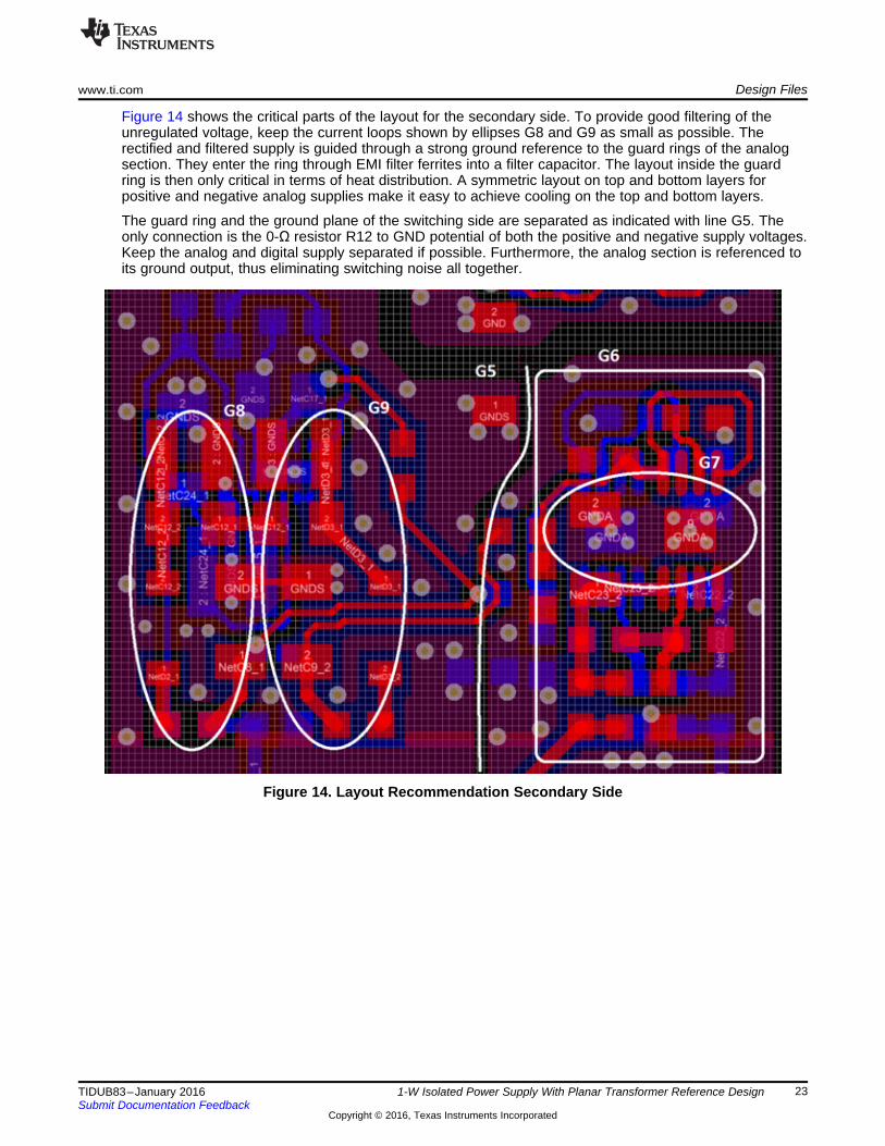
Figure 14 shows the critical parts of the layout for the secondary side. To provide good filtering of theunregulated voltage, keep the current loops shown by ellipses G8 and G9 as small as possible. Therectified and filtered supply is guided through a strong ground reference to the guard rings of the analogsection. They enter the ring through EMI filter ferrites into a filter capacitor. The layout inside the guardring is then only critical in terms of heat distribution. A symmetric layout on top and bottom layers forpositive and negative analog supplies make it easy to achieve cooling on the top and bottom layers.
The guard ring and the ground plane of the switching side are separated as indicated with line G5. Theonly connection is the 0-Ω resistor R12 to GND potential of both the positive and negative supply voltages.Keep the analog and digital supply separated if possible. Furthermore, the analog section is referenced toits ground output, thus eliminating switching noise all together.
Figure 14. Layout Recommendation Secondary Side

Design Files www.ti.com
24 TIDUB83–January 2016Submit Documentation Feedback
Copyright © 2016, Texas Instruments Incorporated
1-W Isolated Power Supply With Planar Transformer Reference Design
7.3.1 Layer PlotsTo download the layer plots, see the design files at TIDA-00688.
Figure 15. Top Overlay Figure 16. Top Solder Mask Figure 17. Top Layer
Figure 18. Mid Layer 1 Figure 19. Mid Layer 2 Figure 20. Bottom Layer

www.ti.com Design Files
25TIDUB83–January 2016Submit Documentation Feedback
Copyright © 2016, Texas Instruments Incorporated
1-W Isolated Power Supply With Planar Transformer Reference Design
Figure 21. Bottom Solder Mask Figure 22. Bottom Overlay Figure 23. Drill Drawing
Figure 24. Board Dimensions
7.4 Altium ProjectTo download the Altium project files, see the design files at TIDA-00688.
7.5 Gerber FilesTo download the Gerber files, see the design files at TIDA-00688.
7.6 Assembly DrawingsTo download the assembly drawings, see the design files at TIDA-00688.

References www.ti.com
26 TIDUB83–January 2016Submit Documentation Feedback
Copyright © 2016, Texas Instruments Incorporated
1-W Isolated Power Supply With Planar Transformer Reference Design
8 References
1. Texas Instruments, 1-W Small Form Factor Power Supply with Isolated Dual Output for PLC I/OModules, TIDA-00129 Design Guide (TIDU263)
2. Texas Instruments, Ultra-Thin, Small Footprint 1-W, 12- to 36-V Isolated Power Supply With ±15 V and5 V for Analog PLC Modules, TIDA-00237 Design Guide (TIDU855)
3. Texas Instruments, AN-2292 Designing an Isolated Buck (Fly-Buck) Converter, Fly-Buck ApplicationNote (SNVA674)
9 About the AuthorsTOBIAS PUETZ is a systems engineer in the Texas Instruments Factory Automation and Control team,where he is working on PLC modules. Tobias brings to this role his expertise in different sensingtechnologies, power design, and wireless charging as well as software design. Tobias earned his master'sdegree in electrical engineering and information technology at the Karlsruhe Institute of Technology (KIT),Germany in 2014.
INGOLF FRANK is a systems engineer in the Texas Instruments Factory Automation and Control team,focusing on PLC I/O modules. Ingolf works across multiple product families and technologies to leveragethe best solutions possible for system level application design. Ingolf earned his electrical engineeringdegree (Dipl. Ing. (FH)) in the field of information technology at the University of Applied SciencesBielefeld, Germany in 1991.

IMPORTANT NOTICE FOR TI REFERENCE DESIGNS
Texas Instruments Incorporated ("TI") reference designs are solely intended to assist designers (“Buyers”) who are developing systems thatincorporate TI semiconductor products (also referred to herein as “components”). Buyer understands and agrees that Buyer remainsresponsible for using its independent analysis, evaluation and judgment in designing Buyer’s systems and products.TI reference designs have been created using standard laboratory conditions and engineering practices. TI has not conducted anytesting other than that specifically described in the published documentation for a particular reference design. TI may makecorrections, enhancements, improvements and other changes to its reference designs.Buyers are authorized to use TI reference designs with the TI component(s) identified in each particular reference design and to modify thereference design in the development of their end products. HOWEVER, NO OTHER LICENSE, EXPRESS OR IMPLIED, BY ESTOPPELOR OTHERWISE TO ANY OTHER TI INTELLECTUAL PROPERTY RIGHT, AND NO LICENSE TO ANY THIRD PARTY TECHNOLOGYOR INTELLECTUAL PROPERTY RIGHT, IS GRANTED HEREIN, including but not limited to any patent right, copyright, mask work right,or other intellectual property right relating to any combination, machine, or process in which TI components or services are used.Information published by TI regarding third-party products or services does not constitute a license to use such products or services, or awarranty or endorsement thereof. Use of such information may require a license from a third party under the patents or other intellectualproperty of the third party, or a license from TI under the patents or other intellectual property of TI.TI REFERENCE DESIGNS ARE PROVIDED "AS IS". TI MAKES NO WARRANTIES OR REPRESENTATIONS WITH REGARD TO THEREFERENCE DESIGNS OR USE OF THE REFERENCE DESIGNS, EXPRESS, IMPLIED OR STATUTORY, INCLUDING ACCURACY ORCOMPLETENESS. TI DISCLAIMS ANY WARRANTY OF TITLE AND ANY IMPLIED WARRANTIES OF MERCHANTABILITY, FITNESSFOR A PARTICULAR PURPOSE, QUIET ENJOYMENT, QUIET POSSESSION, AND NON-INFRINGEMENT OF ANY THIRD PARTYINTELLECTUAL PROPERTY RIGHTS WITH REGARD TO TI REFERENCE DESIGNS OR USE THEREOF. TI SHALL NOT BE LIABLEFOR AND SHALL NOT DEFEND OR INDEMNIFY BUYERS AGAINST ANY THIRD PARTY INFRINGEMENT CLAIM THAT RELATES TOOR IS BASED ON A COMBINATION OF COMPONENTS PROVIDED IN A TI REFERENCE DESIGN. IN NO EVENT SHALL TI BELIABLE FOR ANY ACTUAL, SPECIAL, INCIDENTAL, CONSEQUENTIAL OR INDIRECT DAMAGES, HOWEVER CAUSED, ON ANYTHEORY OF LIABILITY AND WHETHER OR NOT TI HAS BEEN ADVISED OF THE POSSIBILITY OF SUCH DAMAGES, ARISING INANY WAY OUT OF TI REFERENCE DESIGNS OR BUYER’S USE OF TI REFERENCE DESIGNS.TI reserves the right to make corrections, enhancements, improvements and other changes to its semiconductor products and services perJESD46, latest issue, and to discontinue any product or service per JESD48, latest issue. Buyers should obtain the latest relevantinformation before placing orders and should verify that such information is current and complete. All semiconductor products are soldsubject to TI’s terms and conditions of sale supplied at the time of order acknowledgment.TI warrants performance of its components to the specifications applicable at the time of sale, in accordance with the warranty in TI’s termsand conditions of sale of semiconductor products. Testing and other quality control techniques for TI components are used to the extent TIdeems necessary to support this warranty. Except where mandated by applicable law, testing of all parameters of each component is notnecessarily performed.TI assumes no liability for applications assistance or the design of Buyers’ products. Buyers are responsible for their products andapplications using TI components. To minimize the risks associated with Buyers’ products and applications, Buyers should provideadequate design and operating safeguards.Reproduction of significant portions of TI information in TI data books, data sheets or reference designs is permissible only if reproduction iswithout alteration and is accompanied by all associated warranties, conditions, limitations, and notices. TI is not responsible or liable forsuch altered documentation. Information of third parties may be subject to additional restrictions.Buyer acknowledges and agrees that it is solely responsible for compliance with all legal, regulatory and safety-related requirementsconcerning its products, and any use of TI components in its applications, notwithstanding any applications-related information or supportthat may be provided by TI. Buyer represents and agrees that it has all the necessary expertise to create and implement safeguards thatanticipate dangerous failures, monitor failures and their consequences, lessen the likelihood of dangerous failures and take appropriateremedial actions. Buyer will fully indemnify TI and its representatives against any damages arising out of the use of any TI components inBuyer’s safety-critical applications.In some cases, TI components may be promoted specifically to facilitate safety-related applications. With such components, TI’s goal is tohelp enable customers to design and create their own end-product solutions that meet applicable functional safety standards andrequirements. Nonetheless, such components are subject to these terms.No TI components are authorized for use in FDA Class III (or similar life-critical medical equipment) unless authorized officers of the partieshave executed an agreement specifically governing such use.Only those TI components that TI has specifically designated as military grade or “enhanced plastic” are designed and intended for use inmilitary/aerospace applications or environments. Buyer acknowledges and agrees that any military or aerospace use of TI components thathave not been so designated is solely at Buyer's risk, and Buyer is solely responsible for compliance with all legal and regulatoryrequirements in connection with such use.TI has specifically designated certain components as meeting ISO/TS16949 requirements, mainly for automotive use. In any case of use ofnon-designated products, TI will not be responsible for any failure to meet ISO/TS16949.IMPORTANT NOTICE
Mailing Address: Texas Instruments, Post Office Box 655303, Dallas, Texas 75265Copyright © 2016, Texas Instruments Incorporated