12-bit, parallel input digital-to-analog converter … · 12-bit, parallel input digital-to-analog...
TRANSCRIPT

®
12-Bit, Parallel InputDIGITAL-TO-ANALOG CONVERTER
DESCRIPTIONThe DAC7621 is a 12-bit digital-to-analog converter(DAC) with guaranteed 12-bit monotonicity perfor-mance over the industrial temperature range. It re-quires a single +5V supply and contains an inputregister, latch, 2.435V reference, DAC, and high speedrail-to-rail output amplifier. For a full-scale step, theoutput will settle to 1 LSB within 7µs. The deviceconsumes 2.5mW (0.5mA at 5V).
The parallel interface is compatible with a wide varietyof microcontrollers. The DAC7621 accepts a 12-bitparallel word, has a double-buffered input logic struc-ture and provides data readback. In addition, twocontrol pins provide a chip select (CS) function andasynchronous clear (CLR) input. The CLR input canbe used to ensure that the DAC7621 output is 0V onpower-up or as required by the application.
The DAC7621 is available in a 20-lead SSOP packageand is fully specified over the industrial temperaturerange of –40°C to +85°C.
FEATURES LOW POWER: 2.5mW
FAST SETTLING: 7 µs to 1 LSB
1mV LSB WITH 4.095V FULL-SCALERANGE
COMPLETE WITH REFERENCE
12-BIT LINEARITY AND MONOTONICITYOVER INDUSTRIAL TEMP RANGE
ASYNCHRONOUS RESET TO 0V
APPLICATIONS PROCESS CONTROL
DATA ACQUISITION SYSTEMS
CLOSED-LOOP SERVO-CONTROL
PC PERIPHERALS
PORTABLE INSTRUMENTATION
International Airport Industrial Park • Mailing Address: PO Box 11400, Tucson, AZ 85734 • Street Address: 6730 S. Tucson Bl vd., Tucson, AZ 85706 • Tel: (520) 746-1111Twx: 910-952-1111 • Internet: http://www.burr-brown.com/ • Cable: BBRCORP • Telex: 066-6491 • FAX: (520) 889-1510 • I mmediate Product Info: (800) 548-6132
®DAC7621
12-Bit DACRef
DAC Register
Input Register
I/O Buffer
12
12
12
CLR
LOADDAC
CS
R/W
VDD
VOUT
DGND
DAC7621
D0 D1 D2 D3 D4 D5 D6 D7 D8 D9 D10 D11
DAC7621
© 1998 Burr-Brown Corporation PDS-1502B Printed in U.S.A. March, 1999
For most current data sheet and other productinformation, visit www.burr-brown.com
SBAS107

®
2DAC7621
SPECIFICATIONSELECTRICALAt TA = –40°C to +85°C, and VDD = +5V, unless otherwise noted.
The information provided herein is believed to be reliable; however, BURR-BROWN assumes no responsibility for inaccuracies or omissions. BURR-BROWN assumesno responsibility for the use of this information, and all use of such information shall be entirely at the user’s own risk. Prices and specifications are subject to changewithout notice. No patent rights or licenses to any of the circuits described herein are implied or granted to any third party. BURR-BROWN does not authorize or warrantany BURR-BROWN product for use in life support devices and/or systems.
DAC7621E DAC7621EB
PARAMETER CONDITIONS MIN TYP MAX MIN TYP MAX UNITS
RESOLUTION 12 Bits
ACCURACYRelative Accuracy(1) –2 ±1/2 +2 –1 ±1/4 +1 LSBDifferential Nonlinearity Guaranteed Monotonic –1 ±1/2 +1 –1 ±1/4 +1 LSBZero-Scale Error Code 000H –1 +1 +3 LSBFull Scale Voltage Code FFFH 4.079 4.095 4.111 4.087 4.095 4.103 V
ANALOG OUTPUTOutput Current Code 800H ±5 ±7 mALoad Regulation RLOAD ≥ 402Ω, Code 800H 1 3 LSBCapacitive Load No Oscillation 500 pFShort-Circuit Current ±20 mAShort-Circuit Duration GND or VDD Indefinite
DIGITAL INPUTData Format Parallel
Data Coding Straight Binary
Logic Family CMOS
Logic LevelsVIH 0.7 • VDD VVIL 0.3 • VDD VIIH ±10 µAIIL ±10 µA
DYNAMIC PERFORMANCESettling Time(2) (tS) To ±1 LSB of Final Value 7 µsDAC Glitch 5 nV-sDigital Feedthrough 2 nV-s
POWER SUPPLYVDD +4.75 +5.0 +5.25 VIDD VIH = 5V, VIL = 0V, No Load, at Code 000H 0.5 1 mA
Power Dissipation VIH = 5V, VIL = 0V, No Load 2.5 5 mWPower Supply Sensitivity ∆VDD = ±5% 0.001 0.004 %/%
TEMPERATURE RANGESpecified Performance –40 +85 °C
Same specification as for DAC7621E.
NOTES: (1) This term is sometimes referred to as Linearity Error or Integral Nonlinearity (INL). (2) Specification does not apply to negative-going transitions wherethe final output voltage will be within 3 LSBs of ground. In this region, settling time may be double the value indicated.

®
3 DAC7621
PIN CONFIGURATION
Top View SSOP
VDD to GND .......................................................................... –0.3V to 6VDigital Inputs to GND .............................................. –0.3V to VDD + 0.3VVOUT to GND ...........................................................–0.3V to VDD + 0.3VPower Dissipation ........................................................................ 325mWThermal Resistance, θJA ........................................................... 150°C/WMaximum Junction Temperature .................................................. +150°COperating Temperature Range ...................................... –40°C to +85°CStorage Temperature Range ....................................... –65°C to +150°CLead Temperature (soldering, 10s) .............................................. +300°C
NOTE: (1) Stresses above those listed under “Absolute Maximum Ratings”may cause permanent damage to the device. Exposure to absolute maximumconditions for extended periods may affect device reliability.
ABSOLUTE MAXIMUM RATINGS (1)
PIN DESCRIPTIONS
PIN LABEL DESCRIPTION
1 CLR Reset. Resets the DAC register to zero. ActiveLOW. Asynchronous input.
2 VDD Postive Power Supply
3 VOUT DAC Output Voltage
4 AGND Analog Ground
5 DGND Digital Ground
6 DB11 Data Bit 11, MSB
7 DB10 Data Bit 10
8 DB9 Data Bit 9
9 DB8 Data Bit 8
10 DB7 Data Bit 7
11 DB6 Data Bit 6
12 DB5 Data Bit 5
13 DB4 Data Bit 4
14 DB3 Data Bit 3
15 DB2 Data Bit 2
16 DB1 Data Bit 1
17 DB0 Data Bit 0, LSB
18 R/W Read and Write Control
19 CS Chip Select. Active LOW.
20 LOADDAC Loads the internal DAC register. The DAC registeris a transparent latch and is transparent whenLOADDAC is LOW (regardless of the state of CS orCLK).
ELECTROSTATICDISCHARGE SENSITIVITY
This integrated circuit can be damaged by ESD. Burr-Brownrecommends that all integrated circuits be handled withappropriate precautions. Failure to observe proper handlingand installation procedures can cause damage.
ESD damage can range from subtle performance degrada-tion to complete device failure. Precision integrated circuitsmay be more susceptible to damage because very smallparametric changes could cause the device not to meet itspublished specifications.
PACKAGE/ORDERING INFORMATION
MINIMUMRELATIVE DIFFERENTIAL SPECIFICATION PACKAGE
ACCURACY NONLINEARITY TEMPERATURE DRAWING ORDERING TRANSPORTPRODUCT (LSB) (LSB) RANGE PACKAGE NUMBER (1) NUMBER(2) MEDIA
DAC7621E ±2 ±1 –40°C to +85°C 20-Lead SSOP 334 DAC7621E Rails" " " " " " DAC7621E/1K Tape and Reel
DAC7621EB ±1 ±1 –40°C to +85°C 20-Lead SSOP 334 DAC7621EB Rails" " " " " " DAC7621EB/1K Tape and Reel
NOTES: (1) For detailed drawing and dimension table, please see end of data sheet, or Appendix C of Burr-Brown IC Data Book. (2) Models with a slash (/) areavailable only in Tape and Reel in the quantities indicated (e.g., /1K indicates 1000 devices per reel). Ordering 1000 pieces of “DAC7621E/1K” will get a single1000-piece Tape and Reel. For detailed Tape and Reel mechanical information, refer to Appendix B of Burr-Brown IC Data Book.
1
2
3
4
5
6
7
8
9
10
20
19
18
17
16
15
14
13
12
11
CLR
VDD
VOUT
AGND
DGND
DB11 (MSB)
DB10
DB9
DB8
DB7
LOADDAC
CS
R/W
DB0 (LSB)
DB1
DB2
DB3
DB4
DB5
DB6
DAC7621E

®
4DAC7621
TIMING DIAGRAMS
LOGIC TRUTH TABLETIMING SPECIFICATIONSTA = –40°C to +85°C
SYMBOL DESCRIPTION MIN TYP MAX UNITS
tRCS CS LOW for Read 200 ns
tRDS R/W HIGH to CS LOW 10 ns
tRDH R/W HIGH after CS HIGH 0 ns
tDZ CS HIGH to Data Bus 100 nsin High Impedance
tCSD CS LOW to Data Bus Valid 100 160 ns
tWCS CS LOW for Write 50
tWS R/W LOW to CS LOW 0 ns
tWH R/W LOW after CS HIGH 5 ns
tDS Data Valid to CS LOW 0 ns
tDH Data Valid after CS HIGH 5 ns
tLWD LOADDAC LOW 50 ns
INPUT DACR/W CS LOADDAC REGISTER REGISTER MODE
L L L Write Write Write
L L H Write Hold Write Input
H L H Read Hold Read Input
X H L Hold Update Update
X H H Hold Hold Hold
X = Don’t Care.
tRCS
CS
tRDS tRDH
tCSD
tDZ
R/W
Data Out Data Valid
tWCS
CS
tWS tWH
R/W
tLWD
LOADDAC
tDS tDH
Data In
Data Output Timing Digital Input Timing
®
5 DAC7621
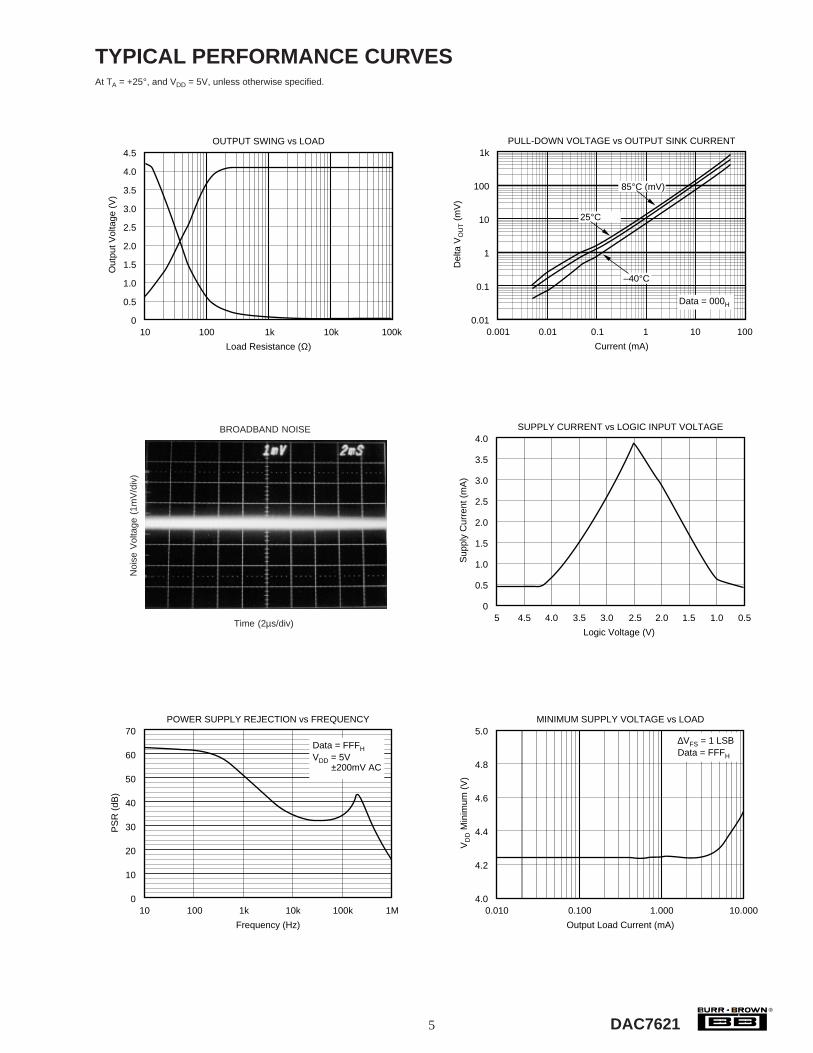
TYPICAL PERFORMANCE CURVESAt TA = +25°, and VDD = 5V, unless otherwise specified.
4.5
4.0
3.5
3.0
2.5
2.0
1.5
1.0
0.5
0
OUTPUT SWING vs LOAD
Out
put V
olta
ge (
V)
Load Resistance (Ω)
10 100 1k 10k 100k
1k
100
10
1
0.1
0.01
PULL-DOWN VOLTAGE vs OUTPUT SINK CURRENT
Del
ta V
OU
T (
mV
)
Current (mA)
0.001 0.01 0.1 1 10 100
85°C (mV)
–40°C
Data = 000H
25°C
4.0
3.5
3.0
2.5
2.0
1.5
1.0
0.5
0
SUPPLY CURRENT vs LOGIC INPUT VOLTAGE
Sup
ply
Cur
rent
(m
A)
Logic Voltage (V)
5 4.5 4.0 3.5 3.0 2.5 2.0 1.5 1.0 0.5
70
60
50
40
30
20
10
0
POWER SUPPLY REJECTION vs FREQUENCY
PS
R (
dB)
Frequency (Hz)
10 100 1k 10k 100k 1M
Data = FFFHVDD = 5V
±200mV AC
5.0
4.8
4.6
4.4
4.2
4.0
MINIMUM SUPPLY VOLTAGE vs LOAD
VD
D M
inim
um (
V)
Output Load Current (mA)
0.010 0.100 1.000 10.000
∆VFS = 1 LSBData = FFFH
BROADBAND NOISE
Noi
se V
olta
ge (
1mV
/div
)
Time (2µs/div)
Code = FFFHBW = 2MHz

®
6DAC7621
TYPICAL PERFORMANCE CURVES (CONT)At TA = +25°, and VDD = 5V, unless otherwise specified.
80
60
40
20
0
–20
–40
–60
–80
SHORT-CIRCUIT CURRENT vs OUTPUT VOLTAGE
Out
put C
urre
nt (
mA
)
Output Voltage (V)
0 0.5 1.0 1.5 2.0 2.5 3.0 3.5 4.0 4.5 5.0
PositiveCurrent
Limit
Data = 800HOutput tied to ISOURCE
NegativeCurrent
Limit
4.0
3.5
3.0
2.5
2.0
1.5
1.0
0.5
0
SUPPLY CURRENT vs TEMPERATURE
Sup
ply
Cur
rent
(m
A)
Temperature (°C)
–40 –30 –20 –10 0 10 20 30 40 50 60 70 80 90
VLOGIC = 3.5VData = FFFHNo Load
VDD = 4.75V
VDD = 5.25V VDD = 5.0V
LARGE-SIGNAL SETTLING TIME
1V/d
iv
Time (20µs/div)
CL = 110pFRL = No Load
LD
VOUT
RISE TIME DETAIL
Out
put V
olta
ge (
1mV
/div
)
Time (10µs/div)
LD
VOUT
MID-SCALE GLITCH PERFORMANCE
VO
UT (
2mV
/div
)
Time (500ns/div)
VOUT
LOADDAC
7FFH to 800H
MID-SCALE GLITCH PERFORMANCE
VO
UT (
2mV
/div
)
Time (500ns/div)
LOADDAC
800H to 7FFH
VOUT

®
7 DAC7621
TYPICAL PERFORMANCE CURVES (CONT)At TA = +25°, and VDD = 5V, unless otherwise specified.
FALL TIME DETAILO
utpu
t Vol
tage
(1m
V/d
iv)
Time (10µs/div)
LD
VOUT
10.000
1.000
0.100
0.010
OUTPUT VOLTAGE NOISE vs FREQUENCY
Noi
se (
µV/√
Hz)
Frequency (Hz)
10 100 1k 10k 100k
Data = FFFH
8
6
4
2
0
–2
–4
–6
–8
Out
put V
olta
ge C
hang
e (m
V)
Hours of Operation at +150°C
LONG-TERM DRIFT ACCELERATED BY BURN-IN
0 400200 600 800 1000 1200
avg
max
min
144 Units
0
10
20
30
40
50
60
–12 –8 –4 0 4 8 12
T.U.E = ΣINL = ZS + FSSample Size = 300 Units
TA = +25°CN
umbe
r of
Uni
ts
TOTAL UNADJUSTED ERROR HISTOGRAM
4.115
4.110
4.105
4.100
4.095
4.090
4.085
4.080
4.075
FULL-SCALE VOLTAGE vs TEMPERATURE
Ful
l-Sca
le O
utpu
t (V
)
Temperature (°C)
–50 0 25–25 50 75 100 125
No LoadSample Size = 300Avg + 3σ
Avg – 3σ
Avg
3
2
1
0
–1
ZERO-SCALE VOLTAGE vs TEMPERATURE
Zer
o-S
cale
(m
V)
Temperature (°C)
–50 0 25–25 50 75 100 125

®
8DAC7621
TYPICAL PERFORMANCE CURVES (CONT)At TA = +25°, and VDD = 5V, unless otherwise specified.
LINEARITY ERROR vs DIGITAL CODE(at +25°C)
Line
arity
Err
or (
LSB
s)
0
2.0
1.5
1.0
0.5
0
–0.5
–1.0
–1.5
–2.0512 1024 1536 2048 2560 3072 3584 4096
Code
DIFFERENTIAL LINEARITY ERROR vs DIGITAL CODE(at +25°C)
Diff
eren
tial L
inea
rity
Err
or (
LSB
s)
0
2.0
1.5
1.0
0.5
0
–0.5
–1.0
–1.5
–2.0512 1024 1536 2048 2560 3072 3584 4096
Code
LINEARITY ERROR vs DIGITAL CODE(at +85°C)
Line
arity
Err
or (
LSB
s)
0
1
0.5
0
–0.5
–1.0512 1024 1536 2048 2560 3072 3584 4096
Code
DIFFERENTIAL LINEARITY ERROR vs DIGITAL CODE(at +85°C)
Diff
eren
tial L
inea
rity
Err
or (
LSB
s)
0
1
0.5
0
–0.5
–1.0512 1024 1536 2048 2560 3072 3584 4096
Code
LINEARITY ERROR vs DIGITAL CODE(at –40°C)
Line
arity
Err
or (
LSB
s)
0
1
0.5
0
–0.5
–1.0512 1024 1536 2048 2560 3072 3584 4096
Code
DIFFERENTIAL LINEARITY ERROR vs DIGITAL CODE(at –40°C)
Diff
eren
tial L
inea
rity
Err
or (
LSB
s)
0
1
0.5
0
–0.5
–1.0512 1024 1536 2048 2560 3072 3584 4096
Code

®
9 DAC7621
The digital data into the DAC7621 is double-buffered. Thismeans that new data can be entered into the DAC withoutdisturbing the old data and the analog output of the con-verter. At some point after the data has been entered into theserial shift register, this data can be transferred into the DACregister. This transfer is accomplished with a HIGH to LOWtransition of the LOADDAC pin. However, the LOADDACpin makes the DAC register transparent. If new data be-comes available on the bus register while LOADDAC isLOW, the DAC output voltage will change as the datachanges. To prevent this, CS must be returned HIGH priorto changing data on the bus.
At any time, the contents of the DAC register can be set to000H (analog output equals 0V) by taking the CLR inputLOW. The DAC register will remain at this value until CLRis returned HIGH and LOADDAC is taken LOW to allowthe contents of the input register to be transferred to theDAC register. If LOADDAC is LOW when CLR is takenLOW, the DAC register will be set to 000H and the analogoutput driven to 0V. When CLR is returned HIGH, the DACregister and the analog output will respond accordingly.
DIGITAL-TO-ANALOG CONVERTER
The internal DAC section is a 12-bit voltage outputdevice that swings between ground and the internal ref-erence voltage. The DAC is realized by a laser-trimmedR-2R ladder network which is switched by N-channelMOSFETs. The DAC output is internally connected tothe rail-to-rail output operational amplifier.
OPERATIONThe DAC7621 is a 12-bit digital-to-analog converter (DAC)complete with an input shift register, DAC register, laser-trimmed 12-bit DAC, on-board reference, and a rail-to-railoutput amplifier. Figure 1 shows the basic operation of theDAC7621.
INTERFACE
Figure 1 shows the basic connection between amicrocontroller and the DAC7621. The interface consists ofa Read/Write (R/W), data, and a load DAC signal(LOADDAC). In addition, a chip select (CS) input is avail-able to enable the DAC7621 when there are multiple de-vices. The data format is Straight Binary. An asynchronousclear input (CLR) is provided to simplify start-up or periodicresets. Table I shows the relationship between input codeand output voltage.
DAC7621 Full-Scale Range = 4.095VLeast Significant Bit = 1mV
DIGITAL INPUT CODE ANALOG OUTPUTSTRAIGHT OFFSET BINARY (V) DESCRIPTION
FFFH +4.095 Full Scale801H +2.049 Midscale + 1 LSB800H +2.048 Midscale7FFH +2.047 Midscale – 1 LSB000H 0 Zero Scale
TABLE I. Digital Input Code and Corresponding IdealAnalog Output.
FIGURE 1. Basic Operation of the DAC7621.
1
2
3
4
5
6
7
8
9
10
20
19
18
17
16
15
14
13
12
11
CLR
VDD
VOUT
AGND
DGND
DB11
DB10
DB9
DB8
DB7
LOADDAC
CS
R/W
DB0
DB1
DB2
DB3
DB4
DB5
DB6
DAC7621E
Load DAC
Chip Select
Read/Write10µF
+5V
Clear
Data Bus
Data Bus
0V to+4.095V
0.1µF+

®
10DAC7621
OUTPUT AMPLIFIER
A precision, low-power amplifier buffers the output of theDAC section and provides additional gain to achieve a 0Vto 4.095V range. The amplifier has low offset voltage, lownoise, and a set gain of 1.682V/V (4.095/2.435). See Figure2 for an equivalent circuit schematic of the analog portionof the DAC7621.
The output amplifier has a 7µs typical settling time to ±1LSB of the final value. Note that there are differences in thesettling time for negative-going signals versus positive-going signals.
The rail-to-rail output stage of the amplifier provides thefull-scale range of 0V to 4.095V while operating on asupply voltage as low as 4.75V. In addition to its ability todrive resistive loads, the amplifier will remain stable whiledriving capacitive loads of up to 500pF. See Figure 3 for anequivalent circuit schematic of the amplifier’s output driverand the Typical Performance Curves section for more infor-mation regarding settling time, load driving capability, andoutput noise.
POWER SUPPLY
A BiCMOS process and careful design of the bipolar andCMOS sections of the DAC7621 result in a very low powerdevice. Bipolar transistors are used where tight matchingand low noise are needed to achieve analog accuracy, andCMOS transistors are used for logic, switching functionsand for other low power stages.
If power consumption is critical, it is important to keep thelogic levels on the digital inputs (R/W, CLK, CS, LOADDAC,CLR) as close as possible to either VDD or ground. This willkeep the CMOS inputs (see “Supply Current vs Logic InputVoltages” in the Typical Performance Curves) from shunt-ing current between VDD and ground.
The DAC7621 power supply should be bypassed as shownin Figure 1. The bypass capacitors should be placed as closeto the device as possible, with the 0.1µF capacitor takingpriority in this regard. The “Power Supply Rejection vsFrequency” graph in the Typical Performance Curves sec-tion shows the PSRR performance of the DAC7621. Thisshould be taken into account when using switching powersupplies or DC/DC converters.
In addition to offering guaranteed performance with VDD inthe 4.75V to 5.25V range, the DAC7621 will operate withreduced performance down to 4.5V. Operation between4.5V and 4.75V will result in longer settling time, reducedperformance, and current sourcing capability. Consult the“V DD vs Load Current” graph in the Typical PerformanceCurves section for more information.
FIGURE 3. Simplified Driver Section of Output Amplifier.
N-Channel
P-Channel
VDD
VOUT
AGND
2R
2R
2R
R
2R
2R
RR1
R
R2
Output AmplifierR-2R DAC
BandgapReference
2.435V
Buffer
FIGURE 2. Simplified Schematic of Analog Portion.

®
11 DAC7621
FIGURE 4. Suggested Power and Ground Connections for a DAC7621 Sharing a +5V Supply with a Digital System with aSingle Ground Plane.
APPLICATIONSPOWER AND GROUNDING
The DAC7621 can be used in a wide variety of situations—from low power, battery operated systems to large-scaleindustrial process control systems. In addition, some appli-cations require better performance than others, or are par-ticularly sensitive to one or two specific parameters. Thisdiversity makes it difficult to define definite rules to followconcerning the power supply, bypassing, and grounding.The following discussion must be considered in relation tothe desired performance and needs of the particular system.
A precision analog component requires careful layout, ad-equate bypassing, and a clean, well-regulated power supply.As the DAC7621 is a single-supply, +5V component, it willoften be used in conjunction with digital logic,microcontrollers, microprocessors, and digital signal proces-sors. The more digital logic present in the design and thehigher the switching speed, the more difficult it will be toachieve good performance.
The DAC7621 has separate analog ground and digital groundpins. The current through DGND is mostly switching tran-sients and are up to 4mA peak in amplitude. The currentthrough AGND is typically 0.5mA.
For best performance, separate analog and digital groundplanes with a single interconnection point to minimizeground loops. The analog pins are located adjacent to eachother to help isolate analog from digital signals. Analogsignals should be routed as far as possible from digital
signals and should cross them at right angles. A solid analogground plane around the D/A package, as well as under it inthe vicinity of the analog and power supply pins, will isolatethe D/A from switching currents. It is recommended thatDGND and AGND be connected directly to the groundplanes under the package.
If several DAC7621s are used, or if sharing supplies withother components, connecting the AGND and DGND linestogether at the power supplies once, rather than at each chip,may produce better results.
The power applied to VDD should be well regulated and low-noise. Switching power supplies and DC/DC converters willoften have high-frequency glitches or spikes riding on theoutput voltage. In addition, digital components can createsimilar high frequency spikes as their internal logic switchesstates. This noise can easily couple into the DAC outputvoltage through various paths between VDD and VOUT.
As with the GND connection, VDD should be connected toa +5V power supply plane or trace that is separate from theconnection for digital logic until they are connected at thepower entry point. In addition, the 10µF and 0.1µF capaci-tors shown in Figure 4 are strongly recommended andshould be installed as close to VDD and ground as possible.In some situations, additional bypassing may be requiredsuch as a 100µF electrolytic capacitor or even a “Pi” filtermade up of inductors and capacitors—all designed to essen-tially lowpass filter the +5V supply, removing the highfrequency noise (see Figure 4).
+
+5V
GND
100µF
Digital Circuits
+5V
GND
+5VPowerSupply
OtherAnalog
Components
VDD
AGND
DGND
DAC7621
+10µF 0.1µF
Optional

PACKAGE OPTION ADDENDUM
www.ti.com 25-Dec-2015
Addendum-Page 1
PACKAGING INFORMATION
Orderable Device Status(1)
Package Type PackageDrawing
Pins PackageQty
Eco Plan(2)
Lead/Ball Finish(6)
MSL Peak Temp(3)
Op Temp (°C) Device Marking(4/5)
Samples
DAC7621E ACTIVE SSOP DB 20 70 Green (RoHS& no Sb/Br)
CU NIPDAU Level-3-260C-168 HR -40 to 85 DAC7621E
DAC7621E/1K ACTIVE SSOP DB 20 1000 Green (RoHS& no Sb/Br)
CU NIPDAU Level-3-260C-168 HR -40 to 85 DAC7621E
DAC7621E/1KG4 ACTIVE SSOP DB 20 1000 Green (RoHS& no Sb/Br)
CU NIPDAU Level-3-260C-168 HR -40 to 85 DAC7621E
DAC7621EB ACTIVE SSOP DB 20 70 Green (RoHS& no Sb/Br)
CU NIPDAU Level-3-260C-168 HR -40 to 85 DAC7621EB
DAC7621EB/1K ACTIVE SSOP DB 20 1000 Green (RoHS& no Sb/Br)
CU NIPDAU Level-3-260C-168 HR -40 to 85 DAC7621EB
DAC7621EBG4 ACTIVE SSOP DB 20 70 Green (RoHS& no Sb/Br)
CU NIPDAU Level-3-260C-168 HR -40 to 85 DAC7621EB
DAC7621EG4 ACTIVE SSOP DB 20 70 Green (RoHS& no Sb/Br)
CU NIPDAU Level-3-260C-168 HR -40 to 85 DAC7621E
(1) The marketing status values are defined as follows:ACTIVE: Product device recommended for new designs.LIFEBUY: TI has announced that the device will be discontinued, and a lifetime-buy period is in effect.NRND: Not recommended for new designs. Device is in production to support existing customers, but TI does not recommend using this part in a new design.PREVIEW: Device has been announced but is not in production. Samples may or may not be available.OBSOLETE: TI has discontinued the production of the device.
(2) Eco Plan - The planned eco-friendly classification: Pb-Free (RoHS), Pb-Free (RoHS Exempt), or Green (RoHS & no Sb/Br) - please check http://www.ti.com/productcontent for the latest availabilityinformation and additional product content details.TBD: The Pb-Free/Green conversion plan has not been defined.Pb-Free (RoHS): TI's terms "Lead-Free" or "Pb-Free" mean semiconductor products that are compatible with the current RoHS requirements for all 6 substances, including the requirement thatlead not exceed 0.1% by weight in homogeneous materials. Where designed to be soldered at high temperatures, TI Pb-Free products are suitable for use in specified lead-free processes.Pb-Free (RoHS Exempt): This component has a RoHS exemption for either 1) lead-based flip-chip solder bumps used between the die and package, or 2) lead-based die adhesive used betweenthe die and leadframe. The component is otherwise considered Pb-Free (RoHS compatible) as defined above.Green (RoHS & no Sb/Br): TI defines "Green" to mean Pb-Free (RoHS compatible), and free of Bromine (Br) and Antimony (Sb) based flame retardants (Br or Sb do not exceed 0.1% by weightin homogeneous material)
(3) MSL, Peak Temp. - The Moisture Sensitivity Level rating according to the JEDEC industry standard classifications, and peak solder temperature.
(4) There may be additional marking, which relates to the logo, the lot trace code information, or the environmental category on the device.

PACKAGE OPTION ADDENDUM
www.ti.com 25-Dec-2015
Addendum-Page 2
(5) Multiple Device Markings will be inside parentheses. Only one Device Marking contained in parentheses and separated by a "~" will appear on a device. If a line is indented then it is a continuationof the previous line and the two combined represent the entire Device Marking for that device.
(6) Lead/Ball Finish - Orderable Devices may have multiple material finish options. Finish options are separated by a vertical ruled line. Lead/Ball Finish values may wrap to two lines if the finishvalue exceeds the maximum column width.
Important Information and Disclaimer:The information provided on this page represents TI's knowledge and belief as of the date that it is provided. TI bases its knowledge and belief on informationprovided by third parties, and makes no representation or warranty as to the accuracy of such information. Efforts are underway to better integrate information from third parties. TI has taken andcontinues to take reasonable steps to provide representative and accurate information but may not have conducted destructive testing or chemical analysis on incoming materials and chemicals.TI and TI suppliers consider certain information to be proprietary, and thus CAS numbers and other limited information may not be available for release.
In no event shall TI's liability arising out of such information exceed the total purchase price of the TI part(s) at issue in this document sold by TI to Customer on an annual basis.

TAPE AND REEL INFORMATION
*All dimensions are nominal
Device PackageType
PackageDrawing
Pins SPQ ReelDiameter
(mm)
ReelWidth
W1 (mm)
A0(mm)
B0(mm)
K0(mm)
P1(mm)
W(mm)
Pin1Quadrant
DAC7621E/1K SSOP DB 20 1000 330.0 16.4 8.2 7.5 2.5 12.0 16.0 Q1
DAC7621EB/1K SSOP DB 20 1000 330.0 16.4 8.2 7.5 2.5 12.0 16.0 Q1
PACKAGE MATERIALS INFORMATION
www.ti.com 15-Sep-2017
Pack Materials-Page 1

*All dimensions are nominal
Device Package Type Package Drawing Pins SPQ Length (mm) Width (mm) Height (mm)
DAC7621E/1K SSOP DB 20 1000 346.0 346.0 33.0
DAC7621EB/1K SSOP DB 20 1000 346.0 346.0 33.0
PACKAGE MATERIALS INFORMATION
www.ti.com 15-Sep-2017
Pack Materials-Page 2

IMPORTANT NOTICE
Texas Instruments Incorporated (TI) reserves the right to make corrections, enhancements, improvements and other changes to itssemiconductor products and services per JESD46, latest issue, and to discontinue any product or service per JESD48, latest issue. Buyersshould obtain the latest relevant information before placing orders and should verify that such information is current and complete.TI’s published terms of sale for semiconductor products (http://www.ti.com/sc/docs/stdterms.htm) apply to the sale of packaged integratedcircuit products that TI has qualified and released to market. Additional terms may apply to the use or sale of other types of TI products andservices.Reproduction of significant portions of TI information in TI data sheets is permissible only if reproduction is without alteration and isaccompanied by all associated warranties, conditions, limitations, and notices. TI is not responsible or liable for such reproduceddocumentation. Information of third parties may be subject to additional restrictions. Resale of TI products or services with statementsdifferent from or beyond the parameters stated by TI for that product or service voids all express and any implied warranties for theassociated TI product or service and is an unfair and deceptive business practice. TI is not responsible or liable for any such statements.Buyers and others who are developing systems that incorporate TI products (collectively, “Designers”) understand and agree that Designersremain responsible for using their independent analysis, evaluation and judgment in designing their applications and that Designers havefull and exclusive responsibility to assure the safety of Designers' applications and compliance of their applications (and of all TI productsused in or for Designers’ applications) with all applicable regulations, laws and other applicable requirements. Designer represents that, withrespect to their applications, Designer has all the necessary expertise to create and implement safeguards that (1) anticipate dangerousconsequences of failures, (2) monitor failures and their consequences, and (3) lessen the likelihood of failures that might cause harm andtake appropriate actions. Designer agrees that prior to using or distributing any applications that include TI products, Designer willthoroughly test such applications and the functionality of such TI products as used in such applications.TI’s provision of technical, application or other design advice, quality characterization, reliability data or other services or information,including, but not limited to, reference designs and materials relating to evaluation modules, (collectively, “TI Resources”) are intended toassist designers who are developing applications that incorporate TI products; by downloading, accessing or using TI Resources in anyway, Designer (individually or, if Designer is acting on behalf of a company, Designer’s company) agrees to use any particular TI Resourcesolely for this purpose and subject to the terms of this Notice.TI’s provision of TI Resources does not expand or otherwise alter TI’s applicable published warranties or warranty disclaimers for TIproducts, and no additional obligations or liabilities arise from TI providing such TI Resources. TI reserves the right to make corrections,enhancements, improvements and other changes to its TI Resources. TI has not conducted any testing other than that specificallydescribed in the published documentation for a particular TI Resource.Designer is authorized to use, copy and modify any individual TI Resource only in connection with the development of applications thatinclude the TI product(s) identified in such TI Resource. NO OTHER LICENSE, EXPRESS OR IMPLIED, BY ESTOPPEL OR OTHERWISETO ANY OTHER TI INTELLECTUAL PROPERTY RIGHT, AND NO LICENSE TO ANY TECHNOLOGY OR INTELLECTUAL PROPERTYRIGHT OF TI OR ANY THIRD PARTY IS GRANTED HEREIN, including but not limited to any patent right, copyright, mask work right, orother intellectual property right relating to any combination, machine, or process in which TI products or services are used. Informationregarding or referencing third-party products or services does not constitute a license to use such products or services, or a warranty orendorsement thereof. Use of TI Resources may require a license from a third party under the patents or other intellectual property of thethird party, or a license from TI under the patents or other intellectual property of TI.TI RESOURCES ARE PROVIDED “AS IS” AND WITH ALL FAULTS. TI DISCLAIMS ALL OTHER WARRANTIES ORREPRESENTATIONS, EXPRESS OR IMPLIED, REGARDING RESOURCES OR USE THEREOF, INCLUDING BUT NOT LIMITED TOACCURACY OR COMPLETENESS, TITLE, ANY EPIDEMIC FAILURE WARRANTY AND ANY IMPLIED WARRANTIES OFMERCHANTABILITY, FITNESS FOR A PARTICULAR PURPOSE, AND NON-INFRINGEMENT OF ANY THIRD PARTY INTELLECTUALPROPERTY RIGHTS. TI SHALL NOT BE LIABLE FOR AND SHALL NOT DEFEND OR INDEMNIFY DESIGNER AGAINST ANY CLAIM,INCLUDING BUT NOT LIMITED TO ANY INFRINGEMENT CLAIM THAT RELATES TO OR IS BASED ON ANY COMBINATION OFPRODUCTS EVEN IF DESCRIBED IN TI RESOURCES OR OTHERWISE. IN NO EVENT SHALL TI BE LIABLE FOR ANY ACTUAL,DIRECT, SPECIAL, COLLATERAL, INDIRECT, PUNITIVE, INCIDENTAL, CONSEQUENTIAL OR EXEMPLARY DAMAGES INCONNECTION WITH OR ARISING OUT OF TI RESOURCES OR USE THEREOF, AND REGARDLESS OF WHETHER TI HAS BEENADVISED OF THE POSSIBILITY OF SUCH DAMAGES.Unless TI has explicitly designated an individual product as meeting the requirements of a particular industry standard (e.g., ISO/TS 16949and ISO 26262), TI is not responsible for any failure to meet such industry standard requirements.Where TI specifically promotes products as facilitating functional safety or as compliant with industry functional safety standards, suchproducts are intended to help enable customers to design and create their own applications that meet applicable functional safety standardsand requirements. Using products in an application does not by itself establish any safety features in the application. Designers mustensure compliance with safety-related requirements and standards applicable to their applications. Designer may not use any TI products inlife-critical medical equipment unless authorized officers of the parties have executed a special contract specifically governing such use.Life-critical medical equipment is medical equipment where failure of such equipment would cause serious bodily injury or death (e.g., lifesupport, pacemakers, defibrillators, heart pumps, neurostimulators, and implantables). Such equipment includes, without limitation, allmedical devices identified by the U.S. Food and Drug Administration as Class III devices and equivalent classifications outside the U.S.TI may expressly designate certain products as completing a particular qualification (e.g., Q100, Military Grade, or Enhanced Product).Designers agree that it has the necessary expertise to select the product with the appropriate qualification designation for their applicationsand that proper product selection is at Designers’ own risk. Designers are solely responsible for compliance with all legal and regulatoryrequirements in connection with such selection.Designer will fully indemnify TI and its representatives against any damages, costs, losses, and/or liabilities arising out of Designer’s non-compliance with the terms and provisions of this Notice.
Mailing Address: Texas Instruments, Post Office Box 655303, Dallas, Texas 75265Copyright © 2017, Texas Instruments Incorporated