single-ended,analog-input24-bit,96 …analog-input24-bit,96-khzstereo a/d converter •...
TRANSCRIPT
www.ti.com
FEATURES APPLICATIONS
DESCRIPTION
PCM1803A
SLES142A–JUNE 2005–REVISED AUGUST 2006
SINGLE-ENDED, ANALOG-INPUT 24-BIT, 96-kHz STEREO A/D CONVERTER
• AV Amplifier Receiver• 24-Bit Delta-Sigma Stereo A/D Converter• MD Player• Single-Ended Voltage Input: 3 Vp-p• CD Recorder• Oversampling Decimation Filter:• Multitrack Receiver– Oversampling Frequency: ×64, ×128• Electric Musical Instrument– Pass-Band Ripple: ±0.05 dB
– Stop-Band Attenuation: –65 dB– On-Chip High-Pass Filter: 0.84 Hz (44.1 kHz)
The PCM1803A is high-performance, low-cost,• High-Performance: single-chip stereo analog-to-digital converter with
– THD+N: –95 dB (Typically) single-ended analog voltage input. The PCM1803Auses a delta-sigma modulator with 64- and 128-times– SNR: 103 dB (Typically)oversampling, and includes a digital decimation filter
– Dynamic Range: 103 dB (Typically) and high-pass filter, which removes the dc• PCM Audio Interface: component of the input signal. For various
applications, the PCM1803A supports master and– Master/Slave Mode Selectableslave modes and four data formats in serial interface.– Data Formats: The PCM1803A is suitable for a wide variety of
• 24-Bit Left-Justified cost-sensitive consumer applications where goodperformance and operation from a 5-V analog supply• 24-Bit I2Sand 3.3-V digital supply are required. The• 20-, 24-Bit Right-JustifiedPCM1803A is fabricated using a highly advanced
• Sampling Rate: 16 kHz to 96 kHz CMOS process and is available in a small 20-pinSSOP package.• System Clock: 256 fS, 384 fS, 512 fS, 768 fS
• Dual Power Supplies: 5 V for Analog, 3.3 Vfor Digital
• Package: 20-Pin SSOP
Please be aware that an important notice concerning availability, standard warranty, and use in critical applications of TexasInstruments semiconductor products and disclaimers thereto appears at the end of this data sheet.
System Two, Audio Precision are trademarks of Audio Precision, Inc.All other trademarks are the property of their respective owners.
PRODUCTION DATA information is current as of publication date. Copyright © 2005–2006, Texas Instruments IncorporatedProducts conform to specifications per the terms of the TexasInstruments standard warranty. Production processing does notnecessarily include testing of all parameters.

www.ti.com
PIN ASSIGNMENTS
123
456789
10
201918
171615141312
11
VINLVINR
VREF1VREF2
VCCAGNDPDWNBYPAS
TESTLRCK
MODE1MODE0FMT1FMT0OSRSCKIVDDDGNDDOUTBCK
PCM1803A(TOP VIEW)
P0009-03
BLOCK DIAGRAM
BCKVINL
Reference
VREF1
VREF2
VINR
Delta-SigmaModulator
Delta-SigmaModulator
×1/64 , ×1/128Decimation
FilterWith
High-Pass Filter
Power Supply
AGNDVCC VDDDGND
Clock and T iming Control
SerialInterface
Mode/FormatControl
LRCK
DOUT
FMT0
FMT1
MODE0
MODE1
BYPAS
OSR
PDWN
SCKI
B0004-06
TEST
PCM1803A
SLES142A–JUNE 2005–REVISED AUGUST 2006
This integrated circuit can be damaged by ESD. Texas Instruments recommends that all integrated circuits be handled withappropriate precautions. Failure to observe proper handling and installation procedures can cause damage.
ESD damage can range from subtle performance degradation to complete device failure. Precision integrated circuits may bemore susceptible to damage because very small parametric changes could cause the device not to meet its publishedspecifications.
2 Submit Documentation Feedback

www.ti.com
DEVICE INFORMATION
ABSOLUTE MAXIMUM RATINGS
PCM1803A
SLES142A–JUNE 2005–REVISED AUGUST 2006
TERMINAL FUNCTIONS
TERMINALI/O DESCRIPTION
NAME NO.
AGND 6 – Analog GND
BCK 11 I/O Audio data bit clock input/output (1)
BYPAS 8 I HPF bypass control. LOW: Normal mode (dc reject); HIGH: Bypass mode (through) (2)
DGND 13 – Digital GND
DOUT 12 O Audio data digital output
FMT0 17 I Audio data format select input 0. See Data Format section. (2)
FMT1 18 I Audio data format select input 1. See Data Format section. (2)
LRCK 10 I/O Audio data latch enable input/output (1)
MODE0 19 I Mode select input 0. See Data Format section. (2)
MODE1 20 I Mode select input 1. See Data Format section. (2)
OSR 16 I Oversampling ratio select input. LOW: ×64 fS, HIGH: ×128 fS (2)
PDWN 7 I Power-down control, active-low (2)
SCKI 15 I System clock input: 256 fS, 384 fS, 512 fS, or 768 fS (3)
TEST 9 I Test, must be connected to DGND (2)
VCC 5 – Analog power supply, 5-V
VDD 14 – Digital power supply, 3.3-V
VINL 1 I Analog input, L-channel
VINR 2 I Analog input, R-channel
VREF1 3 – Reference-voltage-1 decoupling capacitor
VREF2 4 – Reference-voltage-2 decoupling capacitor
(1) Schmitt-trigger input(2) Schmitt-trigger input with internal pulldown (50 kΩ, typically), 5-V tolerant(3) Schmitt-trigger input, 5-V tolerant
over operating free-air temperature range (unless otherwise noted) (1)
Supply voltage VCC –0.3 V to 6.5 V
Supply voltage VDD –0.3 V to 4 V
Ground voltage differences AGND, DGND ±0.1 V
Digital input voltage, VI LRCK, BCK, DOUT –0.3 V to (VDD + 0.3 V) < 4 V
Digital input voltage, VI PDWN, BYPAS, TEST, SCKI, OSR, FMT0, –0.3 V to 6.5 VFMT1, MODE0, MODE1
Analog input voltage, VI VINL, VINR, VREF1, VREF2 –0.3 V to (VCC + 0.3 V) < 6.5 V
Input current, II Any pins except supplies ±10 mA
Ambient temperature under bias, Tbias –40°C to 125°C
Storage temperature, Tstg –55°C to 150°C
Junction temperature, TJ 150°C
Lead temperature (soldering) 260°C, 5 s
Package temperature (IR reflow, peak) 260°C
(1) Stresses beyond those listed under "absolute maximum ratings" may cause permanent damage to the device. These are stress ratingsonly and functional operation of the device at these or any other conditions beyond those indicated under "recommended operatingconditions" is not implied. Exposure to absolute-maximum-rated conditions for extended periods may affect device reliability.
3Submit Documentation Feedback

www.ti.com
RECOMMENDED OPERATING CONDITIONS
ELECTRICAL CHARACTERISTICS
PCM1803A
SLES142A–JUNE 2005–REVISED AUGUST 2006
over operating free-air temperature range
MIN NOM MAX UNIT
Analog supply voltage, VCC 4.5 5 5.5 V
Digital supply voltage, VDD 2.7 3.3 3.6 V
Analog input voltage, full-scale (–0 dB) 3 Vp-p
Digital input logic family TTL
System clock 8.192 49.152 MHzDigital input clock frequency
Sampling clock 32 96 kHz
Digital output load capacitance 20 pF
Operating free-air temperature, TA –25 85 °C
All specifications at TA = 25°C, VCC = 5 V, VDD = 3.3 V, master mode, fS = 44.1 kHz, system clock = 384 fS,oversampling ratio = ×128, 24-bit data (unless otherwise noted)
PARAMETER TEST CONDITIONS MIN TYP MAX UNIT
Resolution 24 Bits
DATA FORMAT
Audio data interface format Left-justified, I2S, right-justified
Audio data bit length 20, 24 Bits
Audio data format MSB-first, 2s complement
fS Sampling frequency 16 44.1 96 kHz
256 fS 4.096 11.2896 24.576
384 fS 6.144 16.9344 36.864System clock frequency MHz
512 fS 8.192 22.5792 49.152
768 fS 12.288 33.8688 –
INPUT LOGIC
VIH(1) 2 VDD
VIL(1) 0 0.8
Input logic-level voltage VdcVIH
(2) (3) 2 5.5
VIL(2) (3) 0 0.8
IIH(1) (2) VIN = VDD ±10
IIL (1) (2) VIN = 0 ±10Input logic-level current µA
IIH(3) VIN = VDD 65 100
IIL (3) VIN = 0 ±10
OUTPUT LOGIC
VOH(4) IOUT = –4 mA 2.8
Output logic-level voltage VdcVOL
(4) IOUT = 4 mA 0.5
DC ACCURACY
Gain mismatch, channel-to-channel ±1 ±3 % of FSR
Gain error ±2 ±4 % of FSR
Bipolar zero error HPF bypass ±0.4 % of FSR
(1) Pins 10–11: LRCK, BCK (Schmitt-trigger input, in slave mode)(2) Pin 15: SCKI (Schmitt-trigger input, 5-V tolerant)(3) Pins 7–9, 16–20: PDWN, BYPAS, TEST, OSR, FMT0, FMT1, MODE0, MODE1 (Schmitt-trigger input, with 50-kΩ typical pulldown
resistor, 5-V tolerant)(4) Pins 10–12: LRCK, BCK (in master mode), DOUT
4 Submit Documentation Feedback

www.ti.com
PCM1803A
SLES142A–JUNE 2005–REVISED AUGUST 2006
ELECTRICAL CHARACTERISTICS (continued)All specifications at TA = 25°C, VCC = 5 V, VDD = 3.3 V, master mode, fS = 44.1 kHz, system clock = 384 fS,oversampling ratio = ×128, 24-bit data (unless otherwise noted)
PARAMETER TEST CONDITIONS MIN TYP MAX UNIT
DYNAMIC PERFORMANCE (5)
VIN = –0.5 dB, fS = 44.1 kHz –95 –89
VIN = –0.5 dB, fS = 96 kHz (6) –93THD+N Total harmonic distortion + noise dB
VIN = –60 dB, fS = 44.1 kHz –41
VIN = –60 dB, fS = 96 kHz (6) –41
fS = 44.1 kHz, A-weighted 100 103Dynamic range dB
fS = 96 kHz, A-weighted (6) 103
fS = 44.1 kHz, A-weighted 100 103SNR Signal-to-noise ratio dB
fS = 96 kHz, A-weighted (6) 103
fS = 44.1 kHz 95 98Channel separation dB
fS = 96 kHz (6) 99
ANALOG INPUT
VI Input voltage 0.6 VCC Vp-p
Center voltage (VREF1) 0.5 VCC V
Input impedance 40 kΩ
DIGITAL FILTER PERFORMANCE
Pass band 0.454 fS Hz
Stop band 0.583 fS Hz
Pass-band ripple ±0.05 dB
Stop-band attenuation –65 dB
tGD Group delay time 17.4/fS s
HPF frequency response –3 dB 0.019 fS mHz
POWER SUPPLY REQUIREMENTS
VCC 4.5 5 5.5 VdcSupply voltage range
VDD 2.7 3.3 3.6 Vdc
7.7 10 mAICC
Power down (8) 5 µA
Supply current (7) fS = 44.1 kHz 6.5 9 mA
IDD fS = 96 kHz (6) 11.7 mA
Power down (8) 1 µA
fS = 44.1 kHz 60 80 mW
Power dissipation fS = 96 kHz (6) 77 mW
Power down (8) 28 µW
TEMPERATURE RANGE
TA Operating free-air temperature –40 85 °C
θJA Thermal resistance 20-pin SSOP 115 °C/W
(5) Analog performance specifications are tested using the System Two™ audio measurement system by Audio Precision™, using 400-HzHPF, 20-kHz LPF in rms mode.
(6) fS = 96 kHz, system clock = 256 fS, oversampling ratio = ×64.(7) Minimum load on DOUT (pin 12), BCK (pin 11), LRCK (pin 10)(8) Halt SCKI, BCK, LRCK
5Submit Documentation Feedback
www.ti.com
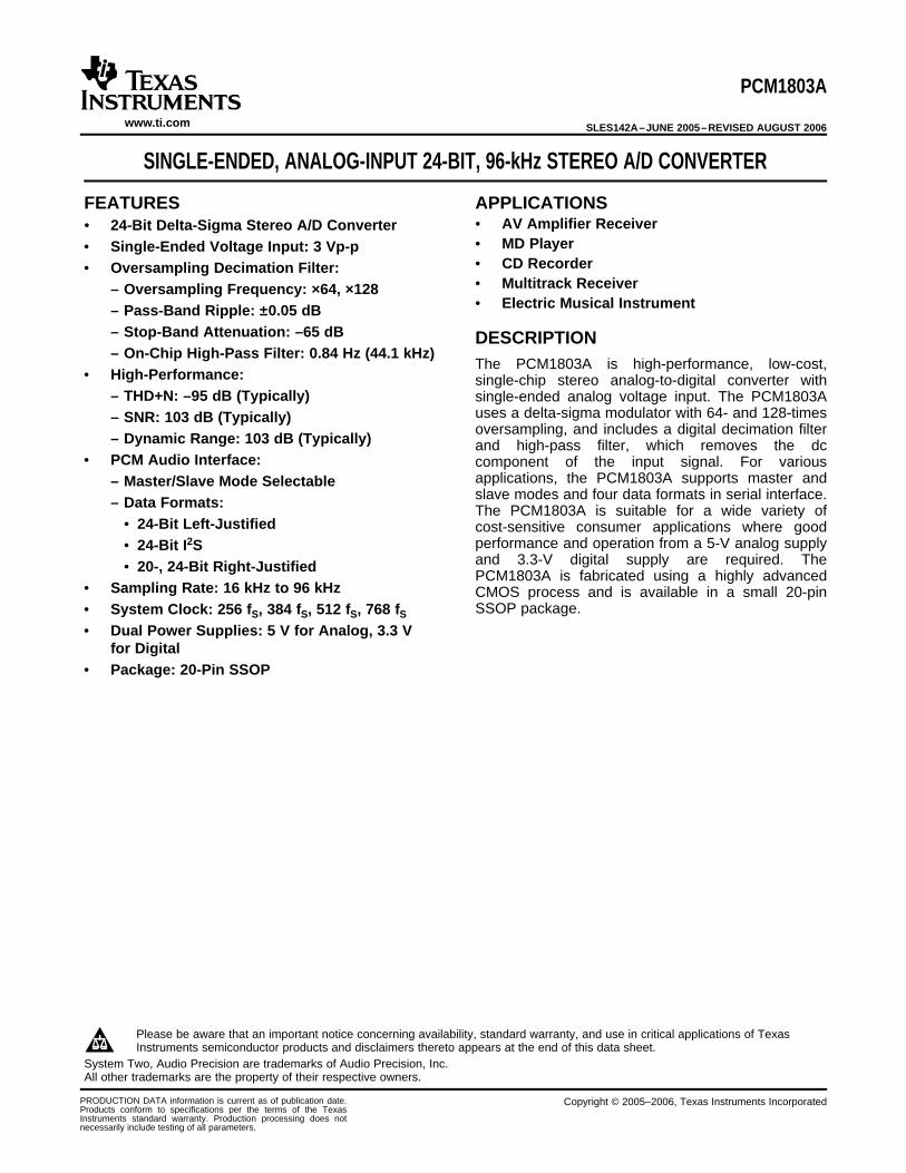
TYPICAL PERFORMANCE CURVES OF INTERNAL FILTER
Decimation Filter Frequency Response
Normalized Frequency [ × fS]
−200
−150
−100
−50
0
50
0 8 16 24 32 40 48 56 64
Oversampling Ratio = 128
Am
plitu
de −
dB
G001 G002Normalized Frequency [ × fS]
−200
−150
−100
−50
0
50
0 8 16 24 32
Am
plitu
de −
dB
Oversampling Ratio = 64
G003Normalized Frequency [ × fS]
−100
−90
−80
−70
−60
−50
−40
−30
−20
−10
0
0.00 0.25 0.50 0.75 1.00
Am
plitu
de −
dB
OversamplingRatio = 128 and 64
G004Normalized Frequency [ × fS]
−1.0
−0.8
−0.6
−0.4
−0.2
0.0
0.2
0.0 0.1 0.2 0.3 0.4 0.5 0.6
Am
plitu
de −
dB
OversamplingRatio = 128 and 64
PCM1803A
SLES142A–JUNE 2005–REVISED AUGUST 2006
All specifications at TA = 25°C, VCC = 5 V, VDD = 3.3 V, master mode, fS = 44.1 kHz, system clock = 384 fS,oversampling ratio = ×128, 24-bit data (unless otherwise noted)
OVERALL CHARACTERISTICS OVERALL CHARACTERISTICS
Figure 1. Figure 2.
STOP-BAND ATTENUATION CHARACTERISTICS PASS-BAND RIPPLE CHARACTERISTICS
Figure 3. Figure 4.
6 Submit Documentation Feedback

www.ti.com
LOW-CUT FILTER FREQUENCY RESPONSE
G005Normalized Frequency [ × fS/1000]
−100
−90
−80
−70
−60
−50
−40
−30
−20
−10
0
0.0 0.1 0.2 0.3 0.4
Am
plitu
de −
dB
G006Normalized Frequency [ × fS/1000]
−1.0
−0.8
−0.6
−0.4
−0.2
0.0
0.2
0 1 2 3 4
Am
plitu
de −
dB
PCM1803A
SLES142A–JUNE 2005–REVISED AUGUST 2006
TYPICAL PERFORMANCE CURVES OF INTERNAL FILTER (continued)All specifications at TA = 25°C, VCC = 5 V, VDD = 3.3 V, master mode, fS = 44.1 kHz, system clock = 384 fS,oversampling ratio = ×128, 24-bit data (unless otherwise noted)
HPF STOP-BAND CHARACTERISTICS HPF PASS-BAND CHARACTERISTICS
Figure 5. Figure 6.
7Submit Documentation Feedback

www.ti.com
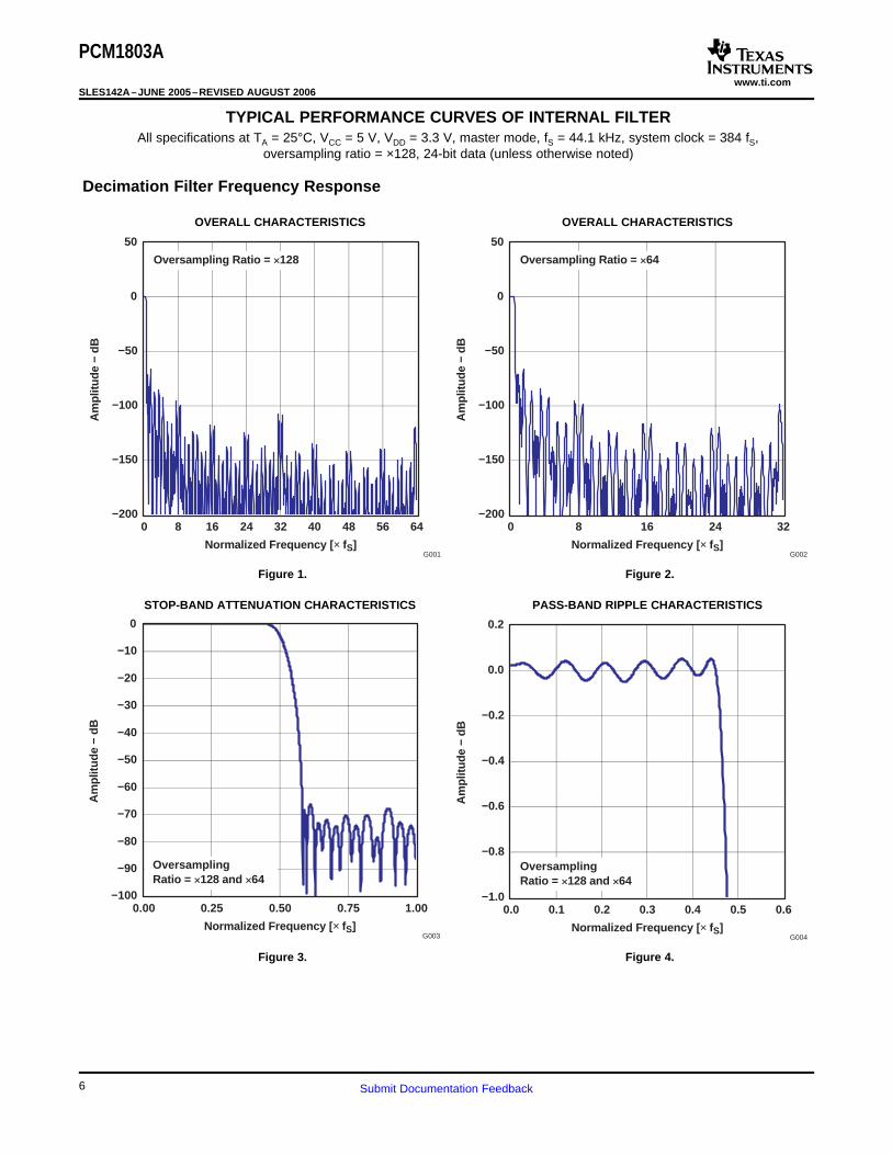
TYPICAL PERFORMANCE CURVES
G007
−100
−99
−98
−97
−96
−95
−94
−93
−92
−91
−90
−50 −25 0 25 50 75 100
TA − Free-Air T emperature − °C
TH
D+N
− T
otal
Har
mon
ic D
isto
rtion
+ N
oise
− d
B
100
101
102
103
104
105
106
107
108
109
110
−50 −25 0 25 50 75 100
G008TA − Free-Air T emperature − °C
Dyn
amic
Ran
ge a
nd S
NR
− d
B
SNR
Dynamic Range
−100
−99
−98
−97
−96
−95
−94
−93
−92
−91
−90
4.25 4.50 4.75 5.00 5.25 5.50 5.75
VCC − Supply V oltage − V
TH
D+N
− T
otal
Har
mon
ic D
isto
rtion
+ N
oise
− d
B
G009 G010
100
101
102
103
104
105
106
107
108
109
110
4.25 4.50 4.75 5.00 5.25 5.50 5.75
VCC − Supply V oltage − V
Dyn
amic
Ran
ge a
nd S
NR
− d
B
SNR
Dynamic Range
PCM1803A
SLES142A–JUNE 2005–REVISED AUGUST 2006
All specifications at TA = 25°C, VCC = 5 V, VDD = 3.3 V, master mode, fS = 44.1 kHz, system clock = 384 fS,oversampling ratio = ×128, 24-bit data (unless otherwise noted)
TOTAL HARMONIC DISTORTION + NOISE DYNAMIC RANGE and SIGNAL-TO-NOISE RATIOvs vs
TEMPERATURE TEMPERATURE
Figure 7. Figure 8.
TOTAL HARMONIC DISTORTION + NOISE DYNAMIC RANGE and SIGNAL-TO-NOISE RATIOvs vs
SUPPLY VOLTAGE SUPPLY VOLTAGE
Figure 9. Figure 10.
8 Submit Documentation Feedback
www.ti.com
−100
−99
−98
−97
−96
−95
−94
−93
−92
−91
−90
0 10 20 30 40
fSAMPLE Condition − kHz
TH
D+N
− T
otal
Har
mon
ic D
isto
rtion
+ N
oise
− d
B
44.1 96(2)48(1)
(1)fS = 48 kHz, System Clock = 256 f S, Oversampling Ratio = ×128.(2)fS = 96 kHz, System Clock = 256 f S, Oversampling Ratio = ×64.
G011
100
101
102
103
104
105
106
107
108
109
110
0 10 20 30 40
Dyn
amic
Ran
ge a
nd S
NR
− d
B
44.1 96(2)48(1)
SNR
Dynamic Range
fSAMPLE Condition − kHz
(1)fS = 48 kHz, System Clock = 256 f S, Oversampling Ratio = ×128.(2)fS = 96 kHz, System Clock = 256 f S, Oversampling Ratio = ×64.
G012
OUTPUT SPECTRUM
G013f − Frequency − kHz
−140
−120
−100
−80
−60
−40
−20
0
0 5 10 15 20
Input Level = −0.5 dBData Points = 8192
Am
plitu
de −
dB
G014
f − Frequency − kHz
−140
−120
−100
−80
−60
−40
−20
0
0 5 10 15 20
Am
plitu
de −
dB
Input Level = −60 dBData Points = 8192
PCM1803A
SLES142A–JUNE 2005–REVISED AUGUST 2006
TYPICAL PERFORMANCE CURVES (continued)All specifications at TA = 25°C, VCC = 5 V, VDD = 3.3 V, master mode, fS = 44.1 kHz, system clock = 384 fS,oversampling ratio = ×128, 24-bit data (unless otherwise noted)
TOTAL HARMONIC DISTORTION + NOISE DYNAMIC RANGE and SIGNAL-TO-NOISE RATIOvs vs
fSAMPLE CONDITION fSAMPLE CONDITION
Figure 11. Figure 12.
OUTPUT SPECTRUM OUTPUT SPECTRUM
Figure 13. Figure 14.
9Submit Documentation Feedback
www.ti.com
−100
−90
−80
−70
−60
−50
−40
−30
−20
−10
0
−100 −90 −80 −70 −60 −50 −40 −30 −20 −10 0
Signal Level − dB
TH
D+N
− T
otal
Har
mon
ic D
isto
rtion
+ N
oise
− d
B
G015
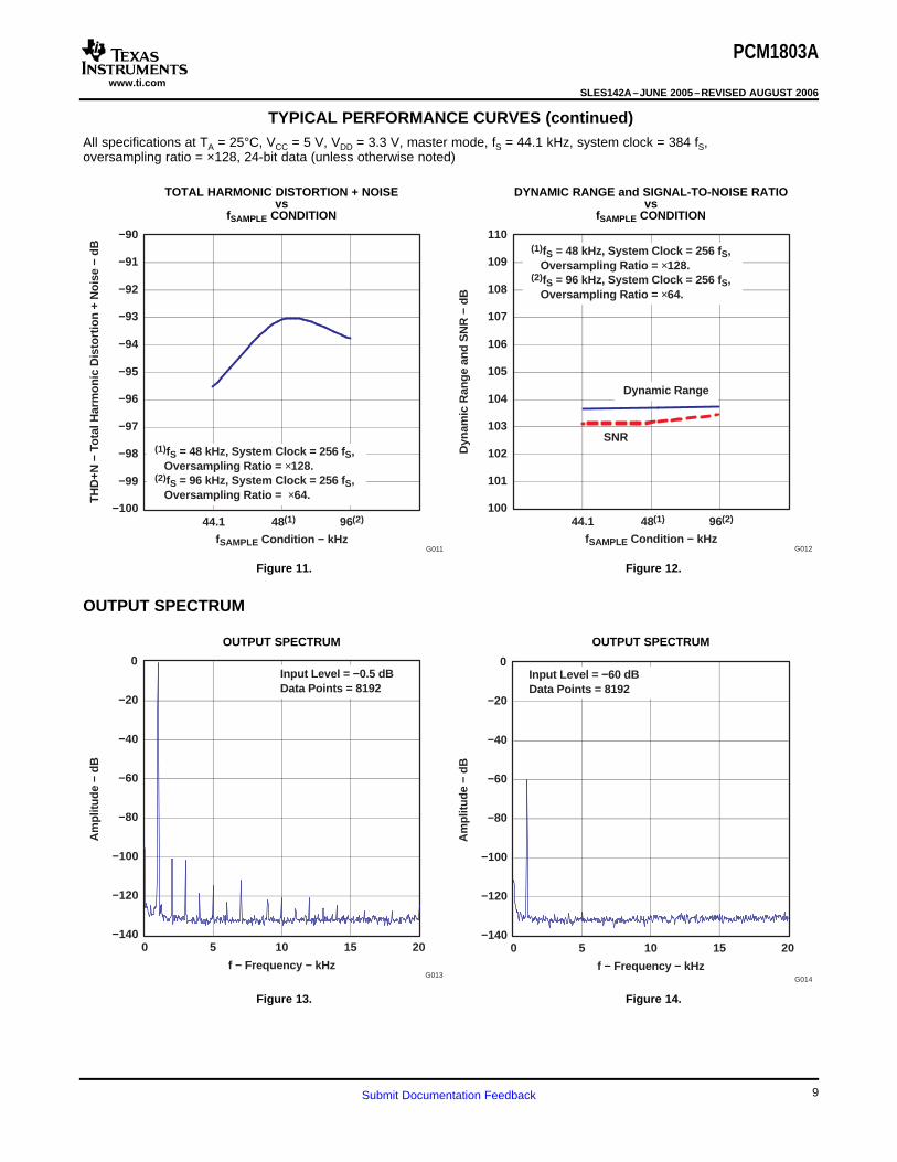
SUPPLY CURRENT
0
5
10
15
0 10 20 30 40
I CC
and
ID
D −
Sup
ply
Cur
rent
− m
A
44.1 96(2)48(1)
ICC
fSAMPLE Condition − kHz
IDD
(1)fS = 48 kHz, System Clock = 256 f S, Oversampling Ratio = ×128.(2)fS = 96 kHz, System Clock = 256 f S, Oversampling Ratio = ×64.
G016
PCM1803A
SLES142A–JUNE 2005–REVISED AUGUST 2006
TYPICAL PERFORMANCE CURVES (continued)All specifications at TA = 25°C, VCC = 5 V, VDD = 3.3 V, master mode, fS = 44.1 kHz, system clock = 384 fS,oversampling ratio = ×128, 24-bit data (unless otherwise noted)
TOTAL HARMONIC DISTORTION + NOISEvs
SIGNAL LEVEL
Figure 15.
SUPPLY CURRENTvs
fSAMPLE CONDITION
Figure 16.
10 Submit Documentation Feedback

www.ti.com
DEVICE INFORMATION
SYSTEM CLOCK
SCKI0.8 V
SCKI
2 V
tw(SCKL)tw(SCKH)
T0005B07
POWER-ON-RESET SEQUENCE
PCM1803A
SLES142A–JUNE 2005–REVISED AUGUST 2006
The PCM1803A supports 256 fS, 384 fS, 512 fS, and 768 fS as the system clock, where fS is the audio samplingfrequency. The system clock must be supplied on SCKI (pin 15).
The PCM1803A has a system clock-detection circuit that automatically senses if the system clock is operating at256 fS, 384 fS, 512 fS, or 768 fS in slave mode. In master mode, the system clock frequency must be selected byMODE0 (pin 19) and MODE1 (pin 20), and 768 fS is not available. The system clock is divided automatically into128 fS and 64 fS, and these frequencies are used to operate the digital filter and the delta-sigma modulator.
Table 1 shows the relationship of typical sampling frequency and system clock frequency, and Figure 17 showssystem clock timing.
Table 1. Sampling Frequency and System Clock Frequency
SYSTEM CLOCK FREQUENCY (MHz)SAMPLING FREQUENCY (kHz)
256 fS 384 fS 512 fS 768 fS(1)
32 8.1920 12.2880 16.3840 24.5760
44.1 11.2896 16.9344 22.5792 33.8688
48 12.2880 18.4320 24.5760 36.8640
64 16.3840 24.5760 32.7680 49.1520
88.2 22.5792 33.8688 45.1584 –
96 24.5760 36.8640 49.1520 –
(1) Slave mode only
SYMBOL PARAMETER MIN MAX UNIT
tw(SCKH) System clock pulse duration, HIGH 8 ns
tw(SCKL) System clock pulse duration, LOW 8 ns
Figure 17. System Clock Timing
The PCM1803A has an internal power-on-reset circuit, and initialization (reset) is performed automatically at thetime when power-supply voltage (VDD) exceeds 2.2 V (typical). While VDD < 2.2 V (typical) and for 1024 systemclock cycles after VDD > 2.2 V (typical), the PCM1803A stays in the reset state, and the digital output is forced tozero. The digital output becomes valid when a time period of 4480/fS has elapsed following release from thereset state. Figure 18 illustrates the internal power-on-reset timing and the digital output for power-on reset.
11Submit Documentation Feedback

www.ti.com
System Clock
2.6 V 2.2 V 1.8 V
Internal Reset
DOUT Zero Data Normal Data
Reset
VDD
Reset Removal
1024 System Clocks 4480 / fS
T0014-05
SERIAL AUDIO DATA INTERFACE
INTERFACE MODE
DATA FORMAT
PCM1803A
SLES142A–JUNE 2005–REVISED AUGUST 2006
Figure 18. Internal Power-On-Reset Timing
The PCM1803A interfaces the audio system through BCK (pin 11), LRCK (pin 10), and DOUT (pin 12).
The PCM1803A supports master mode and slave mode as interface modes, and they are selected by MODE1(pin 20) and MODE0 (pin 19) as shown in Table 2.
In master mode, the PCM1803A provides the timing of serial audio data communications between thePCM1803A and the digital audio processor or external circuit. While in slave mode, the PCM1803A receives thetiming for data transfers from an external controller.
Table 2. Interface Mode
MODE1 MODE0 INTERFACE MODE
0 0 Slave mode (256 fS, 384 fS, 512 fS, 768 fS)
0 1 Master mode (512 fS)
1 0 Master mode (384 fS)
1 1 Master mode (256 fS)
Master Mode
In master mode, BCK and LRCK work as output pins, and these pins are controlled by timing, which isgenerated in the clock circuit of the PCM1803A. The frequency of BCK is fixed at LRCK × 64. The 768-fS systemclock is not available in master mode.
Slave Mode
In slave mode, BCK and LRCK work as input pins. The PCM1803A accepts the 64-BCK/LRCK or 48-BCK/LRCKformat (only for 384 fS and 768 fS system clocks), not the 32-BCK/LRCK format.
The PCM1803A supports four audio data formats in both master and slave modes, and the data formats areselected by FMT1 (pin 18) and FMT0 (pin 17) as shown in Table 3. Figure 19 illustrates the data formats inslave and master modes.
12 Submit Documentation Feedback

www.ti.com
LRCK Right-ChannelLeft-Channel
BCK
DOUT 24 22 23 24321
MSB LSB
22 23 24321
MSB LSB
LRCK Right-ChannelLeft-Channel
BCK
DOUT 20 18 19 20321
MSB LSB
18 19 20321
MSB LSB
LRCK Right-ChannelLeft-Channel
BCK
DOUT 22 23 24321
MSB LSB
22 23 24321
MSB LSB
BCK
LRCK Right-ChannelLeft-Channel
DOUT 122 23 24321
MSB LSB
22 23 24321
MSB LSB
24-Bit, MSB-First, Left-Justified
FORMAT 0: FMT[1:0] = 00
24-Bit, MSB-First, I 2S
FORMAT 1: FMT[1:0] = 01
24-Bit, MSB-First, Right-Justified
FORMAT 2: FMT[1:0] = 10
20-Bit, MSB-First, Right-Justified
FORMAT 3: FMT[1:0] = 1 1
T0016-11
PCM1803A
SLES142A–JUNE 2005–REVISED AUGUST 2006
Table 3. Data Formats
FORMAT FMT1 FMT0 DESCRIPTION
0 0 0 Left-justified, 24-bit
1 0 1 I2S, 24-bit
2 1 0 Right-justified, 24-bit
3 1 1 Right-justified, 20-bit
Figure 19. Audio Data Formats (LRCK and BCK Work as Inputs in Slave Mode and as Outputs in MasterMode)
13Submit Documentation Feedback

www.ti.com
INTERFACE TIMING
BCK
LRCK
DOUT
t(BCKH)
t(BCKL)
t(LRHD)
t(LRCP)
t(LRSU)
t(BCKP) t(CKDO) t(LRDO)
1.4 V
1.4 V
0.5 VDD
T0017-02
PCM1803A
SLES142A–JUNE 2005–REVISED AUGUST 2006
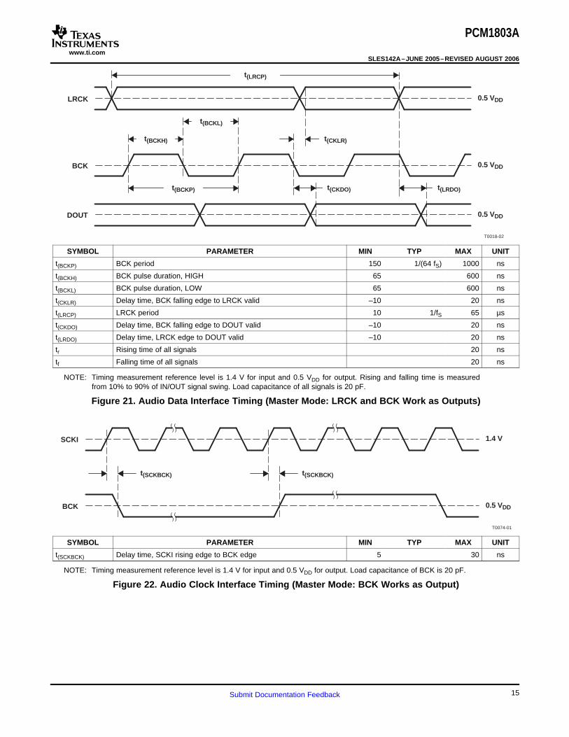
Figure 20 illustrates the interface timing in slave mode; Figure 21 and Figure 22 illustrate the interface timing inmaster mode.
SYMBOL PARAMETER MIN TYP MAX UNIT
t(BCKP) BCK period 1/(64 fS) ns
t(BCKH) BCK pulse duration, HIGH 1.5 × t(SCKI) ns
t(BCKL) BCK pulse duration, LOW 1.5 × t(SCKI) ns
t(LRSU) LRCK setup time to BCK rising edge 40 ns
t(LRHD) LRCK hold time to BCK rising edge 20 ns
t(LRCP) LRCK period 10 µs
t(CKDO) Delay time, BCK falling edge to DOUT valid –10 40 ns
t(LRDO) Delay time, LRCK edge to DOUT valid –10 40 ns
tr Rising time of all signals 20 ns
tf Falling time of all signals 20 ns
NOTE: Timing measurement reference level is 1.4 V for input and 0.5 VDD for output. Rising and falling time is measuredfrom 10% to 90% of IN/OUT signal swing. Load capacitance of DOUT is 20 pF. t(SCKI) means SCKI period time.
Figure 20. Audio Data Interface Timing (Slave Mode: LRCK and BCK Work as Inputs)
14 Submit Documentation Feedback
www.ti.com
BCK
LRCK
DOUT
t(BCKH)
t(BCKL)
t(CKLR)
t(LRCP)
t(BCKP) t(CKDO) t(LRDO)
0.5 VDD
0.5 VDD
0.5 VDD
T0018-02
BCK
SCKI
t(SCKBCK)
1.4 V
0.5 VDD
T0074-01
t(SCKBCK)
PCM1803A
SLES142A–JUNE 2005–REVISED AUGUST 2006
SYMBOL PARAMETER MIN TYP MAX UNIT
t(BCKP) BCK period 150 1/(64 fS) 1000 ns
t(BCKH) BCK pulse duration, HIGH 65 600 ns
t(BCKL) BCK pulse duration, LOW 65 600 ns
t(CKLR) Delay time, BCK falling edge to LRCK valid –10 20 ns
t(LRCP) LRCK period 10 1/fS 65 µs
t(CKDO) Delay time, BCK falling edge to DOUT valid –10 20 ns
t(LRDO) Delay time, LRCK edge to DOUT valid –10 20 ns
tr Rising time of all signals 20 ns
tf Falling time of all signals 20 ns
NOTE: Timing measurement reference level is 1.4 V for input and 0.5 VDD for output. Rising and falling time is measuredfrom 10% to 90% of IN/OUT signal swing. Load capacitance of all signals is 20 pF.
Figure 21. Audio Data Interface Timing (Master Mode: LRCK and BCK Work as Outputs)
SYMBOL PARAMETER MIN TYP MAX UNIT
t(SCKBCK) Delay time, SCKI rising edge to BCK edge 5 30 ns
NOTE: Timing measurement reference level is 1.4 V for input and 0.5 VDD for output. Load capacitance of BCK is 20 pF.
Figure 22. Audio Clock Interface Timing (Master Mode: BCK Works as Output)
15Submit Documentation Feedback

www.ti.com
SYNCHRONIZATION WITH DIGITAL AUDIO SYSTEM
1/fS 32/fS
NORMAL DATAZERO DATAUNDEFINED
DATANORMAL DATA
SYNCHRONOUSASYNCHRONOUSSYNCHRONOUS
ResynchronizationSynchronization Lost
DOUT
State of Synchronization
T0020-05
PCM1803A
SLES142A–JUNE 2005–REVISED AUGUST 2006
In slave mode, the PCM1803A operates under LRCK, synchronized with system clock SCKI. The PCM1803Adoes not need a specific phase relationship between LRCK and SCKI, but does require the synchronization ofLRCK and SCKI.
If the relationship between LRCK and SCKI changes more than ±6 BCKs for 64 BCK/frame (±5 BCKs for 48BCK/frame) during one sample period due to LRCK or SCKI jitter, internal operation of the ADC halts within 1/fS,and digital output is forced to zero data (BPZ code) until resynchronization between LRCK and SCKI occurs.
In case of changes less than ±5 BCKs for 64 BCK/frame (±4 BCKs for 48 BCK/frame), resynchronization doesnot occur and the previously explained digital output control and discontinuity do not occur.
Figure 23 illustrates the digital output response for loss of synchronization and resynchronization. Duringundefined data, the PCM1803A can generate some noise in the audio signal. Also, the transition of normal toundefined data and undefined or zero data to normal creates a discontinuity in the data of the digital output,which can generate some noise in the audio signal.
Figure 23. ADC Digital Output for Loss of Synchronization and Resynchronization
16 Submit Documentation Feedback

www.ti.com
POWER DOWN
HPF BYPASS
OVERSAMPLING RATIO CONTROL
PCM1803A
SLES142A–JUNE 2005–REVISED AUGUST 2006
PDWN (pin 7) controls operation of the entire ADC. During power-down mode, supply current for the analogportion is shut down and the digital portion is reset; also, DOUT (pin 12) is disabled. It is acceptable to halt thesystem clock during power-down mode so that power dissipation is minimized. The minimum LOW pulseduration on the PDWN pin is 100 ns.
It is recommended to set PWDN (pin 7) to LOW once to obtain stable analog performance when the samplingrate, interface mode, data format, or oversampling control is changed.
Table 4. Power-Down Control
PWDN Power-Down Mode
LOW Power-down mode
HIGH Normal operation mode
The built-in function for dc-component rejection can be bypassed by BYPAS (pin 8) control. In bypass mode, thedc component of the input analog signal, internal dc offset, etc., also are converted and included in the digitaloutput data.
Table 5. HPF Bypass Control
BYPAS HPF (High-Pass Filter) Mode
LOW Normal (no dc component in DOUT) mode
HIGH Bypass (dc component in DOUT) mode
OSR (pin 16) controls the oversampling ratio of the delta-sigma modulator, ×64 or ×128. The ×128 mode isavailable for fS ≤ 48 kHz.
Table 6. Oversampling Control
OSR Oversampling Ratio
LOW ×64
HIGH ×128 (fS ≤ 48 kHz)
17Submit Documentation Feedback

www.ti.com
APPLICATION INFORMATION
TYPICAL CIRCUIT CONNECTION DIAGRAM
VINL 20
19
18
17
16
15
14
13
12
11
1
2
3
4
5
6
7
8
9
10
PCM1803A
VINR
VREF1
VREF2
VCC
AGND
PDWN
BYPAS
TEST
LRCK
MODE1
DGND
MODE0
FMT1
FMT0
OSR
DOUT
BCK
VDD
SCKI
+ Oversampling
System Clock
L-Ch IN
R-Ch IN
+5 VC4
+C5
Power Down
LCF BypassControl
+ C3
L/R Clock
Audio DataProcessor
Mode [1:0]
Format [1:0]
+3.3 V
Data Clock
Data Out
+C1
+C2
Control
R1
S0026-03
+C6
R2
C7 C8
PCM1803A
SLES142A–JUNE 2005–REVISED AUGUST 2006
Figure 24 illustrates a typical circuit connection diagram where the cutoff frequency of the input HPF is about160 kHz.
NOTES:
A. C1, C2: A 1-µF electrolytic capacitor gives a 4-Hz (τ = 1 µF × 40 kΩ) cutoff frequency for the input HPF in normaloperation and requires a power-on settling time with a 40-ms time constant during the power-on initialization period.
B. C3, C4: Bypass capacitors are 0.1-µF ceramic and 10-µF electrolytic, depending on layout and power supply.
C. C5, C6: Recommended capacitors are 0.1-µF ceramic and 10-µF electrolytic.
D. C7, C8, R1, R2: A 0.01-µF film-type capacitor and 100-Ω resistor give a 160-kHz (τ = 0.01 µF × 100 Ω) cutofffrequency for the anti-aliasing filter in normal operation.
Figure 24. Typical Application Diagram
18 Submit Documentation Feedback

www.ti.com
BOARD DESIGN and LAYOUT CONSIDERATIONS
VCC, VDD Pins
AGND, DGND Pins
VINL, VINR Pins
VREF1 Pin
VREF2 Pin
DOUT Pin
System Clock
PCM1803A
SLES142A–JUNE 2005–REVISED AUGUST 2006
APPLICATION INFORMATION (continued)
The digital and analog power-supply lines to the PCM1803A should be bypassed to the corresponding groundpins with 0.1-µF ceramic and 10-µF electrolytic capacitors, as close to the pins as possible, to maximize thedynamic performance of the ADC.
To maximize the dynamic performance of the PCM1803A, the analog and digital grounds are not connectedinternally. These grounds should have low impedance to avoid digital noise feeding back into the analog ground.Therefore, they should be connected directly to each other under the part to reduce potential noise problems.
The VINL and VINR pins need a simple external RC filter (fC = 160 kHz) as an antialiasing filter to removeout-of-band noise from the audio band. If the input signal includes noise with a frequency near the oversamplingfrequency (64 fS or 128 fS), the noise is folded into the baseband (audio band) signal through A-to-D conversion.The recommended R value is 100 Ω. Film-type capacitors of 0.01-µF should be located as close as possible tothe VINL and VINR pins and should be terminated to GND as close as possible to the AGND pin to maximize thedynamic performance of ADC, by suppressing kickback noise from the PCM1803A.
A 0.1-µF ceramic capacitor and 10-µF electrolytic capacitor are recommended between VREF1 and AGND toensure low source impedance of the ADC references. These capacitors should be located as close as possibleto the VREF1 pin to reduce dynamic errors on the ADC reference.
The differential voltage between VREF2 and AGND sets the analog input full-scale range. A 0.1-µF ceramiccapacitor and 10-µF electrolytic capacitor are recommended between VREF2 and AGND. These capacitorsshould be located as close as possible to the VREF2 pin to reduce dynamic errors on the ADC reference.
The DOUT pin has enough load drive capability, but if the DOUT line is long, locating a buffer near thePCM1803A and minimizing load capacitance is recommended to minimize the digital-analog crosstalk andmaximize the dynamic performance of the ADC.
The quality of the system clock can influence the dynamic performance, because the PCM1803A operatesbased on a system clock. Therefore, it may be required to consider the system-clock duty, jitter, and the timedifference between system-clock transition and BCK or LRCK transition in the slave mode.
19Submit Documentation Feedback

PACKAGING INFORMATION
Orderable Device Status (1) PackageType
PackageDrawing
Pins PackageQty
Eco Plan (2) Lead/Ball Finish MSL Peak Temp (3)
PCM1803ADB ACTIVE SSOP DB 20 65 Green (RoHS &no Sb/Br)
CU NIPDAU Level-1-260C-UNLIM
PCM1803ADBG4 ACTIVE SSOP DB 20 65 Green (RoHS &no Sb/Br)
CU NIPDAU Level-1-260C-UNLIM
PCM1803ADBR ACTIVE SSOP DB 20 2000 Green (RoHS &no Sb/Br)
CU NIPDAU Level-1-260C-UNLIM
PCM1803ADBRG4 ACTIVE SSOP DB 20 2000 Green (RoHS &no Sb/Br)
CU NIPDAU Level-1-260C-UNLIM
(1) The marketing status values are defined as follows:ACTIVE: Product device recommended for new designs.LIFEBUY: TI has announced that the device will be discontinued, and a lifetime-buy period is in effect.NRND: Not recommended for new designs. Device is in production to support existing customers, but TI does not recommend using this part ina new design.PREVIEW: Device has been announced but is not in production. Samples may or may not be available.OBSOLETE: TI has discontinued the production of the device.
(2) Eco Plan - The planned eco-friendly classification: Pb-Free (RoHS), Pb-Free (RoHS Exempt), or Green (RoHS & no Sb/Br) - please checkhttp://www.ti.com/productcontent for the latest availability information and additional product content details.TBD: The Pb-Free/Green conversion plan has not been defined.Pb-Free (RoHS): TI's terms "Lead-Free" or "Pb-Free" mean semiconductor products that are compatible with the current RoHS requirementsfor all 6 substances, including the requirement that lead not exceed 0.1% by weight in homogeneous materials. Where designed to be solderedat high temperatures, TI Pb-Free products are suitable for use in specified lead-free processes.Pb-Free (RoHS Exempt): This component has a RoHS exemption for either 1) lead-based flip-chip solder bumps used between the die andpackage, or 2) lead-based die adhesive used between the die and leadframe. The component is otherwise considered Pb-Free (RoHScompatible) as defined above.Green (RoHS & no Sb/Br): TI defines "Green" to mean Pb-Free (RoHS compatible), and free of Bromine (Br) and Antimony (Sb) based flameretardants (Br or Sb do not exceed 0.1% by weight in homogeneous material)
(3) MSL, Peak Temp. -- The Moisture Sensitivity Level rating according to the JEDEC industry standard classifications, and peak soldertemperature.
Important Information and Disclaimer:The information provided on this page represents TI's knowledge and belief as of the date that it isprovided. TI bases its knowledge and belief on information provided by third parties, and makes no representation or warranty as to theaccuracy of such information. Efforts are underway to better integrate information from third parties. TI has taken and continues to takereasonable steps to provide representative and accurate information but may not have conducted destructive testing or chemical analysis onincoming materials and chemicals. TI and TI suppliers consider certain information to be proprietary, and thus CAS numbers and other limitedinformation may not be available for release.
In no event shall TI's liability arising out of such information exceed the total purchase price of the TI part(s) at issue in this document sold by TIto Customer on an annual basis.
PACKAGE OPTION ADDENDUM
www.ti.com 5-Jul-2006
Addendum-Page 1

TAPE AND REEL INFORMATION
*All dimensions are nominal
Device PackageType
PackageDrawing
Pins SPQ ReelDiameter
(mm)
ReelWidth
W1 (mm)
A0 (mm) B0 (mm) K0 (mm) P1(mm)
W(mm)
Pin1Quadrant
PCM1803ADBR SSOP DB 20 2000 330.0 17.4 8.5 7.6 2.4 12.0 16.0 Q1
PACKAGE MATERIALS INFORMATION
www.ti.com 24-Nov-2008
Pack Materials-Page 1

*All dimensions are nominal
Device Package Type Package Drawing Pins SPQ Length (mm) Width (mm) Height (mm)
PCM1803ADBR SSOP DB 20 2000 336.6 336.6 28.6
PACKAGE MATERIALS INFORMATION
www.ti.com 24-Nov-2008
Pack Materials-Page 2

MECHANICAL DATA
MSSO002E – JANUARY 1995 – REVISED DECEMBER 2001
POST OFFICE BOX 655303 • DALLAS, TEXAS 75265
DB (R-PDSO-G**) PLASTIC SMALL-OUTLINE
4040065 /E 12/01
28 PINS SHOWN
Gage Plane
8,207,40
0,550,95
0,25
38
12,90
12,30
28
10,50
24
8,50
Seating Plane
9,907,90
30
10,50
9,90
0,38
5,605,00
15
0,22
14
A
28
1
2016
6,506,50
14
0,05 MIN
5,905,90
DIM
A MAX
A MIN
PINS **
2,00 MAX
6,90
7,50
0,65 M0,15
0°–8°
0,10
0,090,25
NOTES: A. All linear dimensions are in millimeters.B. This drawing is subject to change without notice.C. Body dimensions do not include mold flash or protrusion not to exceed 0,15.D. Falls within JEDEC MO-150
IMPORTANT NOTICETexas Instruments Incorporated and its subsidiaries (TI) reserve the right to make corrections, modifications, enhancements, improvements,and other changes to its products and services at any time and to discontinue any product or service without notice. Customers shouldobtain the latest relevant information before placing orders and should verify that such information is current and complete. All products aresold subject to TI’s terms and conditions of sale supplied at the time of order acknowledgment.TI warrants performance of its hardware products to the specifications applicable at the time of sale in accordance with TI’s standardwarranty. Testing and other quality control techniques are used to the extent TI deems necessary to support this warranty. Except wheremandated by government requirements, testing of all parameters of each product is not necessarily performed.TI assumes no liability for applications assistance or customer product design. Customers are responsible for their products andapplications using TI components. To minimize the risks associated with customer products and applications, customers should provideadequate design and operating safeguards.TI does not warrant or represent that any license, either express or implied, is granted under any TI patent right, copyright, mask work right,or other TI intellectual property right relating to any combination, machine, or process in which TI products or services are used. Informationpublished by TI regarding third-party products or services does not constitute a license from TI to use such products or services or awarranty or endorsement thereof. Use of such information may require a license from a third party under the patents or other intellectualproperty of the third party, or a license from TI under the patents or other intellectual property of TI.Reproduction of TI information in TI data books or data sheets is permissible only if reproduction is without alteration and is accompaniedby all associated warranties, conditions, limitations, and notices. Reproduction of this information with alteration is an unfair and deceptivebusiness practice. TI is not responsible or liable for such altered documentation. Information of third parties may be subject to additionalrestrictions.Resale of TI products or services with statements different from or beyond the parameters stated by TI for that product or service voids allexpress and any implied warranties for the associated TI product or service and is an unfair and deceptive business practice. TI is notresponsible or liable for any such statements.TI products are not authorized for use in safety-critical applications (such as life support) where a failure of the TI product would reasonablybe expected to cause severe personal injury or death, unless officers of the parties have executed an agreement specifically governingsuch use. Buyers represent that they have all necessary expertise in the safety and regulatory ramifications of their applications, andacknowledge and agree that they are solely responsible for all legal, regulatory and safety-related requirements concerning their productsand any use of TI products in such safety-critical applications, notwithstanding any applications-related information or support that may beprovided by TI. Further, Buyers must fully indemnify TI and its representatives against any damages arising out of the use of TI products insuch safety-critical applications.TI products are neither designed nor intended for use in military/aerospace applications or environments unless the TI products arespecifically designated by TI as military-grade or "enhanced plastic." Only products designated by TI as military-grade meet militaryspecifications. Buyers acknowledge and agree that any such use of TI products which TI has not designated as military-grade is solely atthe Buyer's risk, and that they are solely responsible for compliance with all legal and regulatory requirements in connection with such use.TI products are neither designed nor intended for use in automotive applications or environments unless the specific TI products aredesignated by TI as compliant with ISO/TS 16949 requirements. Buyers acknowledge and agree that, if they use any non-designatedproducts in automotive applications, TI will not be responsible for any failure to meet such requirements.Following are URLs where you can obtain information on other Texas Instruments products and application solutions:Products ApplicationsAmplifiers amplifier.ti.com Audio www.ti.com/audioData Converters dataconverter.ti.com Automotive www.ti.com/automotiveDLP® Products www.dlp.com Broadband www.ti.com/broadbandDSP dsp.ti.com Digital Control www.ti.com/digitalcontrolClocks and Timers www.ti.com/clocks Medical www.ti.com/medicalInterface interface.ti.com Military www.ti.com/militaryLogic logic.ti.com Optical Networking www.ti.com/opticalnetworkPower Mgmt power.ti.com Security www.ti.com/securityMicrocontrollers microcontroller.ti.com Telephony www.ti.com/telephonyRFID www.ti-rfid.com Video & Imaging www.ti.com/videoRF/IF and ZigBee® Solutions www.ti.com/lprf Wireless www.ti.com/wireless
Mailing Address: Texas Instruments, Post Office Box 655303, Dallas, Texas 75265Copyright © 2009, Texas Instruments Incorporated