16v 3a 4-switch buck-boost charging/discharging converter … · 2018-06-30 · 16v 3a 4-switch...
TRANSCRIPT

EC3653
E-CMOS Corp. (www.ecmos.com.tw) 7I11N-Rev. F001
16V 3A 4-Switch Buck-Boost Charging/Discharging Converter
1/12
General Description The EC3653 is a buck boost converter targets HVDC fast charging and discharging power bank. The EC3653 supports 1 to 3 cells Li-ion battery, the output voltage can be programmable up to 16.0V through external resistor. The EC3653 implements the Buck Boost converter with an H-bridge, which can maintain output regulation for Input voltage whether greater or less than output voltage. The integrated low Rds(on) MOSFET minimizes physical footprint, maximizes charge/discharge efficiency, which reduces the power dissipation during discharge. Constant current control is utilized to protect the device from overshooting in unwanted conditions. Built-in loop compensation simplifies the circuit and design. PFM is engaged to maintain high efficiency at light load current. EC3653 guarantees robustness with thermal protection and battery under voltage lockout.
Features ◆Integrate low RDS (on) power MOSFET
◆Wide input range: 4.2V-16.0V, Support 1 to 3
◆cells battery charge/discharge.
◆Wide output range:0.9V-16.0V
◆High efficiency buck-boost transition
◆500kHz Switching frequency
◆Programmable output current limit(up to 3A)
◆Output Constant Current Control.
◆Quiescent current: <50uA
◆Integrate output overvoltage protection and
◆output short protection
◆Integrate thermal protection
◆QFN3*4 package
Applications
◆Power bank systems
◆Battery and Super Capacitor Charging
◆USB Power Delivery
◆Industrial applications
◆Automotive Systems Typical application

EC3653
E-CMOS Corp. (www.ecmos.com.tw) 7I11N-Rev. F001
16V 3A 4-Switch Buck-Boost Charging/Discharging Converter
2/12
Ordering/Marking Information
EC3653 XX X X
R:Tape & Reel
Package Type: F:Pb Free
Q4=QFN3*4-15L G:Green
Pin Configurations
Absolute Maximum Ratings VBUS,BAT, SW1, SW2 Pin .................................................................................................... -0.3Vto 20V BST1-SW1, BST2-SW2 ......................................................................................................... -0.3Vto 6.5V All Other Pins.......................................................................................................................... -0.3Vto 6.5V JunctionTemperature2)3) ....................................................................................................... 150ºC Lead Temperature .................................................................................................................. 260ºC Storage Temperature............................................................................................................... -65ºC to +150ºC ESD Susceptibility (Human Body Model) ............................................................................... 2Kv
Recommended Operating Conditions
BUS Voltage VBUS.................................................................................................................. 0.9Vto 16V Battery Voltage VBAT............................................................................................................... 3.0Vto 16V
Thermal Performance Operation Junction Temp (TJ)................................................................................................. -40ºCto +125ºC QFN3X4-15............................................................................................................................. 48 11ºC/W
Device Marking Package Shipping
EC3653Q4XR QFN3*4-15L

EC3653
E-CMOS Corp. (www.ecmos.com.tw) 7I11N-Rev. F001
16V 3A 4-Switch Buck-Boost Charging/Discharging Converter
3/12
Note 1) Exceeding these ratings may damage the device. 2) The EC3653 guarantees robust performance from -40°Cto 150°C junction temperature. The junction temperature range specification is assured by design, characterization and correlation with statistical process controls. 3) The EC3653 includes thermal protection that is intended to protect the device in overload conditions. Thermal protection is active when junction temperature exceeds the maximum operating junction temperature. Continuous operation over the specified absolute maximum operating junction temperature may damage the device. 4) Measured on JESD51-7, 4-layer PCB.

EC3653
E-CMOS Corp. (www.ecmos.com.tw) 7I11N-Rev. F001
16V 3A 4-Switch Buck-Boost Charging/Discharging Converter
4/12
Electrical Characteristics VBUS=12V, TA=25 , unless otherwise stated
Item Symbol Condition Min. Typ. Max. Units
Power supply
VBAT voltage range VBAT 3.0 16 V
VCC output voltage VCC IVCC=2mA 4.85 4.9 4.95 V
VCC output current limit IVCC VCC>2.7V 40 50 60 mA
Supply current in shut-down mode IQ VBAT=8V, EN=0V 40 50 60 µA
Controller
Switch frequency Fsw 450 500 550 kHz
Switch minimum off time Toff_min 80 100 120 ns
DE/STAT, CE/OLIM Logic HIGH VENH VBAT=8V 2.0 V
DE/STAT, CE/OLIM Logic LOW VENL VBAT=8V 0.4 V
Bucktop switch on-resistance RdsbkTG 20 28 m
Buck bottom switchon-resistance RdsbkBG 20 28 m
Boost top switch on-resistance RdsbstTG 20 28 m
Boost bottom switch on-resistance RdsbstBG 20 28 m
Charge
Floating BAT Voltage VCV
VBATFB =GND, EC3653
8.358 8.4 8.442 V
VBATFB =GND, EC3653-1
8.656 8.7 8.743 V
VBATFB = VCC, EC3653
12.53 12.6 12.67 V
VBATFB = VCC, EC3653-1
12.98 13.05 13.12 V
Set by divider resistance
3.0 - 16 V
BAT feedback voltage VBATFB External resistor divider 1.188 1.2 1.212 V
BAT Recharge threshold VREC VBATFB = GND 7.95 8.0 8.05 V
VBATFB = VCC 11.25 12.0 12.12 V
BAT recharge feedback threshold VRECFB 1.136 1.143 1.15 V
CC mode charge current ICC RCS=10m , RISET1=2K RISET2=1.5K
1.8 2 2.2 A
Charge termination current ITER RCS=10m , RISET1=2K RISET2=1.5K
200 mA
Battery full charge deglitch time TFULL ICC< ITER 25 s

EC3653
E-CMOS Corp. (www.ecmos.com.tw) 7I11N-Rev. F001
16V 3A 4-Switch Buck-Boost Charging/Discharging Converter
5/12
Trickle mode charge current ITRI RCS=10m , RISET1=2K RISET2=1.5K
200 mA
Trickle mode battery threshold VTRI Referred to one battery cell 3.0 V
Trickle charge time-out duration TTRI 50 55 60 min
VBUS UVP threshold VBUS_UVP VBUS increasing 3.98 4.1 4.22 V
VBUS decreasing 3.7 3.85 4 V
VBUS delay to start charging tchg_delay 150 ms
Initial charge current ICHG_ini 300 mA
Charge current increase step ISTEP1 75 100 125 mA
Charge current increase period tSTEP1 20 25 30 ms
VBUS droop voltage to foldback charge current
VDRP R1*3.8 µA
R1*4 µA
R1*4.2µA
V
Charge current limit decline step ISTEP2 100 mA
Charge current limit decline period tSTEP2 2.25 2.5 2.75 s
Discharge mode
VBAT UVLO voltage VBAT_UVLO
VBAT increasing 2.97 3.0 3.03 V
VBAT decreasing 2.54 2.6 2.66 V
Feedback voltage VFB 0.800 0.9 0.910 V
OLIM pin output current sense ratio KOLIM RCS=10m , RISET1=2K RISET2=1.5K
2.7 3 3.3 µA/A
OLIM pin regulate voltage VOLIM 390 400 410 mV
Output average current limit IO_LIM
RCS=10m , RISET1=2K RISET2=1.5K ROLIM=26K
1.8 2 2.2 A
Protection
VBUS OVP threshold VBUS_OVP
VBUS increasing 23.2 V
VBUS decreasing 21.5 V
VBUS OVP deglitch time tBUS_OVP
1.8 2 2.2 µs
VBAT OVP threshold VBAT_OVP
VBUS increasing 23.2 V
VBUS decreasing 21.5 V
VBAT OVP deglitch time tBAT_OVP 1.8 2 2.2 µs
Thermal shutdown threshold5) TSHUT 150 °C
Thermal recovery threshold5) TREC 130 °C
Notes: 5) Guaranteed by design.

EC3653
E-CMOS Corp. (www.ecmos.com.tw) 7I11N-Rev. F001
16V 3A 4-Switch Buck-Boost Charging/Discharging Converter
6/12
Pin Description Pin No. Name Description
1 CSP Positive terminal of battery charge current sense.
2 BAT Battery positive terminal.
3 PGND Power Ground.
4 VBUS In charge mode, main supply pin, connect to adaptor. In discharge mode, output voltage sense pin, connect this pin to Vout.
5 DRP/FB In charge mode, VBUS droop allowance program pin. In discharge mode, Output feedback pin.
6 CE/OLIM
Charge Enable control pin or Discharge output current limit program pin. This is a dual purpose Pin. When the CE/OLIM pin rises above 2.0V, the IC charge is enabled. When the charge is not used, in discharge mode, the pin set output average current limit. Connect a resistor to GND to set the maximum average current. And in the light load, it could be output current detection pin.
7 DE/STAT
Discharge Enable control pin or Fault state output pin or Charge state detection output pin. This is also a multi-purpose Pin. When the DE/STAT pin is above 2.0V and the CE/OLIM pin below 1.7V, the IC discharge is enabled. When the discharge is not used, in charge mode, the pin as Fault state output pin, asserted during over temperature or VBUS over voltage or trickle charge time out conditions. And the pin also as charge state detection output pin. In the CC charge mode, the pin source current is 6µA. In the full charge mode, the pin is pulled to high.
8 BST1 VBUS side bootstrap supply pin for top switch. 0.1µF capacitor is connected between BST1 and SW1 pins.
9 SW1 VBUS side power switching node. connect to SW1 with inductor
10 SW2 BAT side power switching node.
11 BST2 BAT side bootstrap supply pin for top switch. 0.1µF capacitor is connected between BST2 and SW2 pins.
12 BATFB
Battery float voltage configuration pin. 1. This pin tied to GND or VCC, sets different float voltage. Pin short to GND: 8.4V/8.7V. Pin short to VCC:12.6V/13.05V. 2. And the float voltage could be set to any value (3.0V-16.0V) by the external divider resistor.
13 VCC 4.9V LDO for power driver and internal circuit. Must be bypassed to GND with a minimum of 10µF ceramic capacitor for stable operation.
14 GND Signal GND.
15 CSN Negative terminal of battery charge current sense.
Notes: Highlighted pins are high current pins

EC3653
E-CMOS Corp. (www.ecmos.com.tw) 7I11N-Rev. F001
16V 3A 4-Switch Buck-Boost Charging/Discharging Converter
7/12
Block Diagram Typical Performance Characteristics Vin = 5V, L = 3.3µH, CIN = 140µF, CBAT=40uF, 2 Cells, TA = +25°C, unless otherwise noted.
EC3653
E-CMOS Corp. (www.ecmos.com.tw) 7I11N-Rev. F001
16V 3A 4-Switch Buck-Boost Charging/Discharging Converter
8/12
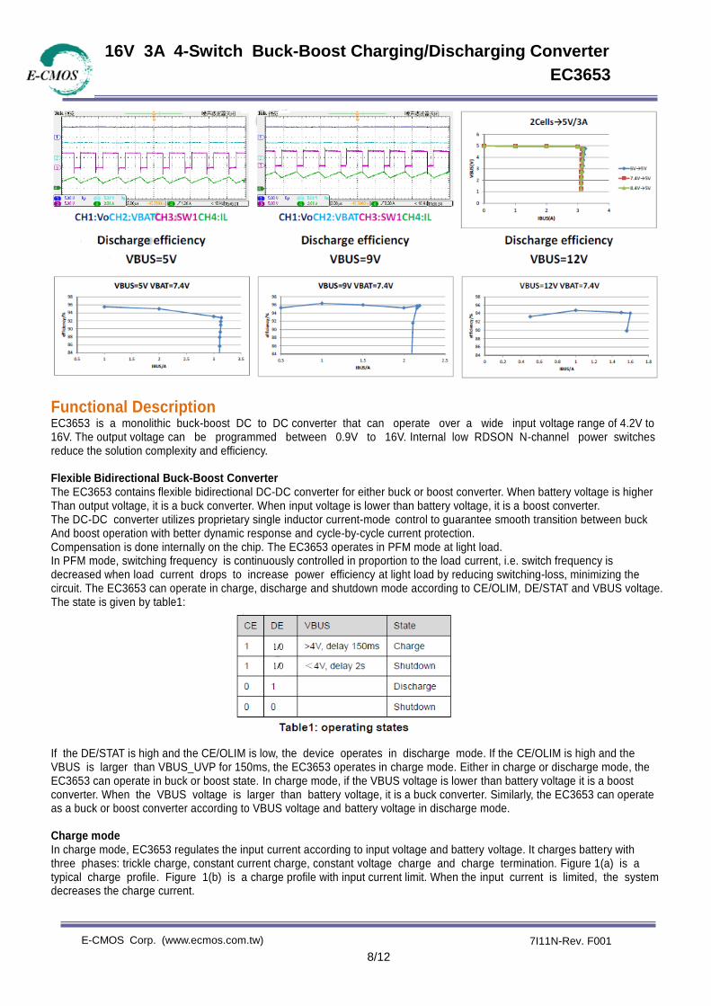
Functional Description EC3653 is a monolithic buck-boost DC to DC converter that can operate over a wide input voltage range of 4.2V to 16V. The output voltage can be programmed between 0.9V to 16V. Internal low RDSON N-channel power switches reduce the solution complexity and efficiency. Flexible Bidirectional Buck-Boost Converter The EC3653 contains flexible bidirectional DC-DC converter for either buck or boost converter. When battery voltage is higher Than output voltage, it is a buck converter. When input voltage is lower than battery voltage, it is a boost converter. The DC-DC converter utilizes proprietary single inductor current-mode control to guarantee smooth transition between buck And boost operation with better dynamic response and cycle-by-cycle current protection. Compensation is done internally on the chip. The EC3653 operates in PFM mode at light load. In PFM mode, switching frequency is continuously controlled in proportion to the load current, i.e. switch frequency is decreased when load current drops to increase power efficiency at light load by reducing switching-loss, minimizing the circuit. The EC3653 can operate in charge, discharge and shutdown mode according to CE/OLIM, DE/STAT and VBUS voltage. The state is given by table1: If the DE/STAT is high and the CE/OLIM is low, the device operates in discharge mode. If the CE/OLIM is high and the VBUS is larger than VBUS_UVP for 150ms, the EC3653 operates in charge mode. Either in charge or discharge mode, the EC3653 can operate in buck or boost state. In charge mode, if the VBUS voltage is lower than battery voltage it is a boost converter. When the VBUS voltage is larger than battery voltage, it is a buck converter. Similarly, the EC3653 can operate as a buck or boost converter according to VBUS voltage and battery voltage in discharge mode. Charge mode In charge mode, EC3653 regulates the input current according to input voltage and battery voltage. It charges battery with three phases: trickle charge, constant current charge, constant voltage charge and charge termination. Figure 1(a) is a typical charge profile. Figure 1(b) is a charge profile with input current limit. When the input current is limited, the system decreases the charge current.

EC3653
E-CMOS Corp. (www.ecmos.com.tw) 7I11N-Rev. F001
16V 3A 4-Switch Buck-Boost Charging/Discharging Converter
9/12
Trickle charge The EC3653 charges the battery with ITRI when battery voltage is less than VTRI. If charging remains in TC mode beyond the trickle-charge time TTRI, charging terminates. And meanwhile the DE/STAT pin will send out continuous clock signals with 20kHz switching frequency to inform MCU the fault state. CC charge When the battery is higher than VTRI, the device charges the battery with ICC if the input current is sufficient. When input current limit is hit, the device reduces the charge current automatically. In charge mode, the VBUS current is monitored continuously through CSP and CSN pins. As shown in Figure2, the external resistors RISET and RCS program the charge current. The maximum charging current is up to 3.4A.In the CC charging mode, the charging current is given by: And in the CC charge mode, a source current 2µA will be sent to DE/STAT pin to inform MCU the charge state conveniently.

EC3653
E-CMOS Corp. (www.ecmos.com.tw) 7I11N-Rev. F001
16V 3A 4-Switch Buck-Boost Charging/Discharging Converter
10/12
CV charge When battery voltage equals to VCV, the device regulates the battery voltage and reduces the charge current automatically. The customer can select 2 or 3 cells or program the VCV through BATFB pin. Connect BATFB to GND selects 2 cells. Connect BATFB to VCC selects 3 cells. The VCV also can be programmed by resistor divider connected to BATFB when the EC3653 detects a resistor connected to this pin. Charge termination If the battery voltage is higher than VFULL, and the charge current is less than charge termination current ITER for TFULL, the charge process terminates, and the DE/STAT pin is pulled to high. Auto recharge Once the battery charge cycle completes, the charger remains off. A new charge cycle automatically begins when the battery voltage falls below the auto-recharge threshold VREC if the input adaptor is present. The idle mode to charge mode transition also restarts the charge cycle. Dynamic input Current Tracking Scheme When the adaptor is plugged in for 150ms, the EC3653 starts charging with a limited charging current, in the meanwhile, the adaptor voltage is detected and stored as initial input voltage. Then the EC3653 increases charge current step by step. During this process, VBUS is continuously monitored. As long as VBUS drops preset level ( VDRP) below VBUS initial voltage, the system step by step lower the input current limit to bring back VBUS100mV higher to maintain a healthy adaptor output. After that the new input current limit is locked up unless the adaptor is plugged out. This is proprietary dynamic input current tracking scheme. Discharge Mode In discharge mode, EC3653 regulates the output voltage and output current. Output current sensing The EC3653 senses the output current through CE/OLIM pin when the output current is less than IO_LIM. If the output current is larger than IO_LIM, the CE/OLIM output a fixed voltage 400mV, the output current limit can be programmed through the resistor on CE/OLIM pin. Battery UVLO When battery voltage decreases to VBAT_UVLO1, the discharging process is terminated. When the battery voltage recovers and is larger than VBAT_UVLO2, the EC3653 can re-discharge if the DE/STAT is still high. Output constant current control In discharge mode, the output voltage is regulated to setting value which can be programmed through FB pin.

EC3653
E-CMOS Corp. (www.ecmos.com.tw) 7I11N-Rev. F001
16V 3A 4-Switch Buck-Boost Charging/Discharging Converter
11/12
The output current limit can be programmed by ROLIM. If the output current equals to the IO_LIMIT, the output current loop begins to work, it turns down output voltage to limit the output power. When output is shorted to ground, the EC3653 works as a buck converter, the output current is continuously sensed and Limited to IO_LIMIT. When the output short is removed, the regulator comes into normal operation again. Thermal Control When the junction temperature of the EC3653 rises above 135°C, it begins to reduce the output power to prevent the Temperature from rising further. If the junction temperature of the EC3653 rises above 150°C, the discharging process stops. Shut-down Mode The EC3653 shuts down when voltage at CE/OLIM pin and DE/STAT pin is below 0.4V. The entire regulator is off. BST UVLO If the BST1-SW1 or BST2-SW2 voltage is lower than BST UVLO Voltage, the switch is turned off. Protection VBUS Over-Voltage Protection If the adaptor voltage exceeds the VBUS over-charge threshold VBUS_OVP for tBUS_OVP, charging process suspends and the device generates a fault flag. Battery Over-Voltage Protection If the battery voltage exceeds the battery over-charge threshold VBAT_OVP for tBAT_OVP, charging process suspends and the device generates a fault flag.

EC3653
E-CMOS Corp. (www.ecmos.com.tw) 7I11N-Rev. F001
16V 3A 4-Switch Buck-Boost Charging/Discharging Converter
12/12
Package Outline QFN3X4-15