18 may, 2005 - digi-keymedia.digikey.com/pdf/data sheets/panasonic resistors thermistors... · 18...
TRANSCRIPT
1 of 1
18 May, 2005
APPROVAL
Y.Sakaguchi
CHECK
S. Endoh
DESIGN
T.Shinriki
Note ;
CLASSIFICATION SPECIFICATIONS No.
SUBJECT PAGE
DATE
151S-ERTJ-KE18E
Multilayer Chip NTC Thermistors
10 type Individual Specification (EIA 0402)
Panasonic Electronic Devices Co., Ltd.
1. ScopeThis specification applies to Multilayer Chip NTC Thermistors 10type (EIA0402).
2. Style and Dimensions
3. Operating Temperature Range- 40 to + 125 °C
4. Explanation of Part Numbers
E R T J 0 E T 1 0 4 J
5. Capacitance Tolerance
Table 2
Part NumberNominal Zero-powerResistance(at 25 °C)
B Value(B25/50)
Rated MaximumPower Dissipation *
DissipationFactor **
ERTJ0ET104J 100 kΩ +/- 5 % 4500 K +/- 2 % 66 mW Generally 2 mW / °C
*The maximum value power dissipation which can be continuously applied to the thermistors at 25 °C.
**The factor which indicates the power required to raise the temperature of the thermistor element in the thermalequilibrium, by 1 °C with its self-heat dissipation .It is obtained by dividing the power consumption of the Thermistors by the increase of element temperature.
L
L1
L2
W T Table 1
Symbol Dimensions(mm)
L 1.0 +/- 0.1
W 0.50 +/- 0.05
T 0.50 +/- 0.05
L1,L2 0.25 +/- 0.15
Resistance ToleranceCode Tolerance
J +/- 5 %
Common Code
Packaging StyleCode Packaging Style
E φ180Reel Paper Taping 10000pcs./reel
Size Code B ValueCode
Resistance(R25)
1 of 6
31 May, 2004
Panasonic Electronic Devices Co., Ltd.
APPROVAL
Y.Sakaguti
CHECK
S.Endoh
DESIGN
T.Shinriki
Note ; 01 Apr, 2005 Change the company name. Previous : Matsushita Electronic Components Co., Ltd. New : Panasonic Electronic Devices Co., Ltd.
CLASSIFICATION SPECIFICATIONS No.
SUBJECT PAGE
DATE
151S-ERTJ-SG01E
Multilayer Chip NTC Thermistors
(Standard type) Common Specification
1. Information1- 1. Applicable laws and regulations
(1) Any ozone-depleting substances listed in the Montreal Protocol are not used in the manufacturing processes for parts andmaterials used in this product.
(2) PBB and PBDE are intentionally excluded from materials used in this product.(3) All the materials used in this product are registered materials under the Law Concerning Examination and Regulation of
Manufacture and Handling of Chemical Substances.(4) This product complies with the RoHS, DIRECTIVE 2002/95/EC on the Restriction of the use of certain Hazardous Substances
in electrical and electronic equipment.(5) This product is exported with export procedures under export related laws and regulations such as the Foreign Exchange and
Foreign Trade Law.
1- 2. Limitation in Applications This product was designed and manufactured for general-purpose electronic equipment such as household, office, information &
communication equipment. When the following applications, which are required higher reliability and safety because the trouble ormalfunction of this product may threaten the lives and/or properties, are examined, separate specifications suitable for the applica-tion should be exchanged.
・Aerospace / Aircraft equipment, Warning / Antitheft equipment, Medical equipment, Transport equipment (Motor vehicles,Trains, Ship and Vessel ), Highly public information processing equipment, Others equivalent to the above.
1- 3. Production factory(1) Panasonic Electronic Devices Hokkaido Co., Ltd.(2) Tianjin Matsushita Electronic Components Co., Ltd.(TMCOM)
2. Scope This specification applies common specification to Multilayer chip NTC Thermistors. If there is a difference between this common speci-fication and any individual specifications, priority shall be given to the individual specifications.
2- 1. This product shall be used for general-purpose electronic equipment such as audiovisual, household, office, information & commu-nication equipment.Unreasonable applications may accelerate performance deterioration or short/open circuits as failure modes affecting the life end.Adequate safety shall be ensured especially for product design required a high level of safety with the following considerations.
1) Previously examine how a single trouble in this product affects the end product.2) Design a protection circuit as Failsafe-design to avoid unsafe system resulting from a single trouble with this product.
2- 2. Whenever a doubt about safety arises from this product, immediately inform us for technical consultation without fail, please.
3. Part Number CodeERTJ 1 V A 101 J _
(1) (2) (3) (4) (5) (6) (7)
3- 1. Common Code (1)ERTJ : Multilayer Chip NTC Thermistors
3- 2. Size (2)Z: “06”Type (0201/EIA)0: “10”Type (0402/EIA)1: ”11”Type (0603/EIA)

2 of 6
31 May, 2004
CLASSIFICATION SPECIFICATIONS No.
SUBJECT PAGE
DATE
151S-ERTJ-SG01E
Multilayer Chip NTC Thermistors
(Standard type) Common Specification
Note ;
3- 3. Packing Style (3)Shown in Individual Specification
3- 4. B Value Code (4)
3- 5. Resistance (R25)The Resistance (R25) expressed in ohm and is identified by a three-digit number ;the first two digit represent significant figures and the last digit specifies the numberof zero to follow.
3- 6. Resistance ToleranceShown in Individual Specification
3- 7. Special Specification
4. Operating Temperature RangeShown in Individual Specification.
5. Performance The performance of the Thermistor and its test condition shall be specified in Table 2.
6. TestUnless otherwise specified, all test and measurements shall be made at a temperature of 1575%.If results obtained are doubted a further test should be carried out at a temperature of 25 +/-
7. StructureThe structure shall be in a monolithic form as shown in Fig. 1.
Fig. 1
N
(
(
Code Center of B Value
A 2701~2800K
G 3301~3400K
P 4001~4100K
R 4201~4300K
S 4301~4400K
T 4401~4500K
V 4701~4800K
(1)
(2)
(3)
(4)
(5)
Symbol (Ex.) Resistance (R25)(ohm)
102 1000103 10000104 100000
to 35 and at a relative humidity of 45 to
2 and a relative humidity of 60 to 70%.
Table 1
o. Name(1) Ceramics(2) Inner Electrode(Pd)
(3) SubstrateElectrode (Cu)
4) IntermediateElectrode (Ni)
5)
TerminalElectrode
ExternalElectrode (Sn)
3 of 6
31 May, 2004
CLASSIFICATION SPECIFICATIONS No.
SUBJECT PAGE
DATE
151S-ERTJ-SG01E
Multilayer Chip NTC Thermistors
(Standard type) Common Specification
Note ;
Table 2No. Contents Performance Test Method1 Appearance There shall be no defects which affect the life
and use.With a magnifying glass (3 times).
2 Dimensions Shown in Individual Specification. With slide calipers and a micrometer.
3 Zero-power Resistance(R25)
Shown in Individual Specification. Zero-power resistance shall be measured at ambienttemperature of 25+/-0.1deg.C with a electric powerless than 0.1mW suppressing self heat generation.
4 B Value Shown in Individual Specification. Zero-power resistance shall be measured at T1(deg.C)and T2(deg.C) respectively shall be measured.The B value is calc wing equation.
R1: ResisR2: Resis
5 MaximumPermissibleelectrical power
Shown in Individual Specification. The maxcontinuouThe maxcording toexceeds
6 Dissipation Factor Shown in Individual Specification. Solder thFig.2.The factothe tempein the thedissipatioIt is obtainThermistoTemperat
7 Adhesion (Electrode peeling strength)
The terminal electrode shall be free frompeeling or signs of peeling.
Solder thFig.2. andseconds.・Force
Material : Thicknes
(continue)
B=
Rat
ed
Load
(%)
1
*
* 06 ty
1.0
1/(T1+273.15)-1/(T2+273.15)
ln(R1)-ln(R2)
tance attance at
imum elesly at 25imum el the foll
25 deg.C
e specim
r which rature ormal equn .ed by dr by the ure
e specim apply fo
06(EIA 0others typ
Alumina board.s : 1.0mm
50%
00%
pe;.R0.3
ulated by follo
T1 T2ctric power which is possible to loaddeg.C shall be measured.ectric power should be derated ac-owing curve when the temperatures.
en to the testing board shown in
indicates the power required to raisef the thermistor elementilibrium, by 1deg.C with its self-heat
ividing the power consumption of theincrease of element
en to the testing board shown inrce in the arrow direction for 10+/-1
201)type ; 2N e ; 5N
board (95% min.) or glass epoxy
min.
75 12525
*R0.5
Sample PC board
4 of 6
31 May, 2004
CLASSIFICATION SPECIFICATIONS No.
SUBJECT PAGE
DATE
151S-ERTJ-SG01E
Multilayer Chip NTC Thermistors
(Standard type) Common Specification
Note ;
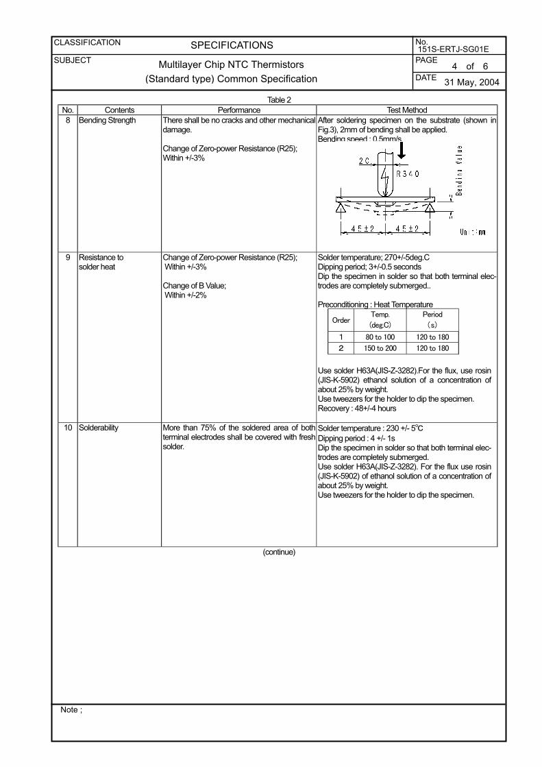
Table 2No. Contents Performance Test Method8 Bending Strength There shall be no cracks and other mechanical
damage.
Change of Zero-power Resistance (R25);Within +/-3%
After soldering specimen on the substrate (shown inFig.3), 2mm of bending shall be applied.Bending speed : 0.5mm/s
9 Resistance tosolder heat
Change of Zero-power Resistance (R25); Within +/-3%
Change of B Value; Within +/-2%
Solder temperature; 270+/-5deg.CDipping period; 3+/-0.5 secondsDip the specimen in solder so that both terminal elec-trodes are completely submerged..
Preconditioning : Heat Temperature
Us(JIabUsRe
10 Solderability More than 75% of the soldered area of bothterminal electrodes shall be covered with freshsolder.
SoDipDiptroUs(JIabUs
(continue)
OrderTemp.
(deg.C)
Period
(s)
1 80 to 100 120 to 180
2 150 to 200 120 to 180
e solder H63A(JIS-Z-3282).For the flux, use rosinS-K-5902) ethanol solution of a concentration ofout 25% by weight.e tweezers for the holder to dip the specimen.covery : 48+/-4 hours
lder temperature : 230 +/- 5ping period : 4 +/- 1s the specimen in solder so that both terminal elec-
des are completely submerged. e solder H63A(JIS-Z-3282). For the flux use rosinS-K-5902) of ethanol solution of a concentration ofout 25% by weight.e tweezers for the holder to dip the specimen.
5 of 6
31 May, 2004
CLASSIFICATION SPECIFICATIONS No.
SUBJECT PAGE
DATE
151S-ERTJ-SG01E
Multilayer Chip NTC Thermistors
(Standard type) Common Specification
Note ;
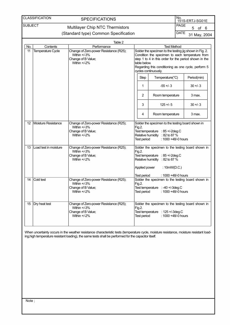
Table 2No. Contents Performance Test Method11 Temperature Cycle Change of Zero-power Resistance (R25);
Within +/-3%Change of B Value; Within +/-2%
Solder the specimen to the testing jig shown in Fig. 2.Condition the specimen to each temperature fromstep 1 to 4 in this order for the period shown in thetable below. Regarding this conditioning as one cycle, perform 5cycles continuously.
12 Moisture Resistance Change of Zero-power Resistance (R25); Within +/-3%Change of B Value; Within +/-2%
Solder the specimen to the testing board shown inFig.2.Test temperature : 85 +/-2deg.CRelative humidity : 82 to 87 %Test period : 1000 +48/-0 hours
13 Load test in moisture Change of Zero-power Resistance (R25); Within +/-3%Change of B Value; Within +/-2%
Solder the specimen to the testing board shown inFig.2.Test temperature : 85 +/-2deg.CRelative humidity : 82 to 87 %
Applied power : 10mW(D.C.)
Test period : 1000 +48/-0 hours14 Cold test Change of Zero-power Resistance (R25);
Within +/-3%Change of B Value; Within +/-2%
Solder the specimen to the testing board shown inFig.2.Test temperature : -40 +/-3deg.CTest period : 1000 +48/-0 hours
15 Dry heat test Change of Zero-power Resistance (R25); Within +/-3%Change of B Value; Within +/-2%
Solder the specimen to the testing board shown inFig.2.Test temperature : 125 +/-3deg.CTest period : 1000 +48/-0 hours
When uncertainty occurs in the weather resistance characteristic tests (temperature cycle, moisture resistance, moisture resistant load-ing,high temperature resistant loading), the same tests shall be performed for the capacitor itself.
Step Temperature(°C) Period(min)
1 -55 +/- 3 30 +/- 3
2 Room temperature 3 max.
3 125 +/- 5 30 +/- 3
4 Room temperature 3 max.
6 of 6
31 May, 2004
CLASSIFICATION SPECIFICATIONS No.
SUBJECT PAGE
DATE
151S-ERTJ-SG01E
Multilayer Chip NTC Thermistors
(Standard type) Common Specification
Note ;
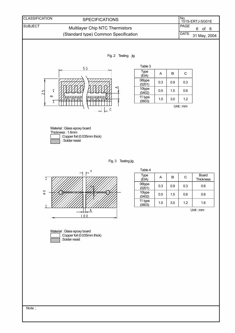
Fig. 2 Testing jig
Table 3
Type(EIA)
A B C
06type(0201)
0.3 0.9 0.3
10type(0402)
0.5 1.5 0.6
11 type(0603)
1.0 3.0 1.2
Unit : mm
Material : Glass epoxy boardThickness : 1.6mm
:Copper foil (0.035mm thick): Solder resist
Fig. 3 Testing jig
Table 4
Type(EIA)
A B CBoard
Thickness06type(0201)
0.3 0.9 0.3 0.6
10type(0402)
0.5 1.5 0.6 0.6
11 type(0603)
1.0 3.0 1.2 1.6
Unit : mm
Material : Glass epoxy board:Copper foil (0.035mm thick):Solder resist
1 of 831 May, 2004
APPROVAL
Y.Sakaguti
CHECK
S.Endoh
DESIGN
T.Shinriki
Note ; 01 Apr, 2005 Change the company name. Previous : Matsushita Electronic Components Co., Ltd. New : Panasonic Electronic Devices Co., Ltd.
CLASSIFICATION SPECIFICATIONS No.
SUBJECT PAGE
DATE
151S-ERTJ-SS01E
Multilayer Chip NTC ThermistorsCommon Specification ( Precautions for Use)
Panasonic Electronic Devices Co., Ltd.
1. Precautions for Use The Multilayer Chip NTC Thermistors (hereafter referred to as “Thermistors”) may fail in a short circuit mode or inan open circuit mode, when subjected to severe conditions of electrical environmental and / or mechanical stressbeyond the specified “Rating” and specified “Conditions” in the Specification, resulting in burnout, flaming orglowing in the worst case. Following “Precautions for Safety” and “Application Notes” shall be taken in your majorconsideration.
2. Operating Conditions and Circuit Design2- 1.Circuit Design
2-1-1. Operating Temperature Range The specified “Operating Temperature Range” in the Specifications is absolute maximum and minimumtemperature rating.So in any case, each of the Thermistors shall be operated within the specified “Operating Temperature Range”.
2-1-2. Operating Power The Thermistors shall not be operated beyond the specified Maximum Permissible Power (power rating shall bederated in accordance with the derating curve, if operated in ambient temperatures above 25 deg.C), otherwise,result in burn out and damages due to the thermal run away. The Thermistors may not be worked precisely astemperature detectors due to the own self heating, even if under the specified Maximum Permissible power. Takeinto account of the Heat Dissipation Constant and the Specified Maximum Permissible Power before use.
2-1-3. Restriction on Environmental ConditionsThe Thermistors shall not be operated and / or stored under the following environmental conditions.(1) Environmental conditions
(a) To be exposed directly to water or salt water(b) To be dew formation(c) Under conditions of corrosive gases such as hydrogen sulfide, sulfurous acid, chlorine and ammonia
(2) Under severe conditions of extreme vibrations or shocks.
2- 2.Design of Printed Circuit Board2-2-1. Selection of Printed Circuit Board
When the Thermistors are mounted and soldered on an Aluminum Substrate, the substrate has influences onThermistors reliabilities against “Temperature Cycles” and “Heat shock” because of difference in thermalexpansion coefficient between them.It shall be carefully confirmed that the actual board applied does not deteriorate the characteristics of theThermistors.
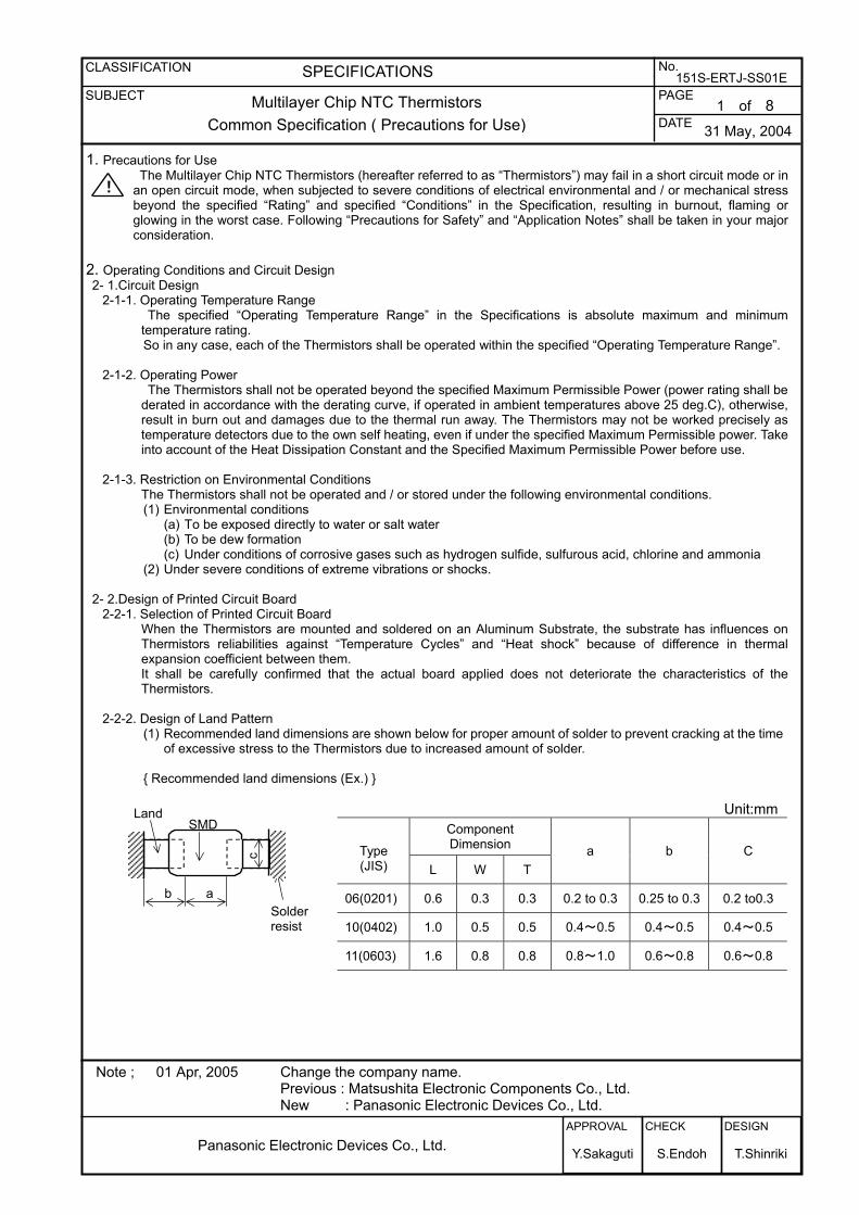
2-2-2. Design of Land Pattern(1) Recommended land dimensions are shown below for proper amount of solder to prevent cracking at the time
of excessive stress to the Thermistors due to increased amount of solder.
Recommended land dimensions (Ex.)
Unit:mmComponentDimensionType
(JIS) L W Ta b C
06(0201) 0.6 0.3 0.3 0.2 to 0.3 0.25 to 0.3 0.2 to0.3
10(0402) 1.0 0.5 0.5 0.4~0.5 0.4~0.5 0.4~0.5
11(0603) 1.6 0.8 0.8 0.8~1.0 0.6~0.8 0.6~0.8
!
abSolderresist
SMDLand
c
2 of 831 May, 2004
CLASSIFICATION SPECIFICATIONS No.
SUBJECT PAGE
DATE
151S-ERTJ-SS01E
Multilayer Chip NTC ThermistorsCommon Specification ( Precautions for Use)
Note ;
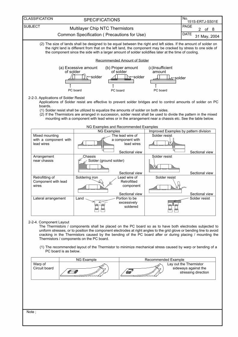
(2) The size of lands shall be designed to be equal between the right and left sides. If the amount of solder onthe right land is different from that on the left land, the component may be cracked by stress to one side ofthe component since the side with a larger amount of solder solidifies later at the time of cooling.
Recommended Amount of Solder
2-2-3. Applications of Solder ResistApplications of Solder resist are effective to prevent solder bridges and to control amounts of solder on PCboards.(1) Solder resist shall be utilized to equalize the amounts of solder on both sides.(2) If the Thermistors are arranged in succession, solder resist shall be used to divide the pattern in the mixed
mounting with a component with lead wires or in the arrangement near a chassis etc. See the table below.
NG Examples and Recommended ExamplesNG Examples Improved Examples by pattern division
Mixed mountingwith a component withlead wires
The lead wire of a component with lead wires
Sectional view
Solder resist
Sectional viewArrangementnear chassis
Chassis Solder (ground solder)
Sectional view
Solder resist
Sectional viewRetrofitting ofComponent with leadwires
Soldering iron Lead wire of Retrofitted component
Sectional view
Solder resist
Sectional viewLateral arrangement Land Portion to be
excessively soldered
Solder resist
2-2-4. Component LayoutThe Thermistors / components shall be placed on the PC board so as to have both electrodes subjected touniform stresses, or to position the component electrodes at right angles to the grid glove or bending line to avoidcracking in the Thermistors caused by the bending of the PC board after or during placing / mounting theThermistors / components on the PC board.
(1) The recommended layout of the Thermistor to minimize mechanical stress caused by warp or bending of aPC board is as below.
NG Example Recommended ExampleWarp ofCircuit board
Lay out the Thermistor sideways against the stressing direction
(a) Excessive amount of solder
(b) Proper amount of solder
(c)Insufficient amount
↑PC board
←solder
↑PC board
←solder
↑PC board
←solder
3 of 831 May, 2004
CLASSIFICATION SPECIFICATIONS No.
SUBJECT PAGE
DATE
151S-ERTJ-SS01E
Multilayer Chip NTC ThermistorsCommon Specification ( Precautions for Use)
Note ;
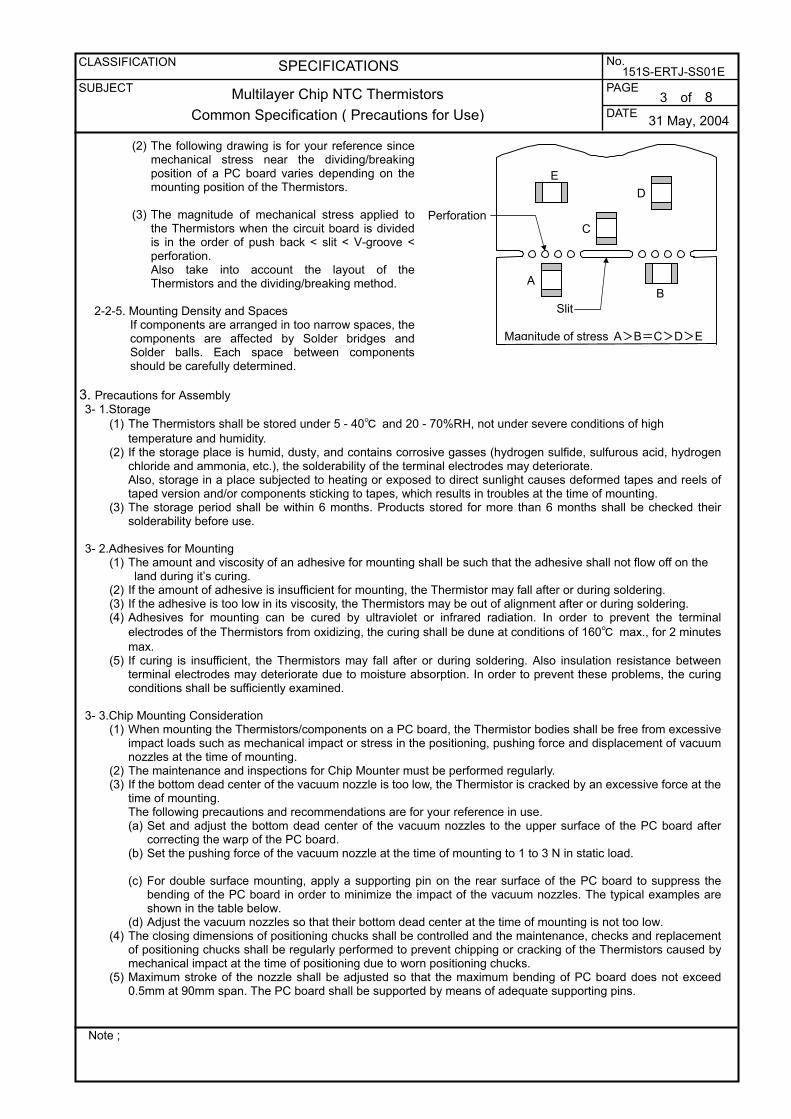
(2) The following drawing is for your reference sincemechanical stress near the dividing/breakingposition of a PC board varies depending on themounting position of the Thermistors.
(3) The magnitude of mechanical stress applied tothe Thermistors when the circuit board is dividedis in the order of push back < slit < V-groove <perforation.Also take into account the layout of theThermistors and the dividing/breaking method.
2-2-5. Mounting Density and SpacesIf components are arranged in too narrow spaces, thecomponents are affected by Solder bridges andSolder balls. Each space between componentsshould be carefully determined.
3. Precautions for Assembly3- 1.Storage
(1) The Thermistors shall be stored under 5 - 40 and 20 - 70%RH, not under severe conditions of hightemperature and humidity.
(2) If the storage place is humid, dusty, and contains corrosive gasses (hydrogen sulfide, sulfurous acid, hydrogenchloride and ammonia, etc.), the solderability of the terminal electrodes may deteriorate.Also, storage in a place subjected to heating or exposed to direct sunlight causes deformed tapes and reels oftaped version and/or components sticking to tapes, which results in troubles at the time of mounting.
(3) The storage period shall be within 6 months. Products stored for more than 6 months shall be checked theirsolderability before use.
3- 2.Adhesives for Mounting(1) The amount and viscosity of an adhesive for mounting shall be such that the adhesive shall not flow off on the
land during it’s curing.(2) If the amount of adhesive is insufficient for mounting, the Thermistor may fall after or during soldering.(3) If the adhesive is too low in its viscosity, the Thermistors may be out of alignment after or during soldering.(4) Adhesives for mounting can be cured by ultraviolet or infrared radiation. In order to prevent the terminal
electrodes of the Thermistors from oxidizing, the curing shall be dune at conditions of 160 max., for 2 minutesmax.
(5) If curing is insufficient, the Thermistors may fall after or during soldering. Also insulation resistance betweenterminal electrodes may deteriorate due to moisture absorption. In order to prevent these problems, the curingconditions shall be sufficiently examined.
3- 3.Chip Mounting Consideration(1) When mounting the Thermistors/components on a PC board, the Thermistor bodies shall be free from excessive
impact loads such as mechanical impact or stress in the positioning, pushing force and displacement of vacuumnozzles at the time of mounting.
(2) The maintenance and inspections for Chip Mounter must be performed regularly.(3) If the bottom dead center of the vacuum nozzle is too low, the Thermistor is cracked by an excessive force at the
time of mounting.The following precautions and recommendations are for your reference in use.(a) Set and adjust the bottom dead center of the vacuum nozzles to the upper surface of the PC board after
correcting the warp of the PC board.(b) Set the pushing force of the vacuum nozzle at the time of mounting to 1 to 3 N in static load.
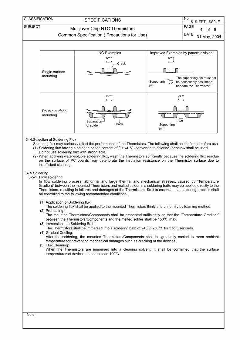
(c) For double surface mounting, apply a supporting pin on the rear surface of the PC board to suppress thebending of the PC board in order to minimize the impact of the vacuum nozzles. The typical examples areshown in the table below.
(d) Adjust the vacuum nozzles so that their bottom dead center at the time of mounting is not too low.(4) The closing dimensions of positioning chucks shall be controlled and the maintenance, checks and replacement
of positioning chucks shall be regularly performed to prevent chipping or cracking of the Thermistors caused bymechanical impact at the time of positioning due to worn positioning chucks.
(5) Maximum stroke of the nozzle shall be adjusted so that the maximum bending of PC board does not exceed0.5mm at 90mm span. The PC board shall be supported by means of adequate supporting pins.
AB
C
ED
Slit
Magnitude of stress A>B=C>D>E
Perforation
4 of 831 May, 2004
CLASSIFICATION SPECIFICATIONS No.
SUBJECT PAGE
DATE
151S-ERTJ-SS01E
Multilayer Chip NTC ThermistorsCommon Specification ( Precautions for Use)
Note ;
NG Examples Improved Examples by pattern division
Single surfacemounting
Double surfacemounting
3- 4.Selection of Soldering FluxSoldering flux may seriously affect the performance of the Thermistors. The following shall be confirmed before use.(1) Soldering flux having a halogen based content of 0.1 wt. % (converted to chlorine) or below shall be used.
Do not use soldering flux with strong acid.(2) When applying water-soluble soldering flux, wash the Thermistors sufficiently because the soldering flux residue
on the surface of PC boards may deteriorate the insulation resistance on the Thermistor surface due toinsufficient cleaning.
3- 5.Soldering3-5-1. Flow soldering
In flow soldering process, abnormal and large thermal and mechanical stresses, caused by ”TemperatureGradient" between the mounted Thermistors and melted solder in a soldering bath, may be applied directly to theThermistors, resulting in failures and damages of the Thermistors, So it is essential that soldering process shallbe controlled to the following recommended conditions.
(1) Application of Soldering flux:The soldering flux shall be applied to the mounted Thermistors thinly and uniformly by foaming method.
(2) Preheating:The mounted Thermistors/Components shall be preheated sufficiently so that the “Temperature Gradient”between the Thermistors/Components and the melted solder shall be 150 max.
(3) Immersion into Soldering Bath:The Thermistors shall be immersed into a soldering bath of 240 to 260 for 3 to 5 seconds.
(4) Gradual Cooling:After the soldering, the mounted Thermistors/Components shall be gradually cooled to room ambienttemperature for preventing mechanical damages such as cracking of the devices.
(5) Flux Cleaning:When the Thermistors are immersed into a cleaning solvent, it shall be confirmed that the surfacetemperatures of devices do not exceed 100.
Crack
Supportingpin
The supporting pin must notbe necessarily positionedbeneath the Thermistor.
Separationof solder Crack Supporting
pin
5 of 831 May, 2004
CLASSIFICATION SPECIFICATIONS No.
SUBJECT PAGE
DATE
151S-ERTJ-SS01E
Multilayer Chip NTC ThermistorsCommon Specification ( Precautions for Use)
Note ;
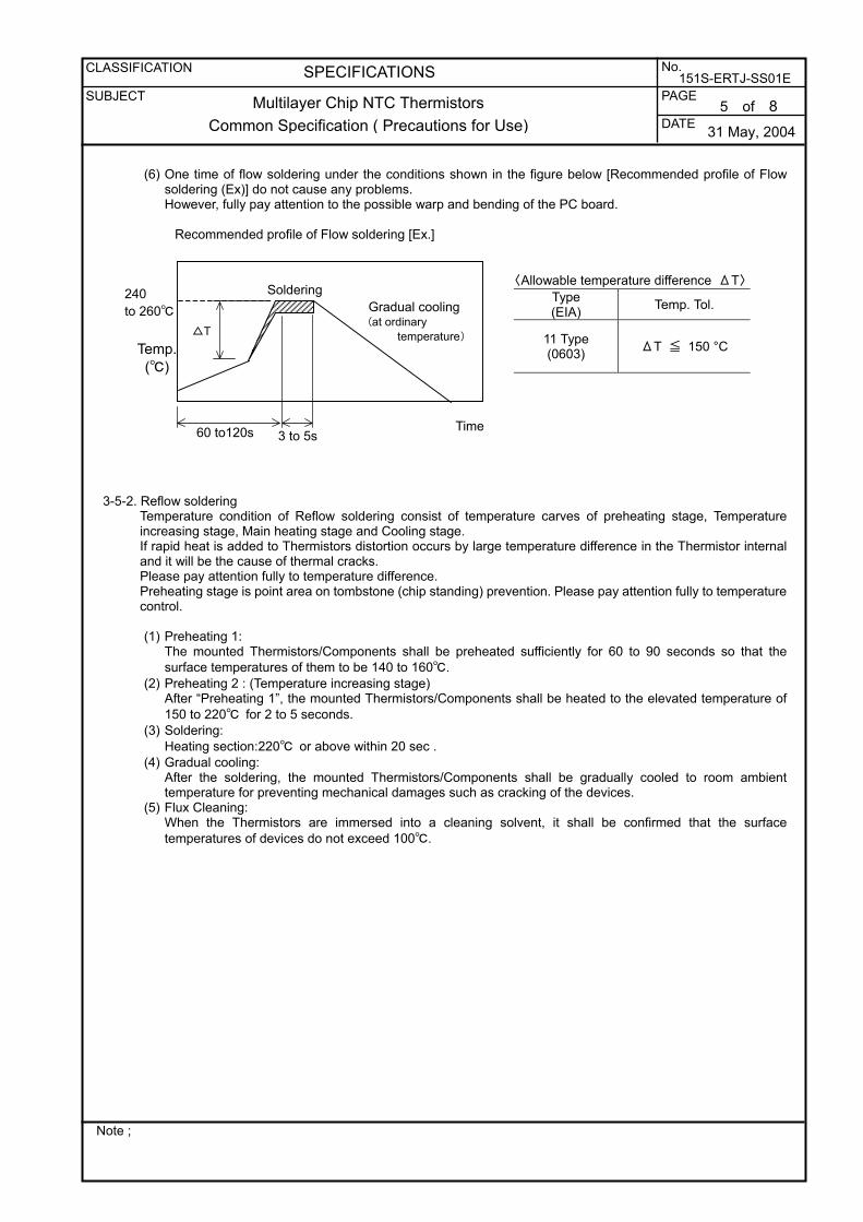
(6) One time of flow soldering under the conditions shown in the figure below [Recommended profile of Flowsoldering (Ex)] do not cause any problems.However, fully pay attention to the possible warp and bending of the PC board.
Recommended profile of Flow soldering [Ex.]
〈Allowable temperature difference ΔT〉
Type(EIA) Temp. Tol.
11 Type(0603) ΔT ≦ 150 °C
3-5-2. Reflow solderingTemperature condition of Reflow soldering consist of temperature carves of preheating stage, Temperatureincreasing stage, Main heating stage and Cooling stage.If rapid heat is added to Thermistors distortion occurs by large temperature difference in the Thermistor internaland it will be the cause of thermal cracks.Please pay attention fully to temperature difference.Preheating stage is point area on tombstone (chip standing) prevention. Please pay attention fully to temperaturecontrol.
(1) Preheating 1:The mounted Thermistors/Components shall be preheated sufficiently for 60 to 90 seconds so that thesurface temperatures of them to be 140 to 160.
(2) Preheating 2 : (Temperature increasing stage)After “Preheating 1”, the mounted Thermistors/Components shall be heated to the elevated temperature of150 to 220 for 2 to 5 seconds.
(3) Soldering:Heating section:220 or above within 20 sec .
(4) Gradual cooling:After the soldering, the mounted Thermistors/Components shall be gradually cooled to room ambienttemperature for preventing mechanical damages such as cracking of the devices.
(5) Flux Cleaning:When the Thermistors are immersed into a cleaning solvent, it shall be confirmed that the surfacetemperatures of devices do not exceed 100.
60 to120s 3 to 5s
SolderingGradual cooling(at ordinary temperature)T
240to 260
Time
Temp.()
6 of 831 May, 2004
CLASSIFICATION SPECIFICATIONS No.
SUBJECT PAGE
DATE
151S-ERTJ-SS01E
Multilayer Chip NTC ThermistorsCommon Specification ( Precautions for Use)
Note ;
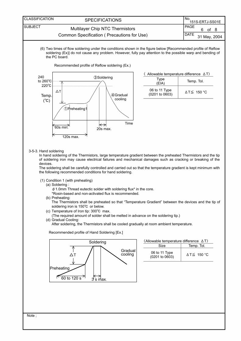
(6) Two times of flow soldering under the conditions shown in the figure below [Recommended profile of Reflowsoldering (Ex)] do not cause any problem. However, fully pay attention to the possible warp and bending ofthe PC board.
Recommended profile of Reflow soldering (Ex.)
〈 Allowable temperature difference ΔT〉
Type(EIA) Temp. Tol.
06 to 11 Type(0201 to 0603) ΔT≦ 150 °C
3-5-3. Hand solderingIn hand soldering of the Thermistors, large temperature gradient between the preheated Thermistors and the tipof soldering iron may cause electrical failures and mechanical damages such as cracking or breaking of thedevices.The soldering shall be carefully controlled and carried out so that the temperature gradient is kept minimum withthe following recommended conditions for hand soldering.
(1) Condition 1 (with preheating)(a) Soldering :
φ1.0mm Thread eutectic solder with soldering flux* in the core.*Rosin-based and non-activated flux is recommended.
(b) Preheating:The Thermistors shall be preheated so that “Temperature Gradient” between the devices and the tip ofsoldering iron is 150 or below.
(c) Temperature of Iron tip: 300 max.(The required amount of solder shall be melted in advance on the soldering tip.)
(d) Gradual Cooling:After soldering, the Thermistors shall be cooled gradually at room ambient temperature.
Recommended profile of Hand Soldering [Ex.]
〈Allowable temperature difference ΔT〉
Size Temp. Tol.
06 to 11 Type(0201 to 0603) ΔT≦ 150 °C
60 to 120 s
Soldering
Gradualcooling
Preheating
3 s max.
T
60s min.
①Preheating1
③Soldering
④Gradual cooling
Time
T
120s max.
20s max.
220
240to 260
Temp.()
7 of 831 May, 2004
CLASSIFICATION SPECIFICATIONS No.
SUBJECT PAGE
DATE
151S-ERTJ-SS01E
Multilayer Chip NTC ThermistorsCommon Specification ( Precautions for Use)
Note ;
(2) Condition 2 (without preheating)Modification with a soldering iron is acceptable without preheating if within the conditions specified below.(a) Soldering iron tip shall never directly touch the ceramic dielectrics and terminal electrodes of the
Thermistors.(b) The lands are sufficiently preheated with a soldering iron tip before sliding the soldering iron tip to the
terminal electrode of the Thermistor for soldering.
Conditions of Hand soldering without preheatingCondition
Temperature of soldering iron 270 °C Max.Wattage 20W Max.Shape of soldering iron tip φ3mm Max.Soldering time with soldering iron 3s Max.
3- 6.Post Soldering Cleaning3-6-1. Residues of soldering fluxes on the PC board after cleaning with an inappropriate solvent may deteriorate on the
electrical characteristics and reliability (particularly, insulation resistance) of the Thermistors.3-6-2. Inappropriate cleaning conditions (Such as insufficient cleaning, excessive cleaning) may impair the electrical
characteristics and reliability of the Thermistors.(1) If cleaning is insufficient :
(a) The halogen substance in the residues of the soldering flux may cause the metal of terminal electrodes tocorrode.
(b) The halogen substance in the residues of the soldering flux on the surface of the Thermistors maydeteriorate the insulation resistance.
(c) Water-soluble soldering flux may have more remarkable tendencies of (a) and (b) above compared tothose of rosin soldering flux.
(2) If cleaning is excessive :(a) Too much output of ultrasonic cleaning may deteriorate the strength of the terminal electrodes or cause
cracking in the solder and/or ceramic bodies of the Thermistors due to vibrated PC boards.The following conditions are for Ultrasonic cleaning.
Ultrasonic wave output: 20 W/L max. Ultrasonic wave frequency: 40 kHz max. Ultrasonic wave cleaning time: 5 min. max.
3-6-3. Cleaning with contaminated cleaning solvent may cause the same results in case of insufficient cleaning due tothe high density of liberated halogen.
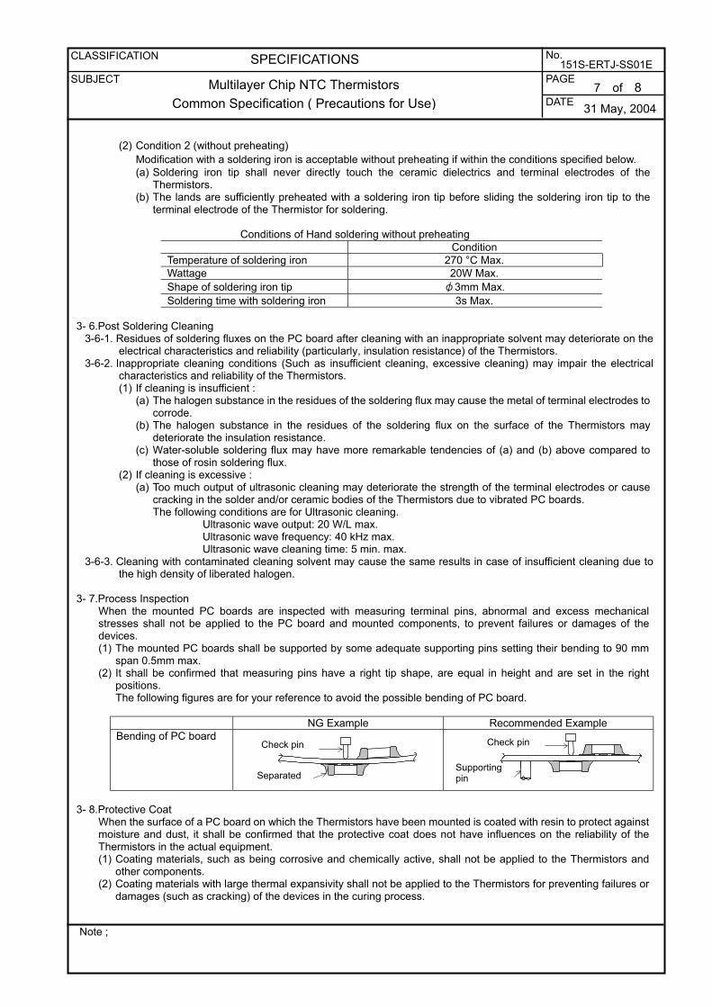
3- 7.Process InspectionWhen the mounted PC boards are inspected with measuring terminal pins, abnormal and excess mechanicalstresses shall not be applied to the PC board and mounted components, to prevent failures or damages of thedevices.(1) The mounted PC boards shall be supported by some adequate supporting pins setting their bending to 90 mm
span 0.5mm max.(2) It shall be confirmed that measuring pins have a right tip shape, are equal in height and are set in the right
positions.The following figures are for your reference to avoid the possible bending of PC board.
NG Example Recommended ExampleBending of PC board
3- 8.Protective CoatWhen the surface of a PC board on which the Thermistors have been mounted is coated with resin to protect againstmoisture and dust, it shall be confirmed that the protective coat does not have influences on the reliability of theThermistors in the actual equipment.(1) Coating materials, such as being corrosive and chemically active, shall not be applied to the Thermistors and
other components.(2) Coating materials with large thermal expansivity shall not be applied to the Thermistors for preventing failures or
damages (such as cracking) of the devices in the curing process.
Separated
Check pin
Supportingpin
Check pin
8 of 831 May, 2004
CLASSIFICATION SPECIFICATIONS No.
SUBJECT PAGE
DATE
151S-ERTJ-SS01E
Multilayer Chip NTC ThermistorsCommon Specification ( Precautions for Use)
Note ;
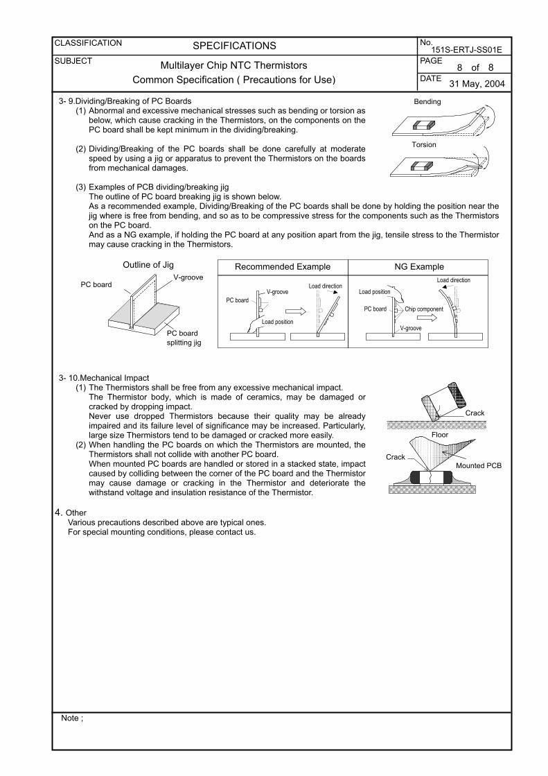
3- 9.Dividing/Breaking of PC Boards(1) Abnormal and excessive mechanical stresses such as bending or torsion as
below, which cause cracking in the Thermistors, on the components on thePC board shall be kept minimum in the dividing/breaking.
(2) Dividing/Breaking of the PC boards shall be done carefully at moderatespeed by using a jig or apparatus to prevent the Thermistors on the boardsfrom mechanical damages.
(3) Examples of PCB dividing/breaking jigThe outline of PC board breaking jig is shown below.As a recommended example, Dividing/Breaking of the PC boards shall be done by holding the position near thejig where is free from bending, and so as to be compressive stress for the components such as the Thermistorson the PC board.And as a NG example, if holding the PC board at any position apart from the jig, tensile stress to the Thermistormay cause cracking in the Thermistors.
3- 10.Mechanical Impact(1) The Thermistors shall be free from any excessive mechanical impact.
The Thermistor body, which is made of ceramics, may be damaged orcracked by dropping impact.Never use dropped Thermistors because their quality may be alreadyimpaired and its failure level of significance may be increased. Particularly,large size Thermistors tend to be damaged or cracked more easily.
(2) When handling the PC boards on which the Thermistors are mounted, theThermistors shall not collide with another PC board.When mounted PC boards are handled or stored in a stacked state, impactcaused by colliding between the corner of the PC board and the Thermistormay cause damage or cracking in the Thermistor and deteriorate thewithstand voltage and insulation resistance of the Thermistor.
4. OtherVarious precautions described above are typical ones.For special mounting conditions, please contact us.
Bending
Torsion
Recommended Example NG Example
PC boardsplitting jig
V-groovePC board
Outline of Jig
V-groove
Chip componentPC board
Load position
Load directionLoad position
PC board
V-groove
Load direction
Floor
Crack
Mounted PCBCrack
1 of 4
15 Jun, 2004
Panasonic Electronic Devices Co., Ltd.APPROVAL
Y.Sakaguti
CHECK
S.Endoh
DESIGN
T.Shinriki
Note ; 01 Apr, 2005 Change the company name. Previous : Matsushita Electronic Components Co., Ltd. New : Panasonic Electronic Devices Co., Ltd.
CLASSFICATION SPECIFICATIONS No.
SUBJECT PAGE
DATE
151S-ECJ-SV01E
Multilayer Chip NTC ThermistorsTaped and Reeled Packaging Specifications
1. ScopeThis specification applies to taped and reeled packing for Multilayer chip NTC Thermistors.
2. Applicable StandardsEIAJ (Electric Industries Association of Japan) Standard EIAJ RC-1009BJIS (Japanese Industrial Standard) Standard JIS C 0806
3. Packing Specification3- 1.Structure and Dimensions
Paper taping packaging is carried out according the following diagram1) Carrier tape : Shown in Fig. 4., Fig5.2) Reel : Shown in Fig.6.3) Packaging : We shall pack suitably in order prevent damage during transportation or storage.
3- 2.Packing Quantity
Type Quantity (pcs./reel)
06type (0201) 1500010type (0402) 10000
11type (0603) 4000
3- 3.Marking on the Reel
The following items are described in the side of a reel in English at least.1) Part Number2) Quantity3) Lot Number4) Place of origin
3- 4.Structure of Taping1) The direction of winding of taping on the reel shall be in accordance with the following diagram.
Fig. 1 Paper Taping

2 of 4
15 Jun, 2004
CLASSFICATION SPECIFICATIONS No.
SUBJECT PAGE
DATE
151S-ECJ-SV01E
Multilayer Chip NTC ThermistorsTaped and Reeled Packaging Specifications
Note ;
2) The specification of the leader and empty portion shall be in accordance with the following diagram.
Fig. 2 Leader Part and Taped End
4. Efficiency4- 1.Breakage strength of the tape : 10N or more.
4- 2.Peel strength of the cover tape (refer to the Fig. 3).
1) Peel angle : 165 to 180 degree from the tape adhesive face.2) Peel velocity : 300mm per min.3) Peel strength : 0.1 to 0.7N
Fig. 3 Peel strength of the cover tape.
4- 3.Barrs on tapeThere shall be no barrs preventing suction when products are taken out.
4- 4.Missing of productsThe missing of products shall be 0.1% or less per reel and there shall be no continuous missing of products.
4- 5.Adherence to the tapeProducts shall not be stuck to the cover tape or bottom tape.
160mm min.100mm min.
400mm min.
3 of 4
15 Jun, 2004
CLASSFICATION SPECIFICATIONS No.
SUBJECT PAGE
DATE
151S-ECJ-SV01E
Multilayer Chip NTC ThermistorsTaped and Reeled Packaging Specifications
Note ;
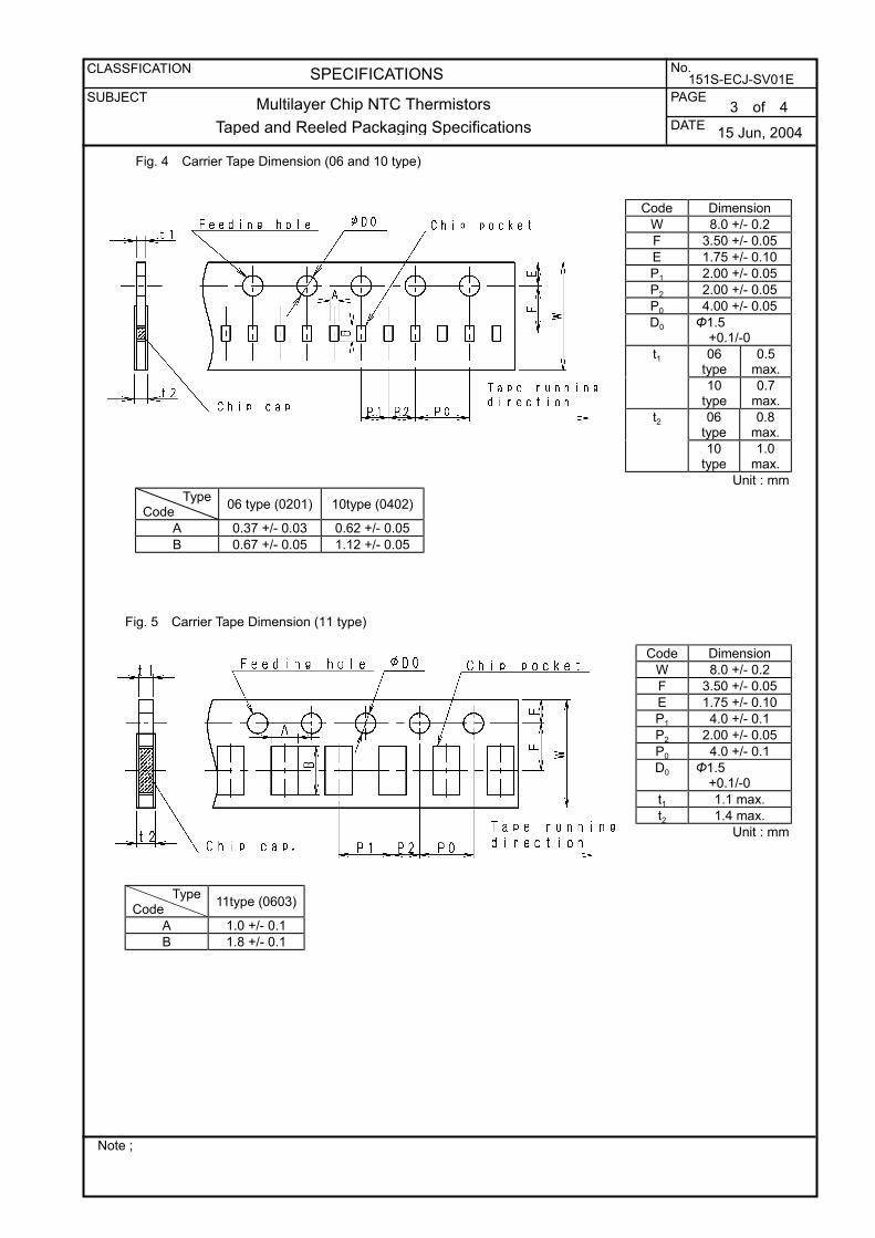
Fig. 4 Carrier Tape Dimension (06 and 10 type)
Code Dimension
W 8.0 +/- 0.2F 3.50 +/- 0.05E 1.75 +/- 0.10P1 2.00 +/- 0.05P2 2.00 +/- 0.05P0 4.00 +/- 0.05D0 Φ1.5
+0.1/-006
type0.5
max.t1
10type
0.7max.
06type
0.8max.
t2
10type
1.0max.
Unit : mm Type
Code 06 type (0201) 10type (0402)
A 0.37 +/- 0.03 0.62 +/- 0.05B 0.67 +/- 0.05 1.12 +/- 0.05
Fig. 5 Carrier Tape Dimension (11 type)
Code DimensionW 8.0 +/- 0.2F 3.50 +/- 0.05E 1.75 +/- 0.10P1 4.0 +/- 0.1P2 2.00 +/- 0.05P0 4.0 +/- 0.1D0 Φ1.5
+0.1/-0t1 1.1 max.t2 1.4 max.
Unit : mm
TypeCode 11type (0603)
A 1.0 +/- 0.1B 1.8 +/- 0.1
4 of 4
15 Jun, 2004
CLASSFICATION SPECIFICATIONS No.
SUBJECT PAGE
DATE
151S-ECJ-SV01E
Multilayer Chip NTC ThermistorsTaped and Reeled Packaging Specifications
Note ;
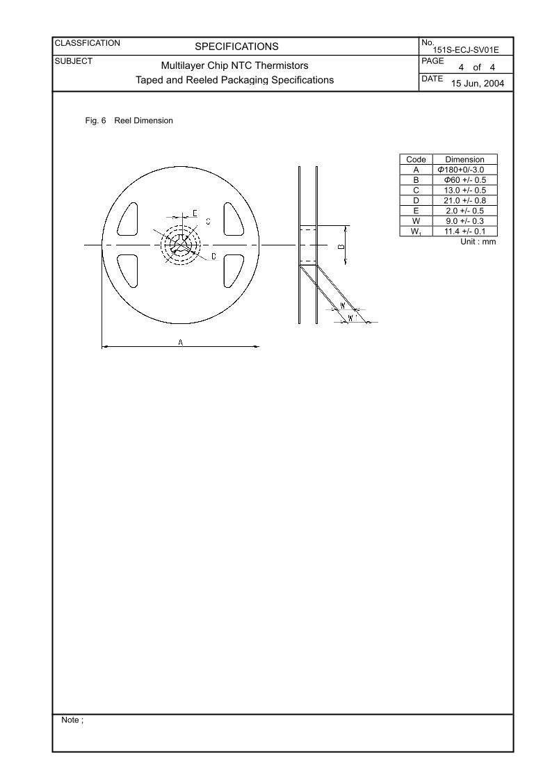
Fig. 6 Reel Dimension
Code Dimension
A Φ180+0/-3.0B Φ60 +/- 0.5C 13.0 +/- 0.5D 21.0 +/- 0.8E 2.0 +/- 0.5W 9.0 +/- 0.3W1 11.4 +/- 0.1
Unit : mm