2. introduction to diodes - university of california, san...
TRANSCRIPT
2. Introduction to Diodes
ECE 65, Winter 2013, F. Najmabadi
Lecture notes: page 2-1 to 2-19
Sedra & Smith (6th Ed): Sec. 3.* and 4.1-4.4 Sedra & Smith (5th Ed): Sec. 3.7* and Sec. 3.1-3.4
* Includes details of pn junction operation which is not covered in this course

Energy levels in an atom
F. Najmabadi, ECE 65, Winter2013, Intro to Diodes (2/29)
Electrons in the last filled energy level are called “valance” electrons and are responsible for the chemical properties of the material.
Discrete energy levels!
Each energy level can be filled with a finite number of electrons.
Lowest energy levels are filled first.
The larger the energy level, the larger is the spatial extent of electron orbital.
Nucleus position
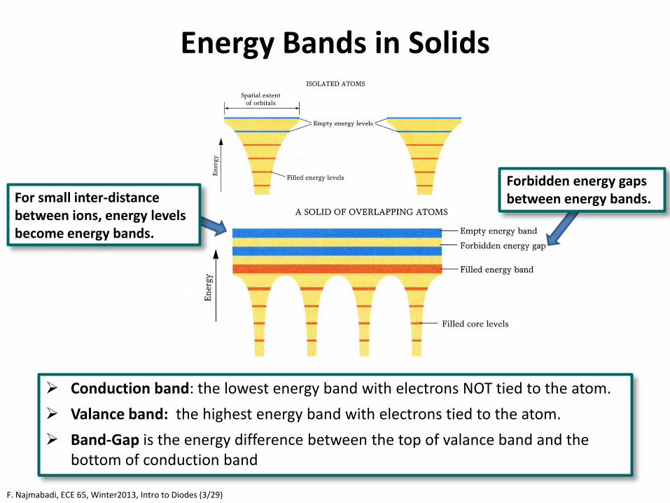
Energy Bands in Solids
F. Najmabadi, ECE 65, Winter2013, Intro to Diodes (3/29)
Conduction band: the lowest energy band with electrons NOT tied to the atom.
Valance band: the highest energy band with electrons tied to the atom.
Band-Gap is the energy difference between the top of valance band and the bottom of conduction band
For small inter-distance between ions, energy levels become energy bands.
Forbidden energy gaps between energy bands.

Differences among conductors, semiconductors and insulators
F. Najmabadi, ECE 65, Winter2013, Intro to Diodes (4/29)
In a metal, the conduction band is partially filled. These electron can move easily in the material and conduct heat and electricity (Conductors).
In a semi-conductor at 0 k the conduction band is empty and valance band is full. o The band-gap is small enough that at room temperature some electrons
move to the conduction band and material conduct electricity.
An insulator is similar to a semiconductor but with a larger band-gap. Thus, at room temperature very few electrons are in the conduction band.
Metal Semiconductor at T = 0 k
Semiconductor at T > 0 k
Insulator

Electric current in a semiconductor is due to the motion of electrons and “holes”
F. Najmabadi, ECE 65, Winter2013, Intro to Diodes (5/29)
At T > 0 k, some electrons are promoted to the conduction bands.
A current flows when electrons in the conduction band move across the material (e.g., due to an applied electric field).
A current also flows when electrons in the valance band jump between available slots in the valance bands (or “holes”). o An electron moving to the left = a hole
moving to the right!
o We call this is a “hole” current to differentiate this current due to conduction band electrons.
Conduction band
Valance band
“holes” or available slots in the valance band
Pure Si Crystal

Doping increases the number of charge carriers
F. Najmabadi, ECE 65, Winter2013, Intro to Diodes (6/29)
Doped n-type Semiconductor
Donor atom (P doping) has an extra electron which is in the conduction band.
Charge Carriers: o Electrons due to donor atoms o Electron-hole pairs due to thermal
excitation o e: majority carrier, h: minority carrier
Doped p-type Semiconductor
Acceptor atom (B doping) has one less electrons: a hole in the valance band.
Charge Carriers: o Holes due to acceptor atoms o Electron-hole pairs due to thermal
excitation o h: majority carrier, e: minority carrier
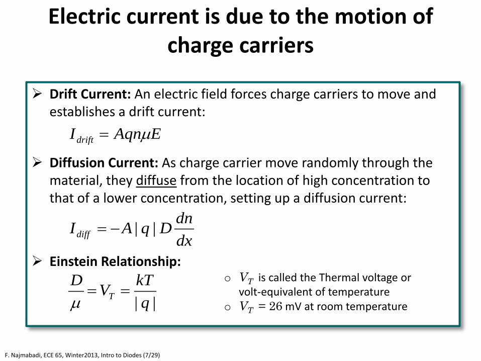
Electric current is due to the motion of charge carriers
F. Najmabadi, ECE 65, Winter2013, Intro to Diodes (7/29)
Drift Current: An electric field forces charge carriers to move and establishes a drift current:
Diffusion Current: As charge carrier move randomly through the material, they diffuse from the location of high concentration to that of a lower concentration, setting up a diffusion current:
Einstein Relationship: o VT is called the Thermal voltage or
volt-equivalent of temperature o VT = 26 mV at room temperature
EAqnIdrift µ=
||dxdnDqAIdiff −=
||
qkTVD
T ==µ

Junction diode
Simplified physical structure Construction on a CMOS chip

A pn junction with open terminals (excluding minority carriers)
F. Najmabadi, ECE 65, Winter2013, Intro to Diodes (9/29)
High concentration of h on the p side Holes diffuse towards the junction
High concentration of e on the n side Electrons diffuse towards the junction
n side is positively charged because it has lost electrons.
p side is negatively charged because it has lost holes.
A potential is formed which inhibits further diffusion of electron and holes (called junction built-in voltage)
Holes from the p side and electrons from the n side combine at the junction, forming a depletion region
Idif Idif

A pn junction with open terminals (including minority carriers)
F. Najmabadi, ECE 65, Winter2013, Intro to Diodes (10/29)
Thermally-generated minority carriers on the n side (holes) move toward the depletion region, and are swept into the p side by the potential where the combine with electrons. (similar process for minority carriers on the p side). This sets up a drift current, IS.
To preserve charge neutrality, a non-zero Idiff = IS should flow (height of potential is slightly lower).
Idiff scales exponentially with changes in the voltage barrier.
IS is independent of the voltage barrier but is a sensitive function of temperature.
Idif
IS

pn Junction with an applied voltage
F. Najmabadi, ECE 65, Winter2013, Intro to Diodes (11/29)
Reverse-Bias:
Height of the barrier is increased, reducing Idiff
Idiff approaches zero rapidly, with iD ≈ IS
A very small negative iD !
Forward-Bias:
Height of the barrier is decreased, increasing Idiff
Idiff increases rapidly with vD leading to iD ≈ Idiff
A very large positive iD !

Diode iv characteristics equation
F. Najmabadi, ECE 65, Winter2013, Intro to Diodes (12/29)
IS : Reverse Saturation Current (10-9 to 10-18 A)
VT : Volt-equivalent temperature (= 26 mV at room temperature)
n: Emission coefficient (1 ≤ n ≤ 2 for Si ICs)
( )1 / −= TD nVvSD eIi
:bias Reverse :bias Forward
3 ||For /
SD
nVvSD
TD
IieIi
nVvTD
−≈≈
≥
For derivation of diode iv equation, see Sedra & Smith Sec. 3
Sensitive to temperature:
IS doubles for every 7oC increase
VT = T(k) /11,600

Diode Limitations
F. Najmabadi, ECE 65, Winter2013, Intro to Diodes (13/29)
Thermal load, P = iD vD (typically specified as maximum iD )
Reverse Breakdown at Zener voltage (VZ) (due to Zener or avalanche effects)
Zener diodes are made specially to operate in this region safely!

How to solve diode circuits?

Diode circuit equations are nonlinear
F. Najmabadi, ECE 65, Winter2013, Intro to Diodes (15/29)
Two equations in two-unknowns to solve for iD and vD
Non-linear equation: cannot be solved analytically
Solution methods:
o Numerical (PSpice)
o Graphical (load-line)
o Approximation to get linear equations (diode piece-linear model)
( )1 :Eq.
:KVLelements allin current :KCL
/ −=
+=TD nVv
SD
DDi
D
eIiiv
vRivi

Graphical Solution (Load Line)
F. Najmabadi, ECE 65, Winter2013, Intro to Diodes (16/29)
( )1 :Eq.
:KVLelements allin current :KCL
/ −=
+=TD nVv
SD
DDi
D
eIiiv
vRivi
DDi vRiv +=
( )1 / −= TD nVvSD eIi
Intersection of two curves satisfies both equations and is the solution
vi
vi/R
vDQ
iDQ
Load Line

Diode piecewise-linear model: Diode iv is approximated by two lines
F. Najmabadi, ECE 65, Winter2013, Intro to Diodes (17/29)
Constant Voltage Model
Sifor V 7.06.0 voltage,in"-cut" and 0 :OFF Diode
0 and :ON Diode
0
0
0
−=<=≥=
D
DDD
DDD
VVvi
iVv
Circuit Models: ON: OFF:
Diode ON
Diode OFF
VD0

Recipe for solving diode circuits (State of diode is unknown before solving the circuit)
F. Najmabadi, ECE 65, Winter2013, Intro to Diodes (18/29)
1. Write down all circuit equations and simplify as much as possible
2. Assume diode is one state (either ON or OFF). Use the diode equation for that state to solve the circuit equations and find iD and vD
3. Check the inequality associated with that state (“range of validity”). If iD or vD satisfy the inequality, assumption is correct. If not, go to step 2 and start with the other state.
NOTE: o This method works only if we know the values of all elements so
that we can find numerical values of iD and vD .
o For complicated circuits use diode circuit models.

F. Najmabadi, ECE 65, Winter2013, Intro to Diodes (19/29)
Example 1: Find iD and vD for R = 1k, vi = 5 V, and Si Diode (VD0 = 0.7 V).
DD
DDi
D
vivRiv
i
+=
+=
10 5
:KVLelements allin current :KCL
3
incorrect Assumption V 7.0V 5V 5 0 10 5
and 0 :OFF is diode Assume
0
30
→=>==→+×=
<=
DD
DD
DDD
Vvvv
Vvi
correct Assumption 0mA 3.4mA 3.4 7.0 10 5
0 and V 7.0 :ON is diode Assume3
0
→>==→+=
≥==
D
DD
DDD
iii
iVv
Diode is ON with iD = 4.3 mA and vD = 0.7 V).

F. Najmabadi, ECE 65, Winter2013, Intro to Diodes (20/29)
Example 1: Find iD and vD for R = 1k, vi = 5 V, and Si Diode (VD0 = 0.7 V).
Incorrect! V 7.0V 5V 5 0 10 5
0
3
→=>==→+×=
DD
DD
Vvvv
Correct! 0mA 3.4mA 3.4 7.0 10 5 3
→≥==→+=
D
DD
iii
Diode is ON with iD = 4.3 mA and , vD = 0.7 V.
Solution with diode circuit models:
0 and 0 :OFF Diode DDD Vvi <= 0 and :ON Diode 0 ≥= DDD iVv
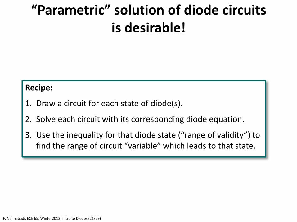
“Parametric” solution of diode circuits is desirable!
F. Najmabadi, ECE 65, Winter2013, Intro to Diodes (21/29)
Recipe:
1. Draw a circuit for each state of diode(s).
2. Solve each circuit with its corresponding diode equation.
3. Use the inequality for that diode state (“range of validity”) to find the range of circuit “variable” which leads to that state.

F. Najmabadi, ECE 65, Winter2013, Intro to Diodes (22/29)
Example 2: Find vD in the circuit below for all vi .
00 0R
DiDD
iDDi
VvVvvvvv
<→<=→+×=
0
00
0
0/)( R
DiD
DiDDDi
DD
VviRVviViv
Vv
≥→≥−=→+=
=
0 and 0 :OFF Diode DDD Vvi <= 0 and :ON Diode 0 ≥= DDD iVv
iDDi
DDDi
vvVvVvVv
=<=≥
and OFF Diode ,For and ON Diode ,For
0
00
Solution
Inequality

Accuracy of Constant-Voltage Model
F. Najmabadi, ECE 65, Winter2013, Intro to Diodes (23/29)
Constant Voltage Model Diode ON
Diode OFF
VD0
Diode can be in forward bias with vD as small as 0.4 V when iD is small (Lab 4)
In forward bias, “cut-in” voltage (VD0) can vary between 0.6 & 0.8 V (± 0.1 V)
In forward bias, diode voltage changes slightly as current changes (discussed later in small signal model)

Other types of diodes
F. Najmabadi, ECE 65, Winter2013, Intro to Diodes (24/29)
Schottky Barrier Diode
Large IS and VD0 ≈ 0.3 V
Zener Diode
Made specially to operate in the
reverse breakdown region. Useful as a “reference” voltage in
many circuits.
Light-emitting diode (LED)
VD0 = 1.7 – 1.9 V

Zener Diode piecewise-linear model
F. Najmabadi, ECE 65, Winter2013, Intro to Diodes (25/29)
0 and : Zener and 0 :OFF Diode
0 and :ON Diode
0
0
≤−=<<−=
≥=
DZD
DDZD
DDD
iVvVvVi
iVv
Diode ON
Diode OFF
VD0
Zener
Circuit Models: ON: OFF: Zener:

Zener diodes are useful in providing reference voltages
F. Najmabadi, ECE 65, Winter2013, Intro to Diodes (26/29)
Example 3: Find the iv characteristics of the two-terminal circuit below (for vo > 0)
0 and :regionin Zener diode Assume 1)
≤−= DZD iVv
constant :KVL ==−= ZDo Vvv
RVvii
VRiviii
ZsoD
Zs
oD
−−=
+=−=
:KVL :KCL
(Independent of io !)
0for region in Zener Diode ≤Di
max, 0 oZs
oD iR
Vvii =−
≤→≤
Acts as independent voltage sources even if vs changes!
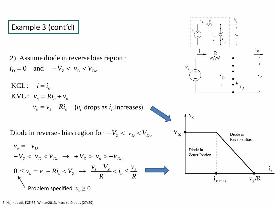
F. Najmabadi, ECE 65, Winter2013, Intro to Diodes (27/29)
Example 3 (cont’d)
DoDZD VvVi <<−= and 0:region bias reversein diode Assume 2)
oso
oos
o
RivvvRiv
ii
−=+=
=
:KVL :KCL
(vo drops as io increases)
DoDZ VvV <<− for region bias-reversein Diode
Rvi
RVvVRivv
VvVVvVvv
so
ZsZoso
DooZDoDZ
Do
≤<−
→<−=≤
−>>+→<<−−=
0
Problem specified vo ≥ 0
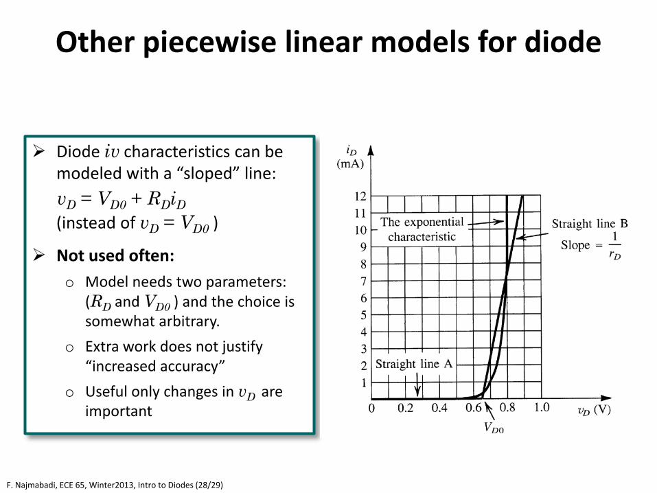
Other piecewise linear models for diode
F. Najmabadi, ECE 65, Winter2013, Intro to Diodes (28/29)
Diode iv characteristics can be modeled with a “sloped” line:
vD = VD0 + RDiD (instead of vD = VD0 )
Not used often: o Model needs two parameters:
(RD and VD0 ) and the choice is somewhat arbitrary.
o Extra work does not justify “increased accuracy”
o Useful only changes in vD are important

Other piecewise linear models for diode
F. Najmabadi, ECE 65, Winter2013, Intro to Diodes (29/29)
Diode Zener region can also be modeled with a “sloped” line:
vD = −VZ0 + RZ iD (instead of vD = −VZ0 )
Useful when changes in vD is important. o For example, If we use this
model for Example 2, we find*:
constant of instead
0
==
−≈
Zo
oZZo
Vv
iRVv
* See lecture notes, page 2-18