2009 vcsel-based miniature laser-self-mixing interferometer with
TRANSCRIPT
laser self-mixingusing Doppler effect
reflectingobject
VCSEL-based miniature laser-self-mixing interferometer with integrated optical and electronic components
Armand Pruijmboom a, Silvia Booij a, Marcel Schemmann a, Klaus Werner a, Pieter Hoeven a,
Henri van Limpt a, Steffan Intemann b, Rafael Jordan c, Thomas Fritzsch c, Hermann Oppermann c, Michel Barge d,
a Philips Laser Sensors, Hurksestraat 2C, 5652AJ Eindhoven, The Netherlands b Philips Technologie GmbH, U-L-M Photonics, Lise-Meitnerstrasse 13, 89081 Ulm, Germany
c Fraunhofer IZM, Gustav-Meyer-Allee 25, 13355 Berlin, Germany d Heptagon Oy, Moosstrasse 2, 8803 Rueschlikon, Switzerland
ABSTRACT
It has been previously published [1] how, using two separate Vertical-Cavity-Surface-Emitting-Lasers (VCSELs), a miniature laser-Doppler interferometer can be made for quasi-three-dimensional displacement measurements. For the use in consumer applications as PC-mice, the manufacturing costs of such sensors need to be minimized. This paper describes the fabrication of a low-cost laser-self-mixing sensor by integrating silicon and GaAs components using flip-chip technology. Wafer-scale lens replication on GaAs wafers is used to achieve integrated optics. In this way a sensor was realized without an external lens and that uses only a single GaAs VCSEL crystal, while maintaining its quasi-three-dimensional sensor capabilities.
Keywords: Laser-self-mixing interferometers, PC-mice, GaAs VCSEL, Hybrid integration of silicon and GaAs, Wafer-scale micro-lens replication, Flip-chip connection, Solder bumps
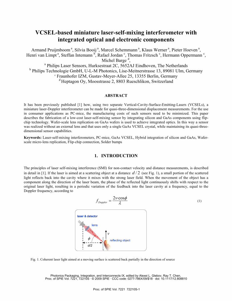
1. INTRODUCTION The principles of laser self-mixing interference (SMI) for non-contact velocity and distance measurements, is described in detail in [1]. If the laser is aimed at a scattering object at a distance 2/d (see Fig. 1), a small portion of the scattered light reflects back into the cavity where it mixes with the strong laser field. When the movement of the object has a component along the direction of the laser beam, the phase of the reflected light continuously shifts with respect to the original laser light, resulting in a periodic variation of the feedback into the laser cavity at a frequency, equal to the Doppler frequency, according to
λφcos2 ⋅= vfDoppler (1)
Fig. 1. Coherent laser light aimed at a moving surface is scattered back partially in the direction of source
lens
laser & detector
reflecting objectφ
d/2
v
lens
laser & detector
reflecting objectφ
d/2
v
Photonics Packaging, Integration, and Interconnects IX, edited by Alexei L. Glebov, Ray T. Chen, Proc. of SPIE Vol. 7221, 72210S · © 2009 SPIE · CCC code: 0277-786X/09/$18 · doi: 10.1117/12.808810
Proc. of SPIE Vol. 7221 72210S-1
F
Here φcos⋅v is the velocity component along the direction of the laser beam in Fig. 1, and λ the wavelength of the laser. Thus the feedback from this moving object generates a changing interference signal inside the laser cavity with this Doppler frequency, and hence the laser output power is modulated with a frequency, from which the velocity of the scattering object can be derived, according to Equation (1).
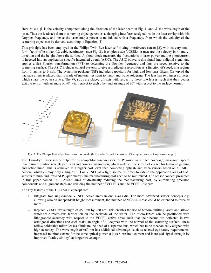
This principle has been employed in the Philips Twin-Eye laser self-mixing interference sensor [2], with its very small form factor of less than 0.2 cubic centimeters (see Fig. 2). It employs two VCSELs to measure the velocity in x- and y-direction and the height above the surface. A photo diode measures the fluctuations in laser power and the photocurrent is injected into an application-specific integrated circuit (ASIC). The ASIC converts this signal into a digital signal and applies a fast Fourier transformation (FFT) to determine the Doppler frequency and thus the speed relative to the scattering surface. The ASIC includes control systems to give a predictable resolution as a function of speed, in a regime from 0.1mm/s to 6 m/s. The system-in-package (SiP) includes capacitors for high and low-pass filters. On top of the package a lens is placed that is made of material resistant to hand- and wave soldering. The lens has two inner surfaces, which share the outer surface. The VCSELs are placed off-axis with respect to these two lenses, such that their beams exit the sensor with an angle of 90° with respect to each other and an angle of 30° with respect to the surface normal.
Fig. 2. The Philips Twin-Eye laser sensor on scale (left) and enlarged the inside of the system-in-package sensor (right)
The Twin-Eye Laser sensor outperforms competitor laser-sensors for PC-mice in surface coverage, maximum speed, maximum resolution (counts per inch) and power consumption, which makes it the sensor of choice for high-end gaming and office mice. This is achieved at a higher cost level than competing optical- and laser-sensors based on a CMOS camera, which employ only a single LED or VCSEL as a light source. In order to extend the application area of SMI sensors to mid- and low-end PC-peripherals, the manufacturing cost need to be minimized. The sensor concept presented in this paper named “TELEMUS” aims at drastically reducing the manufacturing cost, by eliminating precision components and alignment steps and reducing the number of VCSELs and the VCSEL-die area.
The key features of the TELEMUS concept are:
1. Integrate two single-mode VCSEL active areas in one GaAs die. For more advanced sensor concepts e.g. allowing also an independent height measurement, the number of VCSEL mesas could be extended to three or more.
2. Replace VCSEL wavelength of 850 nm by 960 nm. This enables the use of bottom emitting lasers and allows wafer-scale micro-lens fabrication on the backside of the wafer. The micro-lenses can be positioned with lithographic accuracy with respect to the VCSEL active areas such that their beams are deflected in two orthogonal directions and each make an angle of 30 degrees with the normal of the scattering surface. These reflow solderable micro-lenses eliminate the need of a separate lens, which has to be mechanically aligned with high accuracy. The wavelength of 960 nm has additional advantages such as relaxed eye-safety requirements, increased monitor current for the same optical power, a lower threshold current and increased signal strength by improved “dark visibility” at longer wavelength.
Proc. of SPIE Vol. 7221 72210S-2
3. Eliminate wire bonding on GaAs die, and replace by electrical contacting through solder-bumps and flip-chip assembly on a silicon photo-diode (PD). This minimizes the size of bonding pads and hence of GaAs die area. The VCSEL active areas also emit light from the wafer front side. This light illuminates the photosensitive area of the PD. The electrical connections to the VCSEL are made using isolated tracks on the PD. Pads large enough for wire bonding are made on this photo-diode, which has a comparatively low cost per area.
4. The functionality of the optical engine, i.e. the VCSEL with integrated micro-lens flip-chip assembled on the silicon PD, can be tested by probe testing on the PD wafer. This is done before the PD wafer is diced to separate the individual optical engines. This enables assembling only known good optical engines, reducing yield losses at final testing after sensor assembly.
5. Replace the lead-frame with molded cavity of the Twin-Eye Laser sensor by a printed circuit board (PCB). Because the need for a separate lens has been eliminated, all mechanical tolerances can be significantly relaxed. Additionally this removes any temperature constraints for assembling the sensor in the PCB of the application. Therefore, surface mounted device (SMD) assembly by reflow soldering can be used.
2. WAFER-SCALE MICRO-LENS FABRICATION In this section we elaborate on the wafer-scale micro-lens. For the sensor to work properly, the amount of light that is scattered back from the surface and that propagates back to the VCSEL cavity and the detector should be maximized. Therefore a lens is needed, but it should be as low-cost as possible. Wafer-scale optics can keep the cost of the lenses as low as possible since the lenses are fabricated on the VCSEL-wafer before sawing. This way the time-consuming and therefore costly alignment of the lens on the VCSEL only needs to be done once for the entire wafer.
This section describes the requirements to the lenses, the design method and the resulting lens specification, the lens fabrication technology and the actually realized lens.
2.1 Lens Requirements
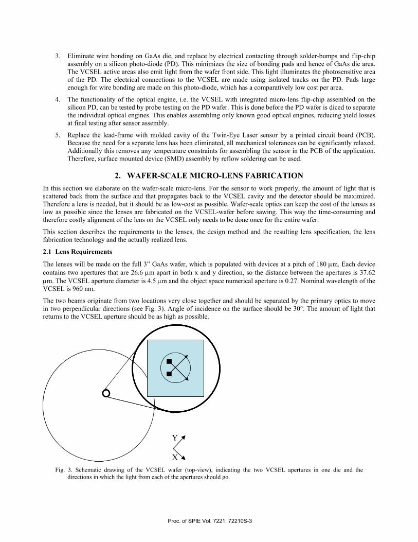
The lenses will be made on the full 3” GaAs wafer, which is populated with devices at a pitch of 180 μm. Each device contains two apertures that are 26.6 μm apart in both x and y direction, so the distance between the apertures is 37.62 μm. The VCSEL aperture diameter is 4.5 μm and the object space numerical aperture is 0.27. Nominal wavelength of the VCSEL is 960 nm.
The two beams originate from two locations very close together and should be separated by the primary optics to move in two perpendicular directions (see Fig. 3). Angle of incidence on the surface should be 30°. The amount of light that returns to the VCSEL aperture should be as high as possible.
Fig. 3. Schematic drawing of the VCSEL wafer (top-view), indicating the two VCSEL apertures in one die and the
directions in which the light from each of the apertures should go.
X
Y
Proc. of SPIE Vol. 7221 72210S-3
El
El
El
El
L4
2.2 Design method and resulting lens specification
Due to symmetry of the system one light path from one VCSEL is simulated only. The lens has a fixed decentering with respect to the VCSEL aperture of 26.6 micrometer. The lens is designed with Zemax ray-tracing software, to be an asphere with variable radius and conic constant. The merit function is determined by the angle of incidence on the object surface and the spot size of the beam on the surface. Table 1 shows the results of the optimized design.
Total height of lens (incl. homogeneous layer) 50 μm (-1 +3.5 μm) Maximum height of homogeneous layer 20 μm Aspheric lens shape accuracy +/- 200 nm rms Diameter 90 μm Radius 33.23 μm Conic constant -0.908 Maximum lens sag 32 μm
Table1. Optimum lens-shape design as determined by Zemax ray-tracing software optimization (according to [ISO 10110])
2.3 Lens fabrication
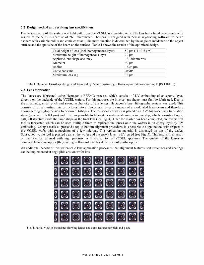
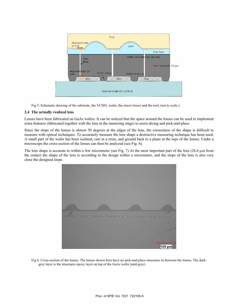
The lenses are fabricated using Heptagon’s REEMO process, which consists of UV embossing of an epoxy layer, directly on the backside of the VCSEL wafers. For this purpose, the inverse lens shape must first be fabricated. Due to the small size, small pitch and strong asphericity of the lenses, Heptagon’s laser lithography system was used. This consists of direct writing microstructures into a photo-resist layer by means of a modulated laser-beam and therefore allows getting high-precision free-form 3D-shapes. The resist-coated wafer is placed on a X-Y high-accuracy translation stage (precision +/- 0.4 μm) and it is thus possible to fabricate a wafer-scale master in one step, which consists of up to 140,000 structures with the same shape as the final lens (see Fig. 4). Once the master has been completed, an inverse soft tool is fabricated which can be used multiple times to replicate the lenses onto the wafers in an epoxy layer by UV embossing. Using a mask-aligner and a top-to-bottom alignment procedure, it is possible to align the tool with respect to the VCSEL-wafer with a precision of a few microns. The replication material is dispensed on top of the wafer. Subsequently, the tool is pressed against the wafer and the epoxy layer is UV cured (see Fig. 5). This results in an array of micro-lenses, aligned with high precision with respect to the VCSEL apertures. The quality of the lenses is comparable to glass optics (they are e.g. reflow solderable) at the price of plastic optics.
An additional benefit of this wafer-scale lens application process is that alignment features, test structures and coatings can be implemented at negligible cost on wafer level.
Fig. 4. Partial view of the master showing lenses and extra features for pick-and-place
Proc. of SPIE Vol. 7221 72210S-4
Alignment markon tool
Tool
Sawjanes
Alignment mark onwafer VOSEL mesa
Lens
AL rJ A
Glass substrate 500 jm thick
Base layer
Wafer back sid6 (back lapped)
Wafer mesa s
jaA substrat 100 pm
100 pm
Fig 5. Schematic drawing of the substrate, the VCSEL wafer, the micro lenses and the tool, (not to scale.)
2.4 The actually realized lens
Lenses have been fabricated on GaAs wafers. It can be noticed that the space around the lenses can be used to implement extra-features (fabricated together with the lens at the mastering stage) to assist dicing and pick-and-place.
Since the slope of the lenses is almost 50 degrees at the edges of the lens, the correctness of the shape is difficult to measure with optical techniques. To accurately measure the lens shape a destructive measuring technique has been used. A small part of the wafer has been isolated, cast in a resin, and ground back to a plane at the tops of the lenses. Under a microscope the cross-section of the lenses can then be analyzed (see Fig. 6).
The lens shape is accurate to within a few micrometer (see Fig. 7) At the most important part of the lens (26.6 μm from the center) the shape of the lens is according to the design within a micrometer, and the slope of the lens is also very close the designed slope.
Fig 6. Cross-section of the lenses. The lenses shown here have no pick-and-place structures in between the lenses. The dark-grey layer is the structures epoxy layer on top of the GaAs wafer (mid-grey)
Proc. of SPIE Vol. 7221 72210S-5
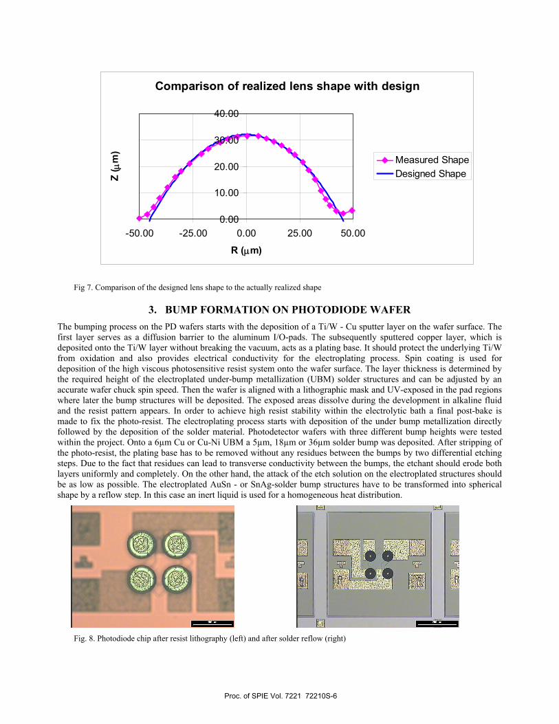
Fig 7. Comparison of the designed lens shape to the actually realized shape
3. BUMP FORMATION ON PHOTODIODE WAFER The bumping process on the PD wafers starts with the deposition of a Ti/W - Cu sputter layer on the wafer surface. The first layer serves as a diffusion barrier to the aluminum I/O-pads. The subsequently sputtered copper layer, which is deposited onto the Ti/W layer without breaking the vacuum, acts as a plating base. It should protect the underlying Ti/W from oxidation and also provides electrical conductivity for the electroplating process. Spin coating is used for deposition of the high viscous photosensitive resist system onto the wafer surface. The layer thickness is determined by the required height of the electroplated under-bump metallization (UBM) solder structures and can be adjusted by an accurate wafer chuck spin speed. Then the wafer is aligned with a lithographic mask and UV-exposed in the pad regions where later the bump structures will be deposited. The exposed areas dissolve during the development in alkaline fluid and the resist pattern appears. In order to achieve high resist stability within the electrolytic bath a final post-bake is made to fix the photo-resist. The electroplating process starts with deposition of the under bump metallization directly followed by the deposition of the solder material. Photodetector wafers with three different bump heights were tested within the project. Onto a 6µm Cu or Cu-Ni UBM a 5µm, 18µm or 36µm solder bump was deposited. After stripping of the photo-resist, the plating base has to be removed without any residues between the bumps by two differential etching steps. Due to the fact that residues can lead to transverse conductivity between the bumps, the etchant should erode both layers uniformly and completely. On the other hand, the attack of the etch solution on the electroplated structures should be as low as possible. The electroplated AuSn - or SnAg-solder bump structures have to be transformed into spherical shape by a reflow step. In this case an inert liquid is used for a homogeneous heat distribution.
Fig. 8. Photodiode chip after resist lithography (left) and after solder reflow (right)
Comparison of realized lens shape with design
0.00
10.00
20.00
30.00
40.00
-50.00 -25.00 0.00 25.00 50.00
R (μm)
Z ( μ
m)
Measured ShapeDesigned Shape
Proc. of SPIE Vol. 7221 72210S-6
4..
4. ASSEMBLY OF VCSELS ON PHOTODIODES
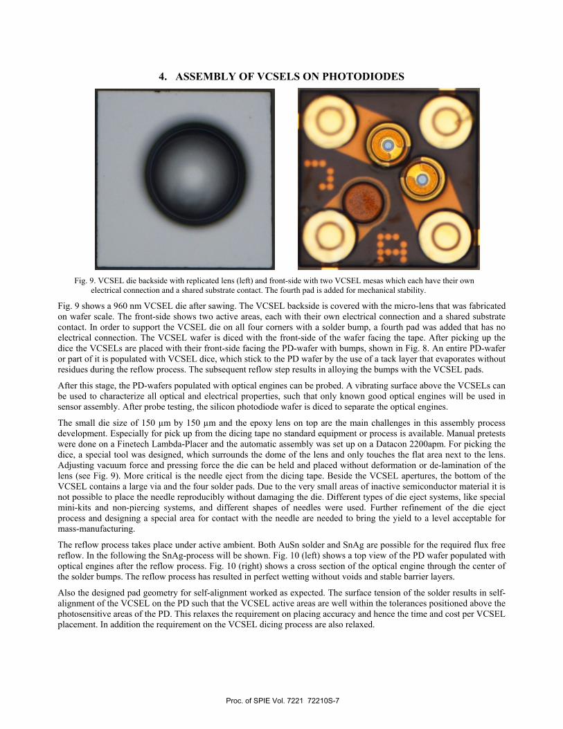
Fig. 9. VCSEL die backside with replicated lens (left) and front-side with two VCSEL mesas which each have their own
electrical connection and a shared substrate contact. The fourth pad is added for mechanical stability.
Fig. 9 shows a 960 nm VCSEL die after sawing. The VCSEL backside is covered with the micro-lens that was fabricated on wafer scale. The front-side shows two active areas, each with their own electrical connection and a shared substrate contact. In order to support the VCSEL die on all four corners with a solder bump, a fourth pad was added that has no electrical connection. The VCSEL wafer is diced with the front-side of the wafer facing the tape. After picking up the dice the VCSELs are placed with their front-side facing the PD-wafer with bumps, shown in Fig. 8. An entire PD-wafer or part of it is populated with VCSEL dice, which stick to the PD wafer by the use of a tack layer that evaporates without residues during the reflow process. The subsequent reflow step results in alloying the bumps with the VCSEL pads.
After this stage, the PD-wafers populated with optical engines can be probed. A vibrating surface above the VCSELs can be used to characterize all optical and electrical properties, such that only known good optical engines will be used in sensor assembly. After probe testing, the silicon photodiode wafer is diced to separate the optical engines.
The small die size of 150 µm by 150 µm and the epoxy lens on top are the main challenges in this assembly process development. Especially for pick up from the dicing tape no standard equipment or process is available. Manual pretests were done on a Finetech Lambda-Placer and the automatic assembly was set up on a Datacon 2200apm. For picking the dice, a special tool was designed, which surrounds the dome of the lens and only touches the flat area next to the lens. Adjusting vacuum force and pressing force the die can be held and placed without deformation or de-lamination of the lens (see Fig. 9). More critical is the needle eject from the dicing tape. Beside the VCSEL apertures, the bottom of the VCSEL contains a large via and the four solder pads. Due to the very small areas of inactive semiconductor material it is not possible to place the needle reproducibly without damaging the die. Different types of die eject systems, like special mini-kits and non-piercing systems, and different shapes of needles were used. Further refinement of the die eject process and designing a special area for contact with the needle are needed to bring the yield to a level acceptable for mass-manufacturing.
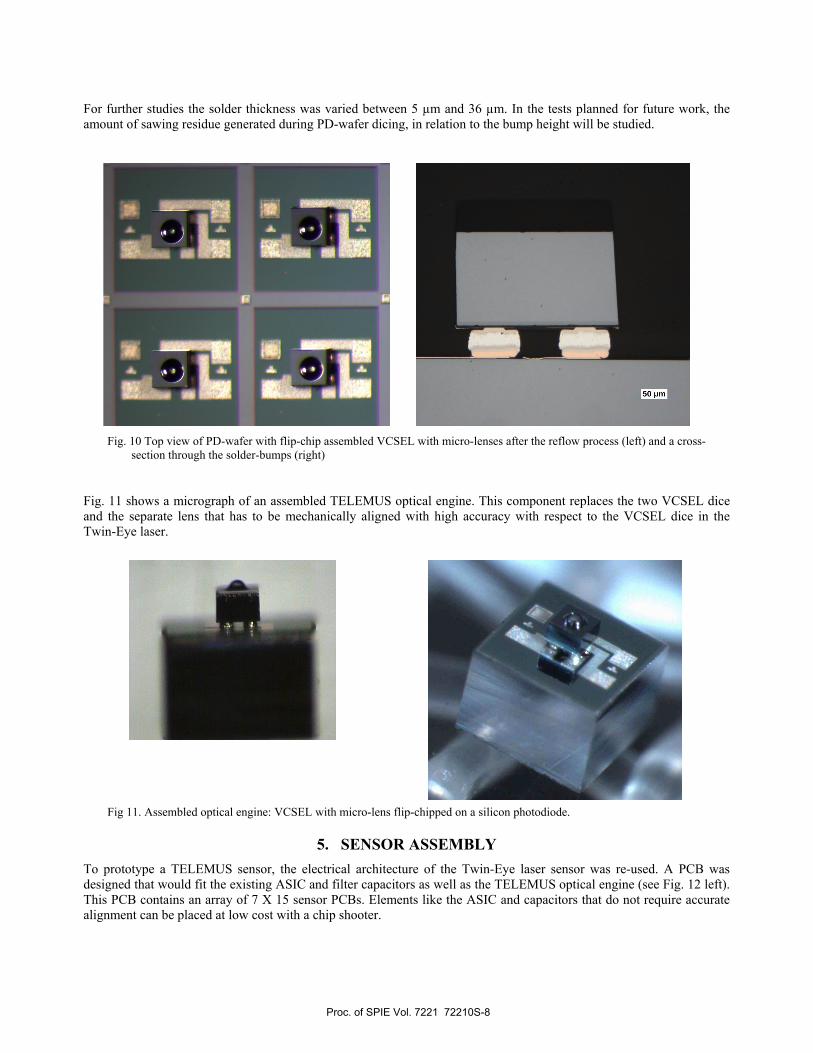
The reflow process takes place under active ambient. Both AuSn solder and SnAg are possible for the required flux free reflow. In the following the SnAg-process will be shown. Fig. 10 (left) shows a top view of the PD wafer populated with optical engines after the reflow process. Fig. 10 (right) shows a cross section of the optical engine through the center of the solder bumps. The reflow process has resulted in perfect wetting without voids and stable barrier layers.
Also the designed pad geometry for self-alignment worked as expected. The surface tension of the solder results in self-alignment of the VCSEL on the PD such that the VCSEL active areas are well within the tolerances positioned above the photosensitive areas of the PD. This relaxes the requirement on placing accuracy and hence the time and cost per VCSEL placement. In addition the requirement on the VCSEL dicing process are also relaxed.
Proc. of SPIE Vol. 7221 72210S-7
50 pm
For further studies the solder thickness was varied between 5 µm and 36 µm. In the tests planned for future work, the amount of sawing residue generated during PD-wafer dicing, in relation to the bump height will be studied.
Fig. 10 Top view of PD-wafer with flip-chip assembled VCSEL with micro-lenses after the reflow process (left) and a cross-
section through the solder-bumps (right)
Fig. 11 shows a micrograph of an assembled TELEMUS optical engine. This component replaces the two VCSEL dice and the separate lens that has to be mechanically aligned with high accuracy with respect to the VCSEL dice in the Twin-Eye laser.
Fig 11. Assembled optical engine: VCSEL with micro-lens flip-chipped on a silicon photodiode.
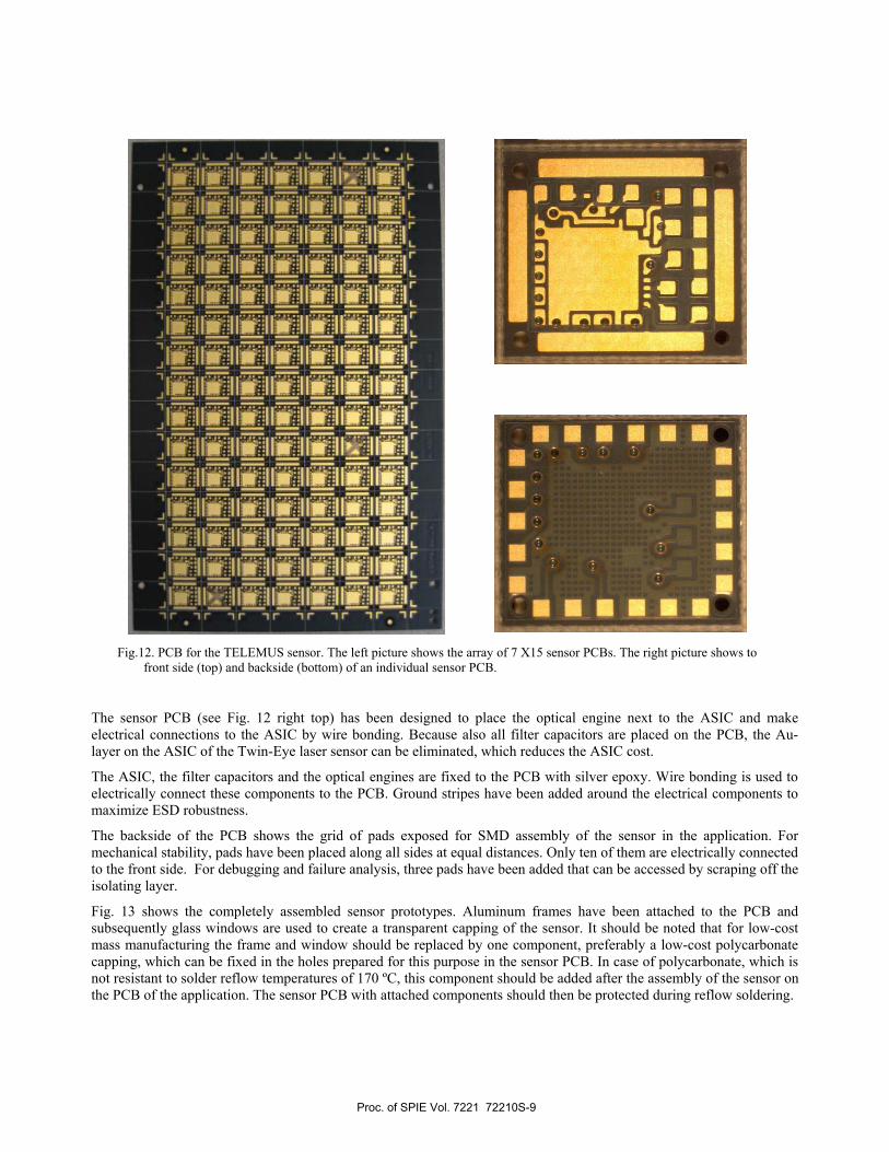
5. SENSOR ASSEMBLY To prototype a TELEMUS sensor, the electrical architecture of the Twin-Eye laser sensor was re-used. A PCB was designed that would fit the existing ASIC and filter capacitors as well as the TELEMUS optical engine (see Fig. 12 left). This PCB contains an array of 7 X 15 sensor PCBs. Elements like the ASIC and capacitors that do not require accurate alignment can be placed at low cost with a chip shooter.
Proc. of SPIE Vol. 7221 72210S-8
SS
.JL
JL iL
JL
JL .J
L.J
L JL
-JL
JL-.
JL J
L ..J
LJL
.JLJ
L
1 i1
!!III
i!iII
II II
IIIl I
II!III
111I
I!1
' IiII
i:ItiI
i!ii
k;iii
ii ii
i iiii
i I:1
liI_1
-LI
W 1
W-
S ;J1p
U....
:U
1kUU.
H
Fig.12. PCB for the TELEMUS sensor. The left picture shows the array of 7 X15 sensor PCBs. The right picture shows to front side (top) and backside (bottom) of an individual sensor PCB.
The sensor PCB (see Fig. 12 right top) has been designed to place the optical engine next to the ASIC and make electrical connections to the ASIC by wire bonding. Because also all filter capacitors are placed on the PCB, the Au-layer on the ASIC of the Twin-Eye laser sensor can be eliminated, which reduces the ASIC cost.
The ASIC, the filter capacitors and the optical engines are fixed to the PCB with silver epoxy. Wire bonding is used to electrically connect these components to the PCB. Ground stripes have been added around the electrical components to maximize ESD robustness.
The backside of the PCB shows the grid of pads exposed for SMD assembly of the sensor in the application. For mechanical stability, pads have been placed along all sides at equal distances. Only ten of them are electrically connected to the front side. For debugging and failure analysis, three pads have been added that can be accessed by scraping off the isolating layer.
Fig. 13 shows the completely assembled sensor prototypes. Aluminum frames have been attached to the PCB and subsequently glass windows are used to create a transparent capping of the sensor. It should be noted that for low-cost mass manufacturing the frame and window should be replaced by one component, preferably a low-cost polycarbonate capping, which can be fixed in the holes prepared for this purpose in the sensor PCB. In case of polycarbonate, which is not resistant to solder reflow temperatures of 170 ºC, this component should be added after the assembly of the sensor on the PCB of the application. The sensor PCB with attached components should then be protected during reflow soldering.
Proc. of SPIE Vol. 7221 72210S-9
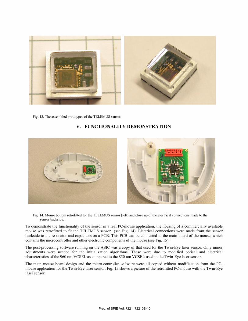
Fig. 13. The assembled prototypes of the TELEMUS sensor.
6. FUNCTIONALITY DEMONSTRATION
Fig. 14. Mouse bottom retrofitted for the TELEMUS sensor (left) and close up of the electrical connections made to the sensor backside.
To demonstrate the functionality of the sensor in a real PC-mouse application, the housing of a commercially available mouse was retrofitted to fit the TELEMUS sensor (see Fig. 14). Electrical connections were made from the sensor backside to the resonator and capacitors on a PCB. This PCB can be connected to the main board of the mouse, which contains the microcontroller and other electronic components of the mouse (see Fig. 15).
The post-processing software running on the ASIC was a copy of that used for the Twin-Eye laser sensor. Only minor adjustments were needed for the initialization algorithms. These were due to modified optical and electrical characteristics of the 960 nm VCSEL as compared to the 850 nm VCSEL used in the Twin-Eye laser sensor.
The main mouse board design and the micro-controller software were all copied without modification from the PC-mouse application for the Twin-Eye laser sensor. Fig. 15 shows a picture of the retrofitted PC-mouse with the Twin-Eye laser sensor.
Proc. of SPIE Vol. 7221 72210S-10
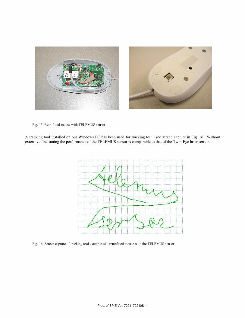
Fig. 15. Retrofitted mouse with TELEMUS sensor
A tracking tool installed on our Windows PC has been used for tracking test (see screen capture in Fig. 16). Without extensive fine-tuning the performance of the TELEMUS sensor is comparable to that of the Twin-Eye laser sensor.
Fig. 16. Screen capture of tracking tool example of a retrofitted mouse with the TELEMUS sensor
Proc. of SPIE Vol. 7221 72210S-11
7. CONCLUSIONS We have demonstrated that a quasi-3D displacement sensor based on self-mixing interference can be realized using a single GaAs VCSEL die. Optical elements for deflection and focusing were successfully integrated using wafer-scale micro-lens fabrication, thus eliminating the need for external optical elements. The optical engines for the sensor were realized by flip-chip assembly of the VCSELs with micro-lens, on low-cost silicon photodiodes. Low-cost packaging of the sensor was realized by placing the optical engines on a printed circuit board containing an ASIC and filter capacitors. A simple transparent window has been used to cap the sensor.
With the above result we have shown that self-mixing interference sensors, which have superior performance over camera-based optical and laser-sensor devices, can be made at the cost level required for mainstream consumer products. For industrialization of the assembly process, further improvements are needed, especially in the area of automated picking and placing of small GaAs dice.
8. ACKNOWLEDGEMENTS The authors would like to acknowledge Robin Huang, Jerry Chien and Perry Ho of Elite Advanced Laser Corporation, Taipei Hsien, Taiwan, R.O.C. for their contributions in prototyping the TELEMUS sensor.
This work is funded in part by the Dutch National Smartmix project Memphis
9. REFERENCES [1] VCSEL-based miniature laser-Doppler interferometer, Armand Pruijmboom, Marcel Schemmann, Jochen Hellmig,
Jeroen Schutte, Holger Moench, Joseph Pankert, Vertical-Cavity Surface-Emitting Lasers XII, Proceedings of the SPIE, Volume 6908, pp. 69080I-69080I-7 (2008).
[2] Philips Laser Sensors home page: http://www.philips.com/lasersensors
Proc. of SPIE Vol. 7221 72210S-12