2017 inemi roadmap highlights impacting board assembly...
TRANSCRIPT
2017 iNEMI Roadmap
Highlights Impacting
Board Assembly Over
the Next 5-10 Years
Speaker: Bill Bader, iNEMI
SMTAI 2017
September 18, 2017
Rosemont Convention Center
Rosemont, IL
Topics
iNEMI Introduction
iNEMI Roadmap Process Overview/Statistics
Situation Analysis
Technology Needs
Strategic Concerns
Paradigm Shifts
IoT/Wearables Product Emulator Highlights
Board Assembly Chapter Highlights
Optoelectronic Chapter Highlights
iNEMI Collaboration Projects
Summary/Next Steps
2
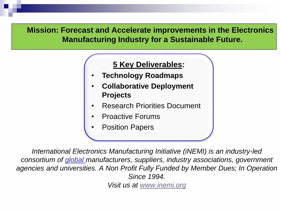
About iNEMI
International Electronics Manufacturing Initiative (iNEMI) is an industry-led
consortium of global manufacturers, suppliers, industry associations, government
agencies and universities. A Non Profit Fully Funded by Member Dues; In Operation
Since 1994.
Visit us at www.inemi.org
5 Key Deliverables:
• Technology Roadmaps
• Collaborative Deployment
Projects
• Research Priorities Document
• Proactive Forums
• Position Papers
Mission: Forecast and Accelerate improvements in the Electronics
Manufacturing Industry for a Sustainable Future.

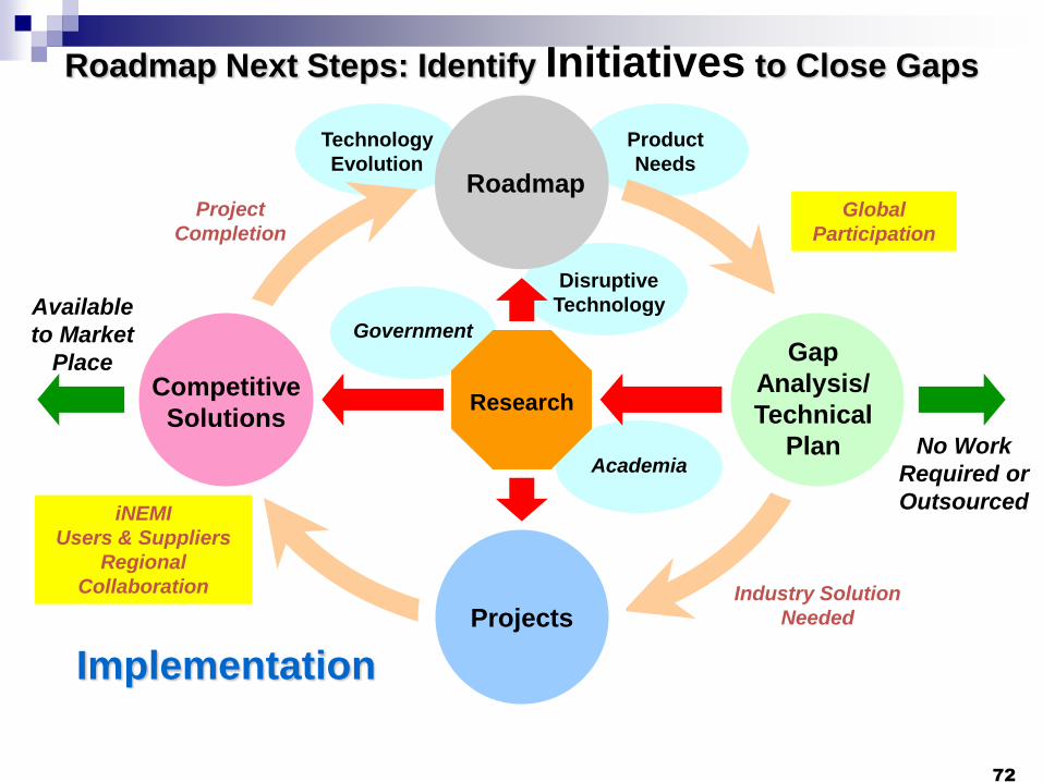
Roadmap
Process &
Scope
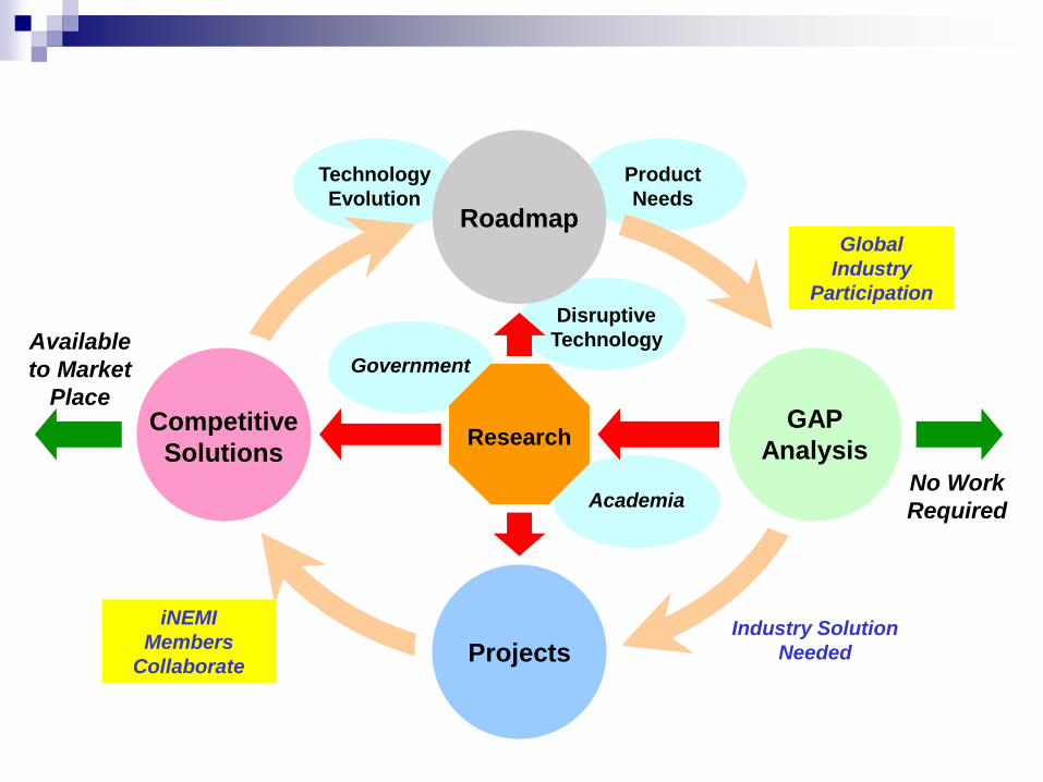
5
Product
Needs
Technology
Evolution
GAP
AnalysisResearch
Projects
Methodology
Competitive
Solutions
Roadmap
Industry Solution
Needed
Academia
Government
iNEMI
Members
Collaborate
No Work
Required
Available
to Market
Place
Global
Industry
Participation Disruptive
Technology
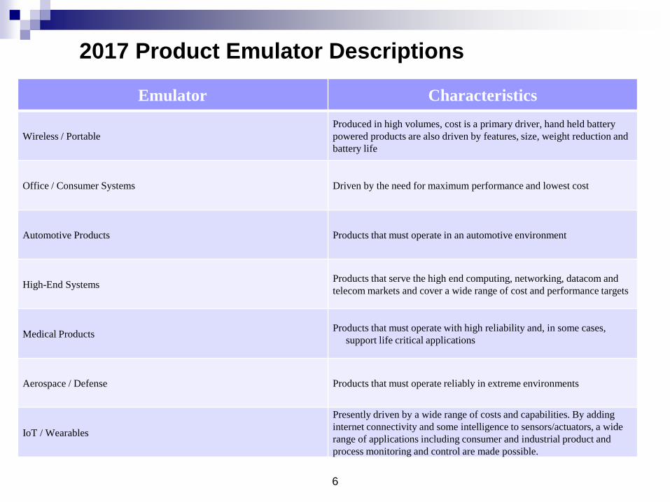
2017 Product Emulator Descriptions
Emulator Characteristics
Wireless / Portable
Produced in high volumes, cost is a primary driver, hand held battery
powered products are also driven by features, size, weight reduction and
battery life
Office / Consumer Systems Driven by the need for maximum performance and lowest cost
Automotive Products Products that must operate in an automotive environment
High-End Systems Products that serve the high end computing, networking, datacom and
telecom markets and cover a wide range of cost and performance targets
Medical ProductsProducts that must operate with high reliability and, in some cases,
support life critical applications
Aerospace / Defense Products that must operate reliably in extreme environments
IoT / Wearables
Presently driven by a wide range of costs and capabilities. By adding
internet connectivity and some intelligence to sensors/actuators, a wide
range of applications including consumer and industrial product and
process monitoring and control are made possible.
6
7
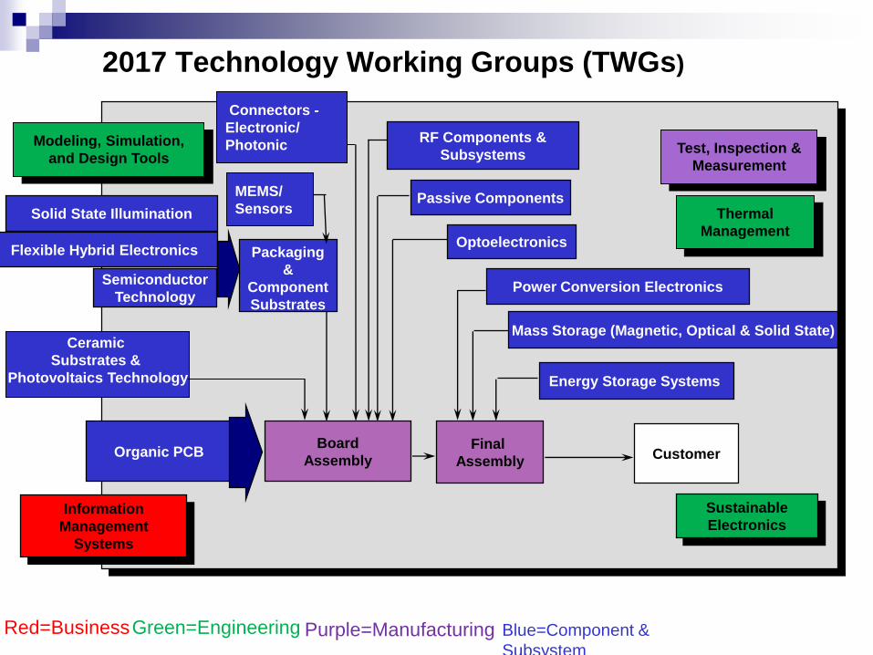
2017 Technology Working Groups (TWGs)
Organic PCBBoard
Assembly Customer
RF Components &
Subsystems
OptoelectronicsFlexible Hybrid Electronics
Energy Storage Systems
Modeling, Simulation,
and Design Tools
Packaging
&
Component
Substrates
Semiconductor
Technology
Final
Assembly
Mass Storage (Magnetic, Optical & Solid State)
Passive Components
Information
Management
Systems
Test, Inspection &
Measurement
Sustainable
Electronics
Ceramic
Substrates &
Photovoltaics Technology
Thermal
Management
Connectors -
Electronic/
Photonic
MEMS/
Sensors
Red=BusinessGreen=Engineering Purple=Manufacturing Blue=Component &
Subsystem
Solid State Illumination
Power Conversion Electronics
Optoelectronics and
Optical Storage
Organic Printed
Circuit Boards
Magnetic and
Optical Storage
Supply Chain
Management
Semiconductors
iNEMI
Information
Management
TWG
iNEMI
Mass Data
Storage TWG
iNEMI / IPC / EIPC
/ TPCA
Organic PWB
TWG
iNEMI / ITRS2.0 /
MIG/PSMA
/IPSR/IRDS/HIR
Packaging
TWG
iNEMI
Board
Assembly
TWG
Interconnect
Substrates—Ceramic
iNEMI Roadmap
iNEMI
Opto-
electronics
TWG
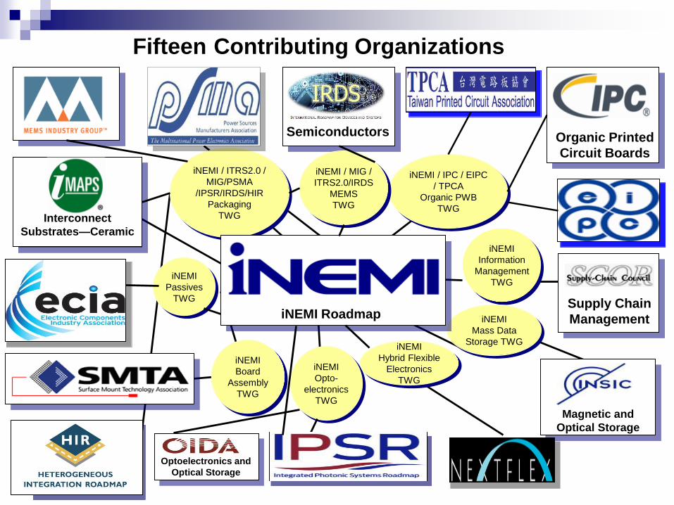
Fifteen Contributing Organizations
iNEMI / MIG /
ITRS2.0/IRDS
MEMS
TWG
iNEMI
Passives
TWG
iNEMI
Hybrid Flexible
Electronics
TWG
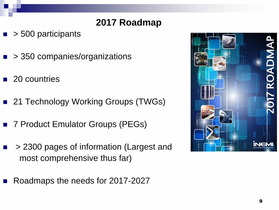
2017 Roadmap
> 500 participants
> 350 companies/organizations
20 countries
21 Technology Working Groups (TWGs)
7 Product Emulator Groups (PEGs)
> 2300 pages of information (Largest and
most comprehensive thus far)
Roadmaps the needs for 2017-2027
9
Technical Plan for Members
5 Year Plan for Implementation
2017
Technical
Plan
(iNEMI Members Only)
• Implementation Plan for Key
Areas
• Key Gaps Prioritized by
TC/TIGs
• Pre-competitive
Collaboration projects/plans
developed by Members
2017 Research Priorities
Chapter 1: Introduction
Chapter 2: Research Needs to support iNEMI
Technology Implementation Groups (TIGs)
and current Projects
Chapter 3: Research Needs For Selected
Enabling Emerging Technologies
Chapter 4: Research Priorities Summarized by
Research Area
Design
Manufacturing Processes
Materials & Reliability
Sustainability
Summary
Appendixes
2017
Research
Priorities
2017 iNEMI
Roadmap
Situation
Analysis
Situation Analysis Examples: Technology Consumers’ demand for thin multifunctional products has led to
increased pressure on alternative high density packaging technologies.
High-density 3D packaging has become the major technology challenge
SiP:
Technology driver for small components, packaging, assembly processes and for high density substrates
New sensors and MEMs:
Expected to see exponential growth driven by portable products
Motion gesture sensors expanding use of 2D-axis & 3D-axis gyroscopes
Segment maturing, encouraging industry collaboration
13
14
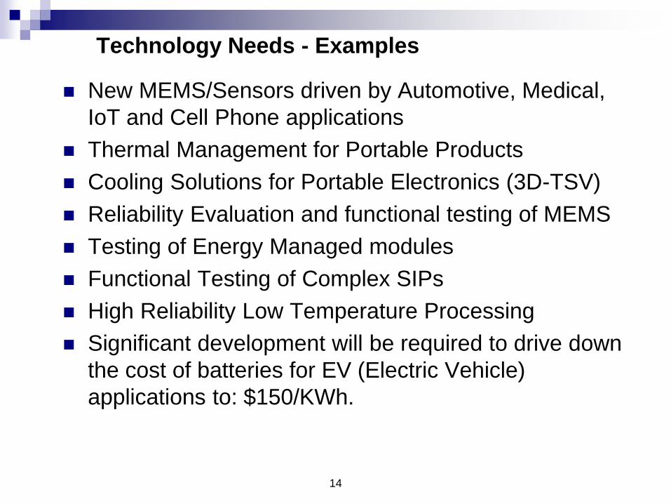
Technology Needs - Examples
New MEMS/Sensors driven by Automotive, Medical,
IoT and Cell Phone applications
Thermal Management for Portable Products
Cooling Solutions for Portable Electronics (3D-TSV)
Reliability Evaluation and functional testing of MEMS
Testing of Energy Managed modules
Functional Testing of Complex SIPs
High Reliability Low Temperature Processing
Significant development will be required to drive down
the cost of batteries for EV (Electric Vehicle)
applications to: $150/KWh.
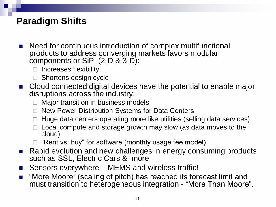
Paradigm Shifts
Need for continuous introduction of complex multifunctional products to address converging markets favors modular components or SiP (2-D & 3-D): Increases flexibility
Shortens design cycle
Cloud connected digital devices have the potential to enable major disruptions across the industry: Major transition in business models
New Power Distribution Systems for Data Centers
Huge data centers operating more like utilities (selling data services)
Local compute and storage growth may slow (as data moves to the cloud)
“Rent vs. buy” for software (monthly usage fee model)
Rapid evolution and new challenges in energy consuming products such as SSL, Electric Cars & more
Sensors everywhere – MEMS and wireless traffic!
“More Moore” (scaling of pitch) has reached its forecast limit and must transition to heterogeneous integration - “More Than Moore”.
15
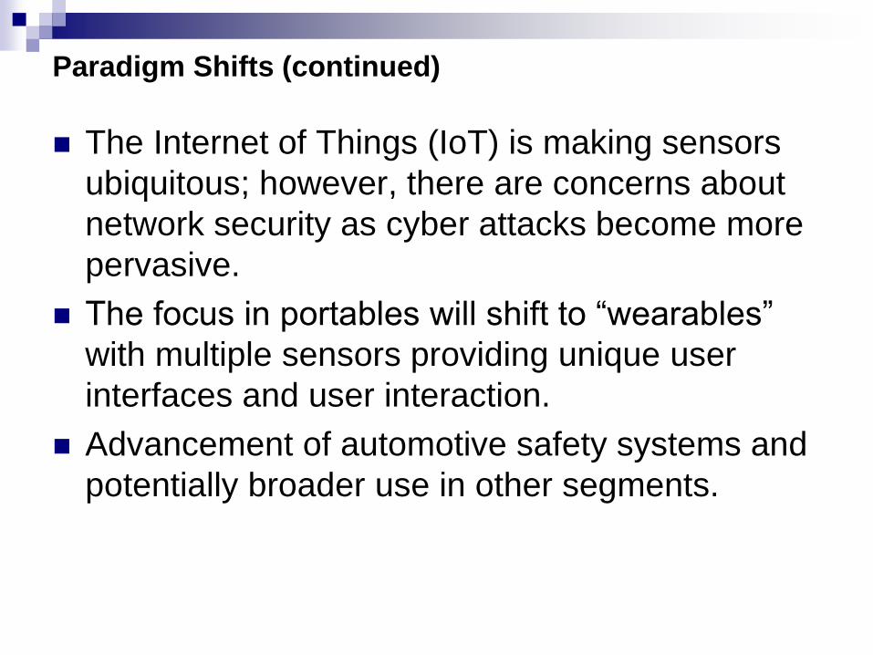
Paradigm Shifts (continued)
The Internet of Things (IoT) is making sensors
ubiquitous; however, there are concerns about
network security as cyber attacks become more
pervasive.
The focus in portables will shift to “wearables”
with multiple sensors providing unique user
interfaces and user interaction.
Advancement of automotive safety systems and
potentially broader use in other segments.
2017 Roadmap IoT/Wearables
Product Sector Highlights
18
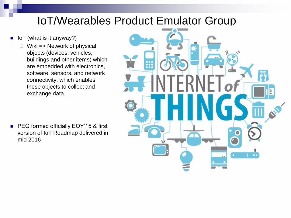
IoT/Wearables Product Emulator Group
IoT (what is it anyway?)
Wiki => Network of physical
objects (devices, vehicles,
buildings and other items) which
are embedded with electronics,
software, sensors, and network
connectivity, which enables
these objects to collect and
exchange data
PEG formed officially EOY’15 & first
version of IoT Roadmap delivered in
mid 2016
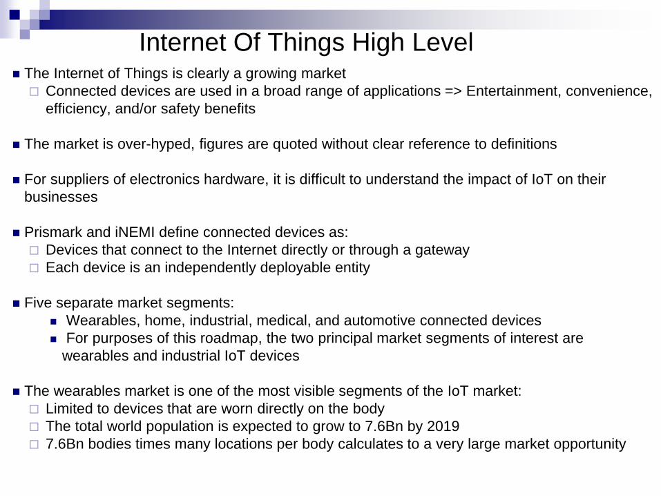
Internet Of Things High Level The Internet of Things is clearly a growing market
Connected devices are used in a broad range of applications => Entertainment, convenience,
efficiency, and/or safety benefits
The market is over-hyped, figures are quoted without clear reference to definitions
For suppliers of electronics hardware, it is difficult to understand the impact of IoT on their
businesses
Prismark and iNEMI define connected devices as:
Devices that connect to the Internet directly or through a gateway
Each device is an independently deployable entity
Five separate market segments:
Wearables, home, industrial, medical, and automotive connected devices
For purposes of this roadmap, the two principal market segments of interest are
wearables and industrial IoT devices
The wearables market is one of the most visible segments of the IoT market:
Limited to devices that are worn directly on the body
The total world population is expected to grow to 7.6Bn by 2019
7.6Bn bodies times many locations per body calculates to a very large market opportunity
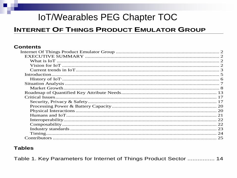
IoT/Wearables PEG Chapter TOC
INTERNET OF THINGS PRODUCT EMULATOR GROUP
Contents
Internet Of Things Product Emulator Group ............................................................................. 2
EXECUTIVE SUMMARY .................................................................................................... 2
What is IoT ......................................................................................................................... 2
Vision for IoT ..................................................................................................................... 2
Current trends in IoT ........................................................................................................... 3
Introduction ............................................................................................................................. 5
History of IoT, ..................................................................................................................... 6
Situation Analysis ................................................................................................................... 7
Market Growth .................................................................................................................... 8
Roadmap of Quantified Key Attribute Needs ....................................................................... 13
Critical Issues ........................................................................................................................ 17
Security, Privacy & Safety ................................................................................................ 17
Processing Power & Battery Capacity .............................................................................. 20
Physical Interactions ......................................................................................................... 20
Humans and IoT ................................................................................................................ 21
Interoperability .................................................................................................................. 22
Composability ................................................................................................................... 22
Industry standards ............................................................................................................. 23
Timing ............................................................................................................................... 24
Contributors .......................................................................................................................... 25
Tables Table 1. Key Parameters for Internet of Things Product Sector ................ 14
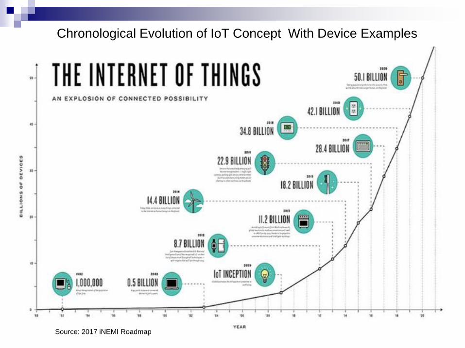
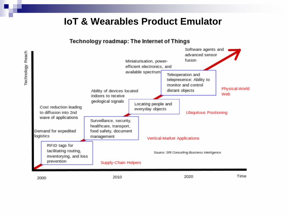
Chronological Evolution of IoT Concept With Device Examples
Source: 2017 iNEMI Roadmap

Useful/Actionable Data Gathering

World On A Laptop
Mobile devices along with connectivity revolutionized our way of interaction
IoT & Wearables Product Emulator
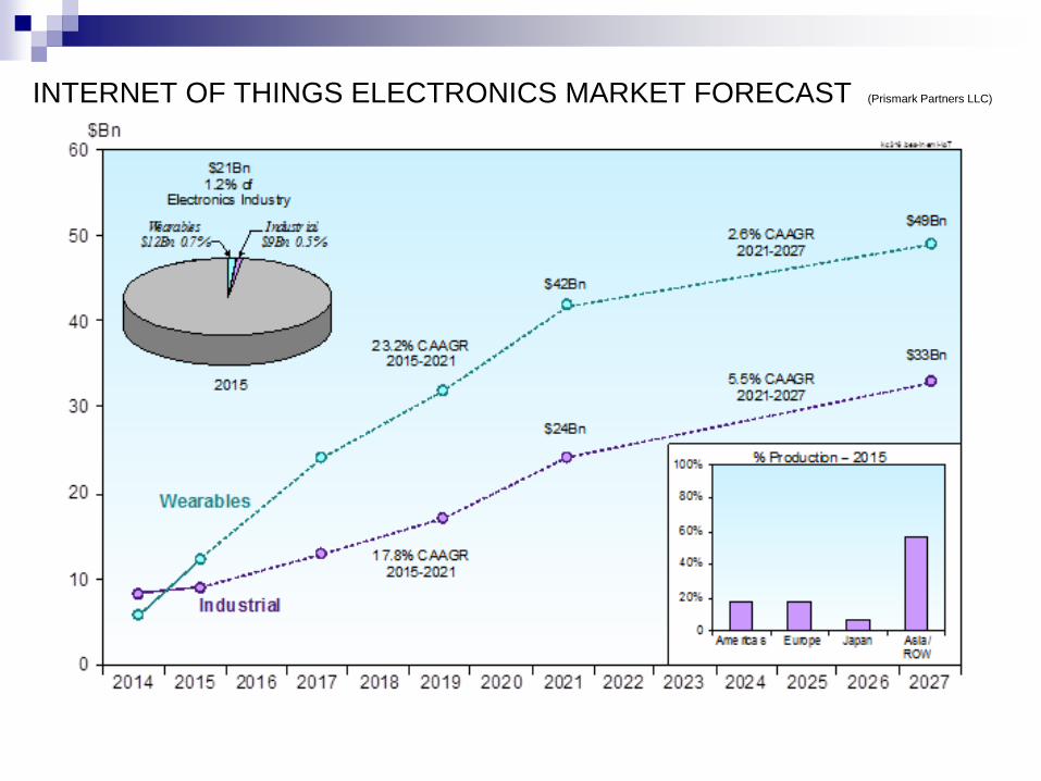
INTERNET OF THINGS ELECTRONICS MARKET FORECAST (Prismark Partners LLC)
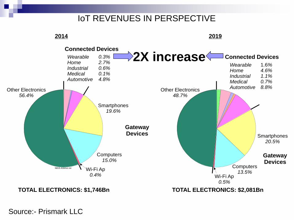
WearableHome IndustrialMedicalAutomotive
Wearable Home IndustrialMedicalAutomotive
Smartphones19.6%
Smartphones20.5%
Computers15.0%
Computers13.5%
Other Electronics56.4%
Other Electronics48.7%
Wi-Fi Ap0.4%
N815.416mvc-iot
Wi-Fi Ap0.5%
0.3%2.7%0.6%0.1%4.8%
1.6%4.6%1.1%0.7%8.8%
Connected Devices
Connected Devices
2014 2019
TOTAL ELECTRONICS: $1,746Bn
IoT REVENUES IN PERSPECTIVE
TOTAL ELECTRONICS: $2,081Bn
GatewayDevices
GatewayDevices
Source:- Prismark LLC
2X increase
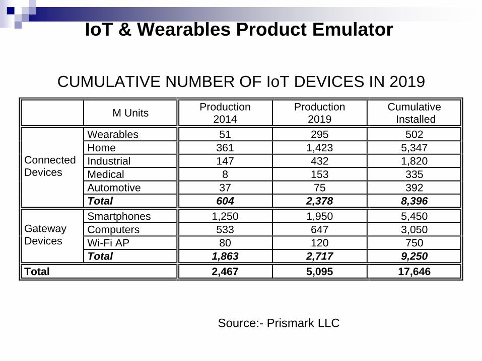
CUMULATIVE NUMBER OF IoT DEVICES IN 2019
M Units
Production 2014
Production 2019
Cumulative Installed
Wearables 51 295 502
Home 361 1,423 5,347
Industrial 147 432 1,820
Medical 8 153 335
Automotive 37 75 392
Connected Devices
Total 604 2,378 8,396
Smartphones 1,250 1,950 5,450
Computers 533 647 3,050
Wi-Fi AP 80 120 750
Gateway Devices
Total 1,863 2,717 9,250
Total 2,467 5,095 17,646
Source:- Prismark LLC
IoT & Wearables Product Emulator
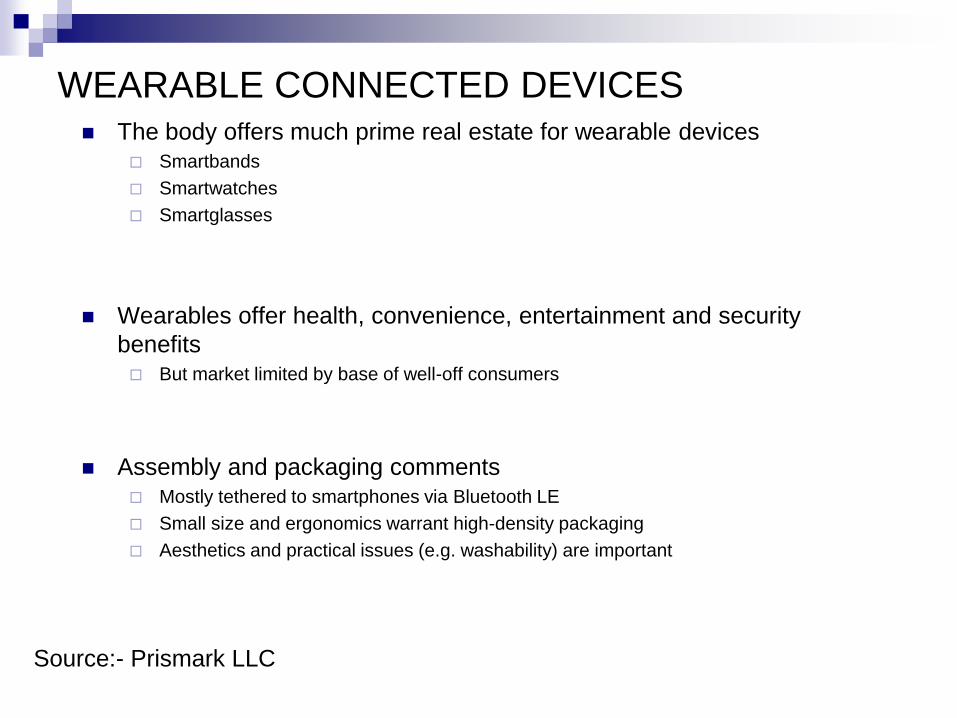
WEARABLE CONNECTED DEVICES The body offers much prime real estate for wearable devices
Smartbands
Smartwatches
Smartglasses
Wearables offer health, convenience, entertainment and security
benefits But market limited by base of well-off consumers
Assembly and packaging comments Mostly tethered to smartphones via Bluetooth LE
Small size and ergonomics warrant high-density packaging
Aesthetics and practical issues (e.g. washability) are important
Source:- Prismark LLC
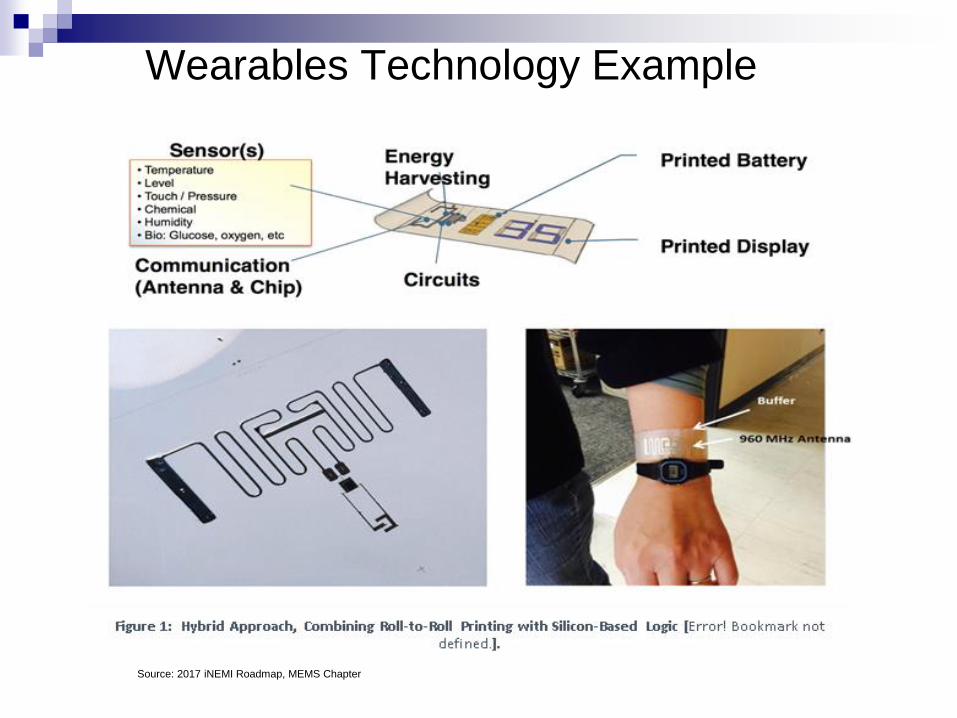
Wearables Technology Example
Source: 2017 iNEMI Roadmap, MEMS Chapter
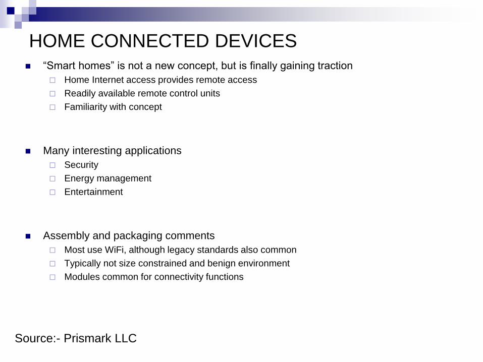
HOME CONNECTED DEVICES “Smart homes” is not a new concept, but is finally gaining traction
Home Internet access provides remote access
Readily available remote control units
Familiarity with concept
Many interesting applications
Security
Energy management
Entertainment
Assembly and packaging comments
Most use WiFi, although legacy standards also common
Typically not size constrained and benign environment
Modules common for connectivity functions
Source:- Prismark LLC
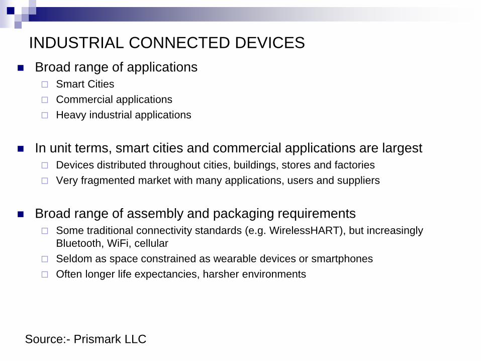
INDUSTRIAL CONNECTED DEVICES
Broad range of applications
Smart Cities
Commercial applications
Heavy industrial applications
In unit terms, smart cities and commercial applications are largest
Devices distributed throughout cities, buildings, stores and factories
Very fragmented market with many applications, users and suppliers
Broad range of assembly and packaging requirements
Some traditional connectivity standards (e.g. WirelessHART), but increasingly
Bluetooth, WiFi, cellular
Seldom as space constrained as wearable devices or smartphones
Often longer life expectancies, harsher environments
Source:- Prismark LLC
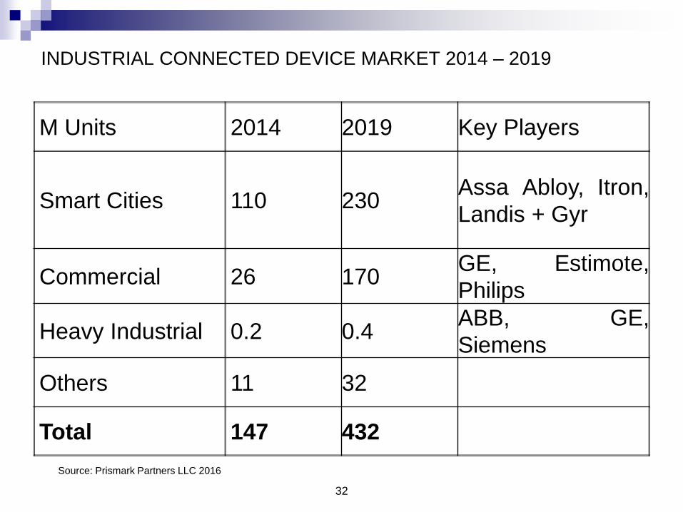
INDUSTRIAL CONNECTED DEVICE MARKET 2014 – 2019
M Units 2014 2019 Key Players
Smart Cities 110 230Assa Abloy, Itron,
Landis + Gyr
Commercial 26 170GE, Estimote,
Philips
Heavy Industrial 0.2 0.4ABB, GE,
Siemens
Others 11 32
Total 147 432
32
Source: Prismark Partners LLC 2016
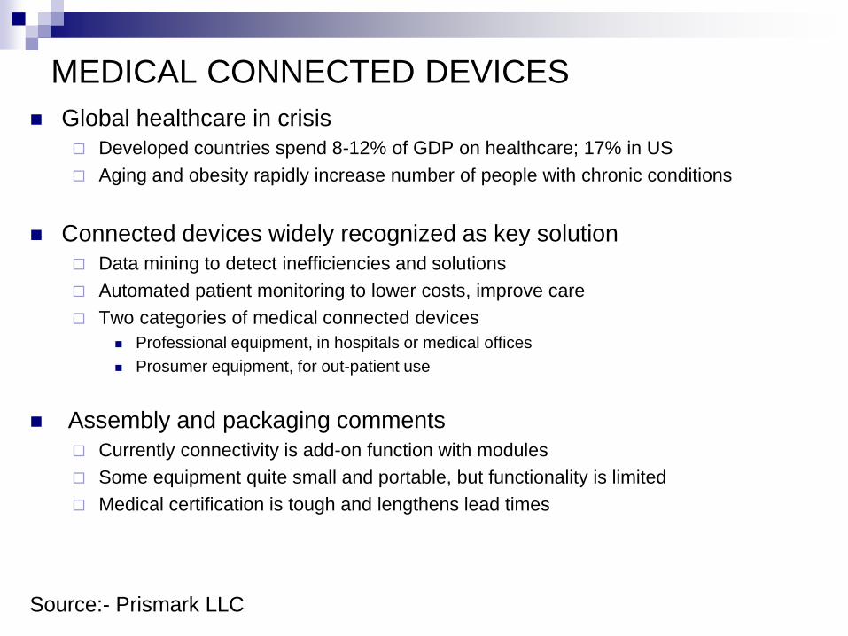
MEDICAL CONNECTED DEVICES
Global healthcare in crisis
Developed countries spend 8-12% of GDP on healthcare; 17% in US
Aging and obesity rapidly increase number of people with chronic conditions
Connected devices widely recognized as key solution
Data mining to detect inefficiencies and solutions
Automated patient monitoring to lower costs, improve care
Two categories of medical connected devices
Professional equipment, in hospitals or medical offices
Prosumer equipment, for out-patient use
Assembly and packaging comments
Currently connectivity is add-on function with modules
Some equipment quite small and portable, but functionality is limited
Medical certification is tough and lengthens lead times
Source:- Prismark LLC
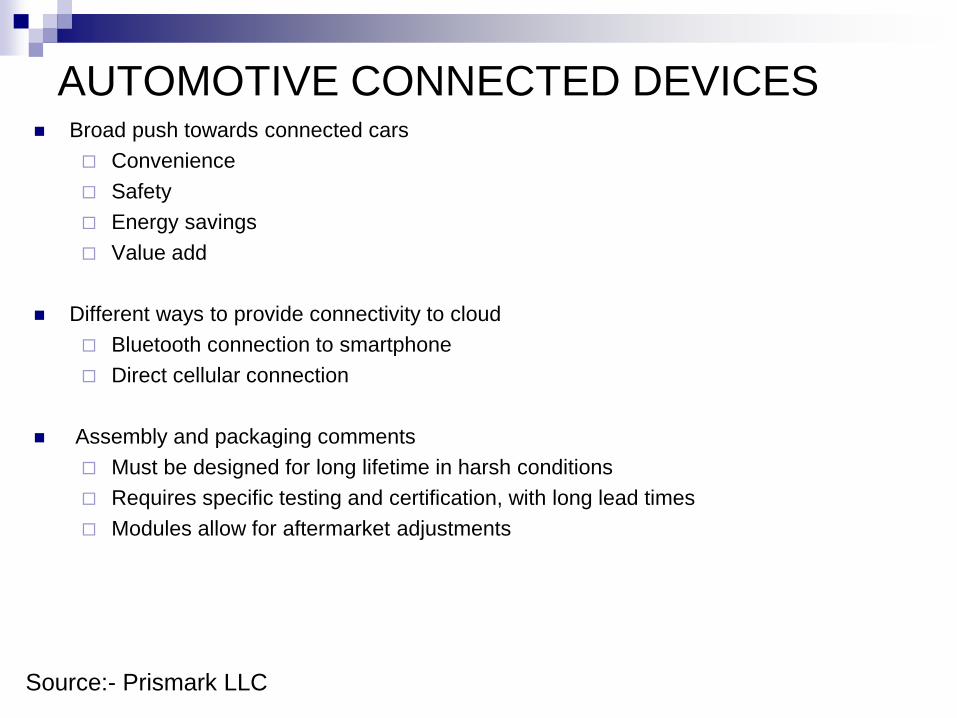
AUTOMOTIVE CONNECTED DEVICES Broad push towards connected cars
Convenience
Safety
Energy savings
Value add
Different ways to provide connectivity to cloud
Bluetooth connection to smartphone
Direct cellular connection
Assembly and packaging comments
Must be designed for long lifetime in harsh conditions
Requires specific testing and certification, with long lead times
Modules allow for aftermarket adjustments
Source:- Prismark LLC
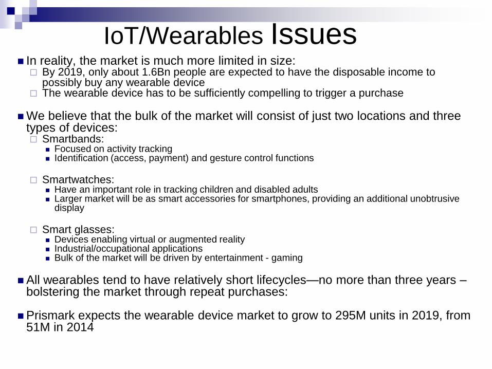
IoT/Wearables Issues In reality, the market is much more limited in size: By 2019, only about 1.6Bn people are expected to have the disposable income to
possibly buy any wearable device The wearable device has to be sufficiently compelling to trigger a purchase
We believe that the bulk of the market will consist of just two locations and three types of devices: Smartbands:
Focused on activity tracking Identification (access, payment) and gesture control functions
Smartwatches: Have an important role in tracking children and disabled adults Larger market will be as smart accessories for smartphones, providing an additional unobtrusive
display
Smart glasses: Devices enabling virtual or augmented reality Industrial/occupational applications Bulk of the market will be driven by entertainment - gaming
All wearables tend to have relatively short lifecycles—no more than three years –bolstering the market through repeat purchases:
Prismark expects the wearable device market to grow to 295M units in 2019, from 51M in 2014
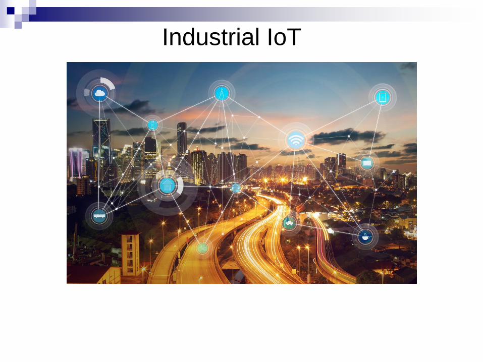
Industrial IoT
IoT / Industrial Issues Industrial applications offer a broad range of opportunities for connected devicesUse cases and implementations are just as broad
Prismark/iNEMI divide the market into four specific segments: “Smart Cities”, “Commercial Applications,” “Heavy Industrial”, and one “other” category
The industrial connected device is specified, purchased, and deployed by a corporation, government authority, or other institution with expected longer lifetimes, sometimes ten or more years in a harsh environment.
Industrial ContinuedSmart Cities:
Cities with large populations (or densities) need to be managed carefully; otherwise, the quality of life degrades quickly.
The single largest industrial connected device category today is smart meters: Meter reading becomes even more efficient because it is now completely remote Second, the meter can be read at any time interval, even continuously, which allows for
sophisticated pricing models
Another priority for smart cities is lighting management: Ranges from in-building to street lights to traffic lights LED bulbs with integrated links (wired, wireless, network), e.g. ZigBee, are widely available for
indoor and outdoor applications
Energy management in buildings also requires tight control over the HVAC system Individual thermostats are fitted with modules that allow remote monitoring and control
IoT / Industrial Issues (2)
Commercial Connected Devices:
Companies use connected devices in their factories or
stores for energy management systems including lighting
and HVAC control
Additionally, the commercial sector has other specific IoT applications that are of interest:
Beacons - can be used for proximity sensing - a shoe store
may alert a smartphone user of a shoe store when the
user passes by
Sensors to increase efficiency or ensure safety
Sensors networked to allow for remote monitoring
Enables centralized data collection
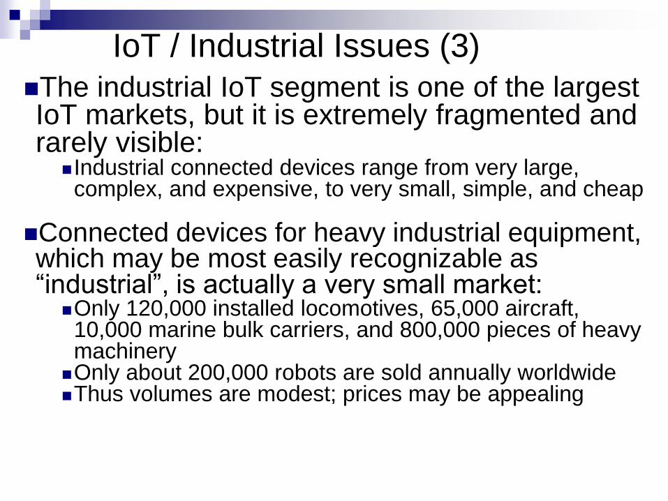
IoT / Industrial Issues (3)
The industrial IoT segment is one of the largest IoT markets, but it is extremely fragmented and rarely visible:
Industrial connected devices range from very large, complex, and expensive, to very small, simple, and cheap
Connected devices for heavy industrial equipment, which may be most easily recognizable as “industrial”, is actually a very small market:
Only 120,000 installed locomotives, 65,000 aircraft, 10,000 marine bulk carriers, and 800,000 pieces of heavy machinery
Only about 200,000 robots are sold annually worldwide Thus volumes are modest; prices may be appealing
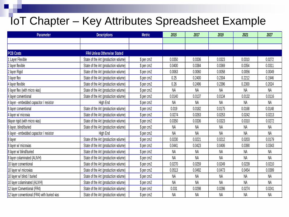
IoT Chapter – Key Attributes Spreadsheet ExampleParameter Descriptions Metric 2015 2017 2019 2021 2027
PCB Costs FR4 Unless Otherwise Stated
1 Layer Flexible State of the Art (production volume) $ per cm2 0.0350 0.0336 0.0323 0.0310 0.0272
2 layer flexible State of the Art (production volume) $ per cm2 0.0400 0.0384 0.0369 0.0354 0.0311
2 layer Rigid State of the Art (production volume) $ per cm2 0.0063 0.0060 0.0058 0.0056 0.0049
3 layer flex State of the Art (production volume) $ per cm2 0.25 0.2400 0.2304 0.2212 0.1946
4 layer flexible State of the Art (production volume) $ per cm2 0.26 0.2496 0.2396 0.2300 0.2024
6 layer flex (with micro vias) State of the Art (production volume) $ per cm2 NA NA NA NA NA
4 layer conventional State of the Art (production volume) $ per cm2 0.0140 0.0137 0.0134 0.0132 0.0116
4 layer - embedded capacitor / resistor High End $ per cm2 NA NA NA NA NA
6 layer conventional State of the Art (production volume) $ per cm2 0.019 0.0182 0.0175 0.0168 0.0148
4 layer w/ microvia State of the Art (production volume) $ per cm2 0.0274 0.0263 0.0253 0.0242 0.0213
6layer rigid (with micro vias) State of the Art (production volume) $ per cm2 0.0350 0.0336 0.0323 0.0310 0.0272
6 layer, blind/buried State of the Art (production volume) $ per cm2 NA NA NA NA NA
6 layer - embedded capacitor / resistor High End $ per cm2 NA NA NA NA NA
8 layer State of the Art (production volume) $ per cm2 0.0230 0.0221 0.0212 0.0203 0.0179
8 layer w/ microvias State of the Art (production volume) $ per cm2 0.0441 0.0423 0.0406 0.0390 0.0343
8 layer w/ blind/buried State of the Art (production volume) $ per cm2 NA NA NA NA NA
8 layer colaminated (ALIVH) State of the Art (production volume) $ per cm2 NA NA NA NA NA
10 layer conventional State of the Art (production volume) $ per cm2 0.0270 0.0259 0.0249 0.0239 0.0210
10 layer w/ microvias State of the Art (production volume) $ per cm2 0.0513 0.0492 0.0473 0.0454 0.0399
10 layer w/ blind / buried State of the Art (production volume) $ per cm2 NA NA NA NA NA
10 layer colaminated (ALIVH) State of the Art (production volume) $ per cm2 NA NA NA NA NA
12 layer Conventional (FR4) State of the Art (production volume) $ per cm2 0.031 0.0298 0.0286 0.0274 0.0241
12 layer conventional (FR4) with buried vias State of the Art (production volume) $ per cm2 NA NA NA NA NA
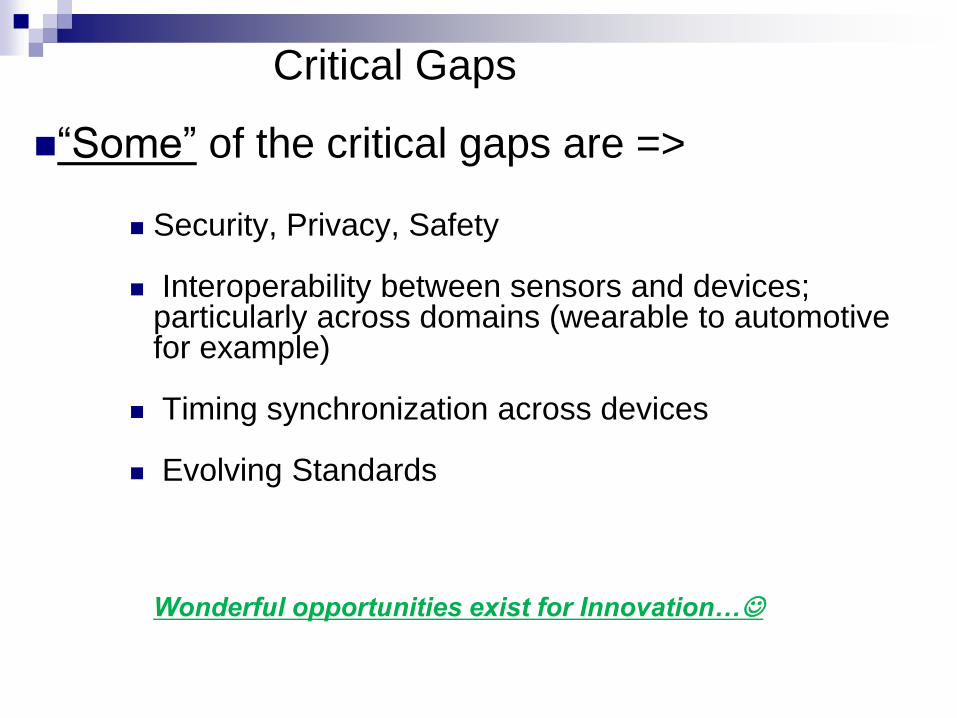
Critical Gaps
“Some” of the critical gaps are =>
Security, Privacy, Safety
Interoperability between sensors and devices; particularly across domains (wearable to automotive for example)
Timing synchronization across devices
Evolving Standards
Wonderful opportunities exist for Innovation…☺

2017 Roadmap
Board Assembly
TWG Chapter
Highlights
44
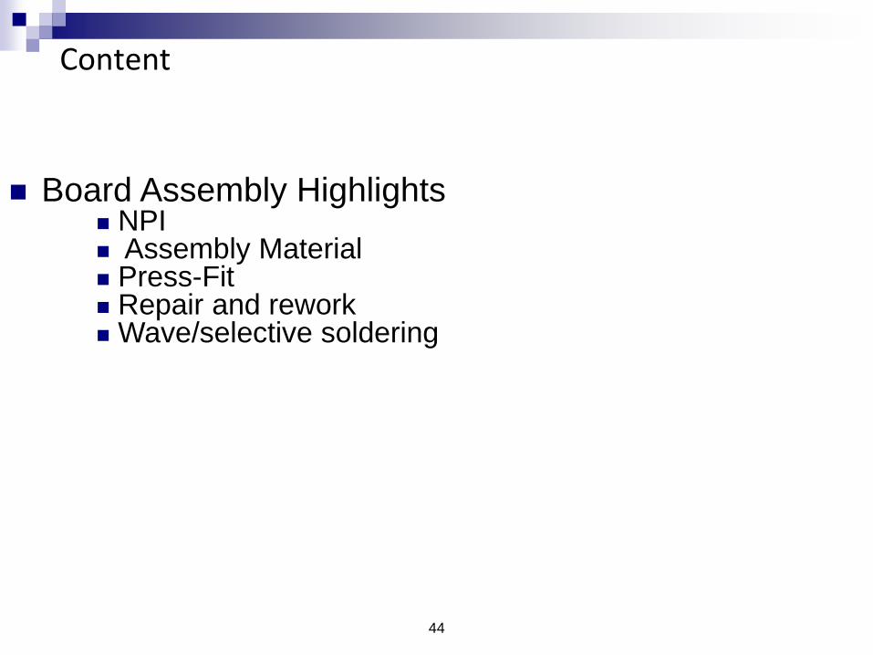
Content
Board Assembly Highlights NPI Assembly Material Press-Fit Repair and rework Wave/selective soldering
New Product Introduction Section
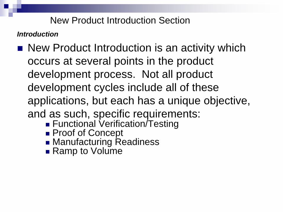
Introduction
New Product Introduction is an activity which
occurs at several points in the product
development process. Not all product
development cycles include all of these
applications, but each has a unique objective,
and as such, specific requirements: Functional Verification/Testing Proof of Concept Manufacturing Readiness Ramp to Volume
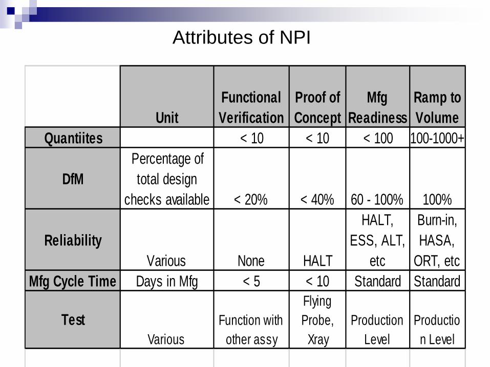
Attributes of NPI
Unit
Functional
Verification
Proof of
Concept
Mfg
Readiness
Ramp to
Volume
Quantiites < 10 < 10 < 100 100-1000+
DfM
Percentage of
total design
checks available < 20% < 40% 60 - 100% 100%
Reliability
Various None HALT
HALT,
ESS, ALT,
etc
Burn-in,
HASA,
ORT, etc
Mfg Cycle Time Days in Mfg < 5 < 10 Standard Standard
Test
Various
Function with
other assy
Flying
Probe,
Xray
Production
Level
Productio
n Level
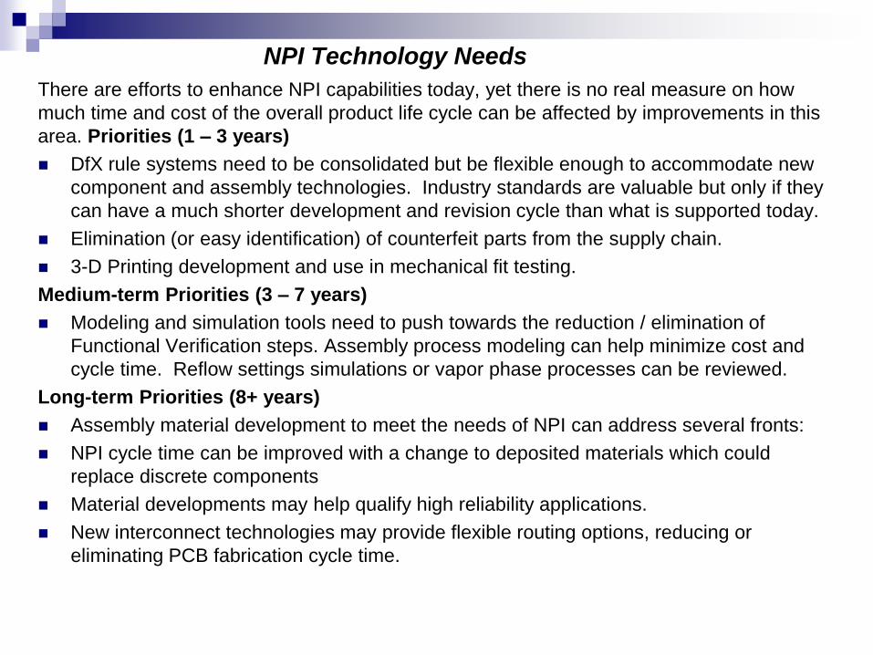
NPI Technology Needs
There are efforts to enhance NPI capabilities today, yet there is no real measure on how
much time and cost of the overall product life cycle can be affected by improvements in this
area. Priorities (1 – 3 years)
DfX rule systems need to be consolidated but be flexible enough to accommodate new
component and assembly technologies. Industry standards are valuable but only if they
can have a much shorter development and revision cycle than what is supported today.
Elimination (or easy identification) of counterfeit parts from the supply chain.
3-D Printing development and use in mechanical fit testing.
Medium-term Priorities (3 – 7 years)
Modeling and simulation tools need to push towards the reduction / elimination of
Functional Verification steps. Assembly process modeling can help minimize cost and
cycle time. Reflow settings simulations or vapor phase processes can be reviewed.
Long-term Priorities (8+ years)
Assembly material development to meet the needs of NPI can address several fronts:
NPI cycle time can be improved with a change to deposited materials which could
replace discrete components
Material developments may help qualify high reliability applications.
New interconnect technologies may provide flexible routing options, reducing or
eliminating PCB fabrication cycle time.
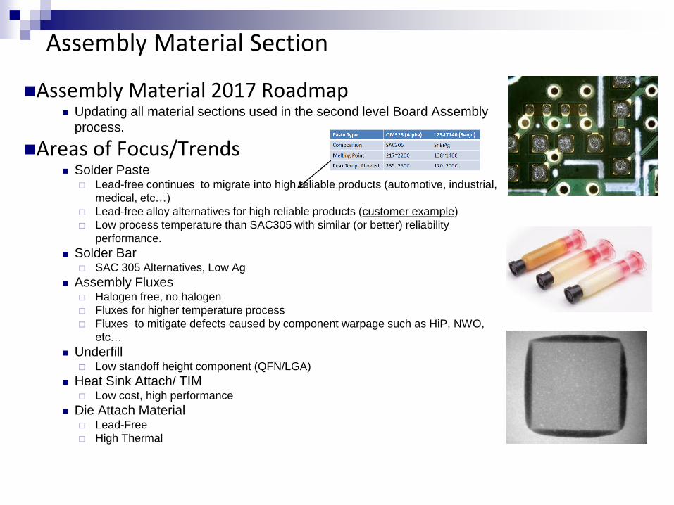
Assembly Material Section
Assembly Material 2017 Roadmap Updating all material sections used in the second level Board Assembly
process.
Areas of Focus/Trends Solder Paste
Lead-free continues to migrate into high reliable products (automotive, industrial,
medical, etc…)
Lead-free alloy alternatives for high reliable products (customer example)
Low process temperature than SAC305 with similar (or better) reliability
performance.
Solder Bar SAC 305 Alternatives, Low Ag
Assembly Fluxes Halogen free, no halogen
Fluxes for higher temperature process
Fluxes to mitigate defects caused by component warpage such as HiP, NWO,
etc…
Underfill Low standoff height component (QFN/LGA)
Heat Sink Attach/ TIM Low cost, high performance
Die Attach Material Lead-Free
High Thermal
Assembly Material
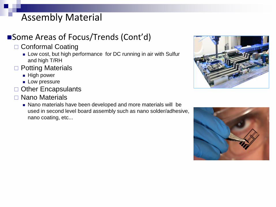
Some Areas of Focus/Trends (Cont’d) Conformal Coating
Low cost, but high performance for DC running in air with Sulfur
and high T/RH
Potting Materials High power
Low pressure
Other Encapsulants
Nano Materials Nano materials have been developed and more materials will be
used in second level board assembly such as nano solder/adhesive,
nano coating, etc...
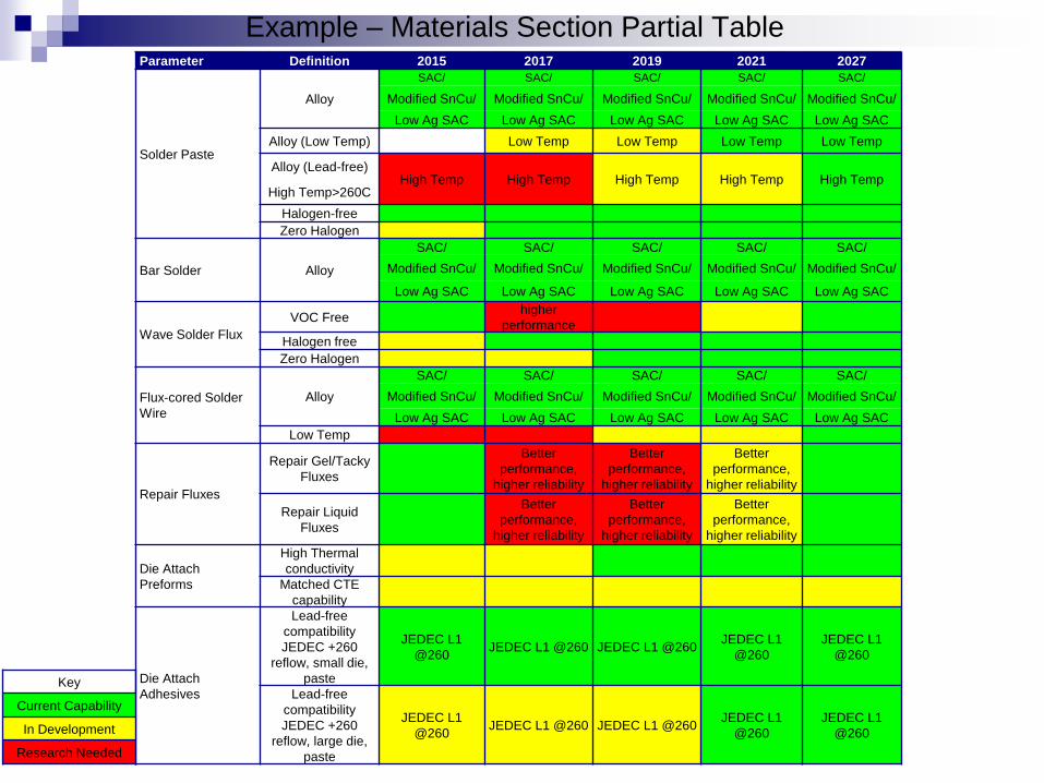
Example – Materials Section Partial TableParameter Definition 2015 2017 2019 2021 2027
Solder Paste
Alloy
SAC/ SAC/ SAC/ SAC/ SAC/
Modified SnCu/ Modified SnCu/ Modified SnCu/ Modified SnCu/ Modified SnCu/
Low Ag SAC Low Ag SAC Low Ag SAC Low Ag SAC Low Ag SAC
Alloy (Low Temp) Low Temp Low Temp Low Temp Low Temp
Alloy (Lead-free)High Temp High Temp High Temp High Temp High Temp
High Temp>260C
Halogen-free
Zero Halogen
Bar Solder Alloy
SAC/ SAC/ SAC/ SAC/ SAC/
Modified SnCu/ Modified SnCu/ Modified SnCu/ Modified SnCu/ Modified SnCu/
Low Ag SAC Low Ag SAC Low Ag SAC Low Ag SAC Low Ag SAC
Wave Solder Flux
VOC Freehigher
performance
Halogen free
Zero Halogen
Flux-cored Solder
Wire
Alloy
SAC/ SAC/ SAC/ SAC/ SAC/
Modified SnCu/ Modified SnCu/ Modified SnCu/ Modified SnCu/ Modified SnCu/
Low Ag SAC Low Ag SAC Low Ag SAC Low Ag SAC Low Ag SAC
Low Temp
Repair Fluxes
Repair Gel/Tacky
Fluxes
Better
performance,
higher reliability
Better
performance,
higher reliability
Better
performance,
higher reliability
Repair Liquid
Fluxes
Better
performance,
higher reliability
Better
performance,
higher reliability
Better
performance,
higher reliability
Die Attach
Preforms
High Thermal
conductivity
Matched CTE
capability
Die Attach
Adhesives
Lead-free
compatibility
JEDEC +260
reflow, small die,
paste
JEDEC L1
@260JEDEC L1 @260 JEDEC L1 @260
JEDEC L1
@260
JEDEC L1
@260
Lead-free
compatibility
JEDEC +260
reflow, large die,
paste
JEDEC L1
@260JEDEC L1 @260 JEDEC L1 @260
JEDEC L1
@260
JEDEC L1
@260
Key
Current Capability
In Development
Research Needed
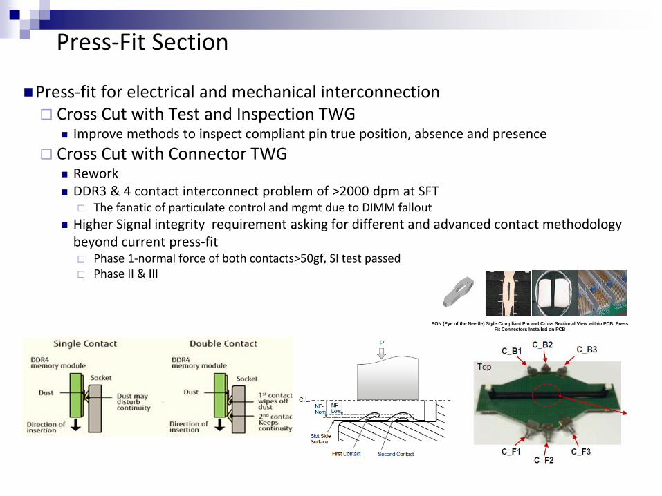
Press-Fit Section
Press-fit for electrical and mechanical interconnection Cross Cut with Test and Inspection TWG
Improve methods to inspect compliant pin true position, absence and presence
Cross Cut with Connector TWG Rework DDR3 & 4 contact interconnect problem of >2000 dpm at SFT
The fanatic of particulate control and mgmt due to DIMM fallout
Higher Signal integrity requirement asking for different and advanced contact methodology beyond current press-fit Phase 1-normal force of both contacts>50gf, SI test passed Phase II & III
EON (Eye of the Needle) Style Compliant Pin and Cross Sectional View within PCB. Press Fit Connectors Installed on PCB
Rework and Repair Section - Situation Analysis
The roadmap analysis for the repair and rework processes consist of hand soldering repair,PTH rework, SMT rework, and press-fit rework.
The higher lead-free process temperatures forecast by all the product sectors will narrowthe process window for rework (except press-fit).
The selection of a common industry lead-free alloy for both SMT and PTH soldering hasyet to be defined. Many variations of the SnAgCu and SnCu alloys are available for use.
With this variation comes a continued requirement for understanding the quality andreliability of each alloy as well as the combination of alloys, through mixed reworkscenarios.
The trend toward tighter component pitches has required increased component placementaccuracy for rework. High component pin counts and larger component body sizes willchallenge current rework placement and reflow techniques and impact rework yields.
For leadless device rework the lack of “affordable”, capable x-ray capabilities to discern mirrored devices without destructive means is critical for widespread rework capacity.
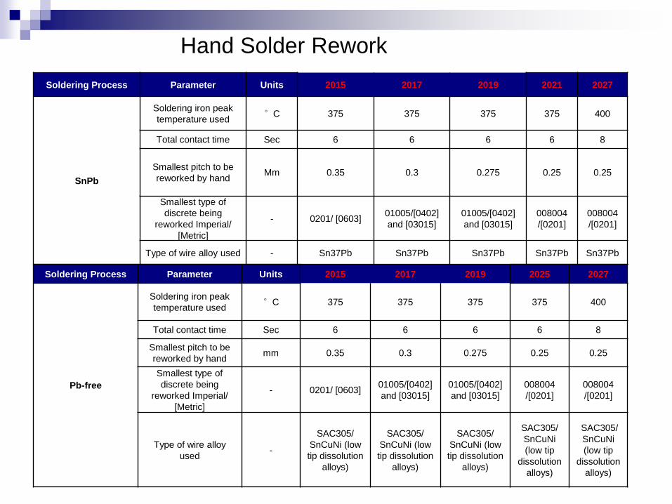
Hand Solder Rework
Soldering Process Parameter Units 2015 2017 2019 2021 2027
SnPb
Soldering iron peak
temperature used°C 375 375 375 375 400
Total contact time Sec 6 6 6 6 8
Smallest pitch to be
reworked by handMm 0.35 0.3 0.275 0.25 0.25
Smallest type of
discrete being
reworked Imperial/
[Metric]
- 0201/ [0603]01005/[0402]
and [03015]
01005/[0402]
and [03015]
008004
/[0201]
008004
/[0201]
Type of wire alloy used - Sn37Pb Sn37Pb Sn37Pb Sn37Pb Sn37Pb
Soldering Process Parameter Units 2015 2017 2019 2025 2027
Pb-free
Soldering iron peak
temperature used°C 375 375 375 375 400
Total contact time Sec 6 6 6 6 8
Smallest pitch to be
reworked by handmm 0.35 0.3 0.275 0.25 0.25
Smallest type of
discrete being
reworked Imperial/
[Metric]
- 0201/ [0603]01005/[0402]
and [03015]
01005/[0402]
and [03015]
008004
/[0201]
008004
/[0201]
Type of wire alloy
used-
SAC305/
SnCuNi (low
tip dissolution
alloys)
SAC305/
SnCuNi (low
tip dissolution
alloys)
SAC305/
SnCuNi (low
tip dissolution
alloys)
SAC305/
SnCuNi
(low tip
dissolution
alloys)
SAC305/
SnCuNi
(low tip
dissolution
alloys)
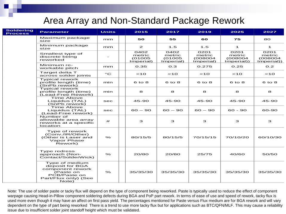
Area Array and Non-Standard Package ReworkSoldering Process
Parameter Units 2015 2017 2019 2025 2027
Maximum package size
mm 50 55 60 75 80
Minimum package size
mm 2 1.5 1.5 1 1
Smallest type of discrete being reworked
-
0402 metric (01005
Imperial)
0402 metric (01005
Imperial)
0201 metric
(008004 Imperial)
0201 metric
(008004 Imperial))
0201 metric
(008004 Imperial))
Minimum re-workable pitch
mm 0.35 0.3 0.275 0.25 0.2
Target delta T across solder joints
°C <10 <10 <10 <10 <10
Typical rework profile length (time) (SnPb rework)
min 6 to 8 6 to 8 6 to 8 6 to 8 6 to 8
Typical rework profile length (time) (Lead-Free Rework)
min 8 8 8 8 8
Time Above Liquidus (TAL) (SnPb rework)
sec 45-90 45-90 45-90 45-90 45-90
Time Above Liquidus (TAL)
(Lead-Free rework) sec 60 – 90 60 – 90 60 – 90 60 - 90 60-90
Number of allowable area array reworks at a specific location
# 3 3 3 3 3
Type of rework (Conv./IR/Other)
(Other is Laser and Vapor Phase
Rework)
% 80/15/5 80/15/5 70/15/15 70/10/20 60/10/30
Type redress approach (Non-Contact/SolderWick)
% 20/80 20/80 25/75 40/60 50/50
Type of medium deposit for BGA
component rework (Paste on
PCB/Paste on Part/Flux only) (See
Note)
% 35/35/30 35/35/30 35/35/30 35/35/30 35/35/30
Note: The use of solder paste or tacky flux will depend on the type of component being reworked. Paste is typically used to reduce the effect of component
warpage causing Head-in-Pillow component soldering defects during BGA and PoP part rework. In terms of ease of use and speed of rework, tacky flux is
used more even though it may have an affect on first pass yield. The percentages mentioned for Paste versus Flux medium are for BGA rework and will vary
dependent on the type of part being reworked. There is a trend to use more tacky flux but for applications such as BTC/QFN/MLF. This may cause a reliability
issue due to insufficient solder joint standoff height which must be validated.
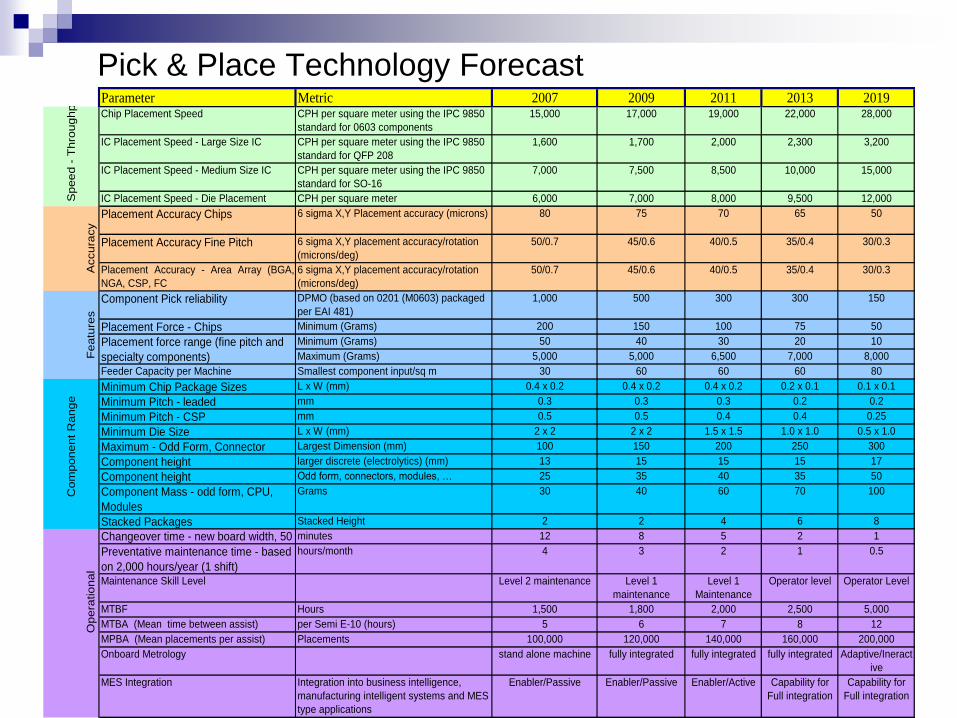
Pick & Place Technology Forecast Parameter Metric 2007 2009 2011 2013 2019Chip Placement Speed CPH per square meter using the IPC 9850
standard for 0603 components
15,000 17,000 19,000 22,000 28,000
IC Placement Speed - Large Size IC CPH per square meter using the IPC 9850
standard for QFP 208
1,600 1,700 2,000 2,300 3,200
IC Placement Speed - Medium Size IC CPH per square meter using the IPC 9850
standard for SO-16
7,000 7,500 8,500 10,000 15,000
IC Placement Speed - Die Placement CPH per square meter 6,000 7,000 8,000 9,500 12,000
Placement Accuracy Chips 6 sigma X,Y Placement accuracy (microns) 80 75 70 65 50
Placement Accuracy Fine Pitch 6 sigma X,Y placement accuracy/rotation
(microns/deg)
50/0.7 45/0.6 40/0.5 35/0.4 30/0.3
Placement Accuracy - Area Array (BGA,
NGA, CSP, FC
6 sigma X,Y placement accuracy/rotation
(microns/deg)
50/0.7 45/0.6 40/0.5 35/0.4 30/0.3
Component Pick reliability DPMO (based on 0201 (M0603) packaged
per EAI 481)
1,000 500 300 300 150
Placement Force - Chips Minimum (Grams) 200 150 100 75 50
Minimum (Grams) 50 40 30 20 10
Maximum (Grams) 5,000 5,000 6,500 7,000 8,000
Feeder Capacity per Machine Smallest component input/sq m 30 60 60 60 80
Minimum Chip Package Sizes L x W (mm) 0.4 x 0.2 0.4 x 0.2 0.4 x 0.2 0.2 x 0.1 0.1 x 0.1
Minimum Pitch - leaded mm 0.3 0.3 0.3 0.2 0.2
Minimum Pitch - CSP mm 0.5 0.5 0.4 0.4 0.25
Minimum Die Size L x W (mm) 2 x 2 2 x 2 1.5 x 1.5 1.0 x 1.0 0.5 x 1.0
Maximum - Odd Form, Connector Largest Dimension (mm) 100 150 200 250 300
Component height larger discrete (electrolytics) (mm) 13 15 15 15 17
Component height Odd form, connectors, modules, … 25 35 40 35 50
Component Mass - odd form, CPU,
Modules
Grams 30 40 60 70 100
Stacked Packages Stacked Height 2 2 4 6 8
Changeover time - new board width, 50 different feeders, nozzlesminutes 12 8 5 2 1
Preventative maintenance time - based
on 2,000 hours/year (1 shift)
hours/month 4 3 2 1 0.5
Maintenance Skill Level Level 2 maintenance Level 1
maintenance
Level 1
Maintenance
Operator level Operator Level
MTBF Hours 1,500 1,800 2,000 2,500 5,000
MTBA (Mean time between assist) per Semi E-10 (hours) 5 6 7 8 12
MPBA (Mean placements per assist) Placements 100,000 120,000 140,000 160,000 200,000
Onboard Metrology stand alone machine fully integrated fully integrated fully integrated Adaptive/Ineract
ive
MES Integration Integration into business intelligence,
manufacturing intelligent systems and MES
type applications
Enabler/Passive Enabler/Passive Enabler/Active Capability for
Full integration
Capability for
Full integration
Opera
tional
Featu
res
Placement force range (fine pitch and
specialty components)
Com
ponent R
ange
Speed -
Thro
ughput
Accura
cy
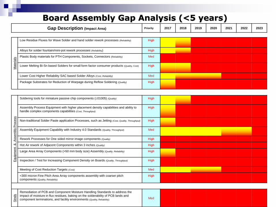
Gap Description (Impact Area) Priority 2017 2018 2019 2020 2021 2022 2023
Mate
ria
ls
Low Residue Fluxes for Wave Solder and hand solder rework processes (Reliability) High
Alloys for solder fountain/mini-pot rework processes (Reliability) High
Plastic Body materials for PTH Components, Sockets, Connectors (Reliability) Med
Lower Melting Bi-Sn based Solders for small form factor consumer products (Quality, Cost) High
Lower Cost Higher Reliability SAC based Solder Alloys (Cost, Reliability) Med
Package Substrates for Reduction of Warpage during Reflow Soldering (Quality) High
Equip
ment
&
Assem
bly
Pro
cess
Soldering tools for miniature passive chip components (01005) (Quality) High
Assembly Process Equipment with higher placement density capabilities and ability to
handle complex components capabilities (Cost, Throughput)
High
Non-traditional Solder Paste application Processes, such as Jetting (Cost, Quality, Throughput) High
Assembly Equipment Capability with Industry 4.0 Standards (Quality, Throughput) Med
Rework Processes for One sided mirror image components (Quality) High
Hot Air rework of Adjacent Components within 3 inches (Quality) High
Large Area Array Components (>50 mm body size) Assembly (Quality, Reliability) High
Inspection / Test for Increasing Component Density on Boards (Quality, Throughput) High
Meeting of Cost Reduction Targets (Cost) Med
<300 micron Fine Pitch Area Array components assembly with coarser pitch
components (Quality, Reliability)
High
Stn
ds
Remediation of PCB and Component Moisture Handling Standards to address the
impact of moisture in flux residues, baking on the solderability of PCB lands and
component terminations, and facility environments (Quality, Reliability)Med
Board Assembly Gap Analysis (<5 years)

2017 Roadmap
Optoelectronic
TWG Chapter
Highlights
58
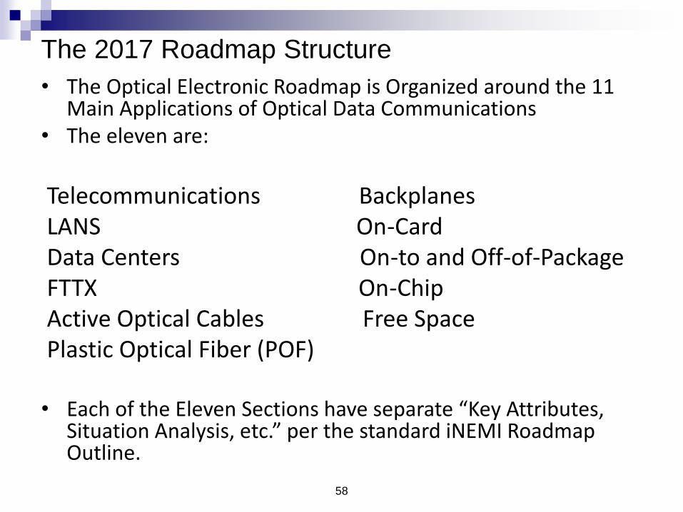
The 2017 Roadmap Structure
• The Optical Electronic Roadmap is Organized around the 11 Main Applications of Optical Data Communications
• The eleven are:
Telecommunications BackplanesLANS On-CardData Centers On-to and Off-of-PackageFTTX On-ChipActive Optical Cables Free Space Plastic Optical Fiber (POF)
• Each of the Eleven Sections have separate “Key Attributes, Situation Analysis, etc.” per the standard iNEMI Roadmap Outline.
59
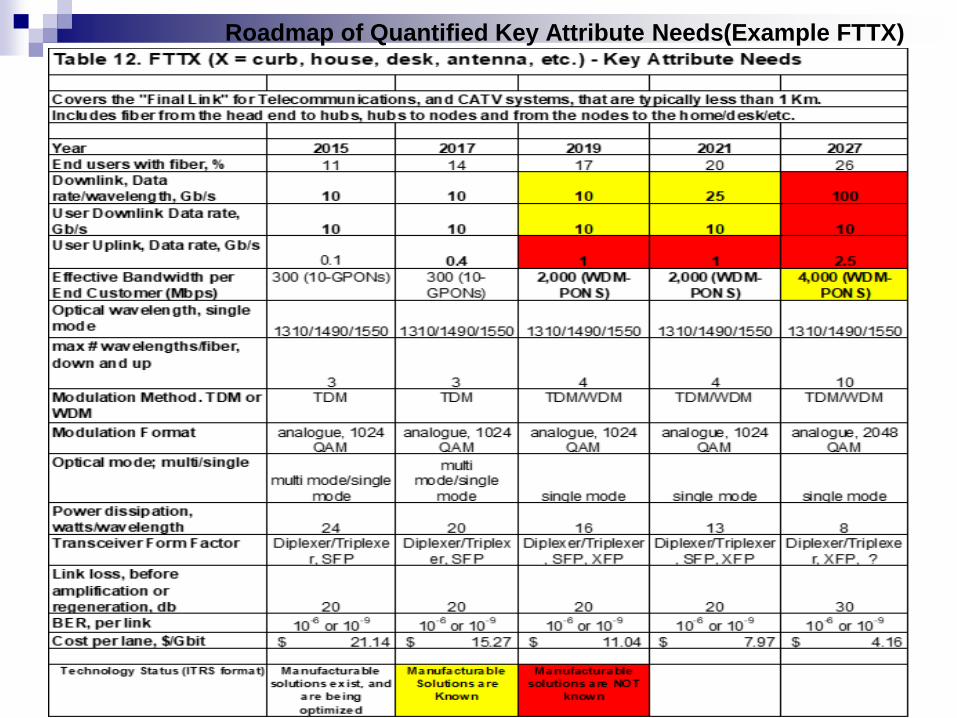
Roadmap of Quantified Key Attribute Needs(Example FTTX)
Market and Application Mapping
Application areas
Table 2: Optical Data Communications Application, Group #1
iNEMI PEG (Market Segment)
Telecom FTTX LANs Data Centers
Plastic Optical Fiber (POF)
AOC
Consumer/Office Systems
Products Stable
Major Application
Product Growth
Major User
Minor Application
Application Growing
High End Systems N/A N/A Major
Application Supportin
g Data Centers
N/A Major Application
Medical Some
Application N/A Application
Stable Growing
User N/A Minor
Application
Automotive
N/A N/A Demo’s R&D
Minimal user in 2016;
potentially Key to
self-driving cars
Major Application
Much Potential
Application
Portable/Wireless
Products Stable
Application Growing
Application Growing
Driver of need for Data Centers
Minor Application
Minor Application
Aerospace/Defense Products
Stable N/A Products
Stable Minimal
Use Ground & Air Vehicle
Application Growing
IoT & Wearables Applications
Emerging Applications
Emerging Minimal
Application Minimal Impact
Some Application
Minimal Application
Market and Application Mapping (2)
Application areas
Table 2: Optical Data Communications, Group #2
iNEMI PEG (Market Segment)
Backplane On-card In-to and Out-of Package
On-chip Free Space
Consumer/Office Systems
R&D R&D R&D Concept User
High End Systems R&D R&D R&D Concept NA
Medical N/A Limited
Application Limited
Application N/A Potential
User
Automotive N/A N/A N/A N/A NA
Portable/Wireless Some
Application Product R&D Product R&D Product
R&D Potential
User
Aerospace/Defense
Product R&D Some Application
Concept Concept User
IoT & Wearables
NA NA Some Application
Potential Sensor Related
Application
Some Application
Optoelectronic Substrate Issues
Laminated and embedded wave guides are likely to be enabling technologies for
high speed optical backplane and chip-to-chip applications.
Outsourcing of manufacturing by OEMs to CMs and EMS companies, leads to
wider dissemination of previously closely held package, assembly process and test
knowledge. There is a growing realization that most of the intellectual property (IP)
is in the design and functional performance.
A major impediment to acceptance of lower cost “datacom” components by
network service providers is the requirement for rigorous reliability and testing to
“telecom” standards, such as Telcordia GR1221
Detailed Roadmap needs for photonics is being refined by the iNEMI led
International Photonics Systems Roadmap (IPSR)
Key pre-competitive collaboration priorities were published on June 30, 2016.
62
63
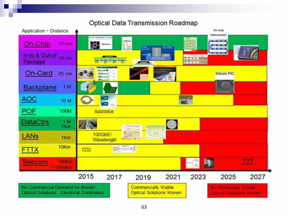
Optical Data Transmission Situation Summary
The growing demand for greater data transmission capacity, smaller
physical size and lower power consumption increasingly favors
optical methods and results in optical technologies replacing copper
as soon as the total cost of the optical solution is competitive.
With the cost of power rising, and data transmission rates
increasing, optical technologies will continue to replace copper at
shorter distances.
The current crossover where optical methods are better than copper
is a distance of 1 to 10-meters when data rates are 10 to 100 Gb/s.
The historic major market has been metro and long haul
telecommunications but that market is now being surpassed by the
demand for optics in Data Centers.
The major reasons for adopting optical data transmission are:
Its ability to transfer data at 10 to 100 Gb/s rates.
The relatively small amount of power
The ~75% smaller size of optical cables vs copper cables in high (10Gb/s+) data
rate applications.
The Optical Data Communication Situation Summary (Continued): Use in Long Haul and Metropolitan Communications continues with 100 Gb/s capability growing in importance.
Ethernet is moving to 100 Gb/s data rates implemented with 4 x 25Gb/s methods.
400 Gb/s Ethernet using 4 x 100 Gb/s under discussion.
Data Centers are major consumers and drivers of optical technology, especially AOCs (Active Optical Cables) to implement
Ethernet and Fiber Channel links.
FTTX, including CATV that utilizes hybrid fiber coax technology, is an important high speed data link to the consumer for the
“last mile”.
FTTX is growing as fiber is taken closer to the end user to provide high data rate connectivity to the internet.
Backplanes
Copper is OK to 20+ Gb/s - up to 1 meter.
No widely adopted approach to utilizing optics in backplanes has emerged although the introduction of daughter card to
backplane optical connectors utilizing the expanded beam concept is promising.
A major barrier to adoption is the high risk of re-engineering backplanes to incorporate optical transmission media.
On-card data transfer
Use is beginning with much interest and several applications announced.
Much technology has been demonstrated but cost is questionable unless data rates are > 10 Gb/s and the application
demands optical methods.
In-to and Out-of Package
Optical methods offer a potential solution for the 10Tb/s+ IO data rates forecast by the ITRS for multicore processors in
2017.
Optical methods offer lower power and more bandwidth in less area.
On-chip
Exploring for lower power and more bandwidth.
A modulated light source is needed.
Application not expected for 10+ years.
Free Space
Interest for local data transmission within a room is developing due to the greater security resulting from the elimination of
RF.
Communication through space where the security of a tight communication beam is important.
66
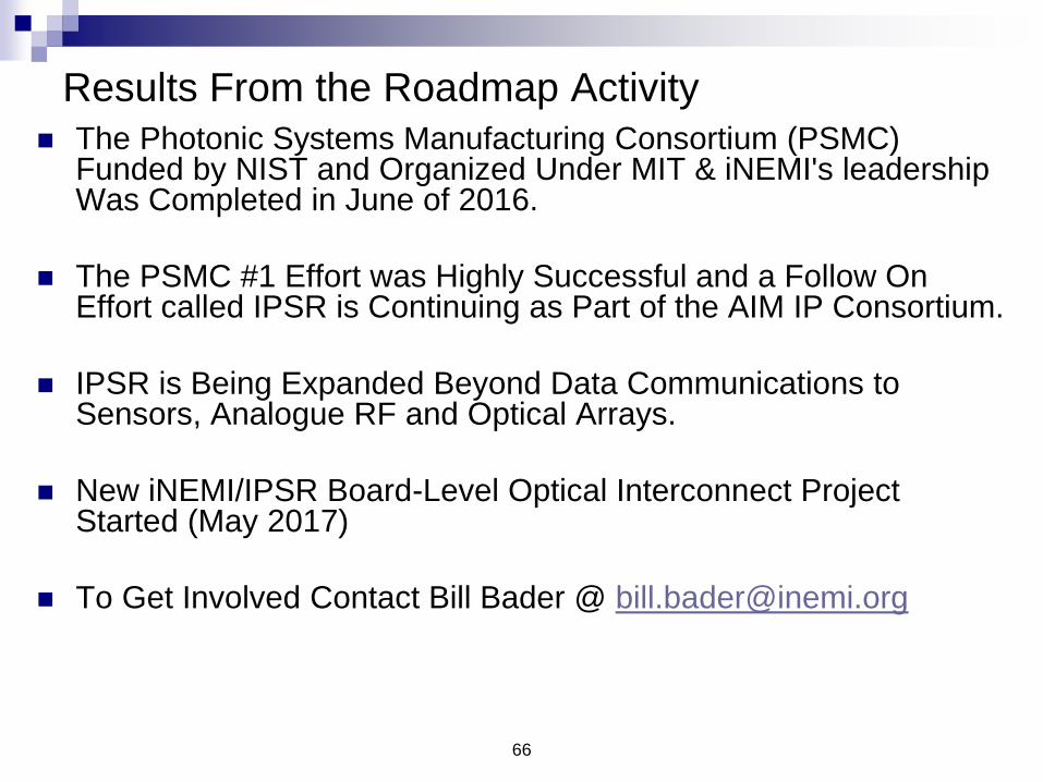
Results From the Roadmap Activity
The Photonic Systems Manufacturing Consortium (PSMC) Funded by NIST and Organized Under MIT & iNEMI's leadership Was Completed in June of 2016.
The PSMC #1 Effort was Highly Successful and a Follow On Effort called IPSR is Continuing as Part of the AIM IP Consortium.
IPSR is Being Expanded Beyond Data Communications to Sensors, Analogue RF and Optical Arrays.
New iNEMI/IPSR Board-Level Optical Interconnect Project Started (May 2017)
To Get Involved Contact Bill Bader @ [email protected]

From the Roadmap comes
collaborative Projects. Example:
Board Level Optical Interconnects
Project , IPSR
Tom Marrapode
Background
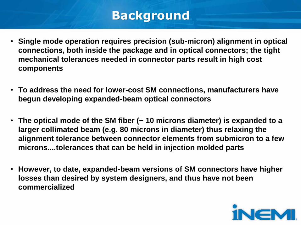
• Single mode operation requires precision (sub-micron) alignment in optical
connections, both inside the package and in optical connectors; the tight
mechanical tolerances needed in connector parts result in high cost
components
• To address the need for lower-cost SM connections, manufacturers have
begun developing expanded-beam optical connectors
• The optical mode of the SM fiber (~ 10 microns diameter) is expanded to a
larger collimated beam (e.g. 80 microns in diameter) thus relaxing the
alignment tolerance between connector elements from submicron to a few
microns....tolerances that can be held in injection molded parts
• However, to date, expanded-beam versions of SM connectors have higher
losses than desired by system designers, and thus have not been
commercialized
Background
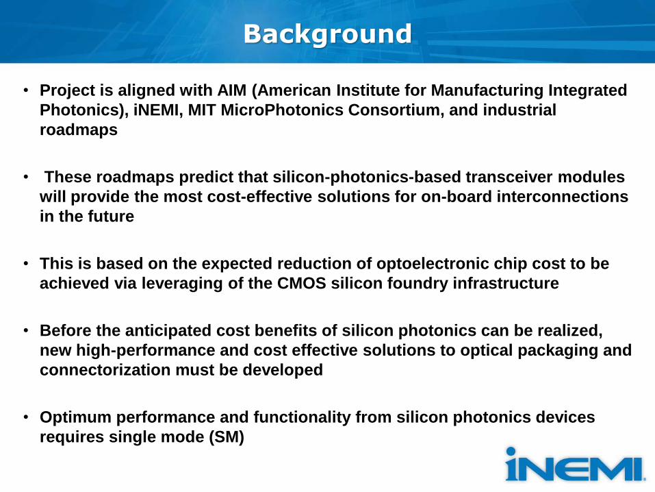
• Project is aligned with AIM (American Institute for Manufacturing Integrated
Photonics), iNEMI, MIT MicroPhotonics Consortium, and industrial
roadmaps
• These roadmaps predict that silicon-photonics-based transceiver modules
will provide the most cost-effective solutions for on-board interconnections
in the future
• This is based on the expected reduction of optoelectronic chip cost to be
achieved via leveraging of the CMOS silicon foundry infrastructure
• Before the anticipated cost benefits of silicon photonics can be realized,
new high-performance and cost effective solutions to optical packaging and
connectorization must be developed
• Optimum performance and functionality from silicon photonics devices
requires single mode (SM)
Project Purpose
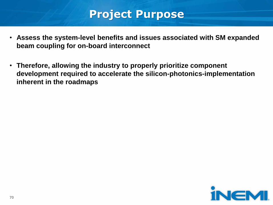
• Assess the system-level benefits and issues associated with SM expanded
beam coupling for on-board interconnect
• Therefore, allowing the industry to properly prioritize component
development required to accelerate the silicon-photonics-implementation
inherent in the roadmaps
70
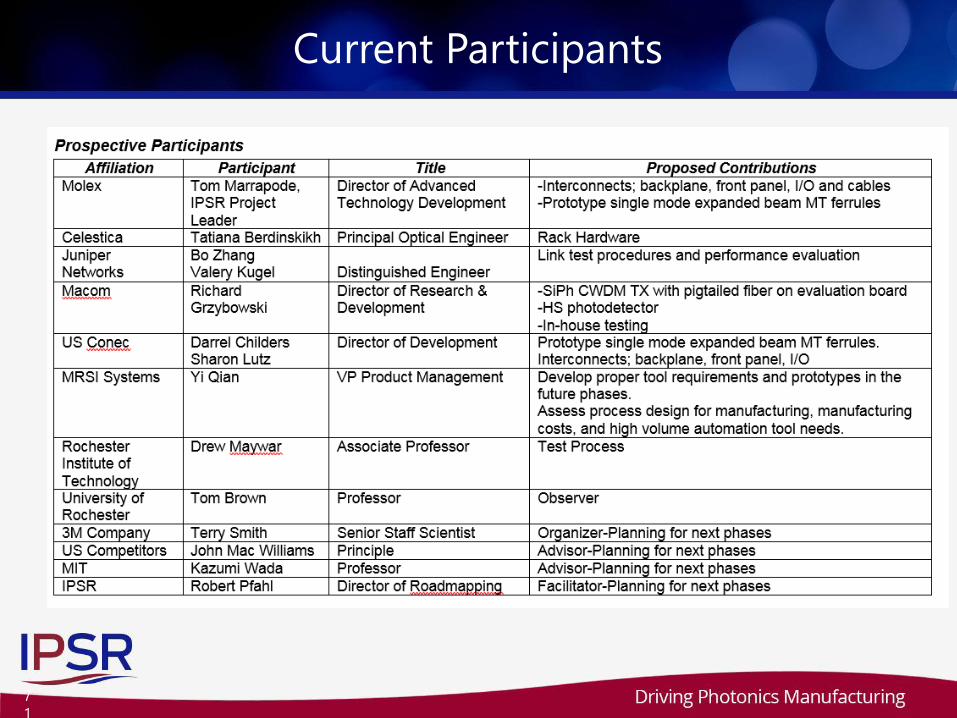
Current Participants
7
1
72
Product
Needs
Technology
Evolution
Gap
Analysis/
Technical
Plan
Research
Projects
Implementation
Competitive
Solutions
RoadmapProject
Completion
Industry Solution
Needed
Academia
Government
iNEMI
Users & Suppliers
Regional
Collaboration
No Work
Required or
Outsourced
Available
to Market
Place
Global
Participation
Disruptive
Technology
Roadmap Next Steps: Identify Initiatives to Close Gaps

iNEMI
Collaborative Project
Activities
74
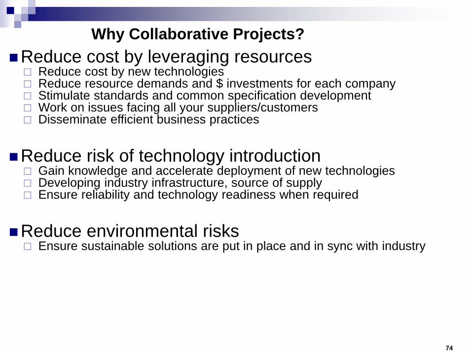
Reduce cost by leveraging resources Reduce cost by new technologies Reduce resource demands and $ investments for each company Stimulate standards and common specification development Work on issues facing all your suppliers/customers Disseminate efficient business practices
Reduce risk of technology introduction Gain knowledge and accelerate deployment of new technologies Developing industry infrastructure, source of supply Ensure reliability and technology readiness when required
Reduce environmental risks Ensure sustainable solutions are put in place and in sync with industry
Why Collaborative Projects?
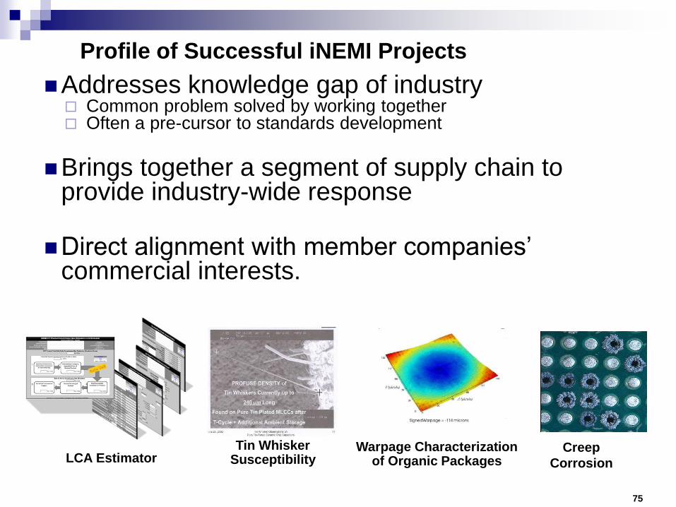
Profile of Successful iNEMI Projects
75
Addresses knowledge gap of industry Common problem solved by working together Often a pre-cursor to standards development
Brings together a segment of supply chain to provide industry-wide response
Direct alignment with member companies’ commercial interests.
Warpage Characterization of Organic PackagesLCA Estimator
Creep
Corrosion
Tin Whisker Susceptibility
12 Ongoing Projects July - August 2017
76
Project Name TIG Est Start
Date
Est End
Date
BiSn Based Low Temperature Soldering Process and
Reliability
Board Assembly 2/1/2016 10/31/2017
Characterization of Pb-Free Alloy Alternatives Project Board Assembly 11/17/2015 6/30/2017
Characterize and quantify the inspection capability of the
AXI on HoP HiP defects
Test & Inspection 7/28/2016 1/31/2018
Connector Reliability Test Recommendations Project,
Phase 2
Board Assembly 3/1/2017 3/29/2019
Development of Cleanliness Specification for Expanded
Beam Connectors Project, Phase II
Optoelectronic 3/1/2017 3/2/2018
Final Assembly Automation and Optimization Other 9/6/2016 12/1/2017
Impact of Low CTE Mold Compound on Second Level
Board Reliability Phase 2
Board Assembly 3/31/2016 2/28/2018
IPSR - Board-Level Optical Interconnect Project Optoelectronic 5/5/2017 5/31/2018
QFN Package Board Level Reliability Project Board Assembly 8/5/2015 12/29/2017
Qualification Test Development for Creep Corrosion, Phase
3
Board Assembly 2/1/2016 8/4/2017
Reuse and Recycling Metrics - Phase 2 Sustainable
Electronics
4/6/2017 2/28/2019
SiP Module Mold-ability Study Packaging 6/10/2016 12/1/2017
Active Initiatives
77
Initiative Project Name Status TIG Chair Name Member -
Company
Initiative -
Start Date
PCB Warpage Characterization and Minimization
Project
TC Approval/In
Sign-up
Board
Assembly
Srini
Aravamudhan
Intel 3/15/2017
Warpage Characteristics of Organic Packages
Phase 4
TC Approval/In
Sign-up
Board
Assembly
Wei Keat Loh Intel 4/4/2017
Wafer and Panel Level Package: Warpage and
Flowability
In-Progress Board
Assembly
Renn Chan Ooi Intel 5/4/2017
Solder Joint Fracture as a Function of Warpage Consideration Board
Assembly
Ron Kulterman Flextronics 4/1/2017
Value Recovery from Use Electronics Phase 2 TC Approval/In
Sign-up
Sustainable
Electronics
Bill Olson Seagate 9/15/2017
Eco-Design Best Practices TC Approval/In
Sign-up
Sustainable
Electronics
Pamela Gordon Antea
Group
4/7/2017
Methodology for Qualifying New Packaging
Technology
TC Approval/In
Sign-up
Packaging Feng Feng Xue IBM 3/21/2017
Fine Pitch Circuit Pattern Inspection/Metrology
Project Plase2
In-Progress Packaging Feng Feng Xue IBM 3/7/2017
High Temperature, Pb-free Die Attach Material
Phase 2
Consideration Packaging Sze Pei Lim Indium 4/6/2017
Initiative Example
Approaches to minimize Printed Circuit Board (PCB) warpage in Board Assembly Process to improve SMT Yield
Call for Project Sign UpSeptember 2017
Initiative Leaders: Srini Aravamudhan & Chris Combs, Intel;iNEMI Staff: Haley Fu
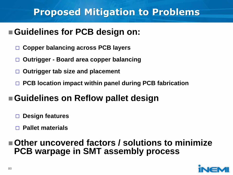
Proposed Mitigation to Problems
Guidelines for PCB design on:
Copper balancing across PCB layers
Outrigger - Board area copper balancing
Outrigger tab size and placement
PCB location impact within panel during PCB fabrication
Guidelines on Reflow pallet design
Design features
Pallet materials
Other uncovered factors / solutions to minimize PCB warpage in SMT assembly process
80
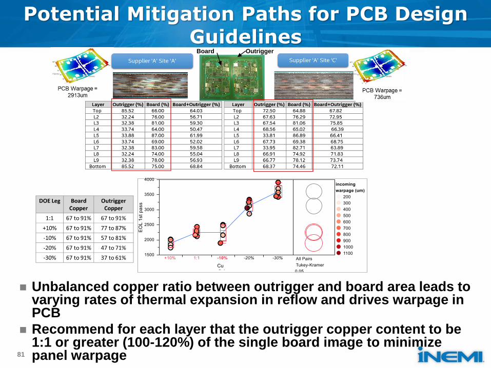
Potential Mitigation Paths for PCB Design Guidelines
Unbalanced copper ratio between outrigger and board area leads to varying rates of thermal expansion in reflow and drives warpage in PCB
Recommend for each layer that the outrigger copper content to be 1:1 or greater (100-120%) of the single board image to minimize panel warpage81
OutriggerBoard
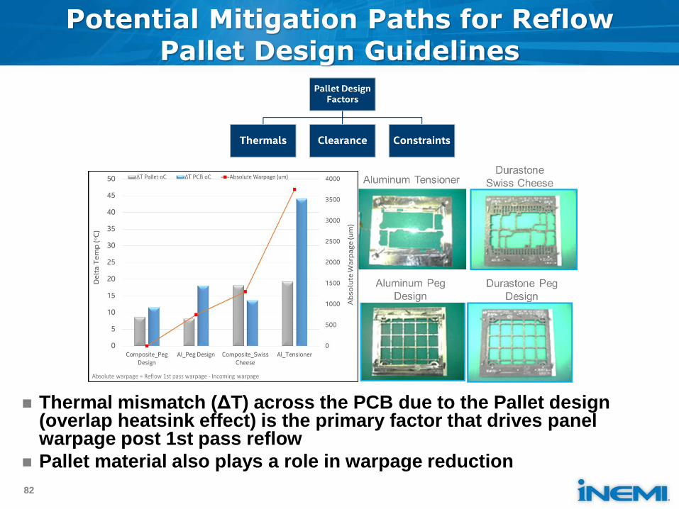
Potential Mitigation Paths for Reflow Pallet Design Guidelines
82
Thermal mismatch (ΔT) across the PCB due to the Pallet design (overlap heatsink effect) is the primary factor that drives panel warpage post 1st pass reflow
Pallet material also plays a role in warpage reduction
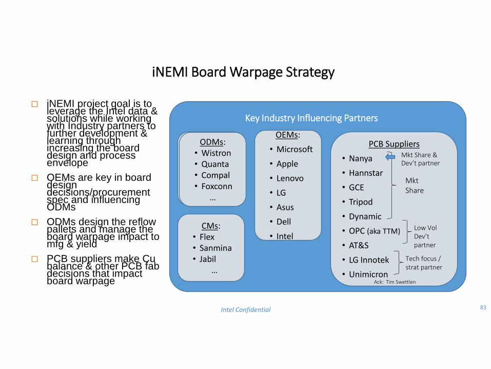
iNEMI Board Warpage Strategy
iNEMI project goal is to leverage the Intel data & solutions while working with Industry partners to further development & learning through increasing the board design and process envelope
OEMs are key in board design decisions/procurement spec and influencing ODMs
ODMs design the reflow pallets and manage the board warpage impact to mfg & yield
PCB suppliers make Cu balance & other PCB fab decisions that impact board warpage
83Intel Confidential
PCB Suppliers
• Nanya
• Hannstar
• GCE
• Tripod
• Dynamic
• OPC (aka TTM)
• AT&S
• LG Innotek
• Unimicron
CMs: • Flex• Sanmina• Jabil
…
ODMs:• Wistron• Quanta• Compal• Foxconn
…
Mkt Share
Mkt Share & Dev’t partner
Low Vol Dev’t partner
Tech focus / strat partner
OEMs:
• Microsoft
• Apple
• Lenovo
• LG
• Asus
• Dell
• Intel
Key Industry Influencing Partners
Ack: Tim Swettlen
ODMs:• Wistron• Quanta• Compal• Foxconn
…
Completing the 2017 iNEMI Roadmap/Starting the 2019
Cycle
2017 iNEMI Roadmap Development Cycle is wrapped up!
2017 iNEMI Technology Plan Planned for Publication End of September
2017 iNEMI Research Priorities Document expected to be published
end of October 2017 & Available Free at www.inemi.org
2017 Roadmap Available Free to iNEMI Member Companies
Available To Industry:
Order the 2017 iNEMI Roadmap via download at www.inemi.org
Individual roadmap chapters are also available as a PDF document download at
www.inemi.org
2019 iNEMI Roadmap is being developed now for publication to
members in late December, 2018 and the industry in late March,
2019 so take advantage of the opportunity to participate (iNEMI
Membership not required for roadmap participation).
Contact Chuck Richardson for more details at [email protected]