241-208 ch71 chapter 5 sequential circuits: flip-flops and counter by taweesak reungpeerakul
TRANSCRIPT

241-208 CH7 1
Chapter 5
Sequential Circuits: Flip-Flops and Counter
By Taweesak Reungpeerakul

241-208 CH7 2
Contents Introduction Latches Edge-Triggered Flip-Flops (ET-FFs) Operating Characteristics and Application Asynchronous Counter Synchronous Counter Cascaded Counters Counter Decoding Counter Applications
Conclusions

241-208 CH7 3
Contents Basic Shift Register Functions Serial In/Serial Out Shift Registers Serial In/Parallel Out Shift Registers Parallel In/Serial Out Shift Registers Parallel Out/Parallel Out Shift Registers Bidirectional Shift Registers Shift Register Counters Shift Register Applications Conclusions

241-208 CH7 4
Introduction
Well, what u learned before is just one class of digital circuits.
In fact we can classify into two main classes :-
Output can depend on the past and present inputs/outputs.
Output depends on the present input.

241-208 CH7 5
Introduction (cont.)
Synchronous VS Asynchronous
•All state transitions are controlled by a common clock
•Changes in all variables occurconcurrently
•State transitions occur independently of any clock
•Changes in all variables do not necessarily occur concurrently

241-208 CH7 6
RQ
QS
Latches
A latch is a temporary storage device that has two stable states (bistable). It is a basic form of memory.
The S-R (Set-Reset) latch is the most basic type. It can be constructed from NOR gates or NAND gates.
R
S
Q
Q
NOR Active-HIGH Latch NAND Active-LOW Latch

241-208 CH7 7
The active-HIGH S-R latch is in a stable (latched) condition when both inputs are LOW. R
S
Q
Q
Assume the latch is initially RESET (Q = 0) and the inputs are at their inactive level (0). To SET the latch (Q = 1), a momentary HIGH signal is applied to the S input while the R remains LOW.
0 1
0
R
S
Q
Q
1
0
0
To RESET the latch (Q = 0), a momentary HIGH signal is applied to the R input while the S remains LOW. 0
0
1
01
0
Latch initially RESET
Latch initially SET
S-R Latch

241-208 CH7 8
S
R
The active-LOW S-R latch is in a stable (latched) condition when both inputs are HIGH.
Q
Q
1 1
01
0
1
Latch initially RESET
Q
Q
1
1
01
01
Latch initially SET
S
R
Assume the latch is initially RESET (Q = 0) and the inputs are at their inactive level (1). To SET the latch (Q = 1), a momentary LOW signal is applied to the S input while the R remains HIGH.
To RESET the latch a momentary LOW is applied to the R input while S is HIGH.Never apply an active set and reset at the same time (invalid).
S-R Latch (cont.)

241-208 CH7 9
A gated latch is a variation on the basic latch.The gated latch has an additional input, called enable (EN) that must be HIGH in order for the latch to respond to the S and R inputs.
R
SQ
Q
EN
Show the Q output with relation to the input signals. Assume Q starts LOW.Keep in mind that S and R are only active when EN is HIGH.
S
R
ENQ
Latch with Enable

241-208 CH7 10
The D latch is an variation of the S-R latch but combines the S and R inputs into a single D input as shown:
A simple rule for the D latch is: Q follows D when the Enable is active.
D
EN
Q
QD
EN
D Latch

241-208 CH7 11
The truth table for the D latch summarizes its operation. If EN is LOW, then there is no change in the output and it is latched.
Inputs
Comments
01X
END
110
Outputs
01Q0
10
Q0
RESETSETNo change
Truth Table of D Latch

241-208 CH7 12
Determine the Q output for the D latch, given the inputs shown.
EN
Q
D
Notice that the Enable is not active during these times, so the output is latched.
Q
QD
ENExample

241-208 CH7 13
Edge-Triggered Flip-Flops
Circuit type: Synchronous bistable deviceQ:What is bistable ?A: Remain in one of two stable states until it receives a pulse (logic 1 signal) through one of its inputs, upon which it switches, or ‘flips’, over to the other state.

241-208 CH7 14
Edge-Triggered Flip-Flops (cont.)
ET-FF characteristics:•1-bit storage devices
Why? 1) Since outputs can be set to store either ‘0’ or ‘1’, depending on the inputs
2) outputs retain their prescribed values (bistable prop.)
•FF have 2 complimentary outputs (Q, Q)•Three main FF types: R-S, D-type, J-K
•Changes state either at the positive or negative edge of the clock pulse

241-208 CH7 15
Edge-Triggered Flip-Flops (cont.)
D Q
C
Q
(a) Positive edge-triggered
D Q
C
Q
(b) Negative edge-triggered
Dynamic input indicator
The active edge can be positive or negative.
Inputs
Comments
1
CLKD
Outputs
1
0 SET0 0 1 RESET
Inputs
Comments
1
CLKD
Outputs
1
0 SET0 0 1 RESET

241-208 CH7 16
Edge-Triggered Flip-Flops (cont.)
CLK
K
J
Q
Q
Positive ET-J-K FF symbol
1. More versatile than other FFs.2. Has 2 inputs (J and K) and 2 outputs

241-208 CH7
Edge-Triggered Flip-Flops (cont.)

241-208 CH7 18
Edge-Triggered Flip-Flops (cont.)
Inputs
Comments
1
1 1
1
CLKKJ
Outputs
1
Q0
Q0
Q0
Q0
0 SETToggle
0
0
00 0 1 RESET
No change
Positive ET-J-K FF truth table
How comes ?
CLK
K
J
Q
Q
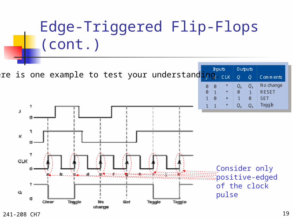
241-208 CH7 19
Edge-Triggered Flip-Flops (cont.)
Inputs
Comments
1
1 1
1
CLKKJ
Outputs
1
Q0
Q0
Q0
Q0
0 SETToggle
0
0
00 0 1 RESET
No change
Consider only positive-edged of the clock pulse
Here is one example to test your understanding.

241-208 CH7 20
Edge-Triggered Flip-Flops (cont.)
Inputs
Comments
1
1 1
1
CLKKJ
Outputs
1
Q0
Q0
Q0
Q0
0 SETToggle
0
0
00 0 1 RESET
No changeOne more example and try to figure out by yourself !!
CLK
Q
K
J
Set
Toggle Set
Latch

241-208 CH7 21
Edge-Triggered Flip-Flops (cont.)
Asynchronous Preset and Clear inputs
FF outputs are independent of the clock if either “Preset” or “Clear” is asserted.
CLK
K
J
Q
Q
PRE
CLR

241-208 CH7 22
Edge-Triggered Flip-Flops (cont.)
Set Toggle Reset Toggle
Set
Set
Reset
Latch
CLK
K
J
Q
PRE
CLR
Check by yourself for this example !
CLK
K
J
Q
Q
PRE
CLR

241-208 CH7 23
FFs Operating CharacteristicsPropagation delay time is specified for the rising and falling outputs. It is measured between the 50% level of the clock to the 50% level of the output transition.
50% point on triggering edge
50% point
50% point on LOW-to-HIGH transition of Q
tPLH tPHL
CLK CLK
Q Q 50% point on HIGH-to- LOW transition of Q
The typical propagation delay time for the 74AHC family (CMOS) is 4 ns. Even faster logic is available for specialized applications.

241-208 CH7 24
FFs Operating Characteristics (cont.)
Another propagation delay time specification is the time required for an asynchronous input to cause a change in the output. Again it is measured from the 50% levels. The 74AHC family has specified delay times under 5 ns.
50% point
tPLHtPHL
Q 50% point50% point
50% point
Q
PRE CLR
241-208 CH7 25
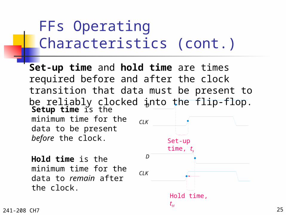
FFs Operating Characteristics (cont.)
Set-up time and hold time are times required before and after the clock transition that data must be present to be reliably clocked into the flip-flop.Setup time is the minimum time for the data to be present before the clock.
Hold time is the minimum time for the data to remain after the clock.
CLK
D
CLK
D
Set-up time, ts
Hold time, tH

241-208 CH7 26
FFs Operating Characteristics (cont.)
Some other important characteristics are:-
•Maximum clock frequency
•Pulse widths
•Power dissipation
•Speed-power product

241-208 CH7 27
FF Applications
•Parallel data storage
•Frequency division
•Counter (will be illustrated in detail later on)
241-208 CH7 28
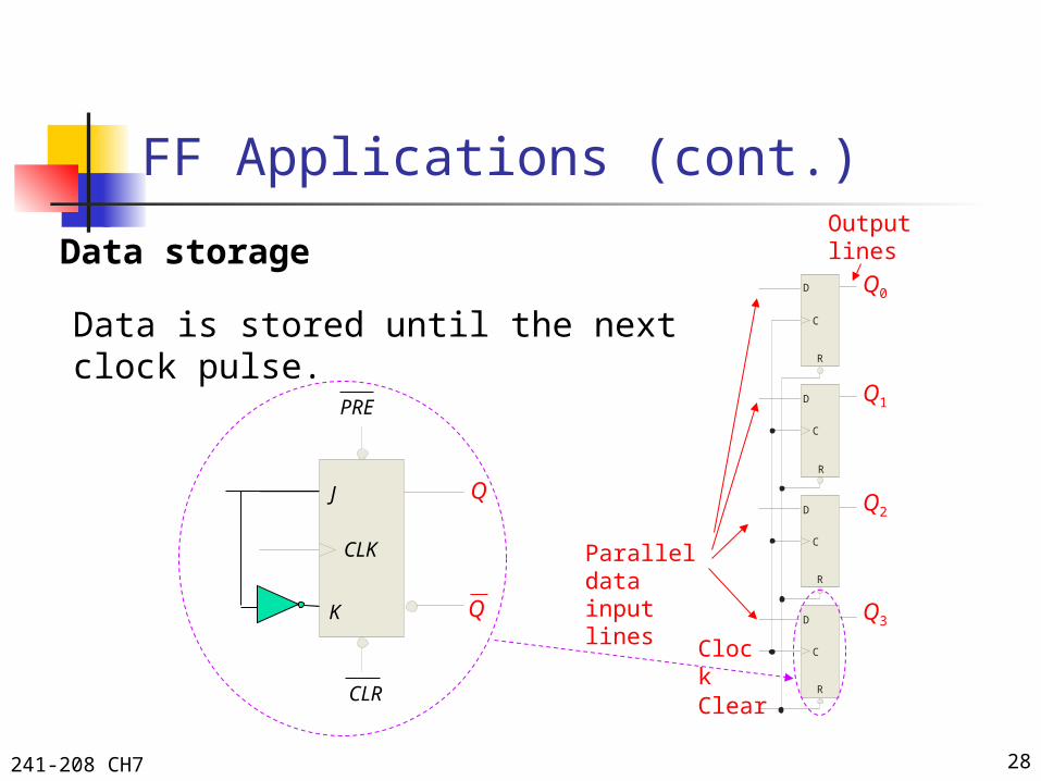
FF Applications (cont.)
D
C
R
D
C
R
D
C
R
D
C
R
Parallel data input lines
Clock
Clear
Output lines
Q0
Q1
Q2
Q3
Data storage
Data is stored until the next clock pulse.
CLK
K
J
Q
PRE
CLR
Q

241-208 CH7 29
FF Applications (cont.)For frequency division, it is simple to use a flip-flop in the toggle mode or to chain a series of toggle flip flops to continue to divide by two.
One flip-flop will divide fin by 2, two flip-flops will divide fin by 4 (and so on). A side benefit of frequency division is that the output has an exact 50% duty cycle.
HIGH HIGH
CLK
K
JQA
CLK
K
J
fin
QB fout
Waveforms:fin
fout

241-208 CH8 30
Counter
Counting in binary.
LSB changes on every number.
The next bit changes on every other number.
0 0 00 0 10 1 00 1 11 0 01 0 11 1 01 1 1
The next bit changes on every fourth number.

241-208 CH8 31
Counter (cont.)
Counter can be formed by connecting FFs together
Counter can be categorized into two cases, according to the ways they are clocked !!
•Asynchronous counter (ripple counter)
Each FF formed counter do not change their states at the same time
•Synchronous counter
Each FF in this counter is clocked concurrently.

241-208 CH8 32
Asynchronous Counters
In an asynchronous counter, the clock is applied only to the first stage. Subsequent stages derive the clock from the previous stage.
Three bit asynchronous counter
The three-bit asynchronous counter shown is typical. It uses J-K flip-flops in the toggle mode.
CLK
K0
J0
Q0
Q0
C C C
J1 J2
K1 K2
Q1 Q2
Q1
HIGH
Waveforms are on the following slide…

241-208 CH8 33
Asynchronous Counters (cont.)
CLK
Q0
Q1
Q2
1 2 3 4 5 6 7 8
10 10 10 10 0
10 10 01010
00 11 01100
Notice that the Q0 output is triggered on the leading edge of the clock signal. The following stage is triggered from Q0. The leading edge of Q0 is equivalent to the trailing edge of Q0. The resulting sequence is that of an 3-bit binary up counter.

241-208 CH8 34
Asynchronous Counters (cont.)
Propagation delayAsynchronous counters are sometimes called ripple counters, because the stages do not all change together. For certain applications requiring high clock rates, this is a major disadvantage.
Notice how delays are cumulative as each stage in a counter is clocked later than the previous stage.
CLK
Q0
Q1
Q2
1 2 3 4
Q0 is delayed by 1 propagation delay, Q2 by 2 delays and Q3 by 3 delays.

241-208 CH8 35
Asynchronous Counters (cont.)The modulus of a counter is the number of output states it goes through before returning its self back to zero.
The maximum possible number of states (maximum modulus) of a counter is 2n
CLK
K0
J0
Q0
Q0
C C C
J1 J2
K1 K2
Q1 Q2
Q1
HIGH
Counter with 3 FFs count from 0-7 and called modulo-8 counter.
Counters can be designed to have a number of states in their sequences <2n
. This type of sequence is called a
truncated sequence.

241-208 CH8 36
Asynchronous Counters (cont.)Asynchronous decade counter
This counter uses partial decoding to recycle the count sequence to zero after the 1001 state (modulo-10 counter).
CLK
K0
J0
Q0
C C C
J1 J2
K1 K2
Q1 Q2
HIGH
C
J3
K3
Q3
CLR
Use the output of NAND gateto clear input of the FFs

241-208 CH8 37
Asynchronous Counters (cont.)
Asynchronous decade counter (cont.)
When Q1 and Q3 are HIGH together, the counter is cleared by a “glitch” on the CLR line.
1 2 3 4 5 6 7 8 9 10
Glitch
Glitch
CLK
Q0
Q1
Q2
Q3
CLR
Glitch
Glitch

241-208 CH8 38
Asynchronous Counters (cont.)The 74LS93A asynchronous counter
(9)(12) (8) (11)
(1)
(14)
(2)
(3)
The 74LS93A has one independent toggle J-K flip-flop driven by CLK A and three toggle J-K flip-flops that form an asynchronous counter driven by CLK B.
CLK A
K0
J
0
Q0
C C C
J
1
J
2
K1 K2
Q1 Q2
C
J
3
K3
Q3
CLK B
The counter can be extended to form a 4-bit counter by connecting Q0 to the CLK B input. Two inputs are provided that clear the count.
RO (1)
RO (2)All J and K inputs are connected internally HIGH

241-208 CH8 39
J
Q
Q
K
SET
CLR
J
Q
Q
K
SET
CLR
HIGH
CLK
Q0 Q1
Q1
FF0 FF1
Synchronous Counters
CLK
Q0
Q1
Propagation delay through FF0
CLK
Q0
Q1
Propagation delay through FF0
Propagation delay through FF1
All flip-flops are clocked together with a common clock pulse.
Trade small propagation delays with more circuitry to control states changes.Toggle mode
CLK
Q0
Q1
Propagation delay through FF0
CLK
Q0
Q1
Propagation delay through FF0
Propagation delay through FF1

241-208 CH8 40
Synchronous Counters (cont.)
CLK
Q0
Q1
1 2 3 4
Timing diagram of 2-bit synchronous counter
J
Q
Q
K
SET
CLR
J
Q
Q
K
SET
CLR
HIGH
CLK
Q0 Q1
Q1
FF0 FF1
241-208 CH8 41
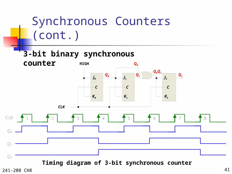
Synchronous Counters (cont.)
K0
J
0
Q0
C C C
J
1
J
2
K1 K2
Q0Q1Q0 Q1 Q2
CLK
HIGH
3-bit binary synchronous counter
CLK
Q0
Q1
1 2 3 4 5 6 7 8
Q2
Timing diagram of 3-bit synchronous counter

241-208 CH8 42
Synchronous Counters (cont.)Analysis of synchronous counters (Tabular technique)
Q2 Q1 Q0 J2 = Q0Q1 K2 = Q0Q1 J1 = Q0 K1 = Q0 J0 = 1 K0 = 1
Outputs Logic for inputs
1. Put the counter in an arbitrary state; then determine the inputs for this state.
0 0 0 0 0 0 0 1 1
2. Use the new inputs to determine the next state: Q2 and Q1 will latch and Q0 will toggle.
0 0 1 0 0 1 1 1 1
3. Set up the next group of inputs from the current output.
0 1 0 4. Q2 will latch again but both Q1 and Q0 will toggle.
K0
J
0
Q0
C C C
J
1
J
2
K1 K2
Q0Q1Q0 Q1
Q2
CLK
HIGH

241-208 CH8 43
Synchronous Counters (cont.)Analysis of synchronous counters (Tabular technique)
Outputs Logic for inputs
0 0 0 0 0 0 0 1 1
0 0 1 0 0 1 1 1 1
0 1 0
Q2 Q1 Q0 J2 = Q0Q1 K2 = Q0Q1 J1 = Q0 K1 = Q0 J0 = 1 K0 = 1
1 1
1 1
1 1
1 1
1 1
1 1
0 1 1
1 0 0
1 0 1
1 1 0
1 1 1
0 0 0
0 0 0 0
1 1 1 1
0 0 0 0
0 0 1 1
0 0 0 0
1 1 1 1
At this points all states have been accounted for and the counter is ready to recycle…
241-208 CH8 44
Synchronous Counters (cont.)
J0 Q0
C
K0 Q0
HIGH
CLK
FF0
J1 Q1
C
K1 Q1
FF1
J2 Q2
C
K2 Q2
FF2
J3 Q3
C
K3 Q3
FF3
Q1Q0Q2Q1Q0G1
G2
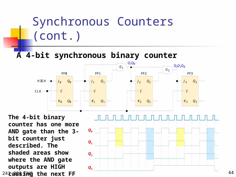
A 4-bit synchronous binary counter
Q0
Q1
Q2
Q3
The 4-bit binary counter has one more AND gate than the 3-bit counter just described. The shaded areas show where the AND gate outputs are HIGH causing the next FF to toggle.

241-208 CH8 45
Synchronous Counters (cont.)
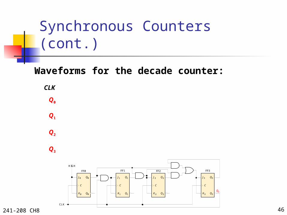
4-bit synchronous decade counter
With some additional logic, a binary counter can be converted to a BCD synchronous decade counter. After reaching the count 1001, the counter recycles to 0000.
CLK
J0
K0
C
HIGH
FF0 FF1 FF2 FF3
Q3
Q0
Q0
J1
K1
C
Q1
Q1
J2
K2
C
Q2
Q2
J3
K3
C
Q3
Q3
This gate detects 1001, and causes FF3 to toggle on the next clock pulse. FF0 toggles on every clock pulse. Thus, the count starts over at 0000. Q0
Q3
241-208 CH8 46
Synchronous Counters (cont.)
Waveforms for the decade counter:1 2 3 4 5 6 7 8
10 10 10 10 0
10 10 01010
00 11 01100
9 10
00 00 1 1000
1
0
0
0
0
0
0
0
CLK
Q0
Q1
Q2
Q3
CLK
J0
K0
C
HIGH
FF0 FF1 FF2 FF3
Q3
Q0
Q0
J1
K1
C
Q1
Q1
J2
K2
C
Q2
Q2
J3
K3
C
Q3
Q3

241-208 CH8 47
Synchronous Counters (cont.)
CTR DIV 16(1)
(9)
(7)
(10)
C(2)
(3) (4) (5) (6)
(14) (13) (12) (11)
TC = 15(15)
A 4-bit synchronous binary counter in IC form
The 74LS163 is a 4-bit IC synchronous counter with additional features over a basic counter. It has parallel load, a CLR input, two chip enables, and a ripple count output that signals when the count has reached the terminal count.Data inputs
Data outputs
CLR
LOADENTENPCLK
RCO
Q0 Q1 Q2 Q3
D0 D1 D2 D3
Both enable I/Ps
(Ripple Clock Output) goes high when count to state 15

241-208 CH8 48
Synchronous Counters (cont.)
Data inputs
Data outputs
CLR
LOAD
ENT
ENP
CLK
RCO
Q0
Q1
Q2
Q3
D0
D1
D2
D3
Clear Preset
Count Inhibit
12 13 14 15 0 1 2

241-208 CH8 49
Up/Down Synchronous Counters
•Counting in either direction (also called a bi-directional counter)
Says if u’d like to design a 3-bit up/down counter
Clock pulse Up DownQ2 Q1 Q0
01234567
00001111
00110011
01010101
Always toggle, hence J0=K0 =1
Down/ Q1 changes states when Q0=0
Up/ Q2 changes states when Q1&Q0=1
Up/ Q1 changes states when Q0=1
Down/ Q2 changes states when Q1&Q0=0

241-208 CH8 50
Up/Down Synchronous Counters (cont.)
CLK
Q0 Q1
Q2
K0
J
0
C C C
J
1
J
2
K1 K2
HIGH
UP/DOWN
UP
DOWN
FF0 FF1 FF2
Q0.DOWN
Q0 Q1 Q2
Basic 3-bit up/down synchronous counter

241-208 CH8 51
Up/Down Synchronous Counters (cont.)
The 74HC191 has the same inputs and outputs but is a synchronous up/down binary counter.
(10)(15)
(4)(5)
(11)(14)
(1) (9)
(3) (2) (6) (7)
(12)
(13)
Data inputs
Data outputs
MAX/MIN
CLK
Q0 Q1 Q2 Q3
LOAD
CTEN
RCO
D/U
D0 D1 D2 D3
C
CTR DIV 10
74HC190
(10)(15)
(4)(5)
(11)(14)
(1) (9)
(3) (2) (6) (7)
(12)
(13)
Data inputs
Data outputs
MAX/MIN
CLK
Q0 Q1 Q2 Q3
LOAD
CTEN
RCO
D/U
D0 D1 D2 D3
C
CTR DIV 16
74HC191
The 74HC190 is a high speed CMOS synchronous up/down decade counter with parallel load capability. It also has a active LOW ripple clock output (RCO) and a MAX/MIN output when the terminal count is reached.

241-208 CH8 52
Design of Synchronous CountersGeneral model of a sequential circuit

241-208 CH8 53
Design of Synchronous Counters (cont.)
001
011
010
110
100
101
111
000
Design procedure for synchronous counters
Step I: State diagram
Step II: Next state table:
Present State Next State
Q2 Q0
0 00 10 10 0
Q1
0011
1 011 111 101 00
Q2 Q0
0 10 10 01 0
Q1
0111
1 111 101 000 00
241-208 CH8 54
Design of Synchronous Counters (cont.)
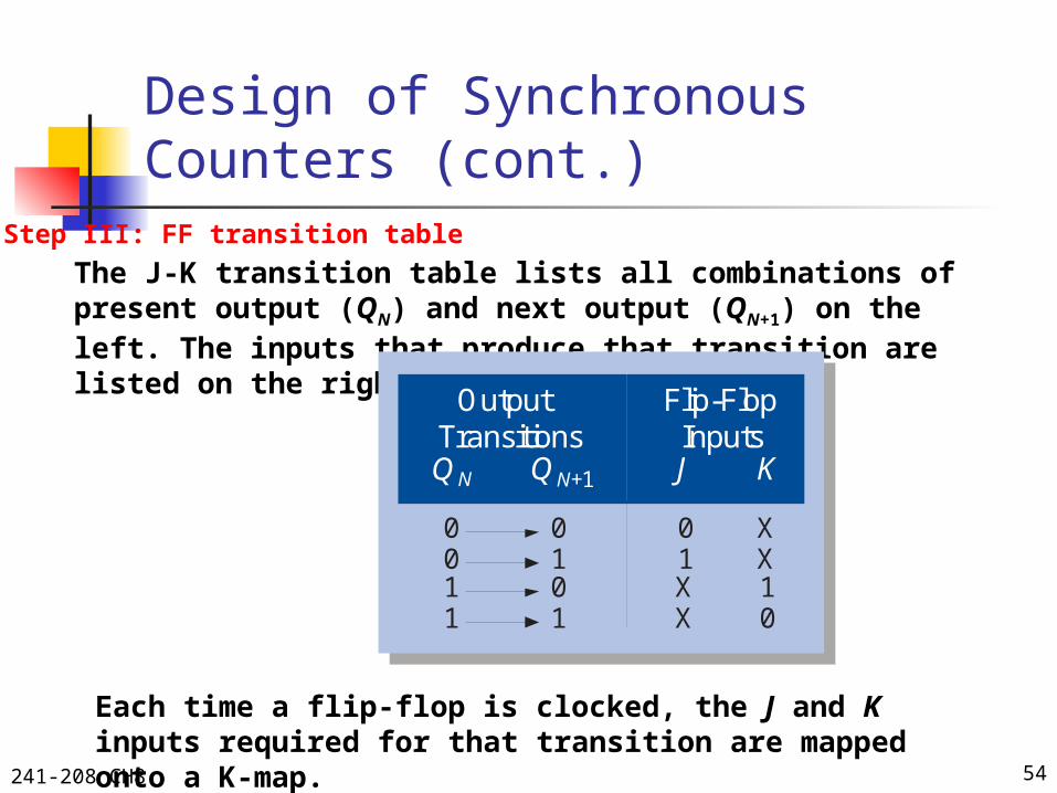
Step III: FF transition table
The J-K transition table lists all combinations of present output (QN) and next output (QN+1) on the left. The inputs that produce that transition are listed on the right.
Each time a flip-flop is clocked, the J and K inputs required for that transition are mapped onto a K-map.
OutputTransitions
Flip-FlopInputs
QN QN+1
0 00 11 01 1
J K
0 X1 XX 1X 0

241-208 CH8 55
Design of Synchronous Counters (cont.)
Step IV: K-maps
Example of mapping procedure

241-208 CH8 56
Design of Synchronous Counters (cont.)
Step IV: K-maps (cont.)
K-maps for present-state J&K inputs

241-208 CH8 57
Design of Synchronous Counters (cont.)
Step V: Logic expressions

241-208 CH8 58
Design of Synchronous Counters (cont.)
Step VI: Counter implementation
CLK
Q0 Q1
Q2
K0
J
0
C C C
J1 J
2
K1 K2
FF0 FF1 FF2
Q0 Q1 Q2
241-208 CH8 59
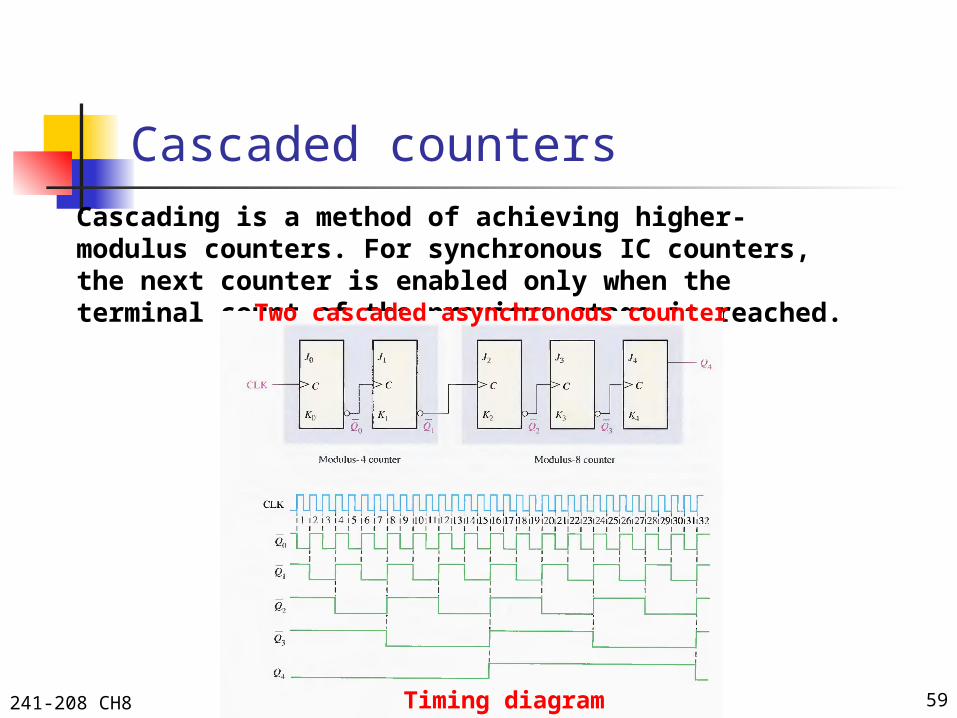
Cascaded counters Cascading is a method of achieving higher-modulus counters. For synchronous IC counters, the next counter is enabled only when the terminal count of the previous stage is reached.Two cascaded asynchronous counter
Timing diagram

241-208 CH8 60
Cascaded Counters (cont.)
16
ƒin
256
ƒin
HIGH
CLK Q0 Q1 Q2C
Counter 1 Counter 2
C
CTEN CTEN
CTR DIV 16 CTR DIV 16
Q3 Q0 Q1 Q2 Q3
TC TC
fin
fout
Modulus-256 synchronous counter using two cascaded synchronous counters

241-208 CH8 61
Counter Decoding
Decoding is the detection of a binary number and can be done with an AND gate. HIGH
CLK11 1
LSB MSB
Decoded 4
Q Q
Q
0 1
2
Q Q2 1 0Q
C
J2
K2
Q2
Q2
C
J1
K1
Q1
Q1
C
J0
K0
Q0
Q0
1.What number is decoded by this gate?
2. How to modify it in order to provide active-LOW decoding?

241-208 CH8 62
Counter Decoding (cont.)
Decoding glitches
BCD counter and decoder

241-208 CH8 63
Counter Decoding (cont.)
Way to eliminate glitches
BCD counter and decoder with strobing

241-208 CH8 64
Counter Applications
Digital clocks

241-208 CH8 65
Typical divide-by-60 Counter
CLR CTR DIV 6
HIGH CTEN
C
Q3
CTR DIV 10
Q2 Q1 Q0
CTEN TC = 9RCO
C
CLK
units
CLR CLR
To nextcounter
Q3 Q2 Q1 Q0
Decode 6
Decode 59
TC = 59To ENABLEof next CTR
tens
241-208 CH8 66
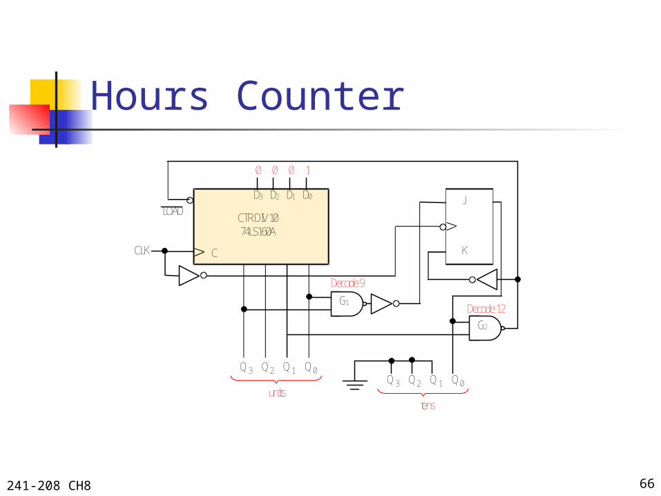
Hours Counter
LOAD
K
Q3
CTR DIV 1074LS160A
Q2 Q1 Q0
CCLK
units
J
Decode 9
Decode 12
tens
0 0 0 1
D3 D2 D1 D0
Q3 Q2 Q1 Q0
G1
G2

241-208 CH8 67
Counter Applications (cont.)
Automobile parking control

241-208 CH9 68
Basic Shift Register Functions A shift register is an arrangement of flip-flops with
important applications in storage and movement of data.
Data in Data in
Data in
Data in
Data in
Data out Data out Data out
Data out Data out
Serial in/shift right/serial out
Serial in/shift left/serial out Parallel in/serial out
Parallel in/parallel outSerial in/parallel out Rotate right Rotate left

241-208 CH9 69
Serial-in/Serial out Shift Register 5-bit serial in/serial out shift register
implemented with D flip-flops.
C
FF0
CLK
C
FF1
C
FF2
C
FF4
D0 D1 D2 D4
Serialdataoutput
Serialdatainput
C
FF3
D3 Q4Q0 Q1 Q2 Q3
1 1 1 1 1 1
CLK

241-208 CH9 70
Serial In/Parallel Out Shift Registers
4-bit serial in/parallel out shift register For example, assume the binary number
1011 is loaded sequentially, one bit at each clock pulse.
C
FF0
CLK
C
FF1
C
FF2
D0 D1 D2
Serialdatainput
C
FF3
D3Q0 Q1 Q2 Q31
C
FF0
CLK
C
FF1
C
FF2
D0 D1 D2
Serialdatainput
C
FF3
D3Q0 Q1 Q2 Q3
0 1
C
FF0
CLK
C
FF1
C
FF2
D0 D1 D2
Serialdatainput
C
FF3
D3Q0 Q1 Q2 Q3
1 0 1
C
FF0
CLK
C
FF1
C
FF2
D0 D1 D2
Serialdatainput
C
FF3
D3Q0 Q1 Q2 Q3
1 1 0 1
C
FF0
CLK
C
FF1
C
FF2
D0 D1 D2
Serialdatainput
C
FF3
D3Q0 Q1 Q2 Q3
1X 1 0 1
C
FF0
CLK
C
FF1
C
FF2
D0 D1 D2
Serialdatainput
C
FF3
D3Q0 Q1 Q2 Q31X 1 0 1
CLKCLKCLKCLK

241-208 CH9 71
74HC164A Shift Register
8-bit serial in/parallel out shift register One of the two serial data inputs may be used as an active HIGH enable
to gate the other input. If no enable is needed, the other serial input can be connected to Vcc. The 74HC164A has an active LOW asynchronous clear. Data is entered on the leading-edge of the clock.
(1)
(2)
(9)
(8)
S
C C C C
R
S S S S
C C C C
S S S
(3) (4) (5) (6) (10) (11) (12) (13)
R R R R R R R
CLK
Q0 Q1 Q2 Q3
CLR
Q4 Q5 Q6 Q7
Serial inputs
AB

241-208 CH9 72
Waveforms for the 74HC164A
B acts as an active HIGH enable for the data on A.
As with CMOS devices, unused inputs should always be connected to a logic level; unused outputs should be left open.
CLK
Q0
Q1
Q2
Q3
CLR
Q4
Q5
Q6
Q7
Serial inputs
A
B
Outputs
Clear Clear

241-208 CH9 73
Parallel In/Serial Out Shift Registers Shift registers can be used to convert
parallel data to serial form.
C
D
G2
C
D
G5
C
D
G3G6
C
D
G4G7G1
FF0 FF1 FF2 FF3
D0 D1 D2 D3
Q0 Q1 Q2 Q3
SHIFT/LOAD
CLK
Serial data out

241-208 CH9 74
74HC165 Shift Register 8-bit parallel in/serial out shift register The clock (CLK) and clock inhibit (CLK INH) lines are
connected to a common OR gate, so either of these inputs can be used as an active-LOW clock enable with the other as the clock input.
Data is loaded asynchronously when SH/LD is LOW and moved through the register synchronously whenSH/LD is HIGH and a rising clock pulse occurs.
C
SRG 8(1)
(10)
(15)(2)
(11) (12) (13) (14) (3) (4) (5) (6)(9)
(7)
D0 D1 D2 D3 D4 D5 D6 D7
Q7
Q7
SH/LD
CLK
SERCLK INH

241-208 CH9 75
74HC165 (cont.)

241-208 CH9 76
Parallel In/Parallel Out Shift Registers

241-208 CH9 77
Sample Timing Diagram

241-208 CH9 78
Bidirectional Shift Register
Bidirectional shift registers can shift the data in either direction using a RIGHT/LEFT input.

241-208 CH9 79
Example
How will the pattern change if the RIGHT/LEFT control signal is inverted?
CLKRIGHT/LEFTSerial data in
Q0
Q1
Q2
Q3
Shift right
Shift left

241-208 CH9 80
Example (cont.)
CLKRIGHT/LEFTSerial data in
Q0
Q1
Q2
Q3
Shift right
Shift leftShift right
Shift left

241-208 CH9 81
Universal Shift Register
A universal shift register has both serial and parallel input and output capability. The 74HC194 is an example of a 4-bit bidirectional universal shift register.
(1)
(15) (14) (13) (12)
(3) (4) (5) (6)
(9)
(10)
(2)
(7)
(11)C
SRG 4
D0 D1 D2 D3
CLK
SL SER
Q0 Q1 Q2 Q3
SR SER
S1
S0
CLR
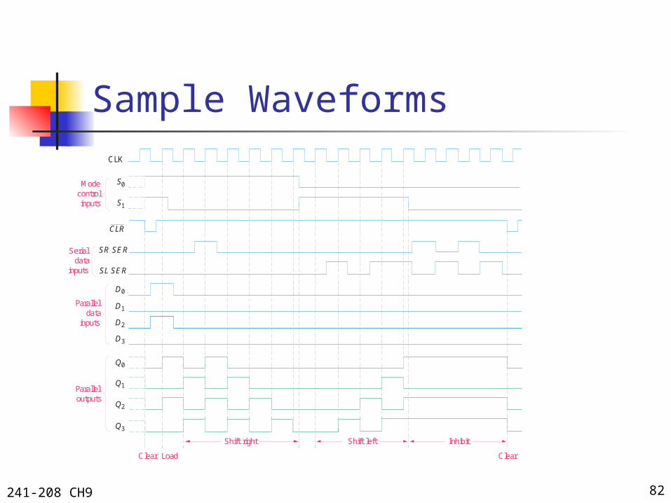
241-208 CH9 82
Sample Waveforms
Paralleldata
inputs
Shift right
Modecontrolinputs
Paralleloutputs
Clear Load
Shift left Inhibit
Clear
CLR
S1
SR SER
SL SER
D0
D1
D2
D3
Q0
Q1
Q2
Q3
S0
CLK
Serialdata
inputs

241-208 CH9 83
Shift Register Counters
C
Q0
FF0
CLK
C
Q1
FF1
C
FF2
C
Q3
FF3
D0 D1 D2 D3Q2
Q3 Q3
Shift registers can form useful counters by recirculating a pattern of 0’s and 1’s. Two important shift register counters are the Johnson counter and the ring counter.
The Johnson counter can be made with a series of either D flip-flops or J-K flip-flops.
C
Q0
FF0
CLK
C
Q1
FF1
C
FF2
C
Q3
FF3
J 0 J 1 J 2 J 3Q2
Q0 Q1K0 K1 K2 K3Q2 Q3
Q
Q
3
3

241-208 CH9 84
Johnson counter The Johnson counter is useful when you need a sequence
that changes by only one bit at a time but it has a limited number of states (2n, where n = number of stages).The first five counts for a 4-bit Johnson counter that is
initially cleared are: CLK Q0 Q1 Q2 Q3 0 0 0 0
1 0 0 01 1 0 01 1 1 01 1 1 10 1 1 1 0 0 1 1 0 0 0 1
01234567What are the remaining 3
states?

241-208 CH9 85
Ring Counter The ring counter can also be implemented
with either D flip-flops or J-K flip-flops. 4-bit ring counters are constructed from a
series of D flip-flops and J-K flip-flops. Notice the feedback.
C
Q0
FF0
CLK
C
Q1
FF1
C
FF2
C
Q3
FF3
D0 D1 D2 D3Q2
Q3
C
Q0
FF0
CLK
C
Q1
FF1
C
FF2
C
Q3
FF3
J 0 J 1 J 2 J 3Q2
Q0 Q1K0 K1 K2 K3Q2 Q3
Q
Q
3
3
Describe the disadvantage and advantage of the ring counter?

241-208 CH9 86
Ring Counter
1 2 3 4 7 8 9 105 6CLK
Q0
Q1
Q3
Q4
Q2
Q5
Q6
Q7
A common pattern for a ring counter is to load it with a single 1 or a single 0. The waveforms shown here are for an 8-bit ring counter with a single 1.

241-208 CH9 87
Shift Register Applications Examples: Time Delay, Parallel/Serial Data Converter, and
Keyboard Encoder
Q7
Q7
A
BData out
CLK40 MHz
Data in
CLK
Data in
Data outtd
C
SRG 8
An 8-bit serial in/serial out shift register has a 40 MHz clock. What is the total delay through the register?
The delay for each clock is 1/40 MHz = 25 nsThe total delay is 8 x 25 ns = 200 ns
25 ns
= 200 ns

241-208 CH9 88
Parallel/Serial Data Converter
D7 D6 D5 D4 D3 D2 D1 D0t
Start
Bit (0)Stop Bits (1)

241-208 CH9 89
Parallel/Serial Data Converter (cont.)
241-208 CH9 90
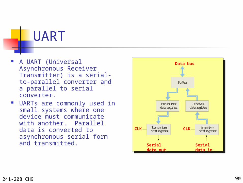
UART
A UART (Universal Asynchronous Receiver Transmitter) is a serial-to-parallel converter and a parallel to serial converter.
UARTs are commonly used in small systems where one device must communicate with another. Parallel data is converted to asynchronous serial form and transmitted.
Data bus
Serial data inSerial data out
CLK CLK
Receiverdata register
Transmitterdata register
Buffers
Transmittershift register
Receivershift register

241-208 CH9 91
Keyboard Encoder
The keyboard encoder is an example of where a ring counter is used in a small system to encode a key press.
Two 74HC195 shift registers are connected as an 8-bit ring counter preloaded with a single 0.
As the 0 circulate in the ring counter, it “scans” the keyboard looking for any row that has a key closure.
When one is found, a corresponding column line is connected to that row line.

Q0 Q1 Q2 Q3 Q4 Q5
D0 D1 D2 D3 D4 D5
Q5 Q6 Q7Q4Q1 Q2 Q3
D4 D5 D6 D7D1 D2 D3
Q
COLUMN encoder74HC147
1 2 3 4 5 6 7 8
1 2 4
ROW encoder74HC147
1 2 3 4 5 6 7 8
1 2 4
Key code register74HC174
QC
Clock inhibit
+V
One-shots To ROM
Switch closure
Q
D0
Q0
JK
C
SRG 474HC195
JK
C
SRG 474HC195CLK
(5 kHz)
Power on LOADSH/LD +VCC
Ring counter
CC

241-208 CH7 93
Conclusion
•ET FFs is a synchronous bistable device, whose state depends on the input only at the triggering transition of a clock pulse
•JK-FFs is mostly used since we can design other FF types (D,RS) with JK-FF.
•Applications of FFs are frequency division, counter, and storage device.