3-d simulation of si-prot charge distribution, signal development d. attié, p. colas, e. delagnes,...
TRANSCRIPT

3-D simulation of Si-ProtCharge distribution, signal development
D. Attié, P. Colas, E. Delagnes, S. Turnbull
- Introduction
- Orders of magnitude
- Simulation
- Results
- Data
April 17, 2008 RD51 workshop 2
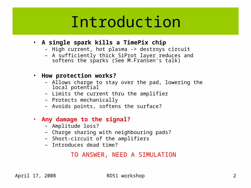
Introduction• A single spark kills a TimePix chip
– High current, hot plasma -> destroys circuit– A sufficiently thick SiProt layer reduces and softens the sparks
(See M.Fransen’s talk)
• How protection works? – Allows charge to stay over the pad, lowering the local potential– Limits the current thru the amplifier– Protects mechanically– Avoids points, softens the surface?
• Any damage to the signal?– Amplitude loss?– Charge sharing with neighbouring pads?– Short-circuit of the amplifiers– Introduces dead time?
TO ANSWER, NEED A SIMULATION

April 17, 2008 RD51 workshop 3
Orders of magnitude
R neighbour
R thru
e
lL
Rneighb = L/el = /e for square pads
For 10 µ aSi, =1011 .cm, R=1014 /square
Rthru = e/Ll ~ 0.04 1014
Rneighb/Rthru = L2/e2
e<<L to avoid spreading the charge by side conductivity. The charge preferentially escapes thru the pad, but with an extremely high resistance.
Cneighb = r Le/l =r /e for square pads
Cthru = r Ll/e (note r ~11 for Si)
The influence acts preferentially thru the pad if L>>e
April 17, 2008 RD51 workshop 4
R neighbour
R thru
e
lL
Also Rthru >> 1/C to leave the induced signal
(OK with 1011 cm within 3 orders of magnitude for 10 ns signals)
Equivalently, RC time constant >> 10ns
The signal is fully capacitive
1/Cthru
1/Cneighbour

5 pixels
5 pixels
gas
Siprot
25 Pads
25 TimePixPreamps
gas: 10x10x10elements/pad
SiProt: 10x10x10elements/pad
« central » gas element.C network
(special ones fo edges)
« central » SiProt elementRC network
(special ones fo edges)Pads:Metallisation of the last SiProt elements
« Full » shape100% of pixel
aluminized
« Cross » shape12% of pixel Al,
rest SiN2
Charge Injection at the gas / SiProt interface in the central pixel Size = 4 elts 3 positions.
Top= HT (ac grounded)
1
23
SiProt Simulation with Analog ArtistE. Delagnes, S.Turnbull
April 17, 2008 RD51 workshop 6
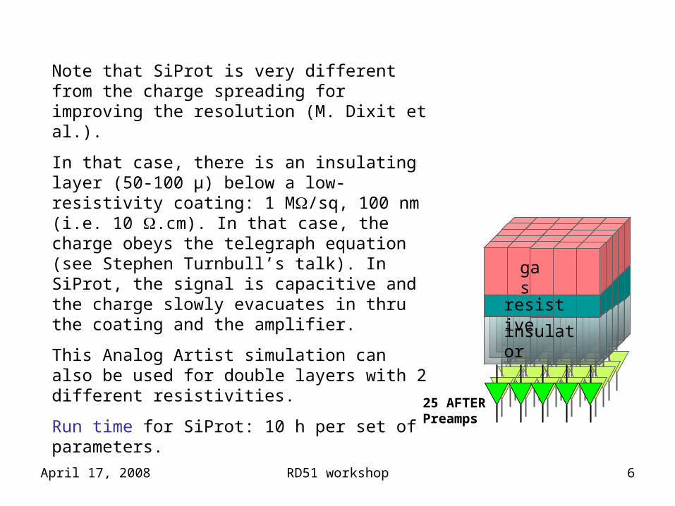
Note that SiProt is very different from the charge spreading for improving the resolution (M. Dixit et al.).
In that case, there is an insulating layer (50-100 µ) below a low-resistivity coating: 1 M/sq, 100 nm (i.e. 10 .cm). In that case, the charge obeys the telegraph equation (see Stephen Turnbull’s talk). In SiProt, the signal is capacitive and the charge slowly evacuates in thru the coating and the amplifier.
This Analog Artist simulation can also be used for double layers with 2 different resistivities.
Run time for SiProt: 10 h per set of parameters.
25 AFTERPreamps
gas
resistive
insulator

April 17, 2008 RD51 workshop 7
Signal development Charge pulse: 1ns trapezoidal current pulse
Small Cross vs Large Pads; Timepix Chip Simulation, 15um resistive layer.
-9,00E-04
4,91E-02
9,91E-02
1,49E-01
1,99E-01
2,49E-01
2,99E-01
3,49E-01
0,00E+00 1,00E-06 2,00E-06 3,00E-06 4,00E-06 5,00E-06 6,00E-06
Time (s)
Hig
h (
un
its
)
12 13 14 18 19 20 21 24 12 full 13 full
Injection in the middle
Injection in the corner
Injection in between
April 17, 2008 RD51 workshop 8
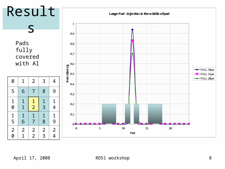
ResultsLarge Pad : injection in the middle of pad
0
0,1
0,2
0,3
0,4
0,5
0,6
0,7
0,8
0,9
1
0 5 10 15 20
Pad
Norm
aliz
ed s
ignal
FULL 10µm
FULL 15µm
FULL 20µm
0 1 2 3 4
5 6 7 8 9
10 11 12 13 14
15 16 17 18 19
20 21 22 23 24
Pads fully covered with Al

April 17, 2008 RD51 workshop 9
Results
0 1 2 3 4
5 6 7 8 9
10 11 12 13 14
15 16 17 18 19
20 21 22 23 24
"Cross" Pad : injection in the middle of pad
0
0,1
0,2
0,3
0,4
0,5
0,6
0,7
0,8
0,9
1
0 5 10 15 20
Pad
Norm
aliz
ed s
ignal
Cross 10µm
Cross 15µm
Cross 20µm
Pads 12% covered.
April 17, 2008 RD51 workshop 10
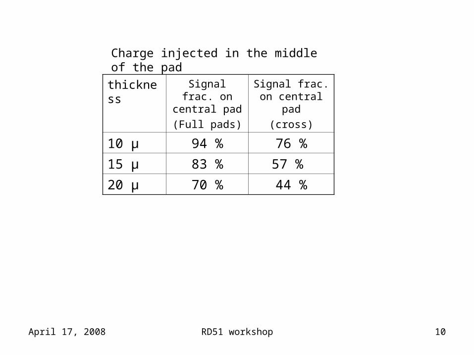
thickness Signal frac. on central pad
(Full pads)
Signal frac. on central pad
(cross)
10 µ 94 % 76 %
15 µ 83 % 57 %
20 µ 70 % 44 %
Charge injected in the middle of the pad

April 17, 2008 RD51 workshop 11
PRFs
0
0,1
0,2
0,3
0,4
0,5
0,6
0 0,5 1 1,5 2 2,5 3 3,5 4
distance of injection from pad center (in fraction of pad pitch)
Mea
sure
d C
har
ge Full 10µm
Cross 10µm
Full 15µm
Cross 15µm
Full 20µm
Cross 20µm
Pad Response Function

April 17, 2008 RD51 workshop 12
Data
• With 20 µ SiProt, the spreading over several pads is clearly seen, but the grid misalignment also contributes.
April 17, 2008 RD51 workshop 13
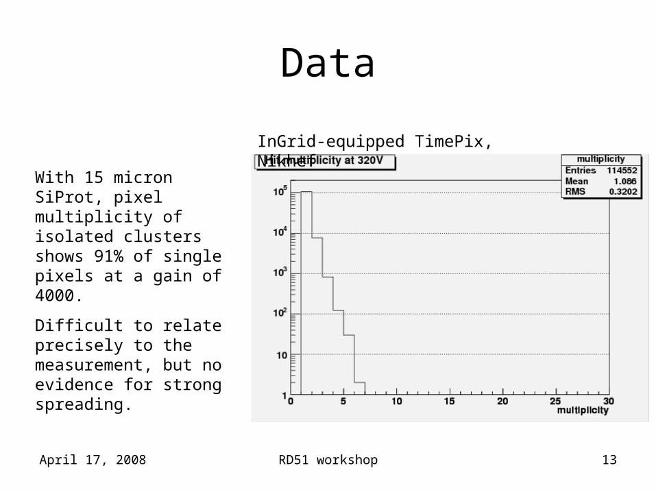
Data
With 15 micron SiProt, pixel multiplicity of isolated clusters shows 91% of single pixels at a gain of 4000.
Difficult to relate precisely to the measurement, but no evidence for strong spreading.
InGrid-equipped TimePix, Nikhef

April 17, 2008 RD51 workshop 14
Conclusions• Charge spreading is limited both in space and
time for SiProt thickness less than 10-15 m.• Fully covered anodes spread less than partially
covered anodes
• SaclayDavid Attié
Max Chefdeville
Paul Colas
Xavier Coppolani
Eric DelagnesArnaud GiganonIoannis Giomataris
Marc Riallot
Stephen Turnbull
• CERNMichael CampbellXavier Llopart
• NikhefYevgen BilevychMarten BosmaMax ChefdevilleMartin Fransen Fred HartjesJan Timmermans Harry van der Graaf Jan Visschers
TimePix-Micromegas collaboration