458 ieee journal of selected topics in quantum electronics...
TRANSCRIPT

458 IEEE JOURNAL OF SELECTED TOPICS IN QUANTUM ELECTRONICS, VOL. 17, NO. 2, MARCH/APRIL 2011
Integrated Photonics for Low-PowerPacket Networking
Daniel J. Blumenthal, Fellow, IEEE, John Barton, Neda Beheshti, John E. Bowers, Fellow, IEEE, Emily Burmeister,Larry A. Coldren, Fellow, IEEE, Matt Dummer, Garry Epps, Alexander Fang, Yashar Ganjali, Member, IEEE,
John Garcia, Brian Koch, Vikrant Lal, Erica Lively, John Mack, Milan Masanovic, Nick McKeown, Fellow, IEEE,Kim Nguyen, Steven C. Nicholes, Hyundai Park, Biljana Stamenic, Anna Tauke-Pedretti,
Henrik Poulsen, and Matt Sysak
(Invited Paper)
Abstract—Communications interconnects and networks willcontinue to play a large role in contributing to the global carbonfootprint, especially in data center and cloud-computing applica-tions exponential growth in capacity. Key to maximizing the bene-fits of photonics technology is highly functional, lower power, andlarge-scale photonics integration. In this paper, we report on thelatest advances in the photonic integration technologies used forasynchronous optical packet switching using an example photonicintegrated switched optical router, the label switched optical router
Manuscript received May 12, 2010; revised July 1, 2010; accepted April3, 2010. Date of publication January 12, 2011; date of current version April6, 2011. This work was supported in part by Defense Advance ResearchProject Agency Office of Microsystems Technology (DARPA/MTO) Datain the Optical Domain (DODN) Program under Award W911NF-04-9-0001and DARPA/MTO Chip Scale Wavelength Division Multiplexing (CSWDM)Program under Award N66001-02-C-8026.
D. J. Blumenthal, J. Barton, J. E. Bowers, L. A. Colden, J. Garcia, E. Lively,M. Masanovic, K. Nguyen, B. Stamenic, and H. Poulsen are with the Universityof California, Santa Barbara, CA 93106 USA (e-mail: [email protected];[email protected]; [email protected]; [email protected];[email protected]; [email protected]; [email protected];[email protected]; [email protected]; [email protected]).
N. Beheshti was with the Department of Computer Science, StanfordUniversity, Palo Alto, CA 94305 USA, and is now with Ericsson Research Lab,San Jose CA 95134. USA (e-mail: [email protected]).
E. Burmeister and M. Dummer were with the University of California, SantaBarbara, CA 93106 USA. They are now with Ciena Corporation, Linthicum,MD 21090 USA (e-mail: [email protected]; [email protected]).
G. Epps is with Cisco Systems, Inc., San Jose, CA 95134 USA (e-mail:[email protected]).
A. Fang and S. C. Nicholes are with Aurrion, Santa Barbara, CA 93117 USA(e-mail: [email protected]; [email protected]).
Y. Ganjali was with the Stanford University, Palo Alto, CA 94305 USA. Heis now with the University of Toronto, Toronto, ON M5S 1A1, Canada (e-mail:[email protected]).
B. Koch is with the Photonics Technology Labs, Intel Corporation, SantaClara, CA 95054 USA (e-mail: [email protected]).
V. Lal is with the Infinera Corporation, Sunnyvale, CA 94089 USA (e-mail:[email protected]).
J. Mack was with the Department of Electrical and Computer Engineering,University of California, Santa Barbara, CA 93106 USA. He is now with theLaboratory for Telecommunications Sciences, University of Maryland CollegePark (e-mail: [email protected]).
N. McKeown is with the Stanford University, Palo Alto, CA 94305 USA(e-mail: [email protected]).
H. Park and M. Sysak were with the Department of Electrical andComputer Engineering, University of California, Santa Barbara, CA 93106USA. They are now with Intel Corp. (e-mail: [email protected];[email protected]).
A. Tauke-Pedretti is with Sandia National Laboratories, Albuquerque, NM5800 USA (e-mail: [email protected]).
Color version of one or more of the figures in this paper are available onlineat http://ieeexplore.ieee.org.
Digital Object Identifier 10.1109/JSTQE.2010.2077673
architecture. We report measurements of the power consumed bythe photonic circuits in performing their intended function, theelectronics required to bias the photonics, processing electronics,and required cooling technology. Data is presented to show thatthere is room (potentially greater than 10 ×) for improvement inthe router packet-forwarding plane. The purpose of this exercise isnot to provide a comparison of all-optical versus electronic routers,rather to present a data point on actual measurements of the powercontributions for various photonic integration technologies of anall-optical packet router that has been demonstrated and conclude,where the technology can move to reduce power consumption forhigh-capacity packet routing systems.
Index Terms—Optical communications, optical packet switching,photonic integration.
I. INTRODUCTION
THE predicted carbon footprint of data communicationsnetworks and data centers to the global IT sector con-
tributes almost one-half of the total expected contribution. Withpredicted exponential growth in capacity due to consumer ap-plications like video demand taking off, technologies that cansave power in the network communications, and data center in-frastructures will be critical. Photonics has the potential basedon fundamentally different power scaling laws, to enable highcapacity and bandwidth systems to scale in a different man-ner than how systems are architected today based on electronicintegrated technologies. The power savings from using photon-ics technologies will need to come about from rearchitectingthese systems as well as pushing the state of the art in pho-tonic integration. In this paper, we focus on results from theDARPA-funded label switched optical router (LASOR) projectto illustrate how photonics can be used to offset power andfootprint limits that will be imposed for high-capacity futurerouters and communications system. We will describe how theLASOR project systematically addresses, through design andmeasurements, the largest power consumer in today’s router ar-chitectures as the fiber bit rate and router capacity increases. Wewill also describe how photonic circuits, positioned in the properfunctions in a packet-based system provide better power scalingbehavior as the line bit rate increases relative to electronic solu-tions that rely on heavy parallelism and fast transistors. In orderto begin to understand, the potential photonic ICs (PICs) canhave on the power consumption of packet switched systems, it
1077-260X/$26.00 © 2011 IEEE

BLUMENTHAL et al.: INTEGRATED PHOTONICS FOR LOW-POWER PACKET NETWORKING 459
Fig. 1. Contributions of IT sectors to the global carbon footprint.
Fig. 2. Intel study showing the dominant contribution of communicationsequipment in data centers to the heat load per product footprint [1].
is important to build and measure prototype systems based onreal PIC technologies.
II. CARBON FOOTPRINT OF IT SYSTEMS
IT systems continue to increase demands on energy suppliesas computer usage, network bandwidth, data storage, and ap-plications continue to increase at an ever-expanding rate. Theproblem has become quite severe, on the order of other ma-jor global emissions contributors including the global aviationindustry. A study done on the global footprint by subsector in2009, shown in Fig. 1, demonstrates the impact of PCs, periph-erals and printer, and the telecommunications and data centerinfrastructures. The global telecommunications and data centerinfrastructures are expected to subsume almost half of the ITcontributions to carbon footprint.
The heat-load contributions to data centers as a function ofdata centers release date was reported by Intel and is shownin Fig. 2, where the breakdown of the heat load per footprintillustrates that communications equipment continues to be anincreasingly dominant contribution. New technologies, such asphotonics, have the potential to flatten out or reduce this growthwhen architected properly into systems and integrated usingnext generation photonics integrated technologies, as discussedfurther on.
III. POWER LIMITATIONS OF TODAY’S COMMUNICATIONS
SYSTEMS—SYSTEM SCALABILITY AND THE
POWER SPREADING PROBLEM
The energy problem due to the communications infrastructurewill grow as continued increase in IP traffic growth pushesdemands on communications equipment. As shown in Fig. 3increases in IP traffic growth due in particular to consumer
Fig. 3. Projected IP traffic growth due to video and new high band-width demands (Graphs courtesy of Cisco Visual Networking Index http://www.cisco.com/en/US/netsol/ns827/networking_solutions_sub_solution.html).
demand for services like video are projected to increase by afactor of fivefold by 2013.
The system bandwidth of high-capacity systems that needto support this growth, like routers, data centers, and telecom-munications infrastructure, rely on continued improvements inelectronic technologies in terms of metrics like megahertz-gateper milliwatt and megabits per second per watt in order to keepthe system power flat, while providing for continual scaling insystem bandwidth (BW).
As shown in Fig. 4, the power/performance efficiency im-provements of high-performance electronic communication

460 IEEE JOURNAL OF SELECTED TOPICS IN QUANTUM ELECTRONICS, VOL. 17, NO. 2, MARCH/APRIL 2011
Fig. 4. Historical growth of high-end router capacity and improvements inpower efficiency (relative to products of 1993) and dependence on continuedimprovements in electronic component efficiency.
systems are bound to the efficiency improvements of the un-derlying silicon technology. To scale systems at a higher ratethan the component technology requires architectural innova-tion and/or a compromise in one or more areas of systemfunctionality such as performance, programmability, or phys-ical size/density. However, this architectural workaround is dif-ficult to sustain long-term and fundamental improvements inthe underlying technology is required to overcome projectedshortfalls.
The capacity of single-rack Internet routers has grown byapproximately threefold every 18 months and is limited by thepower that can be delivered to, and dissipated from, a singlerack of equipment. Power consumption has grown with ca-pacity, and the largest single-rack routers today consume over10 kW. Architecting electronic core routers with higher capaci-ties continues to burden all aspects of system design and under-lying technologies including switch fabric capacity and packetprocessing, such as forwarding, queuing, and buffering. Today’sstate-of-the-art core routers utilize multirack designs in orderto spread the system power over multiple racks, reducing thepower density, and push aggregate capacities to 100 s of Tb/s.However, these systems require as many as six optoelectronicconversions per input/output and multirack configurations dom-inated by interface cards. For example, a 25 Tb/s router with 12840 Gb/s I/O ports can require 768 40Gb/s actual or equivalentoptoelectronic/electrooptic (OE/EO) conversions, whose powerdissipation and footprint increase with number of ports and bitrate per port.
One reason for the tradeoff in system BW (where systemBW is defined as router capacity or throughput with a givenpacket loss rate and offered load at the input) with physicalsize/density even with faster and denser electronics is related tothe power-spreading problem, as illustrated in Fig. 5. Today’stransistors exhibit a fixed leakage current that is based on currentmanufacturing technology pervasive in the existing semiconduc-tor processing foundry infrastructure that is very expensive tochange on a large-scale basis even with fundamental improve-ments in transistor technology. Additionally, running transistorsat ever increasingly high clock speeds adds to the power dis-
Fig. 5. Effect of power-spreading problem on system footprint and powerdissipation.
Fig. 6. Scaling of switching energy as a function of the size of switchedinformation for photonics versus electronics.
sipation problem making multicore solutions more desirable.Since the power footprint of a system is practically constrained,single-chip solutions quickly become multichip solutions withan added power overhead for interchip communications, fol-lowed by the need to move to multiline card and multiracksolutions, each with additional added communications poweroverhead between cards, shelves, and racks.
IV. POTENTIAL IMPACT OF PHOTONICS
ON POWER SCALING LAWS
Photonics has the potential to change the power scaling lawsof high bandwidth systems through proper architectural choicesthat combine photonics with electronics to optimize perfor-mance, power, footprint, and cost. The major types of datain a communications system are shown in Fig. 6 with circuitswitching at one extreme of granularity and packet switchingat the other extreme. Traditionally, digital electronics is used toswitch these data units, and transistors must switch and expendenergy at the bit rate for every bit. The faster the bit rate, themore energy is expended per bit and the longer the task themore energy is expended per task (e.g., circuit, burst (includingpacket flows), and packet).
Using analog photonics to switch or tasks requires switchingonly at the task boundaries. However, there does exist a tradeoffbetween the switching energy and the bias power depends onthe photonics technology used. While electronics has very lowswitching energy and bias power, certain photonics technolo-gies, like microelectromechanical system (MEMS) can havelower bias power while other technologies like semiconduc-tor optical amplifiers (SOAs) require higher bias powers today.The tradeoff between initial bias power, switching energy, and
BLUMENTHAL et al.: INTEGRATED PHOTONICS FOR LOW-POWER PACKET NETWORKING 461
Fig. 7. Energy used to switch task for electronics and photonics as a functionof task length.
switching at the bit level or task boundary leads to qualitativebehaviors illustrated in Fig. 6. Today’s photonics and electronicsdissipate roughly the same power for smaller tasks. The totalbit level switching energy per task dominates the bias power forlonger task for electronics as is shown in the curve “extendingtoday’s OE optic (OEO) technology.” As the bit rate is increasedfor electronics, the power to switch transistors increases and thetask curve moves to the left approaching Moore’s law limit.Photonics (analog) has a qualitatively different behavior, wherethe energy per task is dominated by the bias power and does notincrease significantly as the bit rate and task length increases.This is shown qualitatively in the photonics limit curve in Fig. 7.It is important to note that the curves in Fig. 7 represent switch-ing in the data plane and do not include a dominant componentof processing packet forwarding or connection setup.
V. EXAMPLE SYSTEM-–LASOR: A LABEL
SWITCHED OPTICAL ROUTER
For purposes of the power analysis of PIC for this paper, theLASOR project [1], [3]–[5], funded by DARPA MTO, is pre-sented as an example optical packet switching system, where thepower dissipation of the integrated photonics and surroundingelectronics has been quantified. The purpose of this exercise isnot to provide a firm comparison of all-optical versus electronicrouters as this is a very complex and problem with rapidly mov-ing data points. The purpose of this paper is rather to presenta data point on actual measurements of the power contribu-tions for various components of an all-optical packet router thathas been demonstrated and conclude, where the technology canmove to.
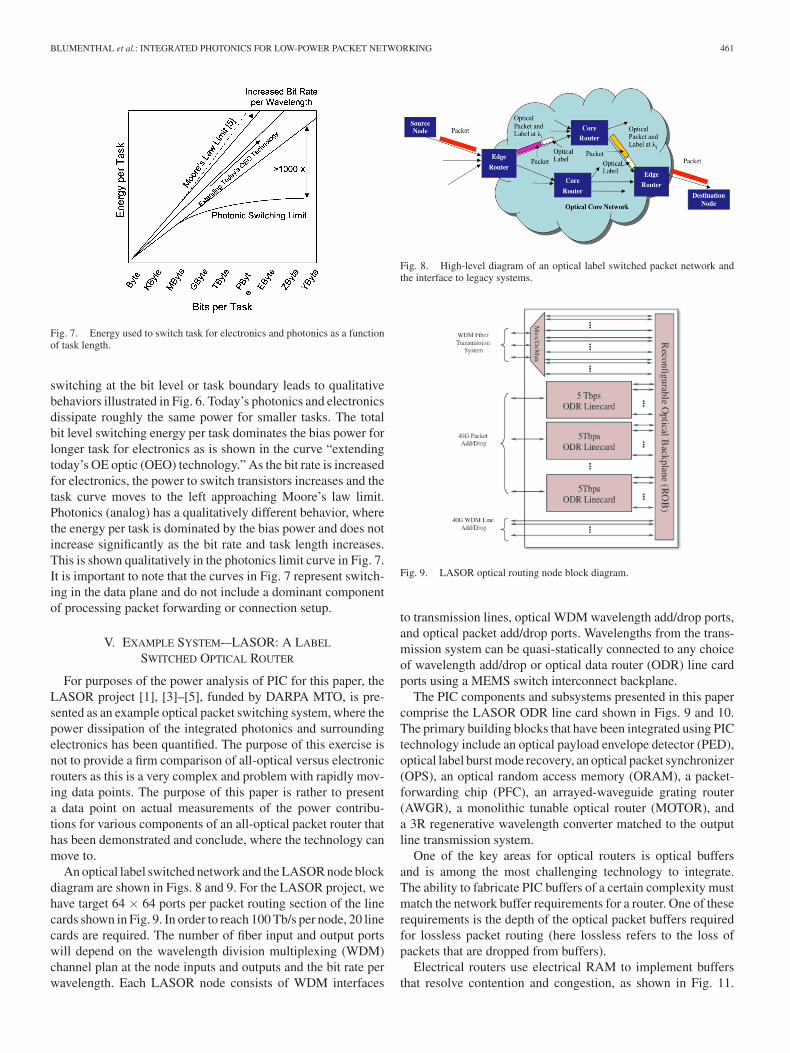
An optical label switched network and the LASOR node blockdiagram are shown in Figs. 8 and 9. For the LASOR project, wehave target 64 × 64 ports per packet routing section of the linecards shown in Fig. 9. In order to reach 100 Tb/s per node, 20 linecards are required. The number of fiber input and output portswill depend on the wavelength division multiplexing (WDM)channel plan at the node inputs and outputs and the bit rate perwavelength. Each LASOR node consists of WDM interfaces
Fig. 8. High-level diagram of an optical label switched packet network andthe interface to legacy systems.
Fig. 9. LASOR optical routing node block diagram.
to transmission lines, optical WDM wavelength add/drop ports,and optical packet add/drop ports. Wavelengths from the trans-mission system can be quasi-statically connected to any choiceof wavelength add/drop or optical data router (ODR) line cardports using a MEMS switch interconnect backplane.
The PIC components and subsystems presented in this papercomprise the LASOR ODR line card shown in Figs. 9 and 10.The primary building blocks that have been integrated using PICtechnology include an optical payload envelope detector (PED),optical label burst mode recovery, an optical packet synchronizer(OPS), an optical random access memory (ORAM), a packet-forwarding chip (PFC), an arrayed-waveguide grating router(AWGR), a monolithic tunable optical router (MOTOR), anda 3R regenerative wavelength converter matched to the outputline transmission system.
One of the key areas for optical routers is optical buffersand is among the most challenging technology to integrate.The ability to fabricate PIC buffers of a certain complexity mustmatch the network buffer requirements for a router. One of theserequirements is the depth of the optical packet buffers requiredfor lossless packet routing (here lossless refers to the loss ofpackets that are dropped from buffers).
Electrical routers use electrical RAM to implement buffersthat resolve contention and congestion, as shown in Fig. 11.

462 IEEE JOURNAL OF SELECTED TOPICS IN QUANTUM ELECTRONICS, VOL. 17, NO. 2, MARCH/APRIL 2011
Fig. 10. Main components of the 8 × 8 LASOR ODR. The wavelength con-version (WC) element is the PFC PIC and the buffer is the ORAM PIC describedin the following.
Fig. 11. Buffering in a combined input/output queuing (CIOQ) router. Inputbuffers store packets when there is internal contention. Output buffers storepackets when output links are congested.
Fig. 12. Link utilization versus input and output buffer sizes. With 25 Mb/saccess links, five-packet virtual output queues (VOQs) and 15-packet outputbuffers make the utilization above 80%.
This capacity is currently not feasible with any proposed opticalbuffering approach. But research has shown that much smallerbuffering capacities are adequate, on the order of 10–20 packetdeep buffers, within the reach of today’s PIC technology. Anal-ysis, simulations, and experiments show that if access links runslower than backbone links, the traffic is smoothed, and hence,only 10–20 packet buffers per output port are needed for 80%throughput, as shown in Fig. 12 [6]–[8].
Fig. 13. Enabling technologies to allow for future photonic integration.
Fig. 14. All-photonic PICs using the SAM and CAM approach.
VI. LOW-POWER PICS
Photonic integration has the potential to save power for packetrouting systems and other applications. However, in order forPIC technology to make in-roads to real systems and be anenergy efficient, cost effective, and manufacturable technologythat scales to a large number of on-chip components, multi-ple key issues must be addressed [9]–[11]. As shown in figure,new generation of PICs will require advances in ultralow powersources, detectors and amplifiers, ultralow-loss waveguides andinterconnects, ultrahigh density components, digitally regener-ative optics, efficient integration of electronics and photonics,and low cost packaging and manufacturing as well as high-yieldPICs (see Fig. 13).
Under the LASOR program, we have investigated two cate-gories of all-photonic devices, as depicted in Fig. 14. We definea spread of approaches to lie along a line that has OEO that liesat one extreme. We define OEO, where not only are photonsconverted to electrons and vice versa, but digital manipulation,using electronic transistors or logic gates, occurs between theoptical input and output. We define three subcategories of all-photonic, where the first two, photocurrent-driven wavelengthconverters (SAM) and concurrent absorption and modulationwavelength converters (CAM) involve interactions of photonswith free carriers and the third involves interaction of photonswith bound carriers. The term all-photonic is used for all-optical,CAM, and SAM, since all processes that involve photons con-trolling photons involve intermediate interaction with electrons,either bound or free.

BLUMENTHAL et al.: INTEGRATED PHOTONICS FOR LOW-POWER PACKET NETWORKING 463
TABLE ILASOR PIC FUNCTIONS AND PERFORMANCE
SAM devices utilize separate absorption and modulation sec-tions, where the input light is absorbed/detected and used toremodulate the light onto a new optical signal via an exter-nally modulated laser and these two sections are connectedby a simple wire or electron waveguide. CAM devices utilizecolinear optical and electronic waveguides, where the input pho-tons directly interact with electrons as in a SOA to produce amodulation effect transferring the input optical data onto a newoutbound optical signal. Bound carrier devices utilize nonlin-ear polarization interaction between the photon and a boundelectron to produce new optical signals, such as with four-wavemixing in optical fibers or second harmonic generation in, e.g.,lithim niobate.
In this paper, we focus on two types of all-photonic PICsintegrated under the LASOR project, the SAM and CAM types.Table I lists the PIC devices that are covered in this paper, theintegration platform used, a performance summary and list ofrelevant references for each.
Fig. 15. All-optical PED principal, operation and PIC.
A. Optical PED
The PED function [12] is used to determine the locationof the optical packet boundaries with high precision withoutprocessing the individual bits, saving power as the length of thepacket increases and the bit rate increases.
The PED output is used to create a precise time reference ofthe payload in the electrical domain relative to the optical do-main in order to make synchronization, buffering, label erasureand rewrite, and forwarding operations.
An all-photonic CAM implementation of the PED functionprovides very rapid rise and fall times of the envelope signalas well as low jitter. A discrete all-optical PED implementationalong with on optical packet and the resulting optical envelopeis shown in Fig. 15(a). Integration of the optical PED functiononto a monolithic chip is shown in Fig. 15(b) [13]. The compo-nents are similar to those used in the PFC and the optical clockrecovery chip.
B. Burst-Mode Optical Clock and Data Recovery
The task of recovering and processing headers in an asyn-chronous optical packet switching system poses many uniquechallenges. At each node input, the optical packet arrival timeand the optical packet length are not known ahead of time. Inthe LASOR system, optical packets consist of payloads thatare preceded by optical headers used to compute forwardingand new header information at each node. In order to processthe optical headers using electronics, the header clock and datamust be recovered burst mode (asynchronously) with a mini-mum of overhead bits (preamble). The recovered clock phaseand frequency accuracy must result in error-free label recoveryor the packet will be incorrectly routed. A conflicting require-ment to rapid clock recovery is maintaining accurate clock fre-quency and phase over the length of packets that can vary inlength from 40 to 1500 B, after the header terminates. We have
464 IEEE JOURNAL OF SELECTED TOPICS IN QUANTUM ELECTRONICS, VOL. 17, NO. 2, MARCH/APRIL 2011
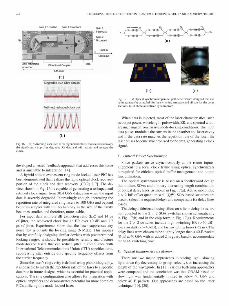
Fig. 16. (a) Si/InP ring laser used as 3R regenerative burst mode clock recovery(b) significantly improves degraded RZ data and will retimes and reshape theclock.
developed a nested feedback approach that addresses this issueand is amenable to integration [14].
A hybrid silicon evanescent ring mode-locked laser PIC hasbeen demonstrated that realizes the rapid optical clock recoveryportion of the clock and data recovery (CDR) [17]. The de-vice, shown in Fig. 16, is capable of generating a reshaped andretimed clock signal from 30.4 Gb/s data, even when the inputdata is severely degraded. Interestingly enough, increasing therepetition rate of integrated ring lasers to 100 GHz and beyondbecomes simpler with PIC technology as the size of the cavitybecomes smaller, and therefore, more stable.
For input data with 3.8 dB extinction ratio (ER) and 14 psof jitter, the recovered clock has an ER over 10 dB and 1.7ps of jitter. Experiments show that the laser suppresses anynoise that is outside the locking range (6 MHz). This impliesthat by carefully designing similar devices with predeterminedlocking ranges, it should be possible to reliably manufacturemode-locked lasers that can reduce jitter in compliance withInternational Telecommunications Union (ITU) specifications,suppressing jitter outside only specific frequency offsets fromthe carrier frequency.
Since the laser’s ring cavity is defined using photolithography,it is possible to match the repetition rate of the laser to a specificdata rate in future designs, which is essential for practical appli-cations. The ring configuration also allows for integration withoptical amplifiers and demonstrates potential for more complexPICs utilizing this mode-locked laser.
Fig. 17. (a) Optical synchronizer parallel path feedforward designed that canbe integrated (b) using InP for the switching structure and silicon for the delaysections. (c) It shows a realized synchronizer.
When data is injected, most of the laser characteristics, suchas output power, wavelength, pulsewidth, ER, and spectral widthare unchanged from passive mode-locking conditions. The inputdata pulses modulate the carriers in the absorber and laser cavityand if the data rate matches the repetition rate of the laser, thelaser pulses become synchronized to the data, generating a clocksignal.
C. Optical Packet Synchronizer
Since packets arrive asynchronously at the router inputs,alignment to a local clock frame using optical synchronizersis required for efficient optical buffer management and outputlink utilization.
The optical synchronizer is based on a feedforward designthat utilizes SOAs and a binary increasing length combinationof optical delay lines, as shown in Fig. 17(a). Active monolithic2 × 2 InP offset quantum-well (QW) SOA-based switches areused to select the required delays and compensate for delay lineslosses.
The delays, fabricated using silica-on-silicon delay lines, arebutt coupled to the 2 × 2 SOA switches shown schematicallyin Fig. 17(b) and in the chip form in Fig. 17(c). Requirementsfor the 2 × 2 switches include high switching ER (>40 dB),low crosstalk (<−40 dB), and fast switching times (<2 ns). Thedelay lines were chosen to be slightly longer than a 40-B packet(8 ns) at 40 Gb/s with an added 2 ns guard band to accommodatethe SOA switching time.
D. Optical Random Access Memory
There are two major approaches to storing light: slowinglight down (by decreasing its group velocity), or increasing thelength of the waveguide. In [18], various buffering approacheswere compared and the conclusion was that ORAM based onslow light was fundamentally limited to below 40 Gb/s andbelow 40 B packets. Our approaches are based on the lattertechnique [19], [20].

BLUMENTHAL et al.: INTEGRATED PHOTONICS FOR LOW-POWER PACKET NETWORKING 465
Fig. 18. InP 2 × 2 switch butt coupled to a silica delay line.
Fig. 19. Packet recovery for five recirculations shows up to 98% packet re-covery.
One PIC design, we have implemented a 2 × 2 switch on InPbutt coupled to a silica delay line, as shown in Fig. 18. Dependingon the bias condition of the SOAs, the signal can be routed fromthe ‘‘in’’ port to the ‘‘out’’ port either with or without delay.The delay was a 2 m (12.8 ns) long waveguide that at 40 Gb/sprovides 40 B of memory. Fig. 19 shows packet recovery againstreceived power for this device. A packet recovery rate of 98%was achieved after five circulations.
Decreasing the delay loss, the loss between passive and activeregions and regeneration (2R or 3R) are all approaches that canbe used to increase the buffer hold time. While the propagationloss of the silica waveguide is very low (<0.04 dB/cm) and theER of the InP switch is high (>40 dB), the butt couple canlead to reflections and the two chips have to be packaged. Anintegrated solution is required.
To address the loss-coupling issue between the active andpassive sections, an integrated buffer was fabricated on the hy-brid silicon platform [15]. Similar to the aforementioned design,a 2 × 2 switch is used to route a signal from the input to theoutput either with or without delay. Because of higher propaga-tion losses (∼2 dB/cm) compared to the silica-on-silicon, onlydelays of 7.6 cm (1.1 ns) were realized [2], which is more usefulfor packet synchronization than for memory. Fig. 20 shows theintegrated buffer storing a packet for 1.1 ns.
For the earlier platform, a major part of the propagation lossin the integrated buffer is introduced in the definition of theamplifiers (III–V processing). To address this issue, proper pas-sivation is needed to realize longer delay lines.
The latest generation of LASOR optical buffers in the hybridsilicon platform with a modification that the delay line (1.1 m) isprotected by SiO2 and SiN passivation layers to protect the delayline during the III–V processing. In addition, 2R regenerators forreamplification and reshaping have been integrated to amplify
Fig. 20. Optically buffered packet (a) with no delay (b) and 1.1 ns of delay.
Fig. 21. Integrated buffer with 2R regenerators on an silicon-on-insulatorsubstrate. A total of three buffers having 1.1 m of delay each are shown. Inaddition, various test structures and shorter buffers are on these chips.
and filter the signal. A photograph of the first fabricated chip isshown in Fig. 21.
E. Optical Wavelength Converters
Optical wavelength converters are used in LASOR for packetforwarding and are one of the two basic building blocks forthe switching fabric in addition to an AWGR. PIC realizationshave demonstrated wide tunable laser function, fast wavelengthswitching, and wavelength conversion without any electrical sig-nal conditioning at data rates of 40 Gb/s. In the LASOR project,we have developed, demonstrated, and incorporated into the fi-nal router test bed two types of devices: concurrent absorptionand modulation devices (such as Mach–Zehnder interferomet-ric (MZI)-SOA wavelength converters), and separate absorptionand modulation devices (such as a photocurrent driven exter-nally modulated laser architecture). This level of integrationsignificantly improves the performance, mainly through inser-tion loss reduction between the components, which translatesinto lower chip bias needs, and thus, lower thermal dissipation.
The overall power consumption for both device types wasdominated by the need for devices cooling, and more than half

466 IEEE JOURNAL OF SELECTED TOPICS IN QUANTUM ELECTRONICS, VOL. 17, NO. 2, MARCH/APRIL 2011
Fig. 22. Folded and unfolded versions of 40 Gb/s fast widely tunable CAMdifferential pulse MZI-SOA wavelength converters.
of the total power (2–2.5 W) was used up by the thermoelectriccooler.
Improvements that can be made to make these devices morepower efficient have to do with reduction of insertion losses,reduction of on-chip losses, and possible optimization of thechip integration platform, to allow for hotter operation of thedevices without performance degradation (which would reducethe need for cooling).
1) Concurrent Absorption and Modulation Wavelength Con-verters: In these device types, the interaction of photons andelectrons happens in adjacent waveguides, where the opticalmode overlaps the optical confinement and gain modulationregion at the same time (as in an SOA), and the wavelength con-version function is performed through nonlinear behavior in theSOA between the optical mode and the carrier population. Thisinteraction affects both phases and power levels of the signals,which is converted into an amplitude response through a use ofan interferometer. In LASOR program, we have demonstratedfive generations of tunable CAM wavelength converters operat-ing at 40 Gb/s, with the goal of improving their efficiency, andreducing the footprint.
Two implementations are shown in Fig. 22. Both designsare based on a differentially driven SOA-based MZI. A foldedcompact version of the device (top, 2.9 mm × 0.8 mm), anda more advanced design in terms of ability to independentlycontrol the phase and amplitude (bottom, 6.3 mm × 0.6 mm)are shown. The power dissipation on chip was dominated bythe nonlinear SOAs in the branches of the MZ (∼1.2 W). Thepower consumption did scale with bit rate, since higher SOAbias currents were needed at 40 Gb/s to speed up the responseof the carriers (0.8 W at 10 Gb/s and 1.2 W at 40 Gb/s).
2) Photocurrent-Driven Wavelength Converters: This typeof fast widely tunable wavelength converter operates by detect-ing the optical input using a preamplified photodiode. The pho-todiode electrode is shared with an optical modulator electrode,which is adjacent to the widely tunable laser, as shown in Fig. 23.Five different generations of these devices were explored, withperformance continually improving, and with maximum datarate reaching 40 Gb/s return to zero (RZ), after implementationof low capacitance, traveling wave electrodes.
Constant bias set-point operation of these devices was demon-strated across the data rates of 2.5 to 40 Gb/s, implying thepossibility of constant power consumption. However, it is pos-sible to optimize the biasing conditions for lower bit rates, andthus, reduce the consumption in this region of operation. An-
Fig. 23. SAM version of the monolithic fast widely tunable 40 Gb/s wave-length converter.
Fig. 24. Differential 40 Gb/s PFC with integrated optical label rewrite (upper),mounted chip on carrier (lower left) and packaged (lower right).
other advantage of this approach is that it does not use largeMZI-SOAs, which improves this chip’s efficiency significantly.Besides common improvements already discussed, these devicetypes would benefit from more optimized photodetectors (PDs)and modulators. We are now seeing much lower waveguidelosses in both the deeply etched structures as well as the QW in-termixing (QWI) structures, and we have more ideas, which themodeling indicates should get us to significantly better devices
F. Packet Forwarding Chip
CAM and SAM wavelength converters are used as a buildingblock for the PFCs of the optical switching fabric. The PFC addsto the differential tunable wavelength converter, the function oflabel modulation is added to the tunable wavelength converterplatforms. By using small modifications to the wavelength con-verter platforms, higher level of integration was achieved withadditional power saving. The PFCs illustrates the benefits ofintegrated photonics, through all the functions it provides: lightsplitting and amplification, new tunable wavelength generation,label erase function, label rewrite function, and payload wave-length conversion, all at 40 Gb/s line rate, and with less than 6 W(see Fig. 24). Two of the most important features of monolithicintegration are stability of phase sensitive delays and preserva-tion of photons by reducing losses normally required movingonto and off of several photonic chips.
G. Monolithic Tunable Optical Router
The MOTOR chip was the next step in evolution of mov-ing the LASOR switching fabric onto a single chip, furtherimproving performance, footprint, and power consumption. Im-proved energy efficiency is achieved by scaling the number of

BLUMENTHAL et al.: INTEGRATED PHOTONICS FOR LOW-POWER PACKET NETWORKING 467
Fig. 25. (a) Diagram of the MOTOR PIC illustrating eight input full function-ing PFCs connected to a low loss 8 × 8 AWGR. (b) Details of the individualPFCs. (c) Photomicrograph of the device.
photonic elements in a given chip. These large-scale PICs re-place many of the high-loss fiber-to-fiber connections betweenoptical components with low-loss waveguide transitions, reduc-ing the amount of power required for functions like signal am-plification to compensate for optical losses. For a function withcomplexity of that of the optical switching fabric, monolithicintegration has fairly significant impact.
We demonstrated integration of the elements within the dot-ted line in Fig. 10. The chip is called a MOTOR chip. The firstgeneration consisted of an array of eight 40 Gb/s wavelengthconverters and a passive AWGR. The device is one of the mostfunctionally complex InP photonic ICs ever reported, with morethan 200 integrated elements in a single chip, including multi-ple SOAs, a widely tunable sampled grating distributed Braggreflector (SG-DBR) laser, a passive differential delay line, vari-able optical attenuators, an AWGR, and phase shifters. Single-channel 40 Gb/s wavelength conversion and channel switchingrequired less than 2 W drive power and showed a power penaltyas low as 4.5 dB with a 231−1 pseudorandom binary sequencedata signal. MOTOR chip was part of the final technology demo,whose goal was to prove the extent of integration possible inthe router optical switch fabric. Therefore, the MOTOR chipconsisted of eight CAM PFC chips, integrated with an AWGR,forming an 8 × 8 optical switch fabric with total capacity of640 Gb/s and less than 50 W power consumption. At the time ofthe demonstration, this was one of the most complex PIC chipsdesigned to date (see Fig. 25).
VII. POWER AND BIT-SWITCHING ANALYSIS
The power consumed by the synchronizers and buffers weremeasured. For the top port, the power consumed by the synchro-nizer and buffer was 8.2 and 7.7 W, respectively. It is important
Fig. 26. OPS estimated power consumption breakdown of the total measuredpower consumption of 7.5 W.
Fig. 27. ORAM estimated power consumption breakdown of the total mea-sured power consumption of 7.7 W.
Fig. 28. PFC estimated power consumption breakdown of the total measuredpower consumption of 5.6 W.
to note that the calculations include the power needed to drivethe photonic devices as well as the power required to regulatethe temperature of each device. Photonics are highly tempera-ture dependent, therefore, temperature controllers are requiredfor proper operation. Furthermore, the photonic devices requireelectronic drivers to make the devices operational, so the powerconsumed in the drivers must go hand in hand with the powerconsumed in the optics. In order to further investigate, wherethe majority of power is consumed in the optical technologies,power estimates were calculated for the synchronizer and buffer.Packaged components were used that had the optical devices,electronic drivers, and temperature controllers powered by acommon power supply. The power consumption of the opticaldevices can be estimated assuming that the power consumed wasat maximum biasing of the SOAs, and the rest was consumedby electronic power dissipation and temperature control.
The results for the estimated breakdown of power consumedin the OPS, optical buffer, and PFC are shown in Figs. 26–28.

468 IEEE JOURNAL OF SELECTED TOPICS IN QUANTUM ELECTRONICS, VOL. 17, NO. 2, MARCH/APRIL 2011
A majority of the power is not consumed in the photonics, butrather in the electronic drivers and temperature controllers. Allof the photonic devices required SOAs for switching as well asto compensate for losses due to coupling, splitting, and propa-gation. If these losses can be reduced, then fewer and smallerSOAs can be used, which would reduce power. Addition-ally, more efficient SOA technology will further reduce powerconsumption. It should be noted that in the LASOR experiment,the electronic drivers for operating photonic devices were notoptimized for low-power operation.
Using state-of-the-art efficient electronic technologies will re-duce this measured component. Most photonic devices are cur-rently highly temperature dependent, therefore, temperature reg-ulation is required, which consumes the majority of power. If al-ternative means of temperature control that draw less power areimplemented or temperature-independent photonics are used,then the power consumed by the photonic devices can be re-duced drastically. It should be noted that although the use ofsynchronous buffers increases total power consumption com-pared to architectures that do not implement synchronization,overall control logic complexity is reduced that may reduceelectronic power consumption.
A rough calculation of the switching energy per bit for theLASOR system demonstration technology can be estimated bythe 110 W required to route 640 Gb/s or approximately 0.2nJ/bit (see Fig. 29). It is important to note this switching energyis achieved with first generation PICs and nonpower optimizedsupport electronics. Compared to the 3 nJ/bit switching energyfor today’s state-of-the-art router, the initial LASOR work showspotential for orders of magnitude improvement. It is importantto emphasize that the LASOR technologies are used as a proof ofprinciple and first-order analysis for power and energy and strictconclusions should not be drawn from these numbers, rather thepotential for trends by architecting new packet systems thatcombine PIC and electronic technologies.
VIII. SUMMARY AND CONCLUSION
In this paper, we have reviewed the role communications in-terconnects and networks play in the future contribution to theglobal carbon footprint, especially in data center and cloud-computing applications, which are expected to grow exponen-tially in traffic. We have also described the potential powerconsumption savings by integrating photonic technology intosystem architecture designs along with electronics technology.Key to maximizing the benefits of photonics technology is pho-tonics integration. In the context of an example packet routingsystem, the DARPA/MTO funded LASOR project, we have re-viewed the key PIC functions that have been realized and thepower contributions of these PIC technologies as more and morefunctions are integrated onto a single chip.
We have also quantified, through measurements, the powerconsumed by the photonics in performing their intended func-tion, the electronics required to bias the photonics, processingelectronics, and required cooling technology. In moving theoptical forwarding, buffering and other data plane functions tophotonics, the dominant contributions to power in packet routing
Fig. 29. Power consumption breakdown for the (a) arbiter, (b) line card, and(c) total power consumption for a two line card router.
have moved from the forwarding plane to the packet-processingplane.
There is still much room (potentially greater than 10×) forimprovement in the forwarding plane in the PIC technology andsupporting electronics, however, moving forward the focus willmost likely need to be on investigating photonic technologiesthat can impact the power consumption of the packet forwardingprocessing plane and in reducing cooling requirements in thedata forwarding plane as well as higher levels of monolithicintegration.
In the future, as the bit rates increase to 100 Gb/s and beyond,and coherent transmission technologies are employed, LASORtype technologies will need to scale to these new rates and beadapted to new modulation formats. There is also the poten-tial for the Internet to utilize packet sizes greater than 1500B (e.g., 5000 B super packets), and all the LASOR technolo-gies will work as the packet size increases. The major issue

BLUMENTHAL et al.: INTEGRATED PHOTONICS FOR LOW-POWER PACKET NETWORKING 469
will be with optical buffering that will require larger storagedelays with lower loss waveguides and regenerative buffers.Work is underway to design, fabricate, and test these new LA-SOR technologies and reports of progress will appear in futurepublications.
REFERENCES
[1] M. K. Patterson, D. G Costello, P. F. Grimm, and M. Loef-fler. (2005), “Data center TCO: A comparison of high-densityand low-density spaces,” Intel White Paper. [Online]. Available:www.intel.com/technology/eep/datacenter.pdf.
[2] D. J. Blumenthal, “Overview of the LASOR project,” presented at theWorkshop Opt. Packet Switching Opt. Burst Switching, Yokohama, Japan,Jul. 12, 2004 (Invited).
[3] D. J. Blumenthal and M. Masanovic, “LASOR: Label switched opticalrouter and photonic integration,” presented at the Eur. Conf. Opt. Com-mun., Glasgow, Scotland, U.K., Sep. 26–30, 2005 (Invited).
[4] D. J. Blumenthal, “Architecture and integration technologies for LASOR:A label switched optical router,” presented at the OSA Annu. Meeting,Rochester, NY, Oct. 9–12, 2006 (Invited).
[5] J. S. Barton, M. L. Masanovic, M. M. Dummer, A. Tauke-Pedretti, E.F. Burmeister, B. R. Koch, J. A. Summers, L. A. Coldren, J. E. Bowers,and D. J. Blumenthal, “Recent progress on LASOR optical router andrelated integrated technologies,” presented at the Int. Topical Mtg. Photon.Switching, Sapporo, Japan, Aug. 4–7, 2008 (Invited).
[6] M. Enachescu, Y. Ganjali, A. Goel, N. McKeown, and T. Roughgarden,“Routers with very small buffers,” in Proc. IEEE INFOCOM, Barcelona,Spain, Apr. 2006, pp. 1–11.
[7] N. Beheshti, Y. Ganjali, R. Rajaduray, D. Blumenthal, and N. McKe-own, “Buffer sizing in all-optical packet switches,” presented at theOFC/NFOEC, Anaheim, CA, Mar. 2006.
[8] N. Beheshti, Y. Ganjali, M. Ghobadi, N. McKeown, and G. Salmon,“Experimental study of router buffer sizing,” in Proc. Internet Meas.Conf., Vouliagmeni, Greece, Oct.2008, pp. 197–210.
[9] M. L. Masanovic, E. Burmeister, M. M. Dummer, B. Koch, S. C. Nicholes,J. S. Barton, B. Jevremovic, K. Nguyen, V. Lal, J. E. Bowers, L. A. Coldren,and D. J. Blumenthal, “Advanced photonic integrated technologies foroptical routing and switching,” presented at the 2009 SPIE/Photon. West,San Jose, CA, to be published.
[10] R. Nagarajan, M. Kato, J. Pleumeekers, P. Evans, D. Lambert, A. Chen,V. Dominic, A. Mathur, P. Chavarkar, M. Missey, A. Dentai, S. Hurtt,J. Back, R. Muthiah, S. Murthy, R. Salvatore, C. Joyner, J. Rossi, R.Schneider, M. Ziari, H.-S. Tsai, J. Bostak, M. Kauffman, S. Pennypacker,T. Butrie, M. Reffle, D. Mehuys, M. Mitchell, A. Nilsson, S. Grubb, F.Kish, and D. Welch, “Large-scale photonic integrated circuits for longhaul transmission and switching,” J. Opt. Net., vol. 6, pp. 102–111, Feb.2007.
[11] P. Koh, Y. Akulova, and G. Fish, “Chirp-controlled EA-modulator/SOAwidely-tunable laser transmitter,” presented at 2005 Opt. Fiber Commun.Conf., Anaheim, CA, Mar. 6–11, 2005.
[12] Z. Hu, R. Doshi, H.-F. Chou, H. P. Poulsen, D. Wolfson, J. E. Bowers,and D. J. Blumenthal, “Optical label swapping using payload envelopedetection circuits,” IEEE Photon. Tech. Lett., vol. 17, no. 7, pp. 1537–1539, Jul. 2005.
[13] B. R. Koch, Z. Hu, J. E. Bowers, and D. J. Blumenthal, “All-opticalpayload envelope detection for variable length 40 Gbps optically labeledpackets,” IEEE Photon. Tech. Lett., vol. 18, no. 17, pp. 1846–1848, Sep.2006.
[14] H. N. Poulsen, D. Wolfson, S. Rangarajan, and D. J. Blumenthal, “Burstmode 10 Gbps optical header recovery and lookup processing for asyn-chronous variable-length 40 Gbps optical packet switching,” presented atthe Opt. Fiber Commun. Conf., Anaheim, CA, Mar. 5–10, 2006.
[15] A. W. Fang, R. Jones, H. Park, O. Cohen, O. Raday, M. J. Paniccia, and J.E. Bowers, “Integrated AlGaInAs-silicon evanescent race track laser andphotodetector,” Opt. Exp., vol. 15, pp. 2315–2322, 2007.
[16] Z. Hu, H.-F. Chou, K. Nishimura, M. Usami, J. E. Bowers, and D. J.Blumenthal, “Optical clock recovery circuits using traveling-wave elec-troabsorption modulator-based ring oscillators for 3R regeneration,” IEEEJ. Sel. Topics Quantum Electron., vol. 11, no. 2, pp. 329–337, Mar./Apr.2005.
[17] B. R. Koch, A. W. Fang, H. N. Poulsen, H. Park, D. J. Blumenthal, J.E. Bowers, R. Jones, M. J. Paniccia, and O. Cohen, “All-optical clockrecovery with retiming and reshaping using a silicon evanescent mode
locked ring laser,” in Proc. Opt. Fiber Commun. Conf., San Diego, CA,Feb. 24–28, 2008, pp. 1–3, (Invited Paper OMN1).
[18] M. J. R. Heck, G. Kurczveil, E. F. Burmeister, H. Park, J. P. Mack, D. J.Blumenthal, and J. E. Bowers, “Integrated recirculating optical buffers,”presented at the SPIE Photon. West 2010, CA, 2010.
[19] E. F. Burmeister, D. J. Blumenthal, and J. E. Bowers, “Optical bufferingfor next-generation routers,” presented at the Opto-Electron. Commun.Conf., Kaohsiung, Taiwan, Jul. 3–7, 2006, (Invited).
[20] E. F. Burmeister, J. P. Mack, H. N. Poulsen, M. L. Masanovic, B. Stamenic,D. J. Blumenthal, and J. E. Bowers, “Photonic chip recirculating bufferfor optical packet switching,” Opt. Exp., vol. 17, no. 8, pp. 6629–6635,Apr. 2009.
[21] M. L. Masanovic, V. Lal, J. A. Summers, J. S. Barton, E. J. Skogen, L.G. Rau, L. A. Coldren, and D. J. Blumenthal, “Widely tunable mono-lithically integrated all-optical wavelength converters in InP,” J. Lightw.Technol., vol. 23, no. 3, pp. 1350–1362, Mar. 2005.
[22] V. Lal, M. L. Masanovic, J. A. Summers, G. Fish, and D. J. Blumenthal,“Monolithic wavelength converters for high-speed packet-switched opti-cal networks,” IEEE J. Sel. Topics Quantum Electron., vol. 13, no. 1,pp. 49–57, Jan./Feb. 2007.
[23] M. M. Dummer, J. Klamkin, A. Tauke-Pedretti, K. N. Nguyen, and L.A. Coldren, “Field-modulated packet forwarding chips for label-switchedoptical routing,” in Proc. Opt. Fiber Commun. Conf.—Incudes Post Dead-line Papers, OFC 2009, Mar. 22–26,, pp. 1–3.
[24] J. A. Summers, V. Lal, M. L. Masanovic, L. A. Coldren, and D. J. Blumen-thal, “Widely-Tunable all-optical wavelength converter monolithically in-tegrated with a total internal reflection corner mirror delay line for 40 GbpsRZ operation,” presented at the Integr. Photon. Res. Appl., San Diego,CA, Apr. 11–13, 2005.
[25] W. B. Zhao, M. L. Masanovic, V. Lal, D. Wolfson, G. Fish, and D. J. Blu-menthal, “Widely tunable monolithically integrated 40 Gbit/s wavelengthconverter with label modulation function,” Electron. Lett., vol. 42, no. 21,pp. 1241–1243, Oct. 12, 2006.
[26] M. N. Sysak, J. W. Raring, M. Dummer, H. N. Poulsen, D. J. Blumenthal,and L. A. Coldren, “Analysis of digital system performance in EAM-based photocurrent driven wavelength converter,” IEEE Photon. Tech.Lett., vol. 19, no. 4, pp. 215–217, Feb. 2007.
[27] A. Tauke-Pedretti, M. M. Dummer, M. N. Sysak, J. S. Barton, J. Klamkin,J. W. Raring, and L. A. Coldren, “Separate absorption and modulationmach-zehnder wavelength converter,” J. Lightw. Technol., vol. 26, no. 1,pp. 91–98, Jan. 2008.
[28] V. Lal, M. Masanovic, D. Wolfson, G. Fish, and D. Blumenthal, “Mono-lithic widely tunable packet forwarding chip in InP for all-optical labelswitching,” presented at the Integr. Photon. Res. Appl. Topical Meeting,Uncasville, CT, Apr. 24–26, 2006 (Invited).
[29] S. C. Nicholes, M. L. Masanovic, B. Jevremovic, E. Lively, L. A. Coldren,and D. J. Blumenthal, “An 8×8 InP monolithic tunable optical router(MOTOR) packet forwarding chip,” J. Lightw. Technol., vol. 4, pp. 641–650, Feb. 2009.
Daniel J. Blumenthal (S’91–M’93–SM’97–F’03)received the B.S.E.E. degree from the University ofRochester, Rochester, NY, in 1981, the M.S.E.E. de-gree from Columbia University, New York, NY, in1988, and the Ph.D. degree from the University ofColorado, Boulder, in 1993.
He is currently a Professor in the Department ofElectrical and Computer Engineering, University ofCalifornia, Santa Barbara (UCSB). He is also the Di-rector of the Terabit Optical Ethernet Center and theLASOR project at UCSB, a project funded by the
DARPA/MTO Data in the Optical Domain Network program. He is currentlyon the Board of Directors for National LambdaRail and on the Internet2 Archi-tecture Advisory Council. He is a Co-Founder of Calient Networks, and morerecently, Packet Photonics, LLC. He has authored or coauthored more than 350papers in various areas. His research interests include optical communications,photonic packet switching and all-optical networks, all-optical wavelength con-version and regeneration, ultrafast communications, InP photonic integratedcircuits, and nanophotonic device technologies.
Dr. Blumenthal is a Fellow of the IEEE Photonics and CommunicationsSocieties and a Fellow of the Optical Society of America. He is the recipient ofa 1999 Presidential Early Career Award for Scientists and Engineers from theWhite House, a 1994 National Science Foundation Young Investigator Award,and a 1997 Office of Naval Research Young Investigator Program Award.

470 IEEE JOURNAL OF SELECTED TOPICS IN QUANTUM ELECTRONICS, VOL. 17, NO. 2, MARCH/APRIL 2011
John Barton, photograph and biography not available at the time of publication.
Neda Beheshti received the B.S. degree from SharifUniversity of Technology, Tehran, Iran, the M.S. de-gree from Northeastern University, Boston, MA, andthe Ph.D. degree from Stanford University, Palo Alto,CA, all in electrical engineering.
She joined Ericsson Research Lab, San Jose CA,in 2009. Her current research interests include routerand switch architectures, wireless networking, andthe architecture of the future Internet.
Dr. Beheshti was the recipient of the Best PaperAward of the Internet Measurement Conference 2008
and the Second Best Demo Award of Annual Meeting of the Special InterestGroup on Data Communication (SIGCOMM) 2008 for her work on router buffersizing.
John E. Bowers (F’93) received the M.S. and Ph.D.degrees from Stanford University, Palo Alto, CA.
He was with AT&T Bell Laboratories and Honey-well. He holds the Fred Kavli Chair in nanotechnol-ogy and is currently the Director of the Institute forEnergy Efficiency and a Professor in the Departmentof Electrical and Computer Engineering, Universityof California, Santa Barbara. His research interestsinclude silicon photonic integrated circuits for thenext generation of coherent optical systems.
Dr. Bowers is a member of the National Academyof Engineering, and a Fellow of the Optical Society of America (OSA) and theAmerican Physical Society. He is also the recipient of the OSA Holonyak Prize,the IEEE Lasers and Electrooptics Society (LEOS), (now the IEEE PhotonicsSociety) William Streifer Award, and the South Coast Business and TechnologyEntrepreneur of the Year Award. He was the corecipient of the Annual Creativ-ity in Electronics Award for Most Promising Technology for the hybrid siliconlaser in 2007.
Emily Burmeister received the B.S. degree in en-gineering physics from the University of Michigan,Ann Arbor, MI, in May 2002, and the Ph.D. degreefrom the University of California, Santa Barbara, inMay 2008. Her thesis was titled as Integrated OpticalBuffers for Packet-Switched Networks.
She is currently with Ciena Corporation,Linthicum, MD.
Larry A. Coldren (S’67–M’72–SM’77–F’82) re-ceived the Ph.D. degree in Electrical Engineeringfrom Stanford University, CA, in 1972.
He is the Fred Kavli Professor of Optoelectronicsand Sensors and Acting Richard A. Auhll Dean ofEngineering at the University of California (UCSB),Santa Barbara. he joined UCSB in 1984, where henow holds appointments in Materials and Electricaland Computer Engineering. In 1990, he cofoundedOptical Concepts, later acquired as Gore Photonics,to develop novel VCSEL technology, and in 1998, he
cofounded Agility Communications, later acquired by JDSU, to develop widely-tunable integrated transmitters. For 13 years, he was at Bell Laboratories, wherehe was initially involved in wave-guided surface-acoustic-wave signal process-ing devices and coupled-resonator filters. He later developed tunable coupled-cavity lasers using novel reactive-ion etching technology that he created for thethen new InP-based materials. At UCSB, he continued to be engaged in multiple-section tunable lasers, and in 1988 invented the widely tunable multi-elementmirror concept, which is now used in some JDSU products. Near this same timeperiod, he also made seminal contributions to efficient vertical-cavity surface-
emitting laser (VCSEL) designs that continue to be implemented in practicaldevices to this day. More recently, his group has developed high-performanceInP-based photonic integrated circuits as well as high-speed VCSELs, and theycontinue to advance the underlying materials growth and fabrication technolo-gies. He has authored or coauthored over a thousand journal and conferencepapers, 7 book chapters, 1 textbook, and has been issued 63 patents. He haspresented dozens of invited and plenary talks at major conferences.
Dr. Coldren is a Fellow of the Optical Society of America and Institutionof Electrical Engineers, a recipient of the 2004 John Tyndall and 2009 AronKressel Awards, and a member of the National Academy of Engineering.
Matt Dummer, photograph and biography not available at the time of publi-cation.
Garry Epps has been with Cisco Systems since 1992,where he is now a Distinguished Engineer. Duringhis career at Cisco he has helped pioneer many firstsin the routing industry including ATM and packetover synchronous optical networking (POS) interfacetechnologies. He was one of the lead architects of thewidely deployed Cisco 12000 series (GSR) routerfamily, which was the industry’s first carrier-grade IProuter. He was the architect of several generations ofapplication-specified integrated circuits used for IPpacket forwarding. He continues in a leading role in
architecting the next-generation high-end routing platforms within Cisco. Heactively participates in research relating to system power reduction and opticalpacket switching.
Alexander Fang (S’04–M’09) received the B.S. de-gree in electrical engineering with minors in physicsand mathematics from San Jose State University, SanJose, CA, in 2003, and the M.S. and Ph.D. degrees inelectrical engineering from the University of Califor-nia, Santa Barbara, in 2005 and 2008, respectively.His Ph.D. dissertation focused on “silicon evanescentlasers.”
He is the CEO and co-founder of Aurrion, SantaBarbara, CA. He was also with Lawrence LivermoreNational Laboratory and Intel Prior to founding Au-
rrion. Alex is a leader in the field of silicon photonics and photonic integratedcircuits. He is the author or coauthor of more than 70 papers in his field and hasfiled 6 patents.
Dr. Fang has won a number of awards for the technology he developed to-gether with Prof. Bowers and colleagues.
Yashar Ganjali (S’03–M’07) received the B.Sc. de-gree in computer engineering from Sharif Universityof Technology, Tehran, Iran, in 1999, the M.Sc. de-gree in computer science from the University of Wa-terloo, Waterloo, ON, in 2001, and the Ph.D. degreein electrical engineering from Stanford University,Palo Alto, CA, in 2006.
He is currently a Faculty Member in ComputerScience Department, University of Toronto, Toronto,ON. His research interests include packet-switchingarchitectures/algorithms, network protocols and mea-
surement, network management, and online social networks.Dr. Ganjali was the recipient of several awards for his research including Best
Paper Award in Internet Measurement Conference 2008, Best Paper Runner upin Conference on Information Communications Marketplace (INFOCOMM)2003, Best Demo Runner up in Annual Meeting of the Special Interest Groupon Data Communication (SIGCOMM) 2008, Best Demo in NetFPGA Work-shop 2009, Leaders Opportunity Fund from Canada Foundation for Innovation,and Cisco Research Award.

BLUMENTHAL et al.: INTEGRATED PHOTONICS FOR LOW-POWER PACKET NETWORKING 471
John Garcia, photograph and biography not available at the time of publication.
Brian Koch, photograph and biography not available at the time of publication.
Vikrant Lal, photograph and biography not available at the time of publication.
Erica Lively, photograph and biography not available at the time of publication.
John Mack, photograph and biography not available at the time of publication.
Milan Masanovic (S’98–M’04) received the Dipl.Ing. degree from the School of Electrical Engineer-ing, University of Belgrade, Belgrade, Yugoslavia,and the M.S. and Ph.D. degrees from the Univer-sity of California at Santa Barbara, Santa Barbara, in1998, 2000, and 2004, respectively, all in electricalengineering.
He is currently an Adjunct Assistant Professor atthe University of California at Santa Barbara, and aprincipal and a founder of Freedom Photonics LLC,a photonic integration company in Santa Barbara,
CA.He is the author or coauthor of more than 75 research papers. His currentresearch interests include InP photonic integration related to applications inpacket-switched optical networks.
Dr. Masanovic was the recipient numerous awards and fellowships, includingthe 2004 IEEE Lasers and Electro-Optics Society Graduate Student FellowshipAward and the 2003 Best Student Paper Award at the Indium Phosphide andRelated Materials Conference.
Nick McKeown received the B.E. degree from theUniversity of Leeds, Leeds, U.K., in 1986, and thePh.D. and M.S. degrees from the University of Cali-fornia, Berkeley, in 1995 and 1992, respectively.
He is currently a Professor of Electrical Engineer-ing and Computer Science, and the Faculty Directorof the Clean Slate Program at Stanford University,CA. From 1986 to 1989, he was with Hewlett-PackardLabs, Bristol, England. In 1995, he assisted architectCisco’s GSR 12000 router. In 1997, he cofoundedAbrizio, Inc., (acquired by PMC-Sierra), where he
was CTO. He was also the cofounder and CEO of Nemo (“Network Memory”),which is now a part of Cisco. His research interests include the architectureof the future Internet, and tools and platforms for networking teaching andresearch.
Dr. McKeown is the STMicroelectronics Faculty Scholar, the Robert NoyceFaculty Fellow, a Fellow of the Powell Foundation, the Alfred P. Sloan Foun-dation, the Royal Academy of Engineering (U.K.), and the Association forComputing Machinery (ACM). He is the recipient of a CAREER award fromthe National Science Foundation. In 2000, he received the IEEE Rice Award forthe best paper in communications theory. In 2005, he was awarded the BritishComputer Society Lovelace Medal, and in 2009 the IEEE Kobayashi Computerand Communications Award.
Kim Nguyen received the B.S. and M.Eng. degreesfrom the University of Louisville, Louisville, KY, in2005 and 2007, respectively. She is currently workingtoward the Ph.D. degree at the University of Califor-nia, Santa Barbara.
Her research interests include photonic integratedcircuits, advanced modulation formats, coherent op-tical receivers, and optical regenerators.
Steven C. Nicholes received the B.S. degree in chem-ical engineering from Brigham Young University,Provo, UT, in 2005, and the Ph.D. degree in materialsfrom the University of California, Santa Barbara in2009. His Ph.D. thesis focused on the design, growth,and fabrication of large-scale photonic integratedcircuits.
Since 2009, he has been with Aurrion, LLC,Santa Barbara, CA, where he is involved in siliconphotonics.
Hyundai Park, photograph and biography not available at the time ofpublication.
Biljana Stamenic received the Dipl. Ing. and theM.S. degrees in metallurgy of nonferrous metals fromthe School of Technology and Metallurgy Universityof Belgrade, Belgrade, Yugoslavia, in 1994 and 1999,respectively, all in metallurgy engineering. Her M.S.thesis focused on metallurgy of nonferrous metals.
From 1994 to 1999, she was a Research Assis-tant at the Institute for Technology of Nuclear andOther Mineral Row Materials, Belgrade. From 2002to 2006, she was a Device Fabrication Technician atDuPont Displays, Santa Barbara, CA. She is currently
a Senior Development Engineer at the University of California at Santa Barbara,where the majority responsibilities of her work include layout and prototypingof the advanced photonic integrated circuit chips and fabrication process devel-opment duties related to device fabrication.
Anna Tauke-Pedretti (S’02–M’08) received theB.S. degree in physics and electrical engineering fromthe University of Iowa, Iowa City, in 2001, and theM.S. and Ph.D. degrees in electrical and computerengineering from the University of California, SantaBarbara, in 2002 and 2007, respectively. Her Ph.D.dissertation focused on the design, fabrication, andtesting of InP-based photonic integrated circuits forhigh-speed wavelength conversion.
In 2008, she joined Sandia National Laboratories,Albuquerque, NM, as a senior member of technical
staff, where she continues to be involved in the development of novel photonicintegrated circuits. Her current research interests include optical injection lock-ing, high-speed modulators, and high-power integrated receivers.
Henrik Poulsen, photograph and biography not available at the time of publi-cation.
Matt Sysak, photograph and biography not available at the time of publication.