500ma fixed output cmos ldo - microchip...
TRANSCRIPT

2002 Microchip Technology Inc. DS21373B-page 1
TC1262
Features
• Very Low Dropout Voltage
• 500mA Output Current
• High Output Voltage Accuracy
• Standard or Custom Output Voltages
• Over Current and Over Temperature Protection
Applications
• Battery Operated Systems
• Portable Computers
• Medical Instruments
• Instrumentation
• Cellular/GSM/PHS Phones
• Linear Post-Regulators for SMPS
• Pagers
Device Selection Table
NOTE: xx indicates output voltages.
Available Output Voltages: 2.5, 2.8, 3.0, 3.3, 5.0.
Other output voltages are available. Please contact MicrochipTechnology Inc. for details.
Package Type
General Description
The TC1262 is a fixed output, high accuracy (typically±0.5%) CMOS low dropout regulator. Designed specif-ically for battery-operated systems, the TC1262’sCMOS construction eliminates wasted ground current,significantly extending battery life. Total supply currentis typically 80µA at full load (20 to 60 times lower thanin bipolar regulators).
TC1262 key features include ultra low noise operation,very low dropout voltage (typically 350mV at full load),and fast response to step changes in load.
The TC1262 incorporates both over temperature andover current protection. The TC1262 is stable with anoutput capacitor of only 1µF and has a maximumoutput current of 500mA. It is available in 3-PinSOT-223, 3-Pin TO-220 and 3-Pin DDPAK packages.
Typical Application
Part Number PackageJunction
Temp. Range
TC1262-xxVDB 3-Pin SOT-223 -40°C to +125°C
TC1262-xxVAB 3-Pin TO-220 -40°C to +125°C
TC1262-xxVEB 3-Pin DDPAK -40°C to +125°C
VIN
VIN
VOUT
GND
GN
D
VO
UT
Tab
is G
ND
Front View
Front View
1
1 2 3
3
2
Tab is GND
TC1262
TC1262
VIN
VO
UT
TC1262
3-Pin TO-220
Tab is GND
3-Pin SOT-223
3-Pin DDPAK
1 2 3
GN
D
TC1262
VIN VOUT
C11µF
GND
VOUTVIN +
500mA Fixed Output CMOS LDO
TC1262
DS21373B-page 2 2002 Microchip Technology Inc.
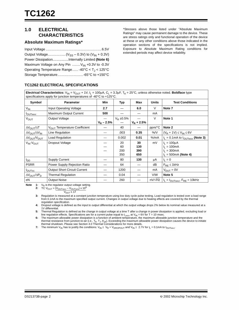
1.0 ELECTRICALCHARACTERISTICS
Absolute Maximum Ratings*
Input Voltage .........................................................6.5V
Output Voltage.................. (VSS – 0.3V) to (VIN + 0.3V)
Power Dissipation................Internally Limited (Note 6)Maximum Voltage on Any Pin ........VIN +0.3V to -0.3V
Operating Temperature Range...... -40°C < TJ < 125°C
Storage Temperature.......................... -65°C to +150°C
*Stresses above those listed under "Absolute MaximumRatings" may cause permanent damage to the device. Theseare stress ratings only and functional operation of the deviceat these or any other conditions above those indicated in theoperation sections of the specifications is not implied.Exposure to Absolute Maximum Rating conditions forextended periods may affect device reliability.
TC1262 ELECTRICAL SPECIFICATIONS
Electrical Characteristics: VIN = VOUT + 1V, IL = 100µA, CL = 3.3µF, TA = 25°C, unless otherwise noted. Boldface typespecifications apply for junction temperatures of -40°C to +125°C.
Symbol Parameter Min Typ Max Units Test Conditions
VIN Input Operating Voltage 2.7 — 6.0 V Note 7
IOUTMAX Maximum Output Current 500 — — mA
VOUT Output Voltage —VR – 2.5%
VR ±0.5%—
—VR + 2.5%
V Note 1
∆VOUT/∆T VOUT Temperature Coefficient — 40 — ppm/°C Note 2
∆VOUT/∆VIN Line Regulation — .003 0.35 %/V (VR + 1V) ≤ VIN ≤ 6V
∆VOUT/VOUT Load Regulation — 0.002 0.01 %/mA IL = 0.1mA to IOUTMAX (Note 3)
VIN-VOUT Dropout Voltage ———
2060200350
30130390650
mV IL = 100µAIL = 100mAIL = 300mAIL = 500mA (Note 4)
IDD Supply Current — 80 130 µA IL = 0
PSRR Power Supply Rejection Ratio — 64 — dB FRE ≤ 1kHz
IOUTSC Output Short Circuit Current — 1200 — mA VOUT = 0V
∆VOUT/∆PD Thermal Regulation — 0.04 — V/W Note 5
eN Output Noise — 260 — nV/√Hz IL = IOUTMAX, FRE = 10kHz
Note 1: VR is the regulator output voltage setting.2:
3: Regulation is measured at a constant junction temperature using low duty cycle pulse testing. Load regulation is tested over a load rangefrom 0.1mA to the maximum specified output current. Changes in output voltage due to heating effects are covered by the thermalregulation specification.
4: Dropout voltage is defined as the input to output differential at which the output voltage drops 2% below its nominal value measured at a1V differential.
5: Thermal Regulation is defined as the change in output voltage at a time T after a change in power dissipation is applied, excluding load orline regulation effects. Specifications are for a current pulse equal to ILMAX at VIN = 6V for T = 10 msec.
6: The maximum allowable power dissipation is a function of ambient temperature, the maximum allowable junction temperature and thethermal resistance from junction-to-air (i.e., TA, TJ, θJA). Exceeding the maximum allowable power dissipation causes the device to initiatethermal shutdown. Please see Section 4.0 Thermal Considerations for more details.
7: The minimum VIN has to justify the conditions: VIN ≥ VR + VDROPOUT and VIN ≥ 2.7V for IL = 0.1mA to IOUTMAX.
TC VOUT = (VOUTMAX – VOUTMIN) x 106
VOUT x ∆T
2002 Microchip Technology Inc. DS21373B-page 3
TC1262
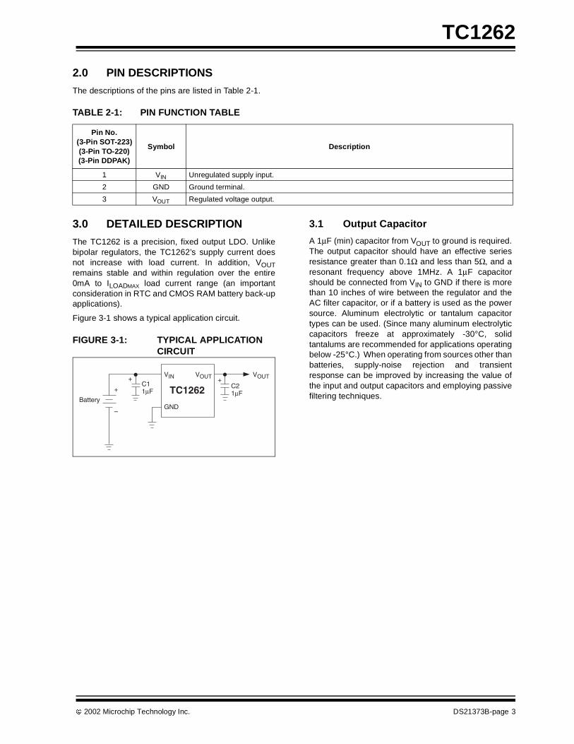
2.0 PIN DESCRIPTIONS
The descriptions of the pins are listed in Table 2-1.
TABLE 2-1: PIN FUNCTION TABLE
3.0 DETAILED DESCRIPTION
The TC1262 is a precision, fixed output LDO. Unlikebipolar regulators, the TC1262’s supply current doesnot increase with load current. In addition, VOUTremains stable and within regulation over the entire0mA to ILOADMAX load current range (an importantconsideration in RTC and CMOS RAM battery back-upapplications).
Figure 3-1 shows a typical application circuit.
FIGURE 3-1: TYPICAL APPLICATIONCIRCUIT
3.1 Output Capacitor
A 1µF (min) capacitor from VOUT to ground is required.The output capacitor should have an effective seriesresistance greater than 0.1Ω and less than 5Ω, and aresonant frequency above 1MHz. A 1µF capacitorshould be connected from VIN to GND if there is morethan 10 inches of wire between the regulator and theAC filter capacitor, or if a battery is used as the powersource. Aluminum electrolytic or tantalum capacitortypes can be used. (Since many aluminum electrolyticcapacitors freeze at approximately -30°C, solidtantalums are recommended for applications operatingbelow -25°C.) When operating from sources other thanbatteries, supply-noise rejection and transientresponse can be improved by increasing the value ofthe input and output capacitors and employing passivefiltering techniques.
Pin No.(3-Pin SOT-223)(3-Pin TO-220)(3-Pin DDPAK)
Symbol Description
1 VIN Unregulated supply input.
2 GND Ground terminal.
3 VOUT Regulated voltage output.
C11µF
BatteryTC1262
VIN VOUT
C21µF
GND
VOUT+
+
+
–
TC1262
DS21373B-page 4 2002 Microchip Technology Inc.
4.0 THERMAL CONSIDERATIONS
4.1 Thermal Shutdown
Integrated thermal protection circuitry shuts theregulator off when die temperature exceeds 160°C.The regulator remains off until the die temperaturedrops to approximately 150°C.
4.2 Power Dissipation
The amount of power the regulator dissipates isprimarily a function of input and output voltage, andoutput current. The following equation is used tocalculate worst case actual power dissipation:
EQUATION 4-1:
The maximum allowable power dissipation (Equation4-2) is a function of the maximum ambient temperature(TAMAX), the maximum allowable die temperature(TJMAX) and the thermal resistance from junction-to-air(θJA).
EQUATION 4-2:
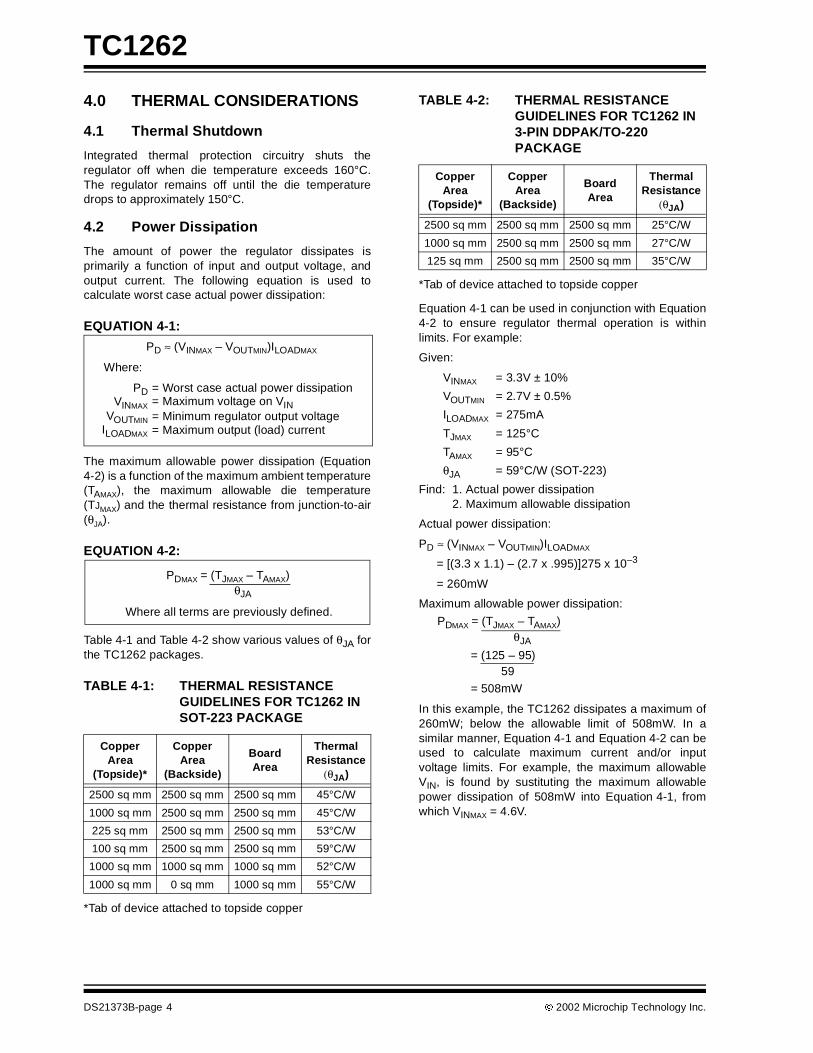
Table 4-1 and Table 4-2 show various values of θJA forthe TC1262 packages.
TABLE 4-1: THERMAL RESISTANCEGUIDELINES FOR TC1262 INSOT-223 PACKAGE
*Tab of device attached to topside copper
TABLE 4-2: THERMAL RESISTANCEGUIDELINES FOR TC1262 IN3-PIN DDPAK/TO-220PACKAGE
*Tab of device attached to topside copper
Equation 4-1 can be used in conjunction with Equation4-2 to ensure regulator thermal operation is withinlimits. For example:
Given:
VINMAX = 3.3V ± 10%
VOUTMIN = 2.7V ± 0.5%
ILOADMAX = 275mA
TJMAX = 125°C
TAMAX = 95°C
θJA = 59°C/W (SOT-223)
Find: 1. Actual power dissipation2. Maximum allowable dissipation
Actual power dissipation:
PD ≈ (VINMAX – VOUTMIN)ILOADMAX
= [(3.3 x 1.1) – (2.7 x .995)]275 x 10–3
= 260mW
Maximum allowable power dissipation:
In this example, the TC1262 dissipates a maximum of260mW; below the allowable limit of 508mW. In asimilar manner, Equation 4-1 and Equation 4-2 can beused to calculate maximum current and/or inputvoltage limits. For example, the maximum allowableVIN, is found by sustituting the maximum allowablepower dissipation of 508mW into Equation 4-1, fromwhich VINMAX = 4.6V.
CopperArea
(Topside)*
CopperArea
(Backside)
BoardArea
ThermalResistance
(θJA)
2500 sq mm 2500 sq mm 2500 sq mm 45°C/W
1000 sq mm 2500 sq mm 2500 sq mm 45°C/W
225 sq mm 2500 sq mm 2500 sq mm 53°C/W
100 sq mm 2500 sq mm 2500 sq mm 59°C/W
1000 sq mm 1000 sq mm 1000 sq mm 52°C/W
1000 sq mm 0 sq mm 1000 sq mm 55°C/W
Where:
PD ≈ (VINMAX – VOUTMIN)ILOADMAX
PDVINMAX
VOUTMINILOADMAX
= Worst case actual power dissipation
= Minimum regulator output voltage= Maximum output (load) current
= Maximum voltage on VIN
PDMAX = (TJMAX – TAMAX)θJA
Where all terms are previously defined.
CopperArea
(Topside)*
CopperArea
(Backside)
BoardArea
ThermalResistance
(θJA)
2500 sq mm 2500 sq mm 2500 sq mm 25°C/W
1000 sq mm 2500 sq mm 2500 sq mm 27°C/W
125 sq mm 2500 sq mm 2500 sq mm 35°C/W
PDMAX = (TJMAX – TAMAX)θJA
= (125 – 95)59
= 508mW

2002 Microchip Technology Inc. DS21373B-page 5
TC1262
5.0 TYPICAL CHARACTERISTICS
Note: The graphs and tables provided following this note are a statistical summary based on a limited number ofsamples and are provided for informational purposes only. The performance characteristics listed herein arenot tested or guaranteed. In some graphs or tables, the data presented may be outside the specifiedoperating range (e.g., outside specified power supply range) and therefore outside the warranted range.
Output Noise vs. Frequency
FREQUENCY (kHz)
NO
ISE
(µV
/√H
z)
10.0
1.0
0.01 0.01 1 10 100 1000
0.1
0.0
RLOAD = 50µΩCOUT = 1µF
0.020
0.018
0.016
0.012
0.010
0.008
0.006
0.004
0.002
0.000
0.014
TEMPERATURE (°C)
Line Regulation vs. Temperature
LIN
E R
EG
UL
AT
ION
(%
)
-40°C 0°C 25°C 70°C 85°C 125°C -40°C 0°C 25°C 70°C 85°C 125°C
0.0100
0.0090
0.0080
0.0070
0.0060
0.0050
0.0040
0.0030
0.0020
0.0010
0.0100
TEMPERATURE (°C)
Load Regulation vs. Temperature
LO
AD
RE
GU
LA
TIO
N (
%/m
A)
1mA to 500mA
1mA to 500mA
5V
2.5V
TEMPERATURE (°C)
I DD
(µA
)
150
135
120
105
90
75
60
45
30
15
0
IDD vs. Temperature
5V
-40°C 0°C 25°C 70°C 85°C 125°C 0 100 200 300 400 500
ILOAD (mA)
0 100 200 300 400 500
ILOAD (mA)
2.5V Dropout Voltage vs. ILOAD
DR
OP
OU
T V
OL
TA
GE
(V
)
2.5V
0.50
0.40
0.30
0.20
0.10
0.00
0.50
0.40
0.30
0.20
0.10
0.00
LOAD
DR
OP
OU
T V
OL
TA
GE
(V
)25°C
-40°C
-40°C
0°C
0°C
70°C
70°C85°C
1125°C
85°C
25°C
125°C
2.70
2.50
2.30
2.10
1.90
1.70
1.50-40°C 0°C 25°C 70°C 85°C 125°C
TEMPERATURE (°C)
2.5V VOUT vs. Temperature
IL = 0.1mA
IL A= 300mA
IIIL AA= 500mA
5.205.105.004.904.80
4.70
4.60
4.50
4.40
4.30
4.20
4.104.00
-40°C 0°C 25°C 70°C 85°C 125°C
TEMPERATURE (°C)
5.0V VOUT vs. Temperature
VO
UT (
V)
VO
UT (
V)
IL = 0.1mA
IIILIIIL
TC1262
DS21373B-page 6 2002 Microchip Technology Inc.
6.0 PACKAGING INFORMATION
6.1 Package Marking Information
Package marking data not available at this time.
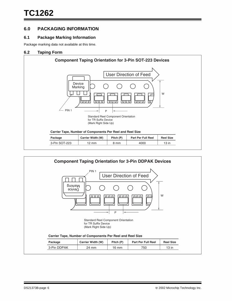
6.2 Taping Form
Component Taping Orientation for 3-Pin SOT-223 Devices
Package Carrier Width (W) Pitch (P) Part Per Full Reel Reel Size
3-Pin SOT-223 12 mm 8 mm 4000 13 in
Carrier Tape, Number of Components Per Reel and Reel Size
User Direction of Feed
DeviceMarking
PIN 1
Standard Reel Component Orientationfor TR Suffix Device(Mark Right Side Up)
W
P
Component Taping Orientation for 3-Pin DDPAK Devices
Package Carrier Width (W) Pitch (P) Part Per Full Reel Reel Size
3-Pin DDPAK 24 mm 16 mm 750 13 in
Carrier Tape, Number of Components Per Reel and Reel Size
User Direction of Feed
DeviceMarking
PIN 1
Standard Reel Component Orientationfor TR Suffix Device(Mark Right Side Up)
W
P
2002 Microchip Technology Inc. DS21373B-page 7
TC1262
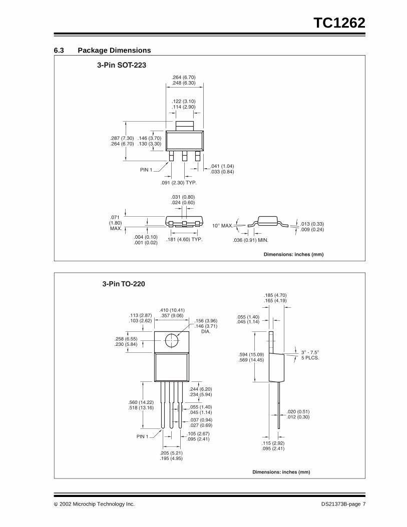
6.3 Package Dimensions
.264 (6.70)
.248 (6.30)
.122 (3.10)
.114 (2.90)
.287 (7.30)
.264 (6.70).146 (3.70).130 (3.30)
.091 (2.30) TYP.
.071 (1.80) MAX.
.181 (4.60) TYP. .036 (0.91) MIN.
.041 (1.04)
.033 (0.84)PIN 1
.013 (0.33)
.009 (0.24)
.031 (0.80)
.024 (0.60)
.004 (0.10)
.001 (0.02)
10° MAX.
3-Pin SOT-223
Dimensions: inches (mm)
3-Pin TO-220
.205 (5.21)
.195 (4.95)
PIN 1
.113 (2.87)
.103 (2.62)
.410 (10.41).357 (9.06)
.156 (3.96)
.146 (3.71)DIA.
.258 (6.55)
.230 (5.84)
.560 (14.22)
.518 (13.16)
.105 (2.67)
.095 (2.41)
.037 (0.94)
.027 (0.69)
.055 (1.40)
.045 (1.14)
.244 (6.20)
.234 (5.94)
.185 (4.70)
.165 (4.19)
.055 (1.40)
.045 (1.14)
.594 (15.09)
.569 (14.45)
.115 (2.92)
.095 (2.41)
.020 (0.51)
.012 (0.30)
3° - 7.5°5 PLCS.
Dimensions: inches (mm)

TC1262
DS21373B-page 8 2002 Microchip Technology Inc.
6.3 Package Dimensions (Continued)
.100 (2.54) TYP.
3-Pin DDPAK
.037 (0.94)
.026 (0.66)
.370 (9.40)
.330 (8.38)
.067 (1.70)
.045 (1.14)
.605 (15.37)
.549 (13.95)
.410 (10.41).385 (9.78)
.183 (4.65)
.170 (4.32)
.055 (1.40)
.045 (1.14)
.010 (0.25)
.000 (0.00)
.110 (2.79)
.068 (1.72)
.026 (0.66)
.014 (0.36).051 (1.30).049 (1.24)
8° MAX.
3° - 7°(5x)
PIN 1
Dimensions: inches (mm)
2002 Microchip Technology Inc. DS21373B-page 9
TC1262
SALES AND SUPPORT
Data SheetsProducts supported by a preliminary Data Sheet may have an errata sheet describing minor operational differences and recom-mended workarounds. To determine if an errata sheet exists for a particular device, please contact one of the following:
1. Your local Microchip sales office2. The Microchip Corporate Literature Center U.S. FAX: (480) 792-72773. The Microchip Worldwide Site (www.microchip.com)
Please specify which device, revision of silicon and Data Sheet (include Literature #) you are using.
New Customer Notification SystemRegister on our web site (www.microchip.com/cn) to receive the most current information on our products.
TC1262
DS21373B-page 10 2002 Microchip Technology Inc.
NOTES:
2002 Microchip Technology Inc. DS21373B-page 11
TC1262
Information contained in this publication regarding deviceapplications and the like is intended through suggestion onlyand may be superseded by updates. It is your responsibility toensure that your application meets with your specifications.No representation or warranty is given and no liability isassumed by Microchip Technology Incorporated with respectto the accuracy or use of such information, or infringement ofpatents or other intellectual property rights arising from suchuse or otherwise. Use of Microchip’s products as critical com-ponents in life support systems is not authorized except withexpress written approval by Microchip. No licenses are con-veyed, implicitly or otherwise, under any intellectual propertyrights.
Trademarks
The Microchip name and logo, the Microchip logo, FilterLab,KEELOQ, microID, MPLAB, PIC, PICmicro, PICMASTER,PICSTART, PRO MATE, SEEVAL and The Embedded ControlSolutions Company are registered trademarks of Microchip Tech-nology Incorporated in the U.S.A. and other countries.
dsPIC, ECONOMONITOR, FanSense, FlexROM, fuzzyLAB,In-Circuit Serial Programming, ICSP, ICEPIC, microPort,Migratable Memory, MPASM, MPLIB, MPLINK, MPSIM,MXDEV, MXLAB, PICC, PICDEM, PICDEM.net, rfPIC, SelectMode and Total Endurance are trademarks of MicrochipTechnology Incorporated in the U.S.A.
Serialized Quick Turn Programming (SQTP) is a service markof Microchip Technology Incorporated in the U.S.A.
All other trademarks mentioned herein are property of theirrespective companies.
© 2002, Microchip Technology Incorporated, Printed in theU.S.A., All Rights Reserved.
Printed on recycled paper.
Microchip received QS-9000 quality systemcertification for its worldwide headquarters,design and wafer fabrication facilities inChandler and Tempe, Arizona in July 1999and Mountain View, California in March 2002.The Company’s quality system processes andprocedures are QS-9000 compliant for itsPICmicro® 8-bit MCUs, KEELOQ® code hoppingdevices, Serial EEPROMs, microperipherals,non-volatile memory and analog products. Inaddition, Microchip’s quality system for thedesign and manufacture of developmentsystems is ISO 9001 certified.
DS21373B-page 12 2002 Microchip Technology Inc.
AMERICASCorporate Office2355 West Chandler Blvd.Chandler, AZ 85224-6199Tel: 480-792-7200 Fax: 480-792-7277Technical Support: 480-792-7627Web Address: http://www.microchip.comRocky Mountain2355 West Chandler Blvd.Chandler, AZ 85224-6199Tel: 480-792-7966 Fax: 480-792-7456
Atlanta500 Sugar Mill Road, Suite 200BAtlanta, GA 30350Tel: 770-640-0034 Fax: 770-640-0307Boston2 Lan Drive, Suite 120Westford, MA 01886Tel: 978-692-3848 Fax: 978-692-3821Chicago333 Pierce Road, Suite 180Itasca, IL 60143Tel: 630-285-0071 Fax: 630-285-0075Dallas4570 Westgrove Drive, Suite 160Addison, TX 75001Tel: 972-818-7423 Fax: 972-818-2924DetroitTri-Atria Office Building32255 Northwestern Highway, Suite 190Farmington Hills, MI 48334Tel: 248-538-2250 Fax: 248-538-2260Kokomo2767 S. Albright RoadKokomo, Indiana 46902Tel: 765-864-8360 Fax: 765-864-8387Los Angeles18201 Von Karman, Suite 1090Irvine, CA 92612Tel: 949-263-1888 Fax: 949-263-1338New York150 Motor Parkway, Suite 202Hauppauge, NY 11788Tel: 631-273-5305 Fax: 631-273-5335San JoseMicrochip Technology Inc.2107 North First Street, Suite 590San Jose, CA 95131Tel: 408-436-7950 Fax: 408-436-7955Toronto6285 Northam Drive, Suite 108Mississauga, Ontario L4V 1X5, CanadaTel: 905-673-0699 Fax: 905-673-6509
ASIA/PACIFICAustraliaMicrochip Technology Australia Pty LtdSuite 22, 41 Rawson StreetEpping 2121, NSWAustraliaTel: 61-2-9868-6733 Fax: 61-2-9868-6755China - BeijingMicrochip Technology Consulting (Shanghai)Co., Ltd., Beijing Liaison OfficeUnit 915Bei Hai Wan Tai Bldg.No. 6 Chaoyangmen BeidajieBeijing, 100027, No. ChinaTel: 86-10-85282100 Fax: 86-10-85282104China - ChengduMicrochip Technology Consulting (Shanghai)Co., Ltd., Chengdu Liaison OfficeRm. 2401, 24th Floor,Ming Xing Financial TowerNo. 88 TIDU StreetChengdu 610016, ChinaTel: 86-28-86766200 Fax: 86-28-86766599China - FuzhouMicrochip Technology Consulting (Shanghai)Co., Ltd., Fuzhou Liaison OfficeUnit 28F, World Trade PlazaNo. 71 Wusi RoadFuzhou 350001, ChinaTel: 86-591-7503506 Fax: 86-591-7503521China - ShanghaiMicrochip Technology Consulting (Shanghai)Co., Ltd.Room 701, Bldg. BFar East International PlazaNo. 317 Xian Xia RoadShanghai, 200051Tel: 86-21-6275-5700 Fax: 86-21-6275-5060China - ShenzhenMicrochip Technology Consulting (Shanghai)Co., Ltd., Shenzhen Liaison OfficeRm. 1315, 13/F, Shenzhen Kerry Centre,Renminnan LuShenzhen 518001, ChinaTel: 86-755-2350361 Fax: 86-755-2366086China - Hong Kong SARMicrochip Technology Hongkong Ltd.Unit 901-6, Tower 2, Metroplaza223 Hing Fong RoadKwai Fong, N.T., Hong KongTel: 852-2401-1200 Fax: 852-2401-3431IndiaMicrochip Technology Inc.India Liaison OfficeDivyasree Chambers1 Floor, Wing A (A3/A4)No. 11, O’Shaugnessey RoadBangalore, 560 025, IndiaTel: 91-80-2290061 Fax: 91-80-2290062
JapanMicrochip Technology Japan K.K.Benex S-1 6F3-18-20, ShinyokohamaKohoku-Ku, Yokohama-shiKanagawa, 222-0033, JapanTel: 81-45-471- 6166 Fax: 81-45-471-6122
KoreaMicrochip Technology Korea168-1, Youngbo Bldg. 3 FloorSamsung-Dong, Kangnam-KuSeoul, Korea 135-882Tel: 82-2-554-7200 Fax: 82-2-558-5934SingaporeMicrochip Technology Singapore Pte Ltd.200 Middle Road#07-02 Prime CentreSingapore, 188980Tel: 65-6334-8870 Fax: 65-6334-8850TaiwanMicrochip Technology Taiwan11F-3, No. 207Tung Hua North RoadTaipei, 105, TaiwanTel: 886-2-2717-7175 Fax: 886-2-2545-0139
EUROPEDenmarkMicrochip Technology Nordic ApSRegus Business CentreLautrup hoj 1-3Ballerup DK-2750 DenmarkTel: 45 4420 9895 Fax: 45 4420 9910FranceMicrochip Technology SARLParc d’Activite du Moulin de Massy43 Rue du Saule TrapuBatiment A - ler Etage91300 Massy, FranceTel: 33-1-69-53-63-20 Fax: 33-1-69-30-90-79GermanyMicrochip Technology GmbHGustav-Heinemann Ring 125D-81739 Munich, GermanyTel: 49-89-627-144 0 Fax: 49-89-627-144-44ItalyMicrochip Technology SRLCentro Direzionale ColleoniPalazzo Taurus 1 V. Le Colleoni 120041 Agrate BrianzaMilan, ItalyTel: 39-039-65791-1 Fax: 39-039-6899883United KingdomMicrochip Ltd.505 Eskdale RoadWinnersh TriangleWokinghamBerkshire, England RG41 5TUTel: 44 118 921 5869 Fax: 44-118 921-5820
05/01/02
*DS21373B*
WORLDWIDE SALES AND SERVICE