61800-3 (2004)
TRANSCRIPT
BRITISH STANDARD
BS EN 61800-3:2004Adjustable speed electrical power drive systems —
Part 3: EMC requirements and specific test methods
The European Standard EN 61800-3:2004 has the status of a British Standard
ICS 29.200; 33.100
BS EN 61800-3:2004
This British Standard was published under the authority of the Standards Policy and Strategy Committee on 4 February 2005
© BSI 4 February 2005
ISBN 0 580 45367 7
National forewordThis British Standard is the official English language version of EN 61800-3:2004. It is identical with IEC 61800-3:2004. It supersedes BS EN 61800-3:1997 which will be withdrawn on 2007-10-01.
The UK participation in its preparation was entrusted to Technical Committee PEL/22, Power supply systems, which has the responsibility to:
A list of organizations represented on this committee can be obtained on request to its secretary.
Cross-referencesThe British Standards which implement international or European publications referred to in this document may be found in the BSI Catalogue under the section entitled “International Standards Correspondence Index”, or by using the “Search” facility of the BSI Electronic Catalogue or of British Standards Online.
This publication does not purport to include all the necessary provisions of a contract. Users are responsible for its correct application.
Compliance with a British Standard does not of itself confer immunity from legal obligations.
— aid enquirers to understand the text;
— present to the responsible international/European committee any enquiries on the interpretation, or proposals for change, and keep the UK interests informed;
— monitor related international and European developments and promulgate them in the UK.
Summary of pages
This document comprises a front cover, an inside front cover, the EN title page, pages 2 to 119 and a back cover.
The BSI copyright notice displayed in this document indicates when the document was last issued.
Amendments issued since publication
Amd. No. Date Comments
EUROPEAN STANDARD EN 61800-3
NORME EUROPÉENNE
EUROPÄISCHE NORM December 2004
CENELEC European Committee for Electrotechnical Standardization
Comité Européen de Normalisation Electrotechnique Europäisches Komitee für Elektrotechnische Normung
Central Secretariat: rue de Stassart 35, B - 1050 Brussels
© 2004 CENELEC - All rights of exploitation in any form and by any means reserved worldwide for CENELEC members.
Ref. No. EN 61800-3:2004 E
ICS 29.200 ; 33.100 Supersedes EN 61800-3:1996 + A11:2000
English version
Adjustable speed electrical power drive systems Part 3: EMC requirements and specific test methods
(IEC 61800-3:2004) Entraînements électriques de puissance à vitesse variable Partie 3: Exigences de CEM et méthodes d'essais spécifiques (CEI 61800-3:2004)
Drehzahlveränderbare elektrische Antriebe Teil 3: EMV-Anforderungen einschließlich spezieller Prüfverfahren (IEC 61800-3:2004)
This European Standard was approved by CENELEC on 2004-10-01. CENELEC members are bound to comply with the CEN/CENELEC Internal Regulations which stipulate the conditions for giving this European Standard the status of a national standard without any alteration. Up-to-date lists and bibliographical references concerning such national standards may be obtained on application to the Central Secretariat or to any CENELEC member. This European Standard exists in three official versions (English, French, German). A version in any other language made by translation under the responsibility of a CENELEC member into its own language and notified to the Central Secretariat has the same status as the official versions. CENELEC members are the national electrotechnical committees of Austria, Belgium, Cyprus, Czech Republic, Denmark, Estonia, Finland, France, Germany, Greece, Hungary, Iceland, Ireland, Italy, Latvia, Lithuania, Luxembourg, Malta, Netherlands, Norway, Poland, Portugal, Slovakia, Slovenia, Spain, Sweden, Switzerland and United Kingdom.
Foreword
The text of document 22G/127/FDIS, future edition 2 of IEC 61800-3, prepared by SC 22G, Adjustable speed electric drive systems incorporating semiconductor power converters, of IEC TC 22, Power electronic systems and equipment, was submitted to the IEC-CENELEC parallel vote and was approved by CENELEC as EN 61800-3 on 2004-10-01.
This European Standard supersedes EN 61800-3:1996 + A11:2000 + corrigendum May 2001.
This European Standard introduces three main changes:
a) the classes of distribution (unrestricted and restricted) of the PDS have been replaced by categories of PDS (C1 to C4) with definitions related to the product itself and its intended use;
b) better coverage of emission limits;
c) an EMC plan is generalized for category C4.
The following dates were fixed:
– latest date by which the EN has to be implemented at national level by publication of an identical national standard or by endorsement
(dop)
2005-07-01
– latest date by which the national standards conflicting with the EN have to be withdrawn
(dow)
2007-10-01
This European Standard has been prepared under a mandate given to CENELEC by the European Commission and the European Free Trade Association and covers essential requirements of Directive 89/336/EEC. See Annex ZZ.
Annexes ZA and ZZ have been added by CENELEC.
__________
Page 2EN 61800−3:2004
Endorsement notice
The text of the International Standard IEC 61800-3:2004 was approved by CENELEC as a European Standard without any modification.
In the official version, for Bibliography, the following notes have to be added for the standards indicated:
IEC 60038 NOTE Harmonized as HD 472 S1:1989 (modified).
IEC 60146-1-3 NOTE Harmonized as EN 60146-1-3:1993 (not modified).
IEC 60146-2 NOTE Harmonized as EN 60146-2:2000 (not modified).
IEC 61000-2-12 NOTE Harmonized as EN 61000-2-12:2003 (not modified).
IEC 61000-4-1 NOTE Harmonized as EN 61000-4-1:2000 (not modified).
IEC 61000-4-7 NOTE Harmonized as EN 61000-4-7:2000 (not modified).
IEC 61000-4-9 NOTE Harmonized as EN 61000-4-9:1993 (not modified).
IEC 61000-4-10 NOTE Harmonized as EN 61000-4-10:1993 (not modified).
IEC 61000-6-1 NOTE Harmonized as EN 61000-6-1:2001 (modified).
IEC 61000-6-2 NOTE Harmonized as EN 61000-6-2:1999 (not modified).
IEC 61000-6-4 NOTE Harmonized as EN 61000-6-4:2001 (modified).
IEC 61800-5-1 NOTE Harmonized as EN 61800-5-1:2003 (not modified).
__________
Page 3EN 61800−3:2004
CONTENTS
1 Scope and object..............................................................................................................8 2 Normative references .......................................................................................................9 3 Terms and definitions ..................................................................................................... 11 4 Common requirements ................................................................................................... 16
4.1 General conditions ................................................................................................ 16 4.2 Tests ..................................................................................................................... 17 4.3 Documentation for the user ................................................................................... 17
5 Immunity requirements ................................................................................................... 18 5.1 General conditions ................................................................................................ 18 5.2 Basic immunity requirements – Low-frequency disturbances ................................. 21 5.3 Basic immunity requirements – High-frequency disturbances................................. 26 5.4 Application of immunity requirements – statistical aspect ...................................... 29
6 Emission ........................................................................................................................ 30 6.1 General emission requirements ............................................................................. 30 6.2 Basic low-frequency emission limits ...................................................................... 30 6.3 Conditions related to high-frequency emission measurement ................................ 33 6.4 Basic high-frequency emission limits ..................................................................... 34 6.5 Engineering practice.............................................................................................. 37 6.6 Application of emission requirements – statistical aspects ..................................... 41
Annex A (informative) EMC techniques ................................................................................ 42 A.1 General overview of EMC phenomena ............................................................................ 42 A.2 Load conditions regarding high-frequency phenomena ................................................... 45 A.3 Some immunity aspects .................................................................................................. 46 A.4 High-frequency emission measurement techniques ........................................................ 47 Annex B (informative) Low-frequency phenomena ............................................................... 52 B.1 Commutation notches ..................................................................................................... 52 B.2 Definitions related to harmonics and interharmonics ....................................................... 57 B.3 Application of harmonic emission standards ................................................................... 63 B.4 Installation rules/Assessment of harmonic compatibility.................................................. 72 B.5 Voltage unbalance..........................................................................................................77 B.6 Voltage dips – Voltage fluctuations ................................................................................. 80 B.7 Verification of immunity to low frequency disturbances ................................................... 82 Annex C (informative) Reactive power compensation – filtering ........................................... 84 C.1 Installation...................................................................................................................... 84 C.2 Reactive power and harmonics ....................................................................................... 92
Page 4EN 61800−3:2004
Annex D (informative) Considerations on high-frequency emission ...................................... 96 D.1 User guidelines .............................................................................................................. 96 D.2 Safety and RFI-filtering in power supply systems.......................................................... 100 Annex E (informative) EMC analysis and EMC plan ........................................................... 102 E.1 General – System EMC analysis applied to PDSs......................................................... 102 E.2 Example of EMC plan for general applications .............................................................. 105 E.3 Example of supplement to EMC plan for particular application ...................................... 109 Annex ZA (normative) Normative references to international publications with their
corresponding European publications ........................................................................... 113 Annex ZZ (informative) Coverage of Essential Requirements of EC Directives................... 116 Bibliography........................................................................................................................ 117 Figure 1 – Definition of the installation and its content .......................................................... 12 Figure 2 – Internal interfaces of the PDS and examples of ports ........................................... 14 Figure 3 – Power interfaces of a PDS with common d.c. BUS ............................................... 15 Figure 4 – Power interfaces with common input transformer ................................................. 15 Figure 5 – Propagation of disturbances................................................................................. 38 Figure 6 – Propagation of disturbances in installation with a PDS rated > 1 000 V ................ 39 Figure A.1 – Coordination between disturbance and immunity .............................................. 44 Figure B.1 – Typical waveform of commutation notches – Distinction from non-repetitive transient. ............................................................................................................... 52 Figure B.2 – PCC, IPC, Installation current ratio and RSI...................................................... 62 Figure B.3 – PCC, IPC, Installation current ratio and RSC .................................................... 63 Figure B.4 – Assessment of the harmonic emission of a PDS ............................................... 66 Figure B.5 – Load conditions for the measurement of harmonic emission of a PDS............... 67 Figure B.6 – Test set up with mechanical load ...................................................................... 68 Figure B.7 – Test set up with electrical load replacing the loaded motor ............................... 68 Figure B.8 – Test set up with resistive load........................................................................... 69 Figure B.9 – Assessment of harmonic emission where PDS are used (apparatus, systems or installations) ....................................................................................................... 73 Figure C.1 – Reactive power compensation .......................................................................... 87 Figure C.2 – Simplified diagram of an industrial network ....................................................... 89 Figure C.3 – Impedance versus frequency of the simplified network...................................... 89 Figure C.4 – Example of passive filter battery ....................................................................... 92 Figure C.5 – Example of inadequate solution in reactive power compensation ...................... 93 Figure D.1 – Conducted emission of various unfiltered PDSs ................................................ 97 Figure D.2 – Expected radiated emission of PDS up to rated voltage 400 V Peak values normalised at 10 m .................................................................................................... 98 Figure D.3 – Safety and filtering ......................................................................................... 101 Figure E.1 – Interaction between systems and EM environment .......................................... 102 Figure E.2 – Zone concept .................................................................................................. 103 Figure E.3 – Example of drive ............................................................................................. 207
Page 5EN 61800−3:2004
Table 1 – Criteria to prove the acceptance of a PDS against electromagnetic disturbances ......................................................................................................................... 19 Table 2 – Minimum immunity requirements for harmonics and commutation notches/voltage distortion on power ports of low voltage PDSs ............................................. 22 Table 3 – Minimum immunity requirements for harmonics and commutation notches/voltage distortion on main power ports of PDSs of rated voltage above 1 000 V ...... 22 Table 4 – Minimum immunity requirements for harmonics and commutation notches/voltage distortion on auxiliary low voltage power ports of PDSs ............................... 23 Table 5 – Minimum immunity requirements for voltage deviations, dips and short interruptions on power ports of low voltage PDSs ................................................................. 23 Table 6 – Minimum immunity requirements for voltage deviations, dips and short interruptions on main power ports of rated voltage above 1 000 V of PDSs ........................... 24 Table 7 – Minimum immunity requirements for voltage deviations, dips and short interruptions on auxiliary low voltage power ports of PDSs ................................................... 25 Table 8 – Minimum immunity requirements for voltage unbalance and frequency variations on power ports of low voltage PDSs...................................................................... 25 Table 9 – Minimum immunity requirements for voltage unbalance and frequency variations on main power ports of rated voltage above 1 000 V of PDSs ............................... 26 Table 10 – Minimum immunity requirements for voltage unbalance and frequency variations on auxiliary low voltage power ports of PDSs........................................................ 26 Table 11–Minimum immunity requirements for PDSs intended for use in the first environment .......................................................................................................................... 27 Table 12 – Minimum immunity requirements for PDSs intended for use in the second environment .......................................................................................................................... 28 Table 13 – Summary of emission requirements ..................................................................... 30 Table 14 – Limits for mains terminal disturbance voltage in the frequency band 150 kHz to 30 MHz ...................................................................................................................... 34 Table 15 – Limits for electromagnetic radiation disturbance in the frequency band 30 MHz to 1 000 MHz ................................................................................................................ 35 Table 16 – Limits of disturbance voltage on the power interface – Option 2 .......................... 36 Table 17 – Limits for mains terminal disturbance voltage in the frequency band 150 kHz to 30 MHz PDS in the second environment – PDS of category C3 ........................... 36 Table 18 – Limits for electromagnetic radiation disturbance in the frequency band 30 MHz to 1 000 MHz PDS in the second environment – PDS of category C3 ....................... 37 Table 19 – Limits for propagated disturbance voltage ("outside" in the first environment)......................................................................................................................... 40 Table 20 –Limits for propagated disturbance voltage ("outside" in the second environment)......................................................................................................................... 40 Table 21 – Limits for propagated electromagnetic disturbance above 30 MHz....................... 40 Table 22 – Limits for electromagnetic disturbance below 30 MHz.......................................... 41
Page 6EN 61800−3:2004

Table A.1 – EMC overview.................................................................................................... 43 Table B.1 – Maximum allowable depth of commutation notches at the PC............................. 56 Table B.2 – Harmonic current emission requirements relative to the total current of the agreed power at the PCC or IPC ........................................................................................... 75 Table B.3 – Verification plan for immunity to low frequency disturbances .............................. 83 Table E.1 – EM interaction between subsystems and environment...................................... 104 Table E.2 – Frequency analysis .......................................................................................... 111
Page 7EN 61800−3:2004
1 Scope and object
This part of IEC 61800 specifies electromagnetic compatibility (EMC) requirements for power drive systems (PDSs). A PDS is defined in 3.1. These are adjustable speed a.c. or d.c. motor drives. Requirements are stated for PDSs with converter input and/or output voltages (line-to-line voltage), up to 35 kV a.c. r.m.s.
PDSs covered by this standard are those installed in residential, commercial and industrial locations with the exception of traction applications, and electric vehicles. PDSs may be connected to either industrial or public power distribution networks. Industrial networks are supplied by a dedicated distribution transformer, which is usually adjacent to or inside the industrial location, and supplies only industrial customers. Industrial networks can also be supplied by their own electric generating equipment. On the other hand, PDSs can be directly connected to low-voltage public mains networks which also supply domestic premises, and in which the neutral is generally earthed (grounded).
The scope of this part of IEC 61800, related to EMC, includes a broad range of PDSs from a few hundred watts to hundreds of megawatts. PDSs are often included in a larger system. The system aspect is not covered by this standard but guidance is provided in the informative annexes.
The requirements have been selected so as to ensure EMC for PDSs at residential, commercial and industrial locations. The requirements cannot, however, cover extreme cases which may occur with an extremely low probability. Changes in the EMC behaviour of a PDS, as a result of fault conditions, are not taken into account.
The object of this standard is to define the limits and test methods for a PDS according to its intended use. This standard includes immunity requirements and requirements for electro-magnetic emissions.
NOTE 1 Emission can cause interference in other electronic equipment (for example radio receivers, measuring and computing devices). Immunity is required to protect the equipment from continuous and transient conducted and radiated disturbances including electrostatic discharges. The emission and immunity requirements are balanced against each other and against the actual environment of the PDS.
This standard defines the minimum EMC requirements for a PDS.
Immunity requirements are given according to the environment classification. Low-frequency emission requirements are given according to the nature of the supply network. High-frequency emission requirements are given according to four categories of intended use, which cover both environment and bringing into operation.
As a product standard, this standard may be used for the assessment of PDS. It may also be used for the assessment of CDM or BDM (see 3.1), which can be marketed separately.
Page 8EN 61800−3:2004
This standard contains:
– conformity assessment requirements for products to be placed on the market; – recommended engineering practice (see 6.5) for cases where high frequency emissions
cannot be measured before the equipment is placed on the market (such PDSs are defined in 3.2.6 as category C4).
NOTE 2 The first edition of IEC 61800-3 identified that the intended use could require engineering for putting into service. This was done by the “restricted distribution mode”. Equipment that used to be covered by the “restricted distribution mode” is covered in the second edition by categories C2 and C4 (see 3.2).
This standard is intended as a complete EMC product standard for the EMC conformity assessment of products of categories C1, C2 and C3, when placing them on the market (see definitions 3.2.3 to 3.2.5).
Radio frequency emission of equipment of category C4 is only assessed when it is installed in its intended location. It is therefore treated as a fixed installation, for which this standard gives rules of engineering practice in 6.5 and annex E, although it gives no defined emission limits (except in case of complaint).
This standard does not specify any safety requirements for the equipment such as protection against electric shocks, insulation co-ordination and related dielectric tests, unsafe operation, or unsafe consequences of a failure. It also does not cover safety and functional safety implications of electromagnetic phenomena.
In special cases, when highly susceptible apparatus is being used in proximity, additional mitigation measures may have to be employed to reduce the electromagnetic emission further below the specified levels or additional countermeasures may have to be employed to increase the immunity of the highly susceptible apparatus.
As an EMC product standard for PDSs, this standard takes precedence over all aspects of the generic standards and no additional EMC tests are required or necessary. If a PDS is included as part of equipment covered by a separate EMC product standard, the EMC standard of the complete equipment applies.
2 Normative references
The following referenced documents are indispensable for the application of this document. For dated references, only the edition cited applies. For undated references, the latest edition of the referenced document (including any amendments) applies.
IEC 60050 (131):2002, International Electrotechnical Vocabulary (IEV) – Chapter 131: Circuit theory
IEC 60050 (151):2001, International Electrotechnical Vocabulary (IEV) – Chapter 151: Electrical and magnetic devices
IEC 60050 (161):1990, International Electrotechnical Vocabulary (IEV) – Chapter 161: Electromagnetic compatibility
IEC 60146-1-1:1991, Semiconductor convertors – General requirements and line commutated convertors – Part 1-1: Specifications of basic requirements
Page 9EN 61800−3:2004
IEC 60364-1:2001, Electrical installations of buildings – Part 1: Fundamental principles, assessment of general characteristics, definitions
IEC 60664-1:1992, Insulation co-ordination for equipment within low-voltage systems – Part 1: Principles, requirements and tests
IEC 61000-1-1, Electromagnetic compatibility (EMC) – Part 1: General – Section 1: Application and interpretation of fundamental definitions and terms
IEC 61000-2-1:1990, Electromagnetic compatibility (EMC) – Part 2: Environment – Section 1: Description of the environment – Electromagnetic environment for low-frequency conducted disturbances and signalling in public power supply systems
IEC 61000-2-2:2002, Electromagnetic compatibility (EMC) – Part 2: Environment – Section 2: Compatibility levels for low-frequency conducted disturbances and signalling in public low-voltage power supply systems
IEC 61000-2-4:2003, Electromagnetic compatibility (EMC) – Part 2: Environment – Section 4: Compatibility levels in industrial plants for low-frequency conducted disturbances
IEC 61000-2-6:1995, Electromagnetic compatibility (EMC) – Part 2: Environment – Section 6: Assessment of the emission levels in the power supply of industrial plants as regards low-frequency conducted disturbances
IEC 61000-3-2:2000, Electromagnetic compatibility (EMC) – Part 3: Limits – Section 2: Limits for harmonic current emissions (equipment with input current < 16 A per phase)
IEC 61000-3-3:1994, Electromagnetic compatibility (EMC) – Part 3-3: Limits – Limitation of voltage changes, voltage fluctuations and flicker in public low-voltage supply systems for equipment with rated current ≤ 16 A per phase and subject to conditional connection
IEC 61000-3-4:1998, Electromagnetic compatibility (EMC) – Part 3: Limits – Section 4: Limitation of emission of harmonic currents in low-voltage power supply systems for equipment with rated current greater than 16 A
IEC 61000-3-7:1996, Electromagnetic compatibility (EMC) – Part 3: Limits – Section 7: Limits for fluctuating loads in MV and HV power systems – Basic EMC publication
IEC 61000-3-11:2000, Electromagnetic compatibility (EMC) – Part 3-11: Limits – Limitation of voltage changes, voltage fluctuations and flicker in public low-voltage supply systems for equipment with rated current ≤ 75 A and subject to conditional connection
IEC 61000-4-2, Electromagnetic compatibility (EMC) – Part 4-2: Testing and measurement techniques – Electrostatic discharge immunity test Basic EMC publication
IEC 61000-4-3:2002, Electromagnetic compatibility (EMC) – Part 4-3: Testing and measure-ment techniques – Radiated, radio-frequency, electromagnetic field immunity test Basic EMC publication
IEC 61000-4-4:1995, Electromagnetic compatibility (EMC) – Part 4: Testing and measurement techniques – Section 4: Electrical fast transient/burst immunity test Basic EMC publication Amendment 1 (2000) Amendment 2 (2001)
IEC 61000-4-5:1995, Electromagnetic compatibility (EMC) – Part 4: Testing and measurement techniques – Section 5: Surge immunity test
Page 10EN 61800−3:2004
IEC 61000-4-6:2003, Electromagnetic compatibility (EMC) – Part 4-6: Testing and measure-ment techniques – Immunity to conducted disturbances, induced by radio-frequency fields
IEC 61000-4-8:2001, Electromagnetic compatibility (EMC) – Part 4-8: Testing and measure-ment techniques – Power frequency magnetic field immunity test Basic EMC publication
IEC 61800-1:1997, Adjustable speed electrical power drive systems – Part 1: Rating specifications for low voltage d.c. power drive systems
IEC 61800-2:1998, Adjustable speed electrical power drive systems – Part 2: General requirements – Rating specifications for low voltage adjustable frequency a.c. power drive systems
IEC 61800-4:2002, Adjustable speed electrical power drive systems – Part 4: General requirements – Rating specifications for a.c. power drive systems above 1000 V and not exceeding 35 kV
CISPR 11:2003, Industrial, scientific and medical (ISM) radio-frequency equipment – Electromagnetic disturbance characteristics – Limits and methods of measurement
CISPR 14, Electromagnetic compatibility – Requirements for household appliances, electric tools and similar apparatus
CISPR 16-1:2002, Specification for radio disturbance and immunity measuring apparatus and methods – Part 1: Radio disturbance and immunity measuring apparatus
CISPR 22:2003, Information technology equipment – Radio disturbance characteristics – Limits and methods of measurement
3 Terms and definitions
3.1 Overview
For the purposes of this document, definitions related to EMC and to relevant phenomena to be found in IEC 60050(161), in CISPR, and also, the following additional definitions apply.
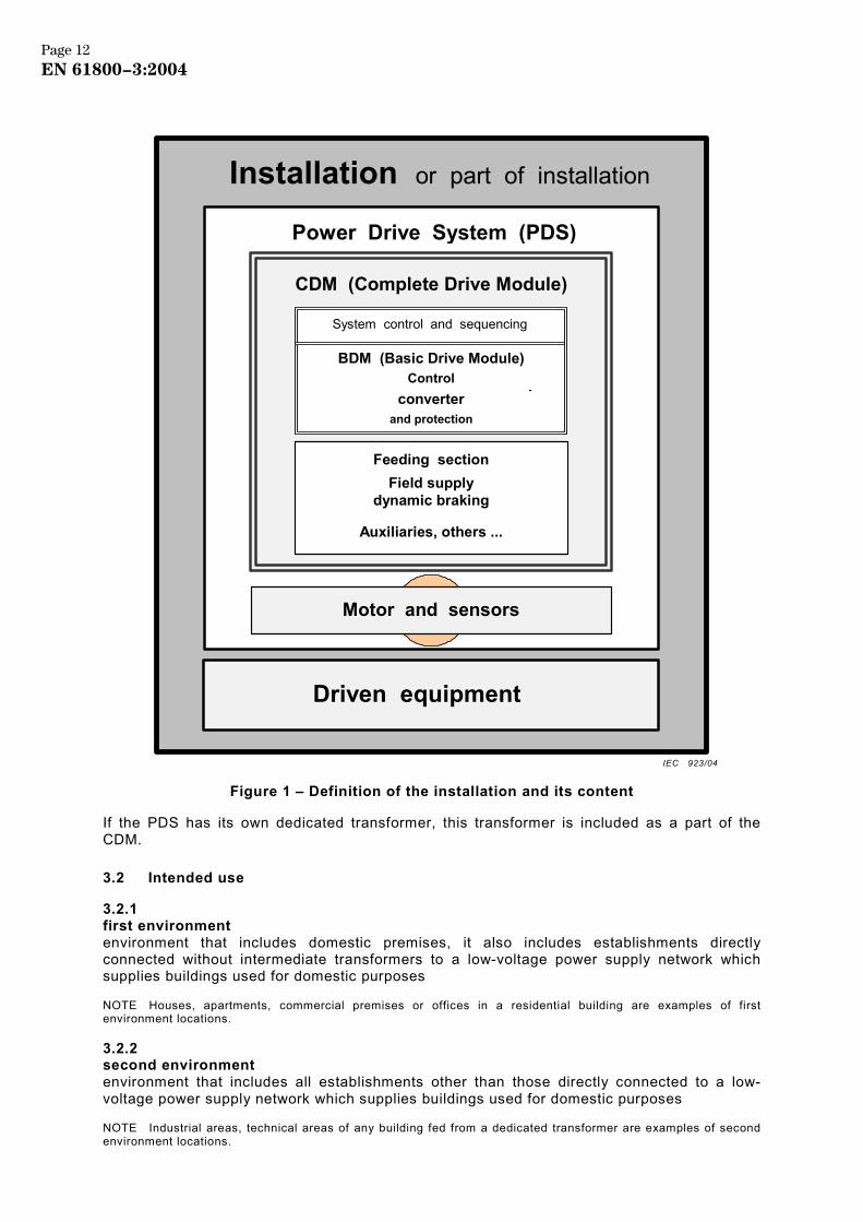
A power drive system (PDS) consists of a motor and a complete drive module (CDM). It does not include the equipment driven by the motor. The CDM consists of a basic drive module (BDM) and its possible extensions such as the feeding section or some auxiliaries (e.g. ventilation). The BDM contains converter, control and self-protection functions. Figure 1 shows the boundary between the PDS and the rest of the installation and/or manufacturing process. IEC 61800-1, IEC 61800-2 and IEC 61800-4 give details for these definitions.
Page 11EN 61800−3:2004
Installation or part of installation Power Drive System (PDS)
CDM (Complete Drive Module)
Driven equipment
Feeding section Field supply
dynamic braking
Auxiliaries, others ...
Motor and sensors
BDM (Basic Drive Module) Control
converterand protection
System control and sequencing
Figure 1 – Definition of the installation and its content
If the PDS has its own dedicated transformer, this transformer is included as a part of the CDM.
3.2 Intended use
3.2.1 first environment environment that includes domestic premises, it also includes establishments directly connected without intermediate transformers to a low-voltage power supply network which supplies buildings used for domestic purposes
NOTE Houses, apartments, commercial premises or offices in a residential building are examples of first environment locations.
3.2.2 second environment environment that includes all establishments other than those directly connected to a low-voltage power supply network which supplies buildings used for domestic purposes
NOTE Industrial areas, technical areas of any building fed from a dedicated transformer are examples of second environment locations.
IEC 923/04
Page 12EN 61800−3:2004
3.2.3 PDS of category C1 PDS of rated voltage less than 1 000 V, intended for use in the first environment
3.2.4 PDS of category C2 PDS of rated voltage less than 1 000 V, which is neither a plug in device nor a movable device and, when used in the first environment, is intended to be installed and commissioned only by a professional
NOTE A professional is a person or an organisation having necessary skills in installing and/or commissioning power drive systems, including their EMC aspects.
3.2.5 PDS of category C3 PDS of rated voltage less than 1 000 V, intended for use in the second environment and not intended for use in the first environment
3.2.6 PDS of category C4 PDS of rated voltage equal to or above 1 000 V, or rated current equal to or above 400 A, or intended for use in complex systems in the second environment
3.3 Location, ports and interfaces
3.3.1 in situ (for test) location where the equipment is installed for its normal use by the end user
3.3.2 test site (radiation) a site meeting requirements necessary for correctly measuring, under defined conditions, electromagnetic fields emitted by a device under test
[IEV 161-04-28]
3.3.3 port access to a device or network where electromagnetic energy or signals may be supplied or received or where the device or network variables may be observed or measured
[IEV 131-12-60]
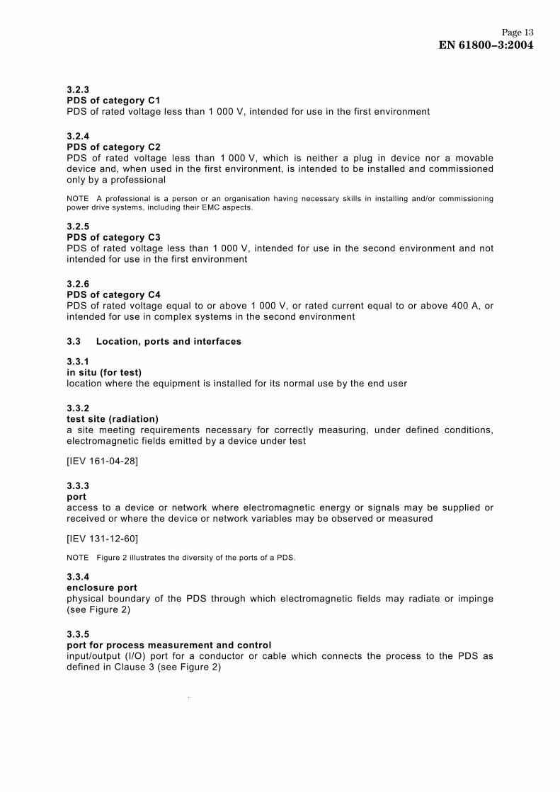
NOTE Figure 2 illustrates the diversity of the ports of a PDS.
3.3.4 enclosure port physical boundary of the PDS through which electromagnetic fields may radiate or impinge (see Figure 2)
3.3.5 port for process measurement and control input/output (I/O) port for a conductor or cable which connects the process to the PDS as defined in Clause 3 (see Figure 2)
Page 13EN 61800−3:2004
3.3.6 power port port which connects the PDS to the power supply which also feeds other equipment
3.3.7 main power port power port which feeds the PDS for only the power which, after electrical power conversion, is converted by the motor into mechanical power
3.3.8 auxiliary power port power port which feeds only the auxiliaries of the PDS, including the field circuit if any
3.3.9 mechanical link mechanical connection between the shaft of the motor of the PDS and the driven equipment of the process as defined in Clause 3
3.3.10 signal interface input/output (I/O) connection for a line connecting the basic drive module or complete drive module (BDM/CDM) to another part of the PDS (see Figure 2)
BDMor part of
CDM
PDS
Other part ofPDS
e.g. motor
Other part of
CDM or PDSSignal interface
Power interface
Enclosure port
Main power port
Processmeasurement and
control port
Earth port
Auxiliary power port
Figure 2 – Internal interfaces of the PDS and examples of ports
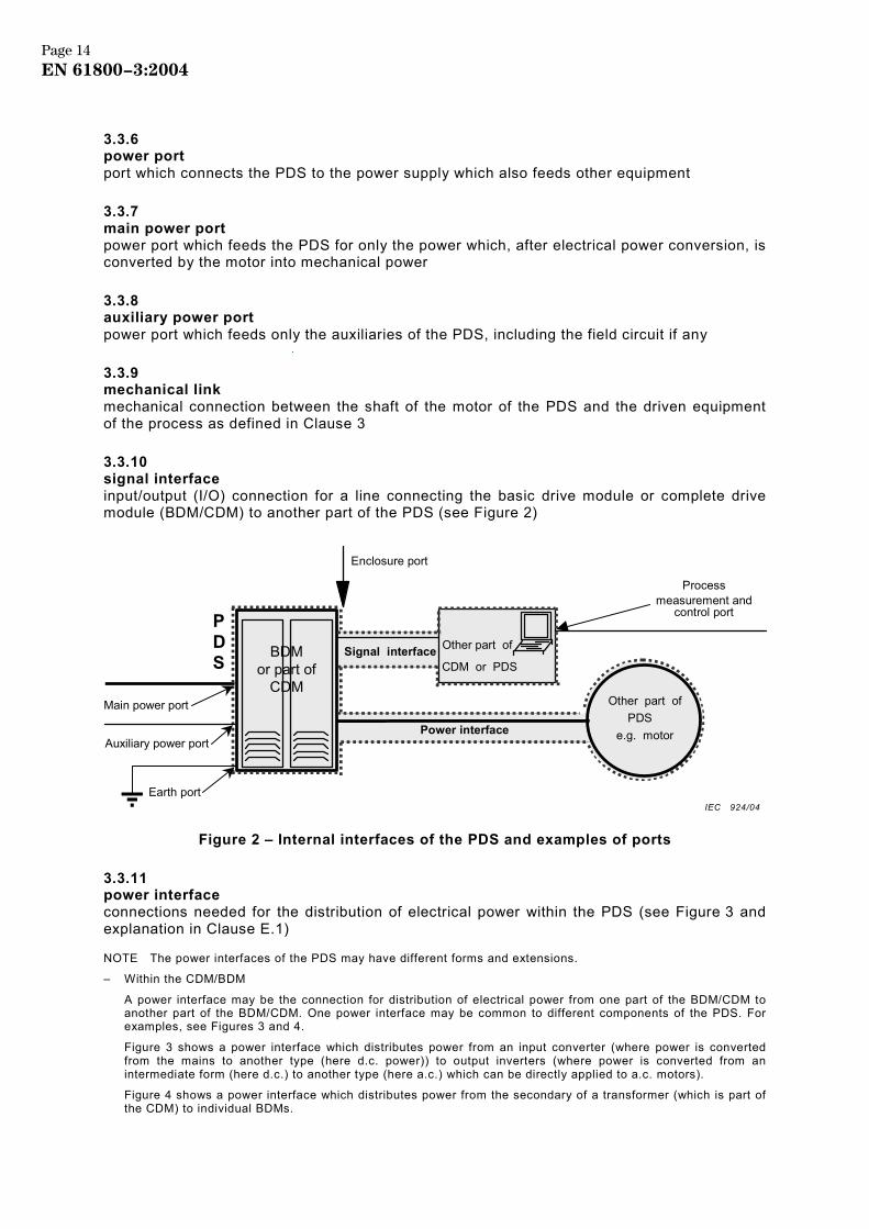
3.3.11 power interface connections needed for the distribution of electrical power within the PDS (see Figure 3 and explanation in Clause E.1)
NOTE The power interfaces of the PDS may have different forms and extensions.
– Within the CDM/BDM
A power interface may be the connection for distribution of electrical power from one part of the BDM/CDM to another part of the BDM/CDM. One power interface may be common to different components of the PDS. For examples, see Figures 3 and 4.
Figure 3 shows a power interface which distributes power from an input converter (where power is converted from the mains to another type (here d.c. power)) to output inverters (where power is converted from an intermediate form (here d.c.) to another type (here a.c.) which can be directly applied to a.c. motors).
Figure 4 shows a power interface which distributes power from the secondary of a transformer (which is part of the CDM) to individual BDMs.
IEC 924/04
Page 14EN 61800−3:2004
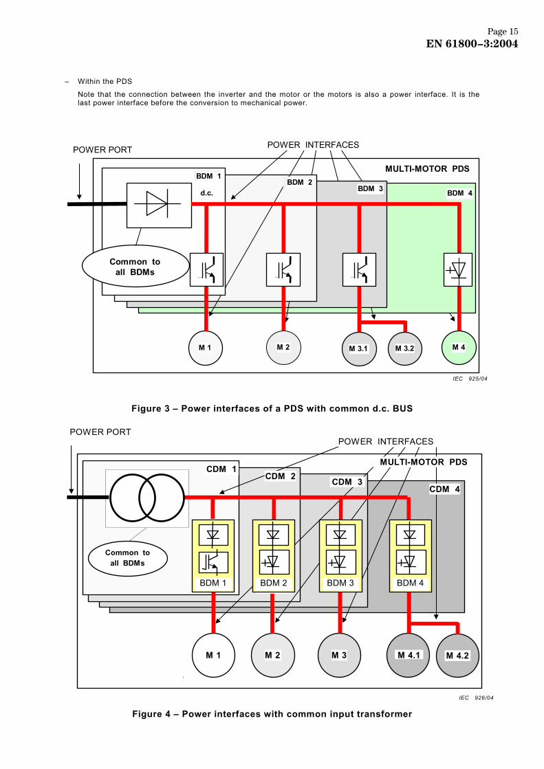
– Within the PDS
Note that the connection between the inverter and the motor or the motors is also a power interface. It is the last power interface before the conversion to mechanical power.
BDM 1BDM 3 BDM 4
M 2M 1
Common toall BDMs
d.c.
MULTI-MOTOR PDS
POWER PORT POWER INTERFACES
BDM 2
M 4M 3.2M 3.1
Figure 3 – Power interfaces of a PDS with common d.c. BUS
CDM 1
M 3M 1 M 4.1 M 4.2
Common toall BDMs
POWER PORTPOWER INTERFACES
MULTI-MOTOR PDSCDM 2 CDM 3
CDM 4
M 2
BDM 1BDM 1 BDM 1BDM 2 BDM 3 BDM 4
Figure 4 – Power interfaces with common input transformer
IEC 925/04
IEC 926/04
Page 15EN 61800−3:2004
3.3.12 PCC, IPC, PC these definitions are given in IEC 61000-2-4
NOTE Briefly:
– PCC is the point of common coupling on a public network;
– IPC is the in-plant point of coupling;
– PC is the point of coupling (for either of these cases).
3.4 Components of the PDS
3.4.1 converter (of the BDM) the unit which changes the form of electrical power supplied by the mains to the form fed to the motor(s) by changing one or more of the voltage, current and/or frequency
NOTE 1 The converter comprises electronic commutating devices and their associated commutation circuits. It is controlled by transistors or thyristors or any other power switching semiconductor devices.
NOTE 2 The converter can be line-commutated, load-commutated or self-commutated and can consist, for example, of one or more rectifiers or inverters.
3.4.2 (electric) motor electric machine intended to transform electric energy into mechanical energy
[IEV 151-13-41]
3.4.3 motor (of the PDS) for the purposes of this standard, the motor includes all sensors which are mounted on it and which are relevant for supporting the operating mode and interacting with a CDM
3.4.4 sub-component (of the PDS) for the purposes of this standard, a component of the PDS may be divided in sub-components, each of them being a physical piece of equipment which can be operated separately with an intrinsic function defined by the manufacturer
NOTE As an example, the control unit of a CDM may be a sub-component.
4 Common requirements
4.1 General conditions
All phenomena, from the emission or immunity point of view, shall be considered individually. The limits are given for conditions which do not consider the cumulative effects of different phenomena.
For a realistic assessment of the EMC situation, a typical configuration shall be chosen.
The application of tests for evaluation of immunity depends on the particular PDS, its configuration, its ports, its technology and its operating conditions (see annexes).
Page 16EN 61800−3:2004
4.2 Tests
4.2.1 Conditions
IEC 60146-1-1 and IEC 61800-2 distinguish between type test, routine test and special test. Unless otherwise stated, all the tests specified in this standard are type tests only. The equipment shall meet the EMC requirements when measured by the test methods specified in this standard.
NOTE Due to local radio transmission legislation, some immunity tests can be subject to conditions which restrict the choice of location where they can be performed.
If necessary, safeguards shall be taken against any unintended effects on the total process that may result from an equipment failure while an EMC test is being conducted.
For the tests, unless otherwise specified by the manufacturer, the CDM shall be connected to a standard motor of adequate ratings with a cable and earthing rules defined by the manufacturer. In some cases, passive load conditions (resistive, or resistive and inductive) may additionally be applied (for example, for evaluation of the low-frequency emissions).
The description of the tests, the test methods, the characteristics of the tests and the test set-ups are given in the referred standards and are not repeated here. If, however, modifications or additional requirements and information or specific test methods are needed for practical implementation and application of the tests, then they are given in this standard.
4.2.2 Test report
The test results shall be documented in a test report. The report shall clearly and unambiguously present all relevant information of the tests (for example: load conditions, cable laying, etc.). A functional description and detailed acceptance criteria provided by the manufacturer shall be noted in the test report.
Within the test report, the chosen test arrangements shall be justified. A sufficient number of terminals shall be selected to simulate actual operating conditions and to ensure that all relevant types of termination are covered. The tests shall be carried out at the rated supply voltage and in a reproducible manner.
4.3 Documentation for the user
The setting of limits and the structure of this standard are based on the understanding that the installer and user are responsible for following the EMC recommendations of the manufacturer.
The manufacturer shall supply the documentation necessary for the installer of a BDM, CDM, or for the user of a PDS for the correct installation into a typical system or process in the intended environment.
If special EMC measures are necessary to fulfil the required limits, these shall be clearly stated in the user documentation. Where relevant, these can include:
– maximum and minimum acceptable supply network impedance; – the use of shielded or special cables (power and/or control); – cable shield connection requirements; – maximum permissible cable length; – cable segregation;
Page 17EN 61800−3:2004
– the use of external devices such as filters; – the correct bonding to functional earth.
If different devices or connection requirements apply in different environments, this shall also be stated.
A list of auxiliary equipment (for example, options or enhancements) that can be added to the PDS, and which complies with the immunity and/or emission requirements shall be made available.
This information may also be covered in some part of the test report to clarify the final recommended arrangement.
5 Immunity requirements
5.1 General conditions
5.1.1 Acceptance criteria (performance criteria)
The system performance relates to the functions of the BDM, or of the CDM, or of the PDS as a whole, that are declared by the manufacturer.
The sub-component performance relates to the functions of the sub-components of the BDM, or of the CDM, or of the PDS, that are declared by the manufacturer.
The sub-component performance may be tested as an alternative instead of the system performance to show immunity (see 5.1.2).
Although this part of IEC 61800 allows tests on sub-components (components of CDM/BDM), it is not intended to be used for the separate conformity assessment of sub-components.
The acceptance criteria shall be used to check the performance of a PDS against external disturbances. From the EMC point of view any installation, according to Figure 1, shall be running properly. Since a PDS is part of the functional sequence of a larger process than the PDS itself, the effect on this process caused by changes in the performance of the PDS is hard to forecast. However, this important aspect for large systems should be covered by an EMC plan (see Annex E).
The main functions of a PDS are energy conversion between the electrical form and the mechanical form, and the information processing necessary to perform this.
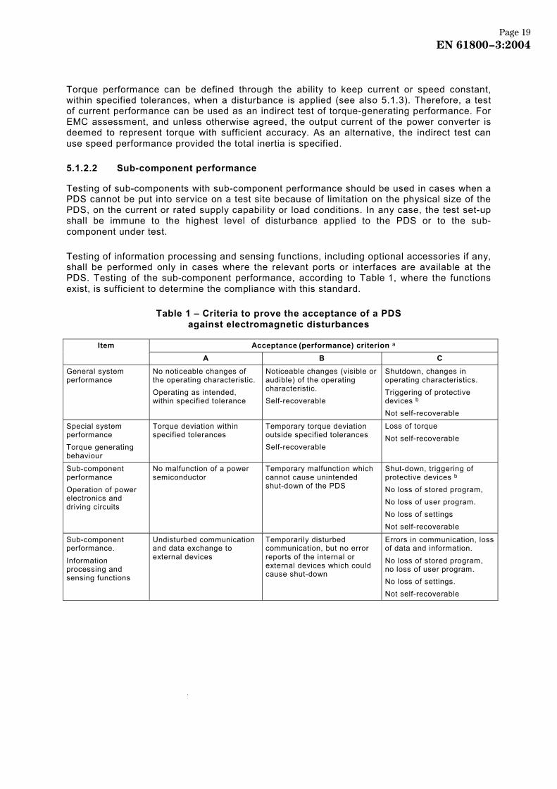
Table 1 classifies the effects of a given disturbance into three acceptance (performance) criteria: A, B and C, both for the PDS and for its sub-components.
5.1.2 Selection of performance type
5.1.2.1 General or special system performance
The “general system performance” item from Table 1 shall be defined in accordance with the special application and typical configuration of the PDS. It is the responsibility of the manufacturer to select these items.
The special system performance, torque-generating behaviour, shall be tested only in cases where it is explicitly defined in the product specification. In this case, the torque generating performance can be directly or indirectly tested. The direct test uses an EMC immune torquemeter to measure torque disturbances.
Page 18EN 61800−3:2004
Torque performance can be defined through the ability to keep current or speed constant, within specified tolerances, when a disturbance is applied (see also 5.1.3). Therefore, a test of current performance can be used as an indirect test of torque-generating performance. For EMC assessment, and unless otherwise agreed, the output current of the power converter is deemed to represent torque with sufficient accuracy. As an alternative, the indirect test can use speed performance provided the total inertia is specified.
5.1.2.2 Sub-component performance
Testing of sub-components with sub-component performance should be used in cases when a PDS cannot be put into service on a test site because of limitation on the physical size of the PDS, on the current or rated supply capability or load conditions. In any case, the test set-up shall be immune to the highest level of disturbance applied to the PDS or to the sub-component under test.
Testing of information processing and sensing functions, including optional accessories if any, shall be performed only in cases where the relevant ports or interfaces are available at the PDS. Testing of the sub-component performance, according to Table 1, where the functions exist, is sufficient to determine the compliance with this standard.
Table 1 – Criteria to prove the acceptance of a PDS against electromagnetic disturbances
Item Acceptance (performance) criterion a A B C
General system performance
No noticeable changes of the operating characteristic. Operating as intended, within specified tolerance
Noticeable changes (visible or audible) of the operating characteristic. Self-recoverable
Shutdown, changes in operating characteristics. Triggering of protective devices b
Not self-recoverable
Special system performance Torque generating behaviour
Torque deviation within specified tolerances
Temporary torque deviation outside specified tolerances Self-recoverable
Loss of torque Not self-recoverable
Sub-component performance Operation of power electronics and driving circuits
No malfunction of a power semiconductor
Temporary malfunction which cannot cause unintended shut-down of the PDS
Shut-down, triggering of protective devices b No loss of stored program, No loss of user program. No loss of settings Not self-recoverable
Sub-component performance. Information processing and sensing functions
Undisturbed communication and data exchange to external devices
Temporarily disturbed communication, but no error reports of the internal or external devices which could cause shut-down
Errors in communication, loss of data and information. No loss of stored program, no loss of user program. No loss of settings. Not self-recoverable
Page 19EN 61800−3:2004
Table 1 (continued)
Item Acceptance (performance) criterion a A B C
Sub-component performance Operation of displays and control panels
No changes of visible display information, only slight light intensity fluctuation of LEDs, or slight movement of characters
Visible temporary changes of information, undesired LED illumination
Shut down, permanent loss of information, or unpermitted operating mode, obviously wrong display information. No loss of stored program, no loss of user program. No loss of settings
a Acceptance criteria A, B, C – False starts are not acceptable. A false start is an unintended change from the logical state "STOPPED" which can make the motor run.
b Acceptance criterion C – The function can be restored by operator intervention (manual reset). Opening of fuses is allowed for line-commutated converters operating in inverting mode.
5.1.3 Conditions during the test
The load shall be within the manufacturer’s specification and the actual load shall be noted in the test report.
Testing the torque generating behaviour as well as the information processing and sensing functions requires special test equipment with adapted immunity against the parasitic coupling of the test disturbance. It can only be used if the immunity of the test set-up can be proven by reference measurements. The evaluation of the torque disturbance can be performed by a torque transducer or by measurement or calculation of the torque generating current or other indirect techniques; an adapted and immune load shall be available at the test-site.
For testing the performance of the information processing or sensing function, suitable equipment shall be available to simulate the data communication or data evaluation. This equipment shall have sufficient immunity to operate correctly during the test.
Since the motor has been tested by its manufacturer according to the relevant standards, the motor component of the PDS, with exception of the sensors, does not need any additional EMC immunity test. Therefore, while the motor is connected to the BDM/CDM for the duration of the test, EMC immunity tests on the motor itself are not required.
The tests shall be applied to the relevant ports where they exist, including those of optional accessories if any. They shall be conducted in a well-defined and reproducible manner on a port-by-port basis. However, if several process measurement and control ports or signal interfaces have the same physical configuration (layout) it is sufficient to test one port or interface of that type.
In 5.2 and 5.3 the minimum requirements, tests and acceptance criteria are stated. The acceptance criteria refer to 5.1.1.
Page 20EN 61800−3:2004
5.2 Basic immunity requirements – low-frequency disturbances
5.2.1 Common principle
The requirements in this subclause shall be used for designing the immunity of a PDS against low-frequency disturbances.
For the immunity requirements, the manufacturer may demonstrate compliance using either testing, calculation or simulation. Unless otherwise stated, it is sufficient to demonstrate that the power circuit will comply with the required acceptance criterion and that the ratings of input circuits (filters, etc.) will not be exceeded.
NOTE 1 A number of these phenomena are not required by the generic standards, but are important for the dimensioning of the power circuit of the PDS. It is difficult to test immunity against many of these phenomena, particularly when the input current exceeds 16 A or the supply voltage exceeds 400 V. However, experience of many years shows that, provided the power circuit operates correctly, the control part and the auxiliaries are generally immune. This is due to natural decoupling that exists in the PDS. Examples of such decoupling are that provided by power supplies and the time constants of auxiliary processes such as fans.
The compliance with the requirements of this part of IEC 61800 shall be stated in the user documentation. Where compliance is demonstrated by tests, the relevant basic standard in the IEC 61000-4 series may be considered (see Clause B.7).
NOTE 2 The electrical service conditions for the main and the auxiliary supply if any, are already defined in the PDS service conditions in the relevant standard IEC 61800-1 or IEC 61800-2 or IEC 61800-4. These service conditions include frequency variations, frequency rate of change, voltage variations, voltage fluctuations, voltage unbalance, harmonics and commutation notches.
NOTE 3 Possible consequences of exceeding the indicated levels (in accordance with IEC 60146-2) are:
F Functional with degradation of performance;
T Tripping or interruption of operation due to protective devices;
D Permanent damage (fuses acceptable).
Such consequences should not be regarded as an EMC concern, but as part of a safety analysis when relevant.
5.2.2 Harmonics and commutation notches/voltage distortion
5.2.2.1 Low voltage PDSs – (voltage distortion)
The PDS or BDM/CDM shall sustain the immunity levels given in Table 2. It shall be verified that these levels will not cause the ratings for the input circuits (filters, etc.) to be exceeded. Analysis of commutation notches shall be in the time domain. The manufacturer may verify immunity by calculation, simulation, or test, according to 5.2.1.
NOTE Frequency domain analysis of notches contribution to total harmonic distortion will not obviously reveal certain types of harmful effects, see Clause B.1.
Page 21EN 61800−3:2004
Table 2 – Minimum immunity requirements for harmonics and commutation notches/voltage distortion on power ports of low voltage PDSs
First environment Second environment
Phenomenon Reference document
Level Reference document
Level
Performance (acceptance)
criterion
Harmonics (THD and individual harmonic orders)
IEC 61000-2-2 Value of the compatibility level
IEC 61000-2-4
Class 3
Value of the compatibility level
A
Harmonics
short term ( < 15 s)
IEC 61000-2-2 1,5 times the value of the permanent compatibility levels
IEC 61000-2-4
Class 3
1,5 times the value of the permanent compatibility levels
B
Commutation notches
IEC 61000-1-1 No requirement IEC 60146-1-1
Class B
Depth = 40 %,
Total area = 250 in per cent degrees
A
5.2.2.2 PDSs of rated voltage above 1 000 V – (voltage distortion)
5.2.2.2.1 Main power port
The PDS or BDM/CDM shall sustain the immunity levels given in Table 3. It shall be verified that these levels will not cause the ratings for the input circuits (filters, etc.) to be exceeded. Analysis of commutation notches shall be in the time domain. The manufacturer may verify immunity by calculation, simulation, or test, according to 5.2.1.
NOTE Frequency domain analysis of notches' contribution to total harmonic distortion will not obviously reveal certain types of harmful effects, see Clause B.1.
Table 3 – Minimum immunity requirements for harmonics and commutation notches/voltage distortion on main power ports of PDSs of rated voltage above 1 000 V
Phenomenon Reference document Level Performance(acceptance)
criterion
Harmonics (THD and individual harmonic orders)
IEC 61000-2-4 Class 3
Value of the compatibility level A a
Harmonics
short term (< 15 s)
IEC 61000-2-4 Class 2
1,5 times the value of the permanent compatibility levels
A a
Interharmonics steady state IEC 61000-2-4 Class 2
Value of the compatibility level A b
Interharmonics short term (< 15 s)
IEC 61000-2-4 Class 2
1,5 times the value of the permanent compatibility levels
B a
Commutation notches IEC 60146-1-1 Depth = 40% ULWM (class B) Area c = 125 in per cent degrees (class C)
A a
a The possible consequence of exceeding the level is T (see note 3 in 5.2.1). b The possible consequence of exceeding the level is F (see note 3 in 5.2.1). c Class C of IEC 60146-1-1 is appropriate for the primary side of the transformer.
Page 22EN 61800−3:2004
5.2.2.2.2 Auxiliary power port
The auxiliary power ports of PDSs shall sustain the immunity levels given in Table 4. It shall be verified that these levels will not cause the ratings for the input circuits (filters, etc.) to be exceeded. Analysis of commutation notches shall be in the time domain. The manufacturer may verify immunity by calculation, simulation, or test, according to 5.2.1.
NOTE Frequency domain analysis of notches' contribution to total harmonic distortion will not obviously reveal certain types of harmful effects, see Clause B.1.
Table 4 – Minimum immunity requirements for harmonics and commutation notches/voltage distortion on auxiliary low voltage power ports of PDSs
Phenomenon Reference document Level Performance(acceptance)
criterion
Harmonics (THD and individual harmonic orders)
IEC 61000-2-4
Class 2
Value of the compatibility level A a
Harmonics
short term (<15 s)
IEC 61000-2-4
Class 2
1,5 times the permanent compatibility levels
A a
Commutation notches IEC 60146-1-1 Depth = 40% ULWM
Area b = 250 in per cent degrees
A a
a The possible consequence of exceeding the level is T (see note 3 in 5.2.1). b According to IEC 60146-1-1 class B.
5.2.3 Voltage deviations (variations, changes, fluctuations), dips and short
interruptions
5.2.3.1 Low voltage PDSs (voltage deviations)
The PDS or BDM/CDM shall sustain the immunity levels given in Table 5. The manufacturer may verify immunity by calculation, simulation, or test, according to 5.2.1.
Table 5 – Minimum immunity requirements for voltage deviations, dips and short interruptions on power ports of low voltage PDSs
First environment Second environment Phenomenon
Reference document
Level Reference document
Level
Performance(acceptance)
criterion
Voltage deviations IEC 61000-2-2 ±10 % IEC 61000-2-4
Class 2 ±10 % a A b
Voltage dips and short interruptions
IEC 61000-2-1 c depth 10 % to 100 %
IEC 61000-2-1 c Depth 10 % to 100 %
C d
a If class 3 of IEC 61000-2-4 is required, this should be agreed between the manufacturer and user. b When the voltage is below nominal, the maximum output power ratings – speed and/or torque – may be
reduced, because they are voltage dependent. c Typical depths and durations of voltage dips are given in 8.1.2 of IEC 61000-2-1. d Opening of fuses is allowed for line-commutated converters operating in inverting mode.
NOTE 1 A PDS is used for energy conversion and a voltage dip represents a loss of available energy. It may be necessary to trip for safety reasons, even during a voltage dip of 30 % to 50 % amplitude and 0,3 s duration.
Page 23EN 61800−3:2004
NOTE 2 A decreasing input voltage, even with few milliseconds duration, may result in blowing of fuses when applied to a line commutated thyristor converter operating under regeneration mode.
NOTE 3 The effect of a voltage dip (energy reduction) on the process cannot be defined without detailed knowledge of the process itself. This effect is a system and rating aspect, and will generally be greatest when the power demand (including losses) on the PDS is higher than the available power.
Where it is possible and not dangerous, the behaviour of the PDS during short interruptions may be verified by switching off and on the mains supply during the standard operating conditions of the PDS (see B.6.1).
The manufacturer shall state in the user documentation the degradation of performance resulting from voltage dips or short interruptions.
NOTE 4 Improvements to the immunity (use of UPS, stand-by generator, derating, etc.) may result in a considerable increase in the size and cost of the PDS and may reduce the efficiency or power factor. Operation such as automatic restart may have safety consequences, and are not covered by this standard.
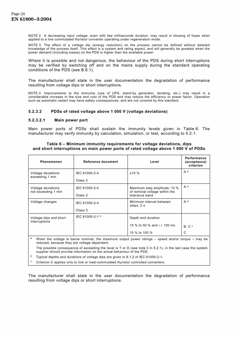
5.2.3.2 PDSs of rated voltage above 1 000 V (voltage deviations)
5.2.3.2.1 Main power port
Main power ports of PDSs shall sustain the immunity levels given in Table 6. The manufacturer may verify immunity by calculation, simulation, or test, according to 5.2.1.
Table 6 – Minimum immunity requirements for voltage deviations, dips and short interruptions on main power ports of rated voltage above 1 000 V of PDSs
Phenomenon Reference document Level Performance(acceptance)
criterion
Voltage deviations exceeding 1 min
IEC 61000-2-4
Class 3
±10 % A a
Voltage deviations not exceeding 1 min
IEC 61000-2-4
Class 3
Maximum step amplitude: 12 % of nominal voltage within the tolerance band
A a
Voltage changes IEC 61000-2-4
Class 3
Minimum interval between steps: 2 s
A a
Voltage dips and short interruptions
IEC 61000-2-1 b Depth and duration
15 % to 50 % and t ≤ 100 ms
15 % to 100 %
B, C c
C a When the voltage is below nominal, the maximum output power ratings – speed and/or torque – may be
reduced, because they are voltage dependent. The possible consequence of exceeding the level is T or D (see note 3 in 5.2.1), in the last case the system
supplier should provide information on the actual behaviour of the PDS. b Typical depths and durations of voltage dips are given in 8.1.2 of IEC 61000-2-1. c Criterion C applies only to line or load-commutated thyristor controlled converters.
The manufacturer shall state in the user documentation the degradation of performance resulting from voltage dips or short interruptions.
Page 24EN 61800−3:2004
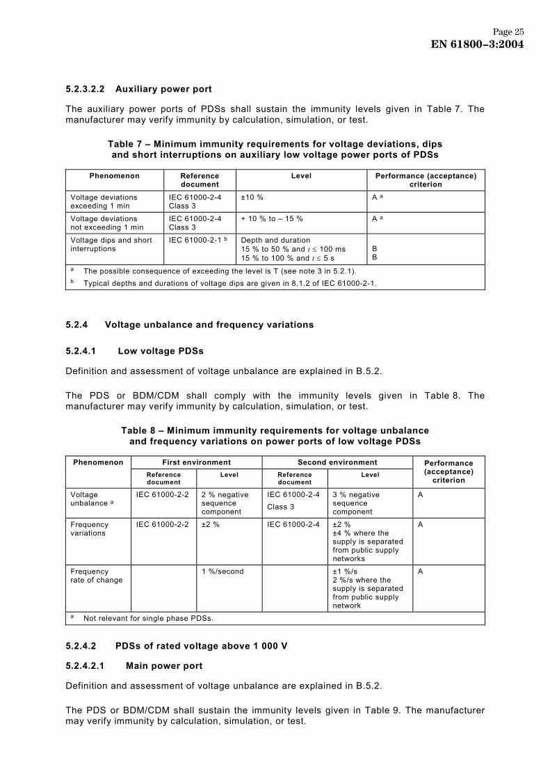
5.2.3.2.2 Auxiliary power port
The auxiliary power ports of PDSs shall sustain the immunity levels given in Table 7. The manufacturer may verify immunity by calculation, simulation, or test.
Table 7 – Minimum immunity requirements for voltage deviations, dips and short interruptions on auxiliary low voltage power ports of PDSs
Phenomenon Reference document
Level Performance (acceptance)criterion
Voltage deviations exceeding 1 min
IEC 61000-2-4 Class 3
±10 % A a
Voltage deviations not exceeding 1 min
IEC 61000-2-4 Class 3
+ 10 % to – 15 % A a
Voltage dips and short interruptions
IEC 61000-2-1 b Depth and duration 15 % to 50 % and t ≤ 100 ms 15 % to 100 % and t ≤ 5 s
B B
a The possible consequence of exceeding the level is T (see note 3 in 5.2.1). b Typical depths and durations of voltage dips are given in 8.1.2 of IEC 61000-2-1.
5.2.4 Voltage unbalance and frequency variations
5.2.4.1 Low voltage PDSs
Definition and assessment of voltage unbalance are explained in B.5.2.
The PDS or BDM/CDM shall comply with the immunity levels given in Table 8. The manufacturer may verify immunity by calculation, simulation, or test.
Table 8 – Minimum immunity requirements for voltage unbalance and frequency variations on power ports of low voltage PDSs
First environment Second environment Phenomenon Reference document
Level Reference document
Level Performance (acceptance)
criterion
Voltage unbalance a
IEC 61000-2-2 2 % negative sequence component
IEC 61000-2-4 Class 3
3 % negative sequence component
A
Frequency variations
IEC 61000-2-2 ±2 % IEC 61000-2-4 ±2 % ±4 % where the supply is separated from public supply networks
A
Frequency rate of change
1 %/second ±1 %/s 2 %/s where the supply is separated from public supply network
A
a Not relevant for single phase PDSs.
5.2.4.2 PDSs of rated voltage above 1 000 V
5.2.4.2.1 Main power port
Definition and assessment of voltage unbalance are explained in B.5.2.
The PDS or BDM/CDM shall sustain the immunity levels given in Table 9. The manufacturer may verify immunity by calculation, simulation, or test.
Page 25EN 61800−3:2004
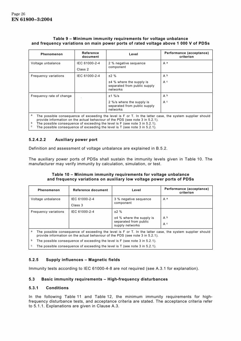
Table 9 – Minimum immunity requirements for voltage unbalance and frequency variations on main power ports of rated voltage above 1 000 V of PDSs
Phenomenon Reference document
Level Performance (acceptance)criterion
Voltage unbalance IEC 61000-2-4
Class 2
2 % negative sequence component
A a
Frequency variations IEC 61000-2-4 ±2 %
±4 % where the supply is separated from public supply networks
A b
A c
Frequency rate of change ±1 %/s
2 %/s where the supply is separated from public supply networks
A b
A c
a The possible consequence of exceeding the level is F or T. In the latter case, the system supplier should provide information on the actual behaviour of the PDS (see note 3 in 5.2.1).
b The possible consequence of exceeding the level is F (see note 3 in 5.2.1). c The possible consequence of exceeding the level is T (see note 3 in 5.2.1).
5.2.4.2.2 Auxiliary power port
Definition and assessment of voltage unbalance are explained in B.5.2.
The auxiliary power ports of PDSs shall sustain the immunity levels given in Table 10. The manufacturer may verify immunity by calculation, simulation, or test.
Table 10 – Minimum immunity requirements for voltage unbalance and frequency variations on auxiliary low voltage power ports of PDSs
Phenomenon Reference document Level Performance (acceptance)criterion
Voltage unbalance IEC 61000-2-4
Class 3
3 % negative sequence component
A a
Frequency variations IEC 61000-2-4 ±2 %
±4 % where the supply is separated from public supply networks
A b
A c
a The possible consequence of exceeding the level is F or T. In the latter case, the system supplier should provide information on the actual behaviour of the PDS (see note 3 in 5.2.1).
b The possible consequence of exceeding the level is F (see note 3 in 5.2.1). c The possible consequence of exceeding the level is T (see note 3 in 5.2.1).
5.2.5 Supply influences – Magnetic fields
Immunity tests according to IEC 61000-4-8 are not required (see A.3.1 for explanation).
5.3 Basic immunity requirements – High-frequency disturbances
5.3.1 Conditions
In the following Table 11 and Table 12, the minimum immunity requirements for high-frequency disturbance tests, and acceptance criteria are stated. The acceptance criteria refer to 5.1.1. Explanations are given in Clause A.3.
Page 26EN 61800−3:2004
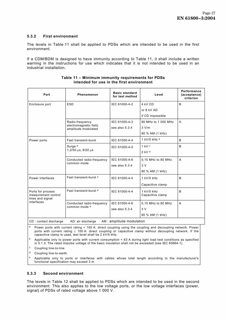
5.3.2 First environment
The levels in Table 11 shall be applied to PDSs which are intended to be used in the first environment.
If a CDM/BDM is designed to have immunity according to Table 11, it shall include a written warning in the instructions for use which indicates that it is not intended to be used in an industrial installation.
Table 11 – Minimum immunity requirements for PDSs intended for use in the first environment
Port Phenomenon Basic standard for test method Level
Performance(acceptance)
criterion
ESD IEC 61000-4-2 4 kV CD
or 8 kV AD
if CD impossible
B Enclosure port
Radio-frequency electromagnetic field, amplitude modulated
IEC 61000-4-3
see also 5.3.4
80 MHz to 1 000 MHz
3 V/m
80 % AM (1 kHz)
A
Fast transient-burst IEC 61000-4-4 1 kV/5 kHz a B
Surge b 1,2/50 µs, 8/20 µs
IEC 61000-4-5
1 kV c
2 kV d
B
Power ports
Conducted radio-frequency common mode
IEC 61000-4-6
see also 5.3.4
0,15 MHz to 80 MHz
3 V
80 % AM (1 kHz)
A
Power interfaces Fast transient-burst e IEC 61000-4-4 1 kV/5 kHz
Capacitive clamp
B
Fast transient-burst e IEC 61000-4-4
1 kV/5 kHz Capacitive clamp
B Ports for process measurement control lines and signal interfaces Conducted radio-frequency
common mode e IEC 61000-4-6
see also 5.3.4
0,15 MHz to 80 MHz
3 V
80 % AM (1 kHz)
A
CD : contact discharge AD: air discharge AM : amplitude modulation a Power ports with current rating < 100 A: direct coupling using the coupling and decoupling network. Power
ports with current rating ≥ 100 A: direct coupling or capacitive clamp without decoupling network. If the capacitive clamp is used, test level shall be 2 kV/5 kHz.
b Applicable only to power ports with current consumption < 63 A during light load test conditions as specified in 5.1.3. The rated impulse voltage of the basic insulation shall not be exceeded (see IEC 60664-1).
c Coupling line-to-line. d Coupling line-to-earth. e Applicable only to ports or interfaces with cables whose total length according to the manufacturer's
functional specification may exceed 3 m.
5.3.3 Second environment
The levels in Table 12 shall be applied to PDSs which are intended to be used in the second environment. This also applies to the low voltage ports, or the low voltage interfaces (power, signal) of PDSs of rated voltage above 1 000 V.
Page 27EN 61800−3:2004
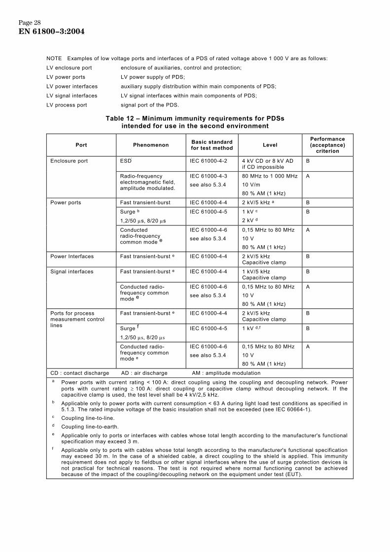
NOTE Examples of low voltage ports and interfaces of a PDS of rated voltage above 1 000 V are as follows:
LV enclosure port enclosure of auxiliaries, control and protection;
LV power ports LV power supply of PDS;
LV power interfaces auxiliary supply distribution within main components of PDS;
LV signal interfaces LV signal interfaces within main components of PDS;
LV process port signal port of the PDS.
Table 12 – Minimum immunity requirements for PDSs intended for use in the second environment
Port Phenomenon Basic standard for test method Level
Performance (acceptance)
criterion
ESD IEC 61000-4-2 4 kV CD or 8 kV AD
if CD impossible B Enclosure port
Radio-frequency electromagnetic field, amplitude modulated.
IEC 61000-4-3 see also 5.3.4
80 MHz to 1 000 MHz 10 V/m 80 % AM (1 kHz)
A
Fast transient-burst IEC 61000-4-4 2 kV/5 kHz a B
Surge b
1,2/50 µs, 8/20 µs
IEC 61000-4-5 1 kV c 2 kV d
B
Power ports
Conducted radio-frequency common mode e
IEC 61000-4-6 see also 5.3.4
0,15 MHz to 80 MHz 10 V 80 % AM (1 kHz)
A
Power Interfaces Fast transient-burst e IEC 61000-4-4 2 kV/5 kHz Capacitive clamp
B
Fast transient-burst e IEC 61000-4-4 1 kV/5 kHz Capacitive clamp
B Signal interfaces
Conducted radio-frequency common mode e
IEC 61000-4-6 see also 5.3.4
0,15 MHz to 80 MHz 10 V 80 % AM (1 kHz)
A
Fast transient-burst e IEC 61000-4-4 2 kV/5 kHz Capacitive clamp
B
Surge f
1,2/50 µs, 8/20 µs
IEC 61000-4-5 1 kV d,f B
Ports for process measurement control lines
Conducted radio-frequency common mode e
IEC 61000-4-6 see also 5.3.4
0,15 MHz to 80 MHz 10 V 80 % AM (1 kHz)
A
CD : contact discharge AD : air discharge AM : amplitude modulation a Power ports with current rating < 100 A: direct coupling using the coupling and decoupling network. Power
ports with current rating ≥ 100 A: direct coupling or capacitive clamp without decoupling network. If the capacitive clamp is used, the test level shall be 4 kV/2,5 kHz.
b Applicable only to power ports with current consumption < 63 A during light load test conditions as specified in 5.1.3. The rated impulse voltage of the basic insulation shall not be exceeded (see IEC 60664-1).
c Coupling line-to-line. d Coupling line-to-earth. e Applicable only to ports or interfaces with cables whose total length according to the manufacturer's functional
specification may exceed 3 m. f Applicable only to ports with cables whose total length according to the manufacturer's functional specification
may exceed 30 m. In the case of a shielded cable, a direct coupling to the shield is applied. This immunity requirement does not apply to fieldbus or other signal interfaces where the use of surge protection devices is not practical for technical reasons. The test is not required where normal functioning cannot be achieved because of the impact of the coupling/decoupling network on the equipment under test (EUT).
Page 28EN 61800−3:2004
These phenomena are not relevant for application to the ports of rated insulation voltage above 1 000 V. For simplicity, such ports are named HV ports of PDSs of rated voltage above 1 000 V.
NOTE Examples of HV ports and interfaces of a PDS of rated voltage above 1 000 V are as follows:
HV enclosure port enclosure of transformer, converter section and motor;
HV power port primary side of transformer;
HV power interfaces HV distribution within main components of PDS;
HV signal interfaces HV signal interfaces within main components of PDS.
5.3.4 Immunity against electromagnetic fields
If the PDS is:
– of rated voltage not more than 500 V; – of rated current not more than 200 A; – of total mass not more than 250 kg, and – of height, width, and depth not more than 1,9 m,
the tests of IEC 61000-4-3 and IEC 61000-4-6 shall be performed, see 5.3.2 and 5.3.3.
If the PDS is larger or of higher rating than in the above paragraph then the manufacturer shall choose either:
– to perform the tests of IEC 61000-4-3 and IEC 61000-4-6 on the PDS or – to perform the tests of IEC 61000-4-3 and IEC 61000-4-6 on sensitive sub-components.
If the motor is too large to be put into service on a test site, the motor may be replaced by one of smaller size, provided this does not adversely affect the operation of the CDM/BDM.
In the case where only sub-components have been tested, a test against radio-communication devices of common industrial use should be performed on the complete PDS, as described in A.3.2.2. This test is only valid for the specific location, installed equipment and frequencies tested.
5.4 Application of immunity requirements – statistical aspect
When choosing the acceptance level for a specific test of a PDS, it shall be understood that the test result implies only a probability of performance. Depending on the acceptance criterion and the application of a PDS, this probability shall be considered in specifying the number of test pulses or duration of the test.
Immunity requirements in 5.3 shall be verified by performing a type-test on a representative unit. The manufacturer or supplier shall ensure the EMC performance of the product is maintained in production by using some form of quality control.
Measurement results obtained for a PDS while installed in its place of use (not on a test site) shall relate to that installation only.
Page 29EN 61800−3:2004
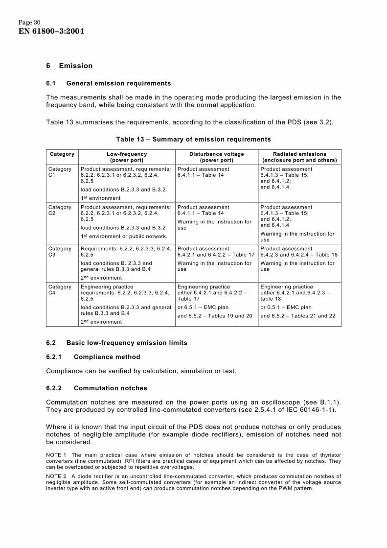
6 Emission
6.1 General emission requirements
The measurements shall be made in the operating mode producing the largest emission in the frequency band, while being consistent with the normal application.
Table 13 summarises the requirements, according to the classification of the PDS (see 3.2).
Table 13 – Summary of emission requirements
Category Low-frequency (power port)
Disturbance voltage (power port)
Radiated emissions (enclosure port and others)
Category C1
Product assessment, requirements: 6.2.2, 6.2.3.1 or 6.2.3.2, 6.2.4, 6.2.5 load conditions B.2.3.3 and B.3.2. 1st environment
Product assessment 6.4.1.1 – Table 14
Product assessment 6.4.1.3 – Table 15; and 6.4.1.2; and 6.4.1.4.
Category C2
Product assessment, requirements: 6.2.2, 6.2.3.1 or 6.2.3.2, 6.2.4, 6.2.5 load conditions B.2.3.3 and B.3.2 1st environment or public network.
Product assessment 6.4.1.1 – Table 14 Warning in the instruction for use
Product assessment 6.4.1.3 – Table 15; and 6.4.1.2; and 6.4.1.4 Warning in the instruction for use
Category C3
Requirements: 6.2.2, 6.2.3.3, 6.2.4, 6.2.5 load conditions B. 2.3.3 and general rules B.3.3 and B.4 2nd environment
Product assessment 6.4.2.1 and 6.4.2.2 – Table 17 Warning in the instruction for use
Product assessment 6.4.2.3 and 6.4.2.4 – Table 18 Warning in the instruction for use
Category C4
Engineering practice requirements: 6.2.2, 6.2.3.3, 6.2.4, 6.2.5 load conditions B.2.3.3 and general rules B.3.3 and B.4 2nd environment
Engineering practice either 6.4.2.1 and 6.4.2.2 – Table 17 or 6.5.1 – EMC plan and 6.5.2 – Tables 19 and 20
Engineering practice either 6.4.2.1 and.6.4.2.3 – table 18 or 6.5.1 – EMC plan and 6.5.2 – Tables 21 and 22
6.2 Basic low-frequency emission limits
6.2.1 Compliance method
Compliance can be verified by calculation, simulation or test.
6.2.2 Commutation notches
Commutation notches are measured on the power ports using an oscilloscope (see B.1.1). They are produced by controlled line-commutated converters (see 2.5.4.1 of IEC 60146-1-1).
Where it is known that the input circuit of the PDS does not produce notches or only produces notches of negligible amplitude (for example diode rectifiers), emission of notches need not be considered.
NOTE 1 The main practical case where emission of notches should be considered is the case of thyristor converters (line commutated). RFI filters are practical cases of equipment which can be affected by notches. They can be overloaded or subjected to repetitive overvoltages.
NOTE 2 A diode rectifier is an uncontrolled line-commutated converter, which produces commutation notches of negligible amplitude. Some self-commutated converters (for example an indirect converter of the voltage source inverter type with an active front end) can produce commutation notches depending on the PWM pattern.
Page 30EN 61800−3:2004
Where notches are to be considered, the manufacturer shall provide the following information to the user:
– value of any decoupling reactances which are included in the PDS; – available decoupling reactances which can be externally added for mitigation (see B.1.2).
The recommendations of B.1.3 should be followed.
6.2.3 Harmonics and interharmonics
6.2.3.1 Low-voltage public supply network – Equipment covered by IEC 61000-3-2
Equipment may contain one or several PDSs and also other loads.
When a PDS is an equipment within the scope of IEC 61000-3-2, the requirements of that standard apply. However, when one or more PDSs are included in equipment within the scope of IEC 61000-3-2, the requirements of that standard apply to the complete equipment and not to the individual PDS. It is the responsibility of the equipment manufacturer to define the boundary of the system or sub-system to which IEC 61000-3-2 applies, and the method which demonstrates compliance of the equipment.
6.2.3.2 Low-voltage public supply network – Equipment not covered by IEC 61000-3-2
For equipment not covered by IEC 61000-3-2, (example: rated current above 16 A) recommendations may be found in the technical report IEC 61000-3-4 and in Clause B.4. Where, for technical or economic reasons as explained in Annexes B and C of this standard, stage 1 or stage 2 of IEC 61000-3-4 cannot be applied, the approach of stage 3 is facilitated by Annex B.
The manufacturer shall provide in the documentation of the PDS, or on request, the current harmonic level, under rated load conditions, as a percentage of the rated fundamental current on the power port. These may be produced by calculation, simulation or test.
For the purpose of calculation or simulation, the applied voltage shall be assumed to have a THD less than 1 %. The internal impedance of the network shall be assumed to be purely inductive. If the specific location of the PDS is not known, the harmonic currents shall be calculated assuming that the PDS is connected to a PC with the highest value of RSI permitted by the PDS manufacturer.
LN
SCSI I
IR =
where ISC is the short circuit current at the considered PC, ILN is the rated input current of the PDS.
If the manufacturer does not state a maximum value of RSI, a value of 250 shall be assumed. If the specific location of the PDS is known, the supply impedance at that location should be used.
The PDS manufacturer shall calculate the harmonic currents for each order up to the 40th. The current THD (orders up to and including 40) shall also be calculated.
Page 31EN 61800−3:2004
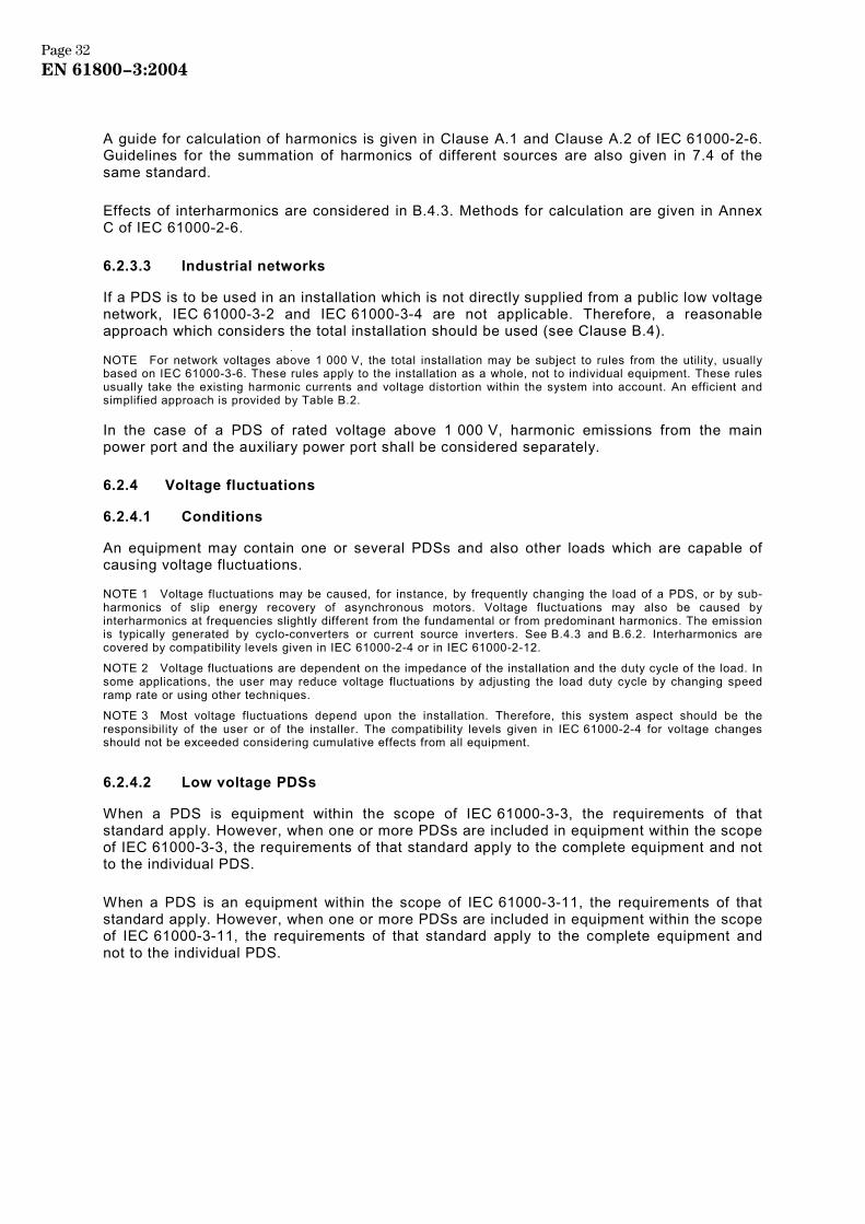
A guide for calculation of harmonics is given in Clause A.1 and Clause A.2 of IEC 61000-2-6. Guidelines for the summation of harmonics of different sources are also given in 7.4 of the same standard.
Effects of interharmonics are considered in B.4.3. Methods for calculation are given in Annex C of IEC 61000-2-6.
6.2.3.3 Industrial networks
If a PDS is to be used in an installation which is not directly supplied from a public low voltage network, IEC 61000-3-2 and IEC 61000-3-4 are not applicable. Therefore, a reasonable approach which considers the total installation should be used (see Clause B.4).
NOTE For network voltages above 1 000 V, the total installation may be subject to rules from the utility, usually based on IEC 61000-3-6. These rules apply to the installation as a whole, not to individual equipment. These rules usually take the existing harmonic currents and voltage distortion within the system into account. An efficient and simplified approach is provided by Table B.2.
In the case of a PDS of rated voltage above 1 000 V, harmonic emissions from the main power port and the auxiliary power port shall be considered separately.
6.2.4 Voltage fluctuations
6.2.4.1 Conditions
An equipment may contain one or several PDSs and also other loads which are capable of causing voltage fluctuations.
NOTE 1 Voltage fluctuations may be caused, for instance, by frequently changing the load of a PDS, or by sub-harmonics of slip energy recovery of asynchronous motors. Voltage fluctuations may also be caused by interharmonics at frequencies slightly different from the fundamental or from predominant harmonics. The emission is typically generated by cyclo-converters or current source inverters. See B.4.3 and B.6.2. Interharmonics are covered by compatibility levels given in IEC 61000-2-4 or in IEC 61000-2-12.
NOTE 2 Voltage fluctuations are dependent on the impedance of the installation and the duty cycle of the load. In some applications, the user may reduce voltage fluctuations by adjusting the load duty cycle by changing speed ramp rate or using other techniques. NOTE 3 Most voltage fluctuations depend upon the installation. Therefore, this system aspect should be the responsibility of the user or of the installer. The compatibility levels given in IEC 61000-2-4 for voltage changes should not be exceeded considering cumulative effects from all equipment.
6.2.4.2 Low voltage PDSs
When a PDS is equipment within the scope of IEC 61000-3-3, the requirements of that standard apply. However, when one or more PDSs are included in equipment within the scope of IEC 61000-3-3, the requirements of that standard apply to the complete equipment and not to the individual PDS.
When a PDS is an equipment within the scope of IEC 61000-3-11, the requirements of that standard apply. However, when one or more PDSs are included in equipment within the scope of IEC 61000-3-11, the requirements of that standard apply to the complete equipment and not to the individual PDS.
Page 32EN 61800−3:2004
6.2.4.3 PDSs of rated voltage above 1 000 V
The technical report IEC 61000-3-7 applies to the total installation considering all circuits on the load side of the PCC. Application of this report generally results in local rules from the utility. Compliance with the rules requires the assessment of total fluctuation emission of the total installation to which the considered PDS contributes.
NOTE Most voltage fluctuations are relevant to the installation. Therefore, this system aspect should be the responsibility of the user or of the installer. The compatibility levels given in IEC 61000-2-12 for voltage changes should not be exceeded considering cumulative effects from all equipment.
6.2.5 Common mode harmonic emission (low-frequency common mode voltage)
The switching frequency of the converter of the PDS is often in the audible frequency range and, in particular, the frequency range commonly used by telephone and data systems. To avoid the risk of crosstalk to signal cables, the installation instructions shall either recommend that the power interface cable be segregated from signal cables or state alternative mitigation methods.
6.3 Conditions related to high-frequency emission measurement
6.3.1 General requirements
6.3.1.1 Common conditions
The rate of change of voltage or current is expected to be the main source of high-frequency emission. For this type of emission the dv/dt values of the PDS are mostly relevant and these can be achieved with output currents lower than the rated current of the PDS. Therefore, these tests are light load tests. The tests shall be applied to the relevant ports where they exist and shall be performed in a well-defined and reproducible manner on a port-by-port basis. The test method shall comply with 6.2 to 6.4 and clause 7 of CISPR 11, paying particular attention to earth connections.
The load shall be within the manufacturer’s specification and the actual load shall be noted in the test report.
6.3.1.2 Conducted emissions
The measurement equipment for evaluation of high-frequency mains terminal (power port) disturbance voltage emission is either the artificial mains network (50 Ω/50 µH, see CISPR 16-1 and CISPR 11) where it can be applied, or the voltage probe according to CISPR 16-1, where the artificial mains network is not applicable.
For in situ measurement of the mains disturbance voltage, a voltage probe without an artificial mains network shall be used (see 6.2.3 of CISPR 11). The same can be applied if the PDS has an input current greater than 100 A, or if the input voltage is greater than or equal to 500 V, or if the PDS contains a line commutated converter (see A.4.1.2).
6.3.1.3 Radiated emissions
Equipment of category C1 and category C2 shall be measured on a test site compliant with requirements of CISPR 16-1.
Page 33EN 61800−3:2004
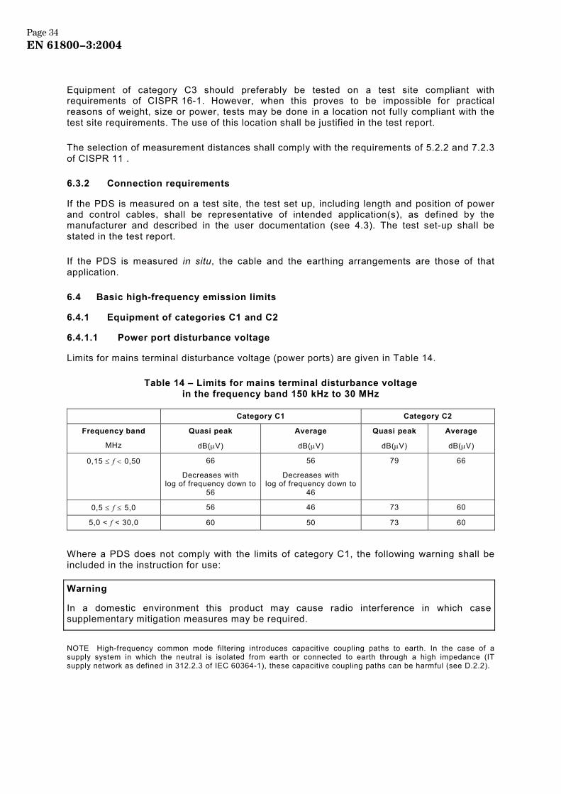
Equipment of category C3 should preferably be tested on a test site compliant with requirements of CISPR 16-1. However, when this proves to be impossible for practical reasons of weight, size or power, tests may be done in a location not fully compliant with the test site requirements. The use of this location shall be justified in the test report.
The selection of measurement distances shall comply with the requirements of 5.2.2 and 7.2.3 of CISPR 11 .
6.3.2 Connection requirements
If the PDS is measured on a test site, the test set up, including length and position of power and control cables, shall be representative of intended application(s), as defined by the manufacturer and described in the user documentation (see 4.3). The test set-up shall be stated in the test report.
If the PDS is measured in situ, the cable and the earthing arrangements are those of that application.
6.4 Basic high-frequency emission limits
6.4.1 Equipment of categories C1 and C2
6.4.1.1 Power port disturbance voltage
Limits for mains terminal disturbance voltage (power ports) are given in Table 14.
Table 14 – Limits for mains terminal disturbance voltage in the frequency band 150 kHz to 30 MHz
Category C1 Category C2
Frequency band
MHz
Quasi peak
dB(µV)
Average
dB(µV)
Quasi peak
dB(µV)
Average
dB(µV)
0,15 ≤ f < 0,50 66
Decreases with log of frequency down to
56
56
Decreases with log of frequency down to
46
79 66
0,5 ≤ f ≤ 5,0 56 46 73 60
5,0 < f < 30,0 60 50 73 60
Where a PDS does not comply with the limits of category C1, the following warning shall be included in the instruction for use:
Warning
In a domestic environment this product may cause radio interference in which case supplementary mitigation measures may be required.
NOTE High-frequency common mode filtering introduces capacitive coupling paths to earth. In the case of a supply system in which the neutral is isolated from earth or connected to earth through a high impedance (IT supply network as defined in 312.2.3 of IEC 60364-1), these capacitive coupling paths can be harmful (see D.2.2).
Page 34EN 61800−3:2004
6.4.1.2 Process measurement and control ports
If a process measurement and control port is intended for connection to a fieldbus, then the port shall comply with the conducted emission requirements of the relevant standard for that fieldbus.
If a process measurement and control port is intended for connection to a public telecommunication network, then this port shall be regarded as a telecommunication port. The conducted emission requirements of CISPR 22, class B apply to that port.
6.4.1.3 Radiation – Enclosure port
Limits for electromagnetic radiation disturbance (enclosure port, see definition in 3.3.4 and Figure 2) are given in Table 15.
Table 15 – Limits for electromagnetic radiation disturbance in the frequency band 30 MHz to 1 000 MHz
Category C1 Category C2 Frequency band
MHz Electric field strength component
Quasi-peak dB(µV/m)
Electric field strength component Quasi-peak dB(µV/m)
30 ≤ f ≤ 230
230 < f ≤ 1 000
30
37
40
47
NOTE Measurement distance 10 m.
For category C1, if the field strength measurement at 10 m cannot be made because of high ambient noise levels or for other reasons, measurement may be made at 3 m. If the 3 m distance is used, the measurement result obtained shall be normalised to 10 m by subtracting 10 dB from the result. In this case, care should be taken to avoid near field effects, particularly when the PDS is not of an appropriately small size, and at frequencies near 30 MHz.
Where a PDS does not comply with the limits of category C1, the following warning shall be included in the instructions for use:
Warning
In a domestic environment, this product may cause radio interference, in which case supplementary mitigation measures may be required.
6.4.1.4 Power interface emission
For a PDS to be operated in the first environment, the limitation of emission shall be provided by means of one of the following options.
a) Measurements on the power interface need not be performed if the length of the corresponding cable is less than 2 m, or if a shielded cable is used. The shielding shall then be of high frequency quality, continuous throughout its length and at least connected to the CDM and motor via 360° terminations.
b) The emission shall be checked by measuring the disturbance voltage at the power interface in the BDM, according to CISPR 14 and applying the limits given in Table 16.
Page 35EN 61800−3:2004
c) Where mitigation methods applied are not suitable for checking according to item b) (for example common mode mitigation methods), the effectiveness of the mitigation method shall be checked by establishing a coupling between the mains input cable and the motor cable during the measurement of the mains terminal disturbance voltage according to 6.4.1.1. This coupling shall be established over the 1 m distance separating the EUT and the AMN by running the motor cable parallel to the mains cable with a separation not exceeding 10 cm over a length of at least 0,60 m.
Table 16 – Limits of disturbance voltage on the power interface
Measurement at rated output current Frequency band
MHz Quasi peak dB(µV)
Average dB(µV)
0,15 ≤ f < 0,5 80 70
0,50 ≤ f < 30 74 64
6.4.2 Equipment of category C3
6.4.2.1 Information requirement
If a PDS does not meet the limits of category C1 or C2, a warning shall be included in the instructions for use stating that:
– this type of PDS is not intended to be used on a low-voltage public network which supplies domestic premises;
– radio frequency interference is expected if used on such a network.
The manufacturer shall provide a guide for installation and use, including recommended mitigation devices.
6.4.2.2 Power port disturbance voltage
Limits for mains terminal disturbance voltage (power ports) of PDSs are given in Table 17. The same limits apply to low voltage power ports of PDSs of rated voltage above 1 000 V.
Table 17 – Limits for mains terminal disturbance voltage in the frequency band 150 kHz to 30 MHz
PDS in the second environment – PDS of category C3
Size of PDS a Frequency band MHz
Quasi peak dB(µV)
Average dB(µV)
I ≤ 100 A
0,15 ≤ f < 0,50
0,5 ≤ f < 5,0
5,0 ≤ f < 30,0
100
86
90
Decreases with log of frequency down to 70
90
76
80
Decreases with log of frequency down to 60
100 A < I
0,15 ≤ f < 0,50
0,5 ≤ f < 5,0
5,0 ≤ f < 30,0
130
125
115
120
115
105
These limits do not apply to power ports operating above 1 000 V. a Size of the PDS refers to rated current (I) of the port.
See also clause D.2.
Page 36EN 61800−3:2004
For PDS above 100 A without dedicated transformer, to avoid the risk of crosstalk to signal cables, the installation instructions shall either recommend that the power cables be segregated from signal cables or state alternative mitigation methods.
6.4.2.3 Process measurement and control ports
If a process measurement and control port is intended for connection to a fieldbus, then the port shall comply with the conducted emission requirements of the relevant standard for that fieldbus.
If a process measurement and control port is intended for connection to a public telecommunication network, then this port shall be regarded as a telecommunication port. The conducted emission requirements of CISPR 22 class A apply to that port.
6.4.2.4 Radiation – Enclosure port
Limits for electromagnetic radiation disturbance (enclosure port, see definition in 3.3.4 and Figure 2) of PDSs are given in Table 18.
Table 18 – Limits for electromagnetic radiation disturbance in the frequency band 30 MHz to 1 000 MHz
PDS in the second environment – PDS of category C3
Frequency band MHz
Quasi peak limits dB(µV/m)
30 ≤ f ≤ 230
230 < f ≤ 1 000
50
60
NOTE Measuring distance 10 m.
NOTE This table will be reconsidered in the future according to the work which is ongoing in CISPR/B.
6.4.2.5 Power interface
For a PDS to be operated in the second environment, the instructions for installation and use shall contain all the necessary information on the installation of the power interface as required in 4.3.
6.5 Engineering practice
6.5.1 PDS of category C4
For PDSs of category C4, the following procedure shall be used.
General conditions. Due to technical reasons, there are some applications where it is not possible for the PDS to comply with the limits of Table 17 and Table 18. These applications are for large ratings or to meet specific technical requirements:
– voltage above 1 000 V; – current above 400 A; – networks isolated from earth, or connected to earth through a high impedance (IT system
according to 312.2.3 of IEC 60364-1); – where required dynamic performances will be limited as a result of filtering.
Page 37EN 61800−3:2004
In these applications of category C4 equipment, the user and the manufacturer shall agree on an EMC plan to meet the EMC requirements of the intended application (see annex E). In this situation, the user defines the EMC characteristics of the environment including the whole installation and the neighbourhood (see Figure 5). The manufacturer shall provide information on typical emission levels of the PDS which is to be installed. In the case of interference, the requirements and the procedure in 6.5.2 shall be applied.
NOTE Examples of common mitigation methods resulting from the EMC plan are: global filtering, dedicated special transformer, separation of cables, etc.
Filtering in IT-network. The use of filtered PDSs in an isolated, or high impedance earthed industrial distribution network may cause a safety risk, if not properly designed for these applications. In the case of IT networks for complex industrial systems, limits cannot be set. The diversity of solutions resulting from the knowledge of the system cannot be standardised. The main considerations are related to fault conditions and filter leakage current.
a) Short circuit to earth on the motor side of the PDS. This can cause a trip of the IT monitoring system which will lead to an undesired process shut down.
b) Short circuit to earth on the motor side can cause the application of common mode voltage to other neighbouring equipment.
c) An undesired fail detection by the IT monitoring system because of increased capacitance to earth, which will lead to an undesired process shut down.
The solutions are based on a case by case analysis.
6.5.2 Limits outside the boundary of an installation, for a PDS of category C4 – Example of propagation of disturbances
6.5.2.1 General
For PDSs in the second environment, the user shall ensure that excessive disturbances are not induced into neighbouring low-voltage networks, even if propagation is through a medium-voltage network.
In the case of complaints about interference occurring at a neighbouring low-voltage network, or in the case of a dispute between the user of a PDS (for example within installation 2 – see Figure 5), and a victim on another network (for example within installation 1), it shall first be clearly established that the disturbance of victim equipment (in installation 1) occurs when the supposed emitting PDS (installation 2) is operated.
6.5.2.2 Interference due to conduction
In this case, the measurements shall be carried out at the low-voltage secondary of the medium-voltage transformer of the installation (installation 1) where the victim is situated (see Figure 5 for point of measurement). The requirements given by Table 19 or Table 20 and Table 21 including the reservations concerning ambient noise, shall be fulfilled.
Page 38EN 61800−3:2004
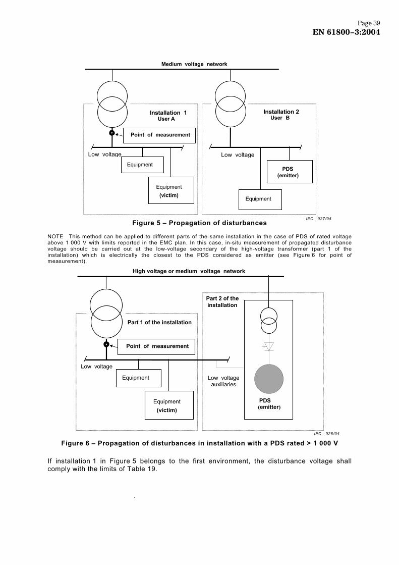
Point of measurement
Low voltageEquipment
Equipment(victim)
Installation 1User A
Low voltage
Installation 2User B
Equipment
PDS(emitter)
Medium voltage network
Figure 5 – Propagation of disturbances
NOTE This method can be applied to different parts of the same installation in the case of PDS of rated voltage above 1 000 V with limits reported in the EMC plan. In this case, in-situ measurement of propagated disturbance voltage should be carried out at the low-voltage secondary of the high-voltage transformer (part 1 of the installation) which is electrically the closest to the PDS considered as emitter (see Figure 6 for point of measurement).
Point of measurement
Low voltage
Equipment
Equipment(victim)
Part 1 of the installation
Low voltageauxiliaries
Part 2 of theinstallation
PDS(emitter)
High voltage or medium voltage network
Figure 6 – Propagation of disturbances in installation with a PDS rated > 1 000 V
If installation 1 in Figure 5 belongs to the first environment, the disturbance voltage shall comply with the limits of Table 19.
IEC 927/04
IEC 928/04
Page 39EN 61800−3:2004
Table 19 – Limits for propagated disturbance voltage ("outside" in the first environment)
Frequency band MHz
Quasi peak dB(µV)
Average dB(µV)
0,15 ≤ f < 0,50 66 Decreases with log. of frequency
down to 56
56 Decrease with log. of frequency
down to 46
0,5 ≤ f ≤ 5,0 56 46
5,0 < f < 30,0 60 50
If installation 1 in Figure 5 or part 1 of the installation in Figure 6 belongs to the second environment, the disturbance voltage shall comply with the limits of Table 20.
Table 20 – Limits for propagated disturbance voltage ("outside" in the second environment)
Frequency band MHz
Quasi peak dB(µV)
Average dB(µV)
0,15 ≤ f < 0,50 79 66
0,5 ≤ f ≤ 5,0 73 60
5,0 < f < 30,0 73 60
If the ambient noise (without operation of the PDS which is the supposed emitter) exceeds the limits (Table 19 and Table 20), the supposed emitting PDS is only considered to fail if a characteristic set of emitted frequencies can be recognised and exceeds the measured ambient noise.
6.5.2.3 Interference due to radiation
6.5.2.3.1 Radiation above 30 MHz
In case of interference, the radiation shall be measured at a distance of 10 m from the boundary of the installation, if interference occurs outside in the first environment, or at a distance of 30 m from the boundary of the installation, if interference occurs outside in the second environment. The measured field strength shall comply with Table 21.
Table 21 – Limits for propagated electromagnetic disturbance above 30 MHz
Frequency band MHz
Electric field strength component Quasi peak
dB(µV/m)
30 ≤ f ≤ 230 30
230 < f ≤ 1 000 37
If the ambient noise (without operation of the PDS which is the supposed emitter) exceeds the limits (Table 21), the supposed emitting PDS is only considered to fail if a characteristic set of emitted frequencies can be recognised and exceeds the measured ambient noise.
The emissions from the PDS shall be suppressed until they are below the limits, or below the ambient noise, whichever is the higher.
See also A.4.3.
Page 40EN 61800−3:2004
6.5.2.3.2 Radiation between 0,150 MHz and 30 MHz
In case of interference, the radiation shall be measured at a distance of 10 m from the boundary of the installation, if interference occurs in the first environment or at a distance of 30 m from the boundary of the installation, if interference occurs in the second environment.
A loop antenna according to CISPR 16-1 shall be used. The values shall not exceed those given in Table 22 at the frequencies for which interference occurs.
Table 22 – Limits for electromagnetic disturbance below 30 MHz
Frequency band MHz
Magnetic field strength component expressed in electric field units – quasi peak
dB(µV/m)
0,15 ≤ f ≤ 0,49 75
0,49 < f ≤ 3,95 65
3,95 < f ≤ 20 50
20 < f ≤ 30 40
6.6 Application of emission requirements – statistical aspects
The following subclause applies only to PDSs of categories C1, C2 and C3.
For simplicity, conformance tests shall be made on one appliance only. Conformance of the PDSs of categories C1, C2 and C3 shall be verified by performing a type test on a representative model. The manufacturer or supplier shall ensure by means of his quality system that the EMC performance of the product is maintained.
In the case of a dispute, a PDS of categories C1, C2 and C3 shall only be considered to fail the requirements of this standard if the production fails the statistical assessment requirements according to Clause 11 of CISPR 11. Therefore, the evaluation shall be made on a well-defined test site.
Page 41EN 61800−3:2004
Annex A (informative)
EMC techniques
A.1 General overview of EMC phenomena
A.1.1 Phenomena
Many phenomena are described in IEC 61000-2-5. Definitions of low-frequency phenomena are given in IEC 61000-2-1.
Operation of a PDS includes a fundamental state to which are superimposed harmonic states due to non-linearity of the converter and/or inverter, and high-frequency phenomena due to fast switching of the power electronic devices of the converter and/or inverter. Therefore, the PDS can emit both low-frequency and high-frequency disturbances.
Reciprocally, other apparatus or systems in the neighbourhood of the PDS can produce low-frequency and high-frequency disturbances which can affect the operation of the PDS.
The electromagnetic disturbances to be considered for the implementation and use of a PDS using power electronics can be classified. Each of these phenomena can be considered as low-frequency disturbances or high-frequency disturbances. In this standard, the boundary between low and high frequency is 9 kHz according to International Telecommunication Union (ITU).
For a PDS both are of concern:
– fundamental frequencies, which are less than 9 kHz, are intentionally produced to provide power for the motor;
– and as a secondary phenomenon, frequencies higher than 9 kHz can be used by the control, for example PWM of the inverter control, microprocessor clock.
In each case, conducted and radiated disturbances are identified.
For conduction, the following are of interest.
– differential mode voltage: concerns a disturbance which appears between the input terminals (or output terminals), of an equipment;
– common mode voltage: concerns a disturbance which appears between the average of an input or an output and earth or a reference earthing connection.
The above text is an explanation – precise definition is in IEC 60050(161).
For radiation the following are of interest:
– the near field: distance to the (parasitic) transmitter less than λ/2π;
– the far field: distance to the (parasitic) transmitter greater than λ/2π;
λ is the wavelength of the considered signal.
Page 42EN 61800−3:2004
The study of the electromagnetic compatibility of a system considers each of these cases, both from the emission and immunity points of view.
Table A.1 summarises the classification.
Table A.1 – EMC overview
Frequency Propagation Coupling Emission Immunity
Common mode
Harmonics of order multiple of 3 (zero sequence) Residual currents
Power frequency voltage
Conducted
Differential mode
Harmonics, interharmonics and commutation notches Consequence on mains signalling
Commutation notches Voltage fluctuations Dips and short interruptions Transient overvoltages Phase fluctuations Unbalanced voltages Frequency fluctuations DC components
Magnetic coupling
Magnetic field Magnetic field
Near field Capacitive coupling
Electric field Electric field
Low frequency
0 ≤ f < 9 kHz
Radiated
Far field
Common mode
Induced Rfa
voltages and currents Induced RFa voltages and currents Unidirectional transients
Conducted Differential
mode Induced RFa voltages and
currents Unidirectional transients
Near field
Electric (high impedance) Magnetic (low impedance)
Pulse magnetic fields (portable transmitters) Portable transmitters
High frequency 9 kHz ≤ f
Radiated
Far field Electromagnetic fields RFa electromagnetic fields
Large spectrum
Air discharge Contact discharge
a RF : radio frequency
NOTE In this standard, the limit between low-frequency and high-frequency is 9 kHz according to common practice in IEC. This terminology does not refer to broadcasting bands.
Industrial experience has shown that the main causes of non-compatibility are due to conducted disturbances, with perhaps an exception due to portable transmitters such as walkie-talkies. This standard deals with the disturbances which are particularly relevant to PDSs.
A.1.2 Compatibility levels
If EMC is to be ensured, the emissions from equipment and the disturbances received by this equipment should be measured and characterised. Figure A.1 summarises the different levels which should be known.
Page 43EN 61800−3:2004
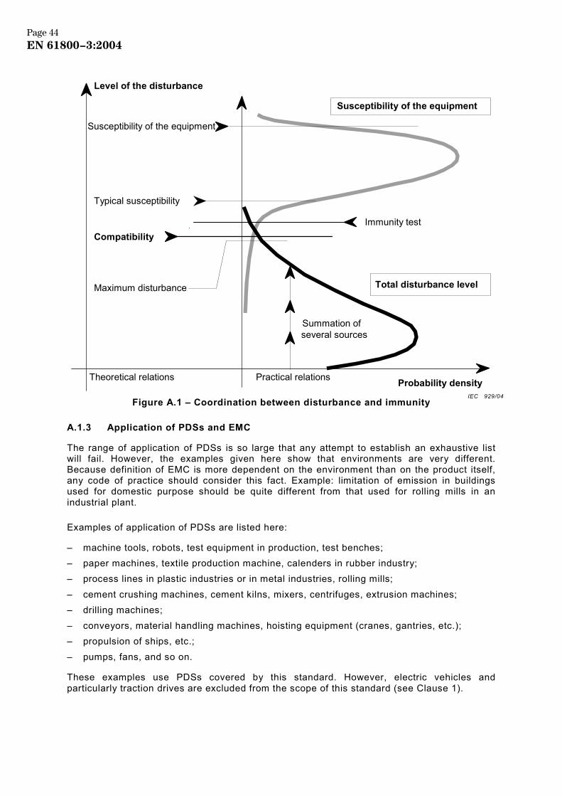
Theoretical relations Practical relations
Maximum disturbance
Compatibility
Typical susceptibility
Summation ofseveral sources
Total disturbance level
Immunity test
Susceptibility of the equipment
Level of the disturbance
Susceptibility of the equipment
Probability density Figure A.1 – Coordination between disturbance and immunity
A.1.3 Application of PDSs and EMC
The range of application of PDSs is so large that any attempt to establish an exhaustive list will fail. However, the examples given here show that environments are very different. Because definition of EMC is more dependent on the environment than on the product itself, any code of practice should consider this fact. Example: limitation of emission in buildings used for domestic purpose should be quite different from that used for rolling mills in an industrial plant.
Examples of application of PDSs are listed here:
– machine tools, robots, test equipment in production, test benches; – paper machines, textile production machine, calenders in rubber industry; – process lines in plastic industries or in metal industries, rolling mills; – cement crushing machines, cement kilns, mixers, centrifuges, extrusion machines; – drilling machines; – conveyors, material handling machines, hoisting equipment (cranes, gantries, etc.); – propulsion of ships, etc.; – pumps, fans, and so on.
These examples use PDSs covered by this standard. However, electric vehicles and particularly traction drives are excluded from the scope of this standard (see Clause 1).
IEC 929/04
Page 44EN 61800−3:2004
A.2 Load conditions regarding high-frequency phenomena
A.2.1 Load conditions during emission tests
The load on the motor normally has little effect on the EMC characteristics of the PDS. Therefore, the PDS need not be tested for EMC characteristics at all load conditions, but only at a load that is representative of all operating emissions. The manufacturer should certify that the load conditions he has selected for the test meet this criterion.
The radiated and conducted emissions of a PDS are mainly caused by sharp transitions of its output voltage that are used to produce low-frequency, or d.c. output power. The voltage spectrum of the waveform can have sufficient energy at high frequencies for the PDS to radiate electrical energy from its input power wires, cabinet, motor leads, and motor case. Since the radiated energy is caused by the voltage transitions, tests should be performed at conditions where the voltage transitions have the largest amount of high-frequency content. Tests need not be performed at other conditions.
The sharpness of output transitions can be affected by the switching speed of the power device that is used in the PDS. IGBTs (transistors) are extremely fast devices that in combination with the recovery characteristics of the diodes used in some types of inverters can cause dv/dt that can be greater than 1 000 V/µs. It is important to note that the abruptness of the diode recovery is an important component of this high dv/dt. Even though the level of the recovery current is load dependent, the abruptness of the diode recovery is not as dependent on the load level. Note that attenuation measures should be rated to cover saturation effects of filter elements (for example saturation of interference suppression inductors).
On the other hand, it is important to consider the effect of passive capacitive, resistive, or inductive power circuit components, such as snubber components that are used to control the rate of rise of this voltage. The output waveform with these devices present can have dv/dt characteristics that are load dependent. In this case, it is important that the PDS be tested at the worst case dv/dt point of operation.
A.2.2 Load conditions during immunity tests
The load on the motor normally has little effect on the EMC characteristics of the PDS. Therefore, the PDS need not be tested for EMC characteristics at all load conditions, but only at a load that is representative of all susceptibilities. The manufacturer should certify that the load conditions he has selected for the test meet this criterion.
Generally, load conditions do not affect the immunity of a PDS to low or high-frequency disturbances. The failures of the power and control circuitry are generally associated with voltage not current levels. Testing at light load does not detect slight changes in the settings of protective circuitry, i.e. over current, over voltage. If these levels are critical to the proper operation of a PDS, the test should verify the immunity at these points of operation.
If the torque-generating behaviour criterion is used, the load should be at such a level that it is possible to measure the torque disturbance associated with the low or high-frequency tests. This will require a motor and a torque-measuring device. The motor should have a load that can be used in the electromagnetic environment of the test. If indirect torque-measuring methods are used, the PDS should be operated at a load level which is sufficient for any torque disturbances to be measured.
Page 45EN 61800−3:2004
A.2.3 Load test
A light load test, i.e. a test with the motor running at no load, can be used to verify the EMC characteristics of a PDS if the above conditions are met. Tests can even be performed using passive power resistors and inductors that simulate the load condition of a motor. It is also important to note that the motor case can act as an antenna element. If a passive load is used, this antenna effect should also be simulated.
The manufacturer of the PDS should provide certification that the load on the PDS during any test will produce the worst case or most sensitive conditions for his particular product. This certification can be by test of a representative product, or by calculation or simulation.
A.3 Some immunity aspects
A.3.1 Power frequency magnetic fields
Testing according to IEC 61000-4-8 is usual where components sensitive to magnetic field are used. PDSs frequently use Hall effect current sensors. However, these sensors are designed to operate in locations where high levels of magnetic fields exist (close vicinity of power conductors). Those amplitudes are much higher than the levels of the test according to IEC 61000-4-8. For example, it can be calculated that a 10 A current (assumed to be alone on an infinite straight line) produces a magnetic field of 320 A/m at 5 mm. It can therefore be considered that the disturbance applied by the test is negligible compared to the operating environment of this sensitive component.
A.3.2 Electromagnetic field immunity test
A.3.2.1 Low level electromagnetic fields (EM-fields)
Industrial, scientific and medical (ISM) radio-frequency equipment, some welders, dryers, etc. can be sources of low-level electromagnetic fields. These devices are all present in the domestic and industrial environment. The resulting field strengths are expected to be less than 3 V/m at the enclosure port of the PDS.
The established experience with PDSs shows that provided an intrinsic operational availability is realised, the radiated EM-fields from other PDSs and other low level EM-fields from commercial broadcasting stations are not matters of complaint.
A.3.2.2 Complementary test
The field strength decreases in inverse proportion to the distance between the transmitting antenna and the possible victim, and increases only with the square root of antenna input power. Therefore, attention should be drawn to the transmitters which can be operated in close proximity about 1 m from the PDS. These communication devices are the dominant radiating interference sources affecting electronic equipment. Examples of usual local sources of continuous high-frequency disturbances are mobile telecommunication equipment such as walkie-talkies or cordless telephones.
A large PDS cannot be installed and operated correctly in a test site (shielded room) for the test of IEC 61000-4-3. Therefore, to verify the complete assembly of the PDS in the case where only sub-components have been tested, an alternative complementary test can be performed with radio-communication devices of common industrial use as emitters.
Page 46EN 61800−3:2004
During the test, the PDS is operated and monitored according to 5.1.3, and under normal operating conditions (for example doors closed).
Because this test is not performed in a shielded room, only transmitters which are legally approved for use at the test location can be used. The following transmitters are recommended:
– devices such as walkie-talkies which are commonly used in close proximity at the user’s premises;
– digital mobile telephone, unless they are prohibited at the operating location at the user’s premises, and if they are able to transmit at their rated power.
Care should be taken that the battery pack or the power supply of the transmitter is at full capability. If the transmitter is able to adjust the power of the emission (as battery saving feature), care should be taken that this possibility is disabled. The list and characteristics of transmitter (type, power and frequencies) used during the test should be stated by the manufacturer in the user information.
The transmitter is hand-held close to a vertical surface of the CDM/BDM. The closest point of the antenna to the PDS is between 0,5 m and 1,0 m from the PDS. The transmitter is switched from "receive" to "transmit" and back to "receive". Care should be taken that the dwell time of the transmission is not less than the time necessary for the PDS to be able to respond. In the case of a telephone type of device, where the user cannot switch between "transmit" and "receive", a telephone number is transmitted instead.
There should be at least three transmissions for each antenna orientation: vertical, horizontal in a plane parallel to the surface of the PDS, and perpendicular to the PDS (pointing towards the PDS).
This procedure should be carried out:
– on at least five positions on each vertical surface of the CDM/BDM; – at all openings of these vertical surfaces, a ventilation grille is considered to be one
opening; – at the surface of the motor, if it includes sensors.
The whole procedure should then be repeated for at least two different transmission frequencies.
A.4 High-frequency emission measurement techniques
A.4.1 Impedance/artificial mains network (AMN)
A.4.1.1 Circuit of AMN
Since the high-frequency disturbance source within a drive has a source impedance, the disturbance voltage measurement is affected by the network impedance. Particularly at lower frequencies, the impedance of the mains can be regarded as inductive. However, there can be resonances due to various capacitances of the system. For further information, see 6.6 of IEC 61000-2-3 (1992).
Where possible, an AMN should be used to standardise the supply impedance used during type tests. This improves the repeatability between different test sites.
Page 47EN 61800−3:2004
The characteristics of various networks are defined in 5.1 of CISPR 16-1 (2002). For the frequency range of disturbance voltage measurements defined in this standard, the 50 Ω // 50 µH network or the 50 Ω // 50 µH + 5 Ω network can be used. Between 150 kHz and 30 MHz, the equipment under test (power drive system) sees an impedance to earth of 50 Ω in parallel with 50 µH, regardless of the impedance of the incoming mains supply.
The AMN contains the circuit reproduced for each phase. The neutral, if used, is connected through a circuit identical to that used for each phase.
A.4.1.2 PDS with which the AMN cannot be used
A.4.1.2.1 Reasons of impossibility
At lower frequencies, the inductors inside the 50 Ω // 50 µH AMN add 50 µH to the impedance of the mains supply. The inductors inside the 50 Ω // 50 µH + 5 Ω AMN add 300 µH. This additional impedance can prevent correct operation of some PDSs (for example commutation notches become excessively wide at high current and low firing angle, if the supply inductance is too high). In these cases, the AMN cannot be used.
The AMNs described above are only rated for use up to 100 A, so they cannot be used for PDSs rated greater than this. For a very large PDS (example rated current above 400 A), the supply impedance will be lower than the impedance of the AMN. In this case, use of an AMN would give excessively high readings.
For supply voltages higher than 400 V nominal, it can be difficult to obtain an AMN on the market.
For these cases, the PDS should be connected directly to the mains supply and the disturbance voltage can be measured with a high impedance probe.
A.4.1.2.2 High impedance probe
When an AMN is not used, the disturbance voltage can be measured using a high impedance probe, as described in 5.2.2 of CISPR 16-1 (2002). Since the power frequency current does not pass through the probe, it can be used with PDSs of even the highest current ratings.
By adjusting the value and voltage rating of the capacitor, this probe can be used with supplies at least up to 1000 V. If the capacitor value is reduced, its effect on the scaling of the measurement should be allowed for in calibration, as stated in CISPR 16-1.
The probe is connected between the line and the reference earth. If the CDM/BDM has an earthed metal frame, this can be taken as the reference earth. This connection should be to the supply leads as they enter the CDM/BDM. The connections to the probe should be as short as possible, preferably less than 0,5 m.
CISPR 16-1 provides a warning about the need to minimise the loop area formed between the lead connected to the probe, the conductor tested and the reference earth. This is to reduce susceptibility to magnetic fields.
Page 48EN 61800−3:2004
A.4.1.2.3 Alternative method for high current PDS
In some cases it can be difficult to use the high impedance probe because of safety reasons during changing of phases, and the readings can be several tens of decibels higher (because of mismatched impedance) than those which are obtained with an AMN measurement.
An alternative method, which has been experienced in some countries for a number of years, uses a low current AMN (for example 25 A) as a voltage probe, even with a high current PDS (above several hundreds of amperes). This method is described in Clause A.5 of CISPR 16-2 (2003). The PDS is not disconnected from its supply network.
The load side of the AMN should be connected to the supply lines of the PDS at the power port terminals by a 1 m cable. There should be some inductance (for example connection cabling) between the PC and the AMN connection. The mains side of the AMN should be left open (for example no connection to peripherals). The receiver should be connected to the AMN as usual. The measurement results, with this method, are quite similar to that of a virtual AMN of several hundreds of amperes.
A.4.2 Performing high-frequency emission tests
A.4.2.1 Measuring apparatus
A.4.2.1.1 Purpose of the information
For definitive information, reference should be made to the normative parts of this standard and of CISPR 11 and CISPR 16-1. Some additional clarifications are given here for those users of this standard who are not familiar with radio-frequency disturbance measurement methods.
A.4.2.1.2 Spectrum analysers
Spectrum analysers are frequently used for evaluation of high-frequency disturbances. However, many spectrum analysers are not fully compliant with CISPR 16-1 and problems can occur.
If there is a lack of front-end selectivity, intermodulation can occur, leading to incorrect readings. Some spectrum analysers do not have the correct bandwidths, again resulting in error.
Spectrum analysers use peak detectors for normal scanning. However, CISPR standards require the use of receivers with special detectors known as quasi peak and average. Sometimes, the quasi-peak detector is known as a "CISPR detector". Some spectrum analysers have these available as an option. CISPR 16-1 requires high overload capabilities for quasi-peak and average detectors, which can be a problem for many spectrum analysers.
If a spectrum analyser is fully compliant with CISPR 16-1, this should be stated by the manufacturer of the analyser.
A.4.2.1.3 Suitability of test receivers
To determine whether an instrument (spectrum analyser or test receiver) is suitable, the supplier of the instrument should be asked whether the instrument is fully compliant with CISPR 16-1. But to aid understanding of the requirements, a summary of some of the main features is given here.
Page 49EN 61800−3:2004
For mains terminal disturbance measurements, a receiver should cover the frequency range 150 kHz to 30 MHz. Both quasi-peak and average detectors should be present. The bandwidth should be 9 kHz.
The frequency range 9 kHz to 150 kHz is also available on some receivers. In this frequency range, a quasi-peak detector should be available and the bandwidth should be 200 Hz.
The receiver for electromagnetic radiation disturbance (radiated emissions) measurements should cover the band 30 MHz to 1 000 MHz. Here, the bandwidth is 120 kHz and a quasi-peak detector should be used.
A.4.2.2 Measuring techniques
A.4.2.2.1 Aliasing
The receiver should be allowed to remain tuned to a given frequency for a period of time which is long enough to allow the detector output to settle. If a test receiver (or spectrum analyser) is scanned too quickly, the detector will not settle properly and a phenomenon called aliasing will occur, resulting in incorrect readings. This point is particularly significant with power electronics, including PDSs, due to low pulse repetition frequencies (50/60 Hz to several kilohertz). If peaks or troughs in the waveform appear to move across the screen, there is aliasing and the sweep time should be increased.
In the type of spectrum analyser frequently used for evaluation of high-frequency disturbances, a local oscillator is swept across the frequency range. This should not be confused with analysers which use Fast Fourier Transform of time domain samples.
At those frequencies where the readings are close to the limit, a measurement should be made without the receiver scanning. This avoids the problem of inaccuracy caused by aliasing at these frequencies.
A.4.2.2.2 Peak, quasi-peak and average
Peak, quasi-peak and average detectors will give the same reading in the presence of continuous sine-wave signal, provided that the bandwidth is the same. In the presence of an impulsive signal, such as PWM, the highest reading will be given by the peak detector and the lowest by the average detector. The difference between the readings produced by the different detectors is greatest when the pulse repetition frequency is much lower than the receiver bandwidth.
A.4.2.2.3 Ambient noise
The requirements for limitation of ambient noise are given in 6.1 of CISPR 11 (2003).
Care should be taken to ensure that the ambient noise does not cause erroneous readings. When monitoring the ambient noise level from the incoming mains supply, it should be noted that an open-circuit contactor or switch will provide attenuation that will not be present when the PDS is running.
A.4.2.2.4 Disposition of PDS during the test
The test is intended to simulate actual operating conditions. Therefore, the equipment should be operated in a manner which can be expected in normal use. For example, covers and doors which are closed during normal operation should be closed during the test. Some other requirements are given in the normative part of this standard.
Page 50EN 61800−3:2004
A.4.2.2.5 Measuring radiated emissions
Antennas and test sites for radiated emissions are described in detail in 5.5 and 5.6 of CISPR 16-1 (2002).
To standardise the measurements of radiated emissions, a special open-area test site (OATS) is used. This contains a metallic ground plane with sufficient conductivity to give consistent reflectivity.
The equipment under test is mounted on a turntable to enable the radiated emissions in the various directions to be measured.
To ensure that measurements are in the far field at the lowest frequency (30 MHz), the antenna is mounted 10 m or 30 m from the equipment under test.
The antenna is raised and lowered in both vertical and horizontal polarizations to find the maximum emission at any given frequency.
A.4.2.2.6 In situ tests
When equipment cannot be tested on a test site, tests are performed in situ. In this case, extra care should be taken to avoid problems caused by ambient noise, as described above.
Testing in situ is not as repeatable as testing on a test site. Therefore, some care should be taken when using the results of in-situ testing on one site to predict compliance for a product produced in quantity.
One approach, used in the United States when tests have not been carried out on a test site, is to perform the in-situ test in the first three locations where the equipment is installed. If the equipment is found to comply with the limits in all three locations, it is considered that the equipment will comply with the limits in the general case.
A.4.3 Established experience with high power PDSs
For several decades, the experience in different countries has shown that the established procedures of legislation and protection of radio-communication services against high-frequency disturbances have been proved in practice with excellent results. As an example, the procedure which has been used in Germany for many years is described below.
Under this procedure, because high power equipment intended for use in the second environment is part of an installation, it is not tested on a test-site. See [4]1. The same rules apply to equipment which is built by the user himself, under his own responsibility; see [5]. The emission limits of such a high power installation are referenced to the actual boundary of the installation terrain, even in the case of measurement and control equipment which is intended to be installed there. The emission limits have been applied with respect to the boundary of the installation (the measurement point for conducted disturbance voltages is the low-voltage secondary of the next available medium-voltage transformer, and for the radiated emissions a 30 m distance to the boundary); see [4] and [5].
As a result, the procedure stated in 6.5 follows this experience. Such a use of a PDS (category C4) requires EMC competence. Such competence should be applied to the design of the apparatus, or the manufacturer and the user should define the best economical compatibility levels in a specific environment.
——————— 1 The figures in square brackets refer to the bibliography.
Page 51EN 61800−3:2004
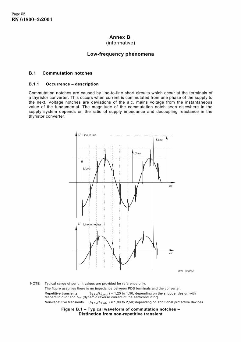
Annex B (informative)
Low-frequency phenomena
B.1 Commutation notches
B.1.1 Occurrence – description
Commutation notches are caused by line-to-line short circuits which occur at the terminals of a thyristor converter. This occurs when current is commutated from one phase of the supply to the next. Voltage notches are deviations of the a.c. mains voltage from the instantaneous value of the fundamental. The magnitude of the commutation notch seen elsewhere in the supply system depends on the ratio of supply impedance and decoupling reactance in the thyristor converter.
U
U
ωt
U LWM
ULRM
ULSM
Line to line
Line to neutral
ωt
NOTE Typical range of per unit values are provided for reference only. The figure assumes there is no impedance between PDS terminals and the converter. Repetitive transients (ULRM/ULWM ) = 1,25 to 1,50; depending on the snubber design with respect to di/dt and IRR (dynamic reverse current of the semiconductor). Non-repetitive transients (ULSM/ULWM ) = 1,80 to 2,50; depending on additional protective devices.
Figure B.1 – Typical waveform of commutation notches – Distinction from non-repetitive transient
IEC 930/04
Page 52EN 61800−3:2004
Analysis of notches considers a wider range of frequencies than normal harmonic analysis. Their time-domain characteristics cause effects which cannot be understood by a simple harmonic analysis. Therefore, they are analysed in the time domain using an oscilloscope.
The following should first be remembered:
– in simple cases where the rule applies, it is assumed that the network impedance can be modelled with a pure reactance: Z = Lω; (this assumption is not valid in cases where capacitors or long cables are present, resonances can occur in such cases);
– the immunity against commutation notches is classified in 2.5.4.1 of IEC 60146-1-1 (1991) where their measurement is defined in depth (in % of ULWM) and in area (depth multiplied by width, in %degrees); IEC 60146-1-1 defines ULWM as the maximum instantaneous value of UL excluding transients (therefore this is the amplitude), where UL is the line-to-line voltage on the line side of the converter or transformer, if any.
If the converter does not include any inductance, the depth d, of the principal notch in the line-to-line voltage at the terminals of the converter itself (not the terminals of the BDM/CDM) is given by
d = 100 sin α (%)
where α represents the firing angle of a phase controlled converter (referred to the natural commutation point of a diode);
– the principal notch is characterised by a value of 0 V (line-to-line voltage at the converter's terminals);
– the approximation gives an under-evaluation of d for α < 90 °, and an over-evaluation of d for α > 90 °.
The notch area a, can be approximated by a simple relationship (example of a three-phase bridge, see the conditions of the approximation in the note below):
a = 8 000 (Zt × I1L/UL) (% degrees)
where Zt is the total line impedance per phase (here assumed to be a pure reactance), including
any impedance in the CDM; I1L is the fundamental component of the line-side current, and UL is the line-to-line voltage.
It can be seen that the worst case occurs when the PDS is at current limit conditions.
NOTE During commutation angle u, from α to (α + u), the commutating voltage is:
2 UL sin ωt
and 2 UL sin ωt = 2 Lt dI/dt
Page 53EN 61800−3:2004
the area of the commutation notch is
( ) ∫∫+ α+u
tu
dθdθdt
dtdi
L=dUA=α
α
αθθ 2 (in volt x radian)
A = 2 Lt ω Iα which means A = 2 Zt Iα
where Iα is the commutated current.
To take into account the ripple in a three-phase bridge, assume Iα ≈ 0,75 Id , where Id is the d.c. current:
A = 1,5 Zt Id
and with a in %degrees
a = 100 A (360/2 π) (1/ 2 UL) = 6 077 (Zt Id/UL)
a = 7 794 (Zt I1L/UL)
a ≈ 8 000 (Zt I1L/UL) or in per units values a ≈ 4 500 (zt iL)
B.1.2 Calculation
B.1.2.1 General assessment
When the assumptions listed above are valid, the notch depth at the PC is:
dPC % = 100 sin α ( Zc/(Zc + Zd) ) = 100 sin α (Zc/Zt)
where Zt is the total line impedance.
Zt = Zc + Zd
where Zd is the decoupling reactance between the PC and the converter terminals (whether included
or not in the CDM); Zc is the supply network impedance at the PC.
The amplitude of the ability of control of the converter (for example the case of a three-phase controlled bridge), is often represented by sin α. The notch depth varies from 100 % at the converter terminals to 0 % at a zero impedance source.
Adding a decoupling reactance Zd between the PC and the BDM reduces the notch depth and increases the notch width at the PC, but the notch area remains constant.
aPC = 8 000 (Zc × I1L/UL) (% degrees)
In simple cases where the above assumptions apply, these equations can be used to define the required decoupling reactance. Knowing the notch depth limit (see Table B.1) and the control amplitude ability of the converter, the notch depth at the PC gives the ratio:
Zc/(Zc + Zd)
Then Zc, defined by the user, allows calculation of Zd by the installer, from which the internal decoupling reactance if any (given by the manufacturer) can be subtracted. The remaining value is the reactance to be added for correct decoupling.
NOTE The calculations above do not take account of transients at the beginning and at the end of the notch.
Page 54EN 61800−3:2004
B.1.2.2 Practical rules
The calculation above defines the practical rule for decoupling the emission by means of a reactance Zd. This is summarised below. The fundamental relations, assuming the network impedance is a pure reactance, are:
Zc = Lc × ω
Zt = Zc + Zd
dPC % = 100 sin α (Zc/Zt)
aPC %degrees = 8 000 (Zc × I1L/UL)
In the case of multiple converters, connected to the same line, 3.5 of IEC 60146-1-2 should be considered.
However, it should be remembered that compliance with the notch emission criterion does not automatically ensure compliance with harmonic emission criteria. Similarly, compliance with harmonic emission criteria does not automatically ensure compliance with the notch emission criteria. The immunity aspect is not entirely covered by the harmonic distortion criteria. Indeed, since the harmonic criterion does not imply any phase relationship between the different harmonic components, it does not prevent a particular voltage waveform from being applied to the PDS. Because the particular waveform of commutation notches (dv/dt, possible zero crossing) affects operation of snubbers or can affect electronic control operation as well, a particular immunity criterion is stated in IEC 61800-1 (1997) and in IEC 61800-2 (1998), it is even defined as electrical service conditions in 4.1.1 of these standards.
B.1.3 Recommendations regarding commutation notches
B.1.3.1 Emission
The recommendation does not apply to power converters with such a structure that commutation notches are known not to exist or to have only negligible amplitude.
NOTE 1 For example, an indirect converter of the voltage source inverter type with an active front end equipped with a decoupling filter designed for attenuation of the effects of the switching frequency does not produce notches. A simple diode rectifier produces notches of negligible amplitude. The main practical case where emission of notches should be considered is the case of thyristor converters (line commutated).
Compliance with the recommendations related to commutation notches does not avoid the need to verify compliance with the requirements for harmonics. The depth of the principal notch at the PC (PCC or IPC) should be limited according to Table B.1, with a line impedance assumed to be a pure reactance:
Z = L ω
and having a value of 1,5 % (related to the rated power of the PDS).
NOTE 2 When installing the PDS, the line impedance is practically defined from the short-circuit power Ssc at the PC:
Zsc = ULN2/Ssc
Page 55EN 61800−3:2004
Table B.1 – Maximum allowable depth of commutation notches at the PC
First environment Second environment
Maximum notch depth
20 %
Class C of IEC 60146-1-1 or comply with the requirements of the local supply authority
40 %
Class B of IEC 60146-1-1 or agreement with the user
NOTE 3 This rule cannot be used in cases where resonances can be expected due to capacitors or long length of cables.
NOTE 4 In the case of certain distribution networks, special consideration may be required (for example internal distribution networks in hospitals). In such cases, the conditions should be specified by the user.
Compliance may be determined by calculation, simulation or measurement.
If the PDS deviates from this recommendation, and in order to make the user able to comply with this recommendation, the manufacturer should provide the following information in the user documentation:
– the maximum and the minimum line impedance for correct operation of the CDM/BDM; – details of the decoupling reactance Zd if any, that is included in the CDM/BDM. – details of the available decoupling reactances Zd which can be delivered as optional items. NOTE 5 The maximum line impedance is directly related to the maximum notch area at the PC (see B.1.1).
However, in the case of multiple PDSs connected to the same PC, notch limitation is a system consideration and a simple rule cannot be defined.
NOTE 6 The main practical case where immunity against notches should be considered for other equipment is the case of RFI filters.
B.1.3.2 Immunity
The harmful effect of notches on a PDS can be much greater than that which would be indicated by a frequency domain analysis of their contribution to the total harmonic distortion. Therefore, a time domain analysis of commutation notches is necessary. Note that the stress due to harmonics and commutation notches affects the electronic control and some power devices as well (snubbers for instance). Because electronic control malfunctions will occur immediately, and snubbers have a short thermal time constant, the duration of a test, if any, for permanent conditions need not exceed 1 h.
Some practical cases where immunity against notches should be considered are:
– where operation is affected instantaneously, for example the effect on electronic synchronisation circuits where the zero crossing of voltage is taken as reference;
– thermal overload, for example overload of snubber circuits in the power converter; – overvoltage on L-C circuits, for example RFI filters.
Page 56EN 61800−3:2004
B.2 Definitions related to harmonics and interharmonics
B.2.1 General discussion
B.2.1.1 Resolution of non-sinusoidal voltages and currents
Classical Fourier series analysis (IEV 101-13-08) enables any non-sinusoidal but periodic quantity to be resolved into truly sinusoidal components at a series of frequencies, and in addition, a d.c. component. The lowest frequency of the series is called the fundamental frequency (IEV 101-14-49). The other frequencies in the series are integer multiples of the fundamental frequency, and are called harmonic frequencies. The corresponding components are referred to as the fundamental and harmonic components, respectively.
The Fourier transform (IEV 101-13-09) may be applied to any function, periodic or non-periodic. The result of the transform is a spectrum in the frequency domain, which in the case of a non-periodic time function is continuous and has no fundamental component. The particular case of application to a periodic function shows a line spectrum in the frequency domain, where the lines of the spectrum are the fundamental and harmonics of the corresponding Fourier series.
NOTE 1 When analysing the voltage of a power supply system, the component at the fundamental frequency is the component of the highest amplitude. This is not necessarily the first line in the spectrum obtained when applying a DFT to the time function.
NOTE 2 When analysing a current, the component at the fundamental frequency is not necessarily the component of the highest amplitude.
B.2.1.2 Time varying phenomena
The voltages and currents of a typical electricity supply system are affected by incessant switching and variation of both linear and non-linear loads. However, for analysis purposes they are considered as stationary within the measurement window (approximately 200 ms), which is an integer multiple of the period of the power supply voltage. Harmonic analysers are designed to give the best compromise that technology can provide (see IEC 61000-4-7 (2002)).
B.2.2 Phenomena related definitions
B.2.2.1 fundamental frequency a frequency, in the spectrum obtained from a Fourier transform of a time function, to which all the frequencies of the spectrum are referred. For the purposes of IEC 61800, it is the same as the power frequency supplying the converter, or supplied by the converter according to the case which is considered
[IEV 101-14-50, modified]
NOTE 1 IEV 551-20-01 and IEV 551-20-02 defines the components as result of the Fourier analysis, frequencies are therefore a consequence. In this clause, the definitions follow the approach of SC77A defining first the frequencies, components being a consequence. There is no contradiction between the two different approaches.
NOTE 2 In the case of a periodic function, the fundamental frequency is generally equal to the frequency of the function itself (see IEV 551-20-03 and IEV 551-20-01). The above definition corresponds to the genuine definition of "reference fundamental frequency" according to IEV 551-20-04 and IEV 551-20-02, for which the term "reference" may be omitted where there is no risk of ambiguity.
NOTE 3 In case of any remaining risk of ambiguity, the power supply frequency should be referred to the polarity and speed of rotation of the synchronous generator(s) feeding the system.
NOTE 4 This definition may be applied to any industrial power supply network, without regard to the load it supplies (a single load or a combination of loads, rotating machines or other load), and even if the generator feeding the network is a static converter.
Page 57EN 61800−3:2004
B.2.2.2 fundamental component (or fundamental) the component whose frequency is the fundamental frequency
B.2.2.3 harmonic frequency a frequency which is an integer multiple of the fundamental frequency. The ratio of this frequency to the fundamental frequency is named harmonic order (recommended notation " h "), see IEV 551-20-07, IEV 551-20-05 and IEV 551-20-09
B.2.2.4 harmonic component any of the components having a harmonic frequency. Its value is normally expressed as an r.m.s. value
NOTE For brevity, such a component may be referred to simply as a harmonic.
B.2.2.5 interharmonic frequency any frequency which is not an integer multiple of the fundamental frequency.
See IEV 551-20-07, IEV 551-20-05 and IEV 551-20-09
NOTE 1 By extension of the harmonic order, the interharmonic order is the ratio of interharmonic frequency to the fundamental frequency. This ratio is not an integer (recommended notation " m ").
NOTE 2 In the case where " m < 1" the term of sub-harmonic frequency may also be used (see IEV 551-20-10).
B.2.2.6 interharmonic component a component having an interharmonic frequency. Its value is normally expressed as an r.m.s. value
NOTE 1 For brevity, such a component may be referred to simply as an interharmonic.
NOTE 2 For the purposes of IEC 61800, and as stated in IEC 61000-4-7, the time window has a width of 10 fundamental periods (50 Hz systems) or 12 fundamental periods (60 Hz systems), i.e. approximately 200 ms. The difference in frequency between two consecutive interharmonic components is, therefore, approximately 5 Hz. In case of other fundamental frequencies, the time window should be selected between 6 fundamental periods (approximately 1000 ms at 6 Hz) and18 fundamental periods (approximately 100 ms at 180 Hz).
B.2.2.7 harmonic content sum of the harmonic components of a periodic quantity
[IEV 551-20-12]
NOTE 1 The harmonic content is a time function. NOTE 2 For practical analysis, an approximation of the periodicity may be necessary. NOTE 3 The harmonic content depends on the choice of the fundamental component. If it is not clear from the context which one is used, an indication should be given. NOTE 4 The r.m.s. value of the harmonic content is
( )∑=
=
=Hh
hhQHC
2
2
where Q represents either current or voltage; h is the harmonic order (according to B.2.2.3); H is 40 for the purposes of this standard.
Page 58EN 61800−3:2004
B.2.2.8 total harmonic distortion (THD) ratio of the r.m.s. value of the harmonic content to the r.m.s. value of the fundamental component or the reference fundamental component of an alternating quantity
[IEV 551-20-13]
NOTE 1 The harmonic content depends on the choice of the fundamental component. If it is not clear from the context which one is used, an indication should be given. NOTE 2 The total harmonic ratio may be restricted to a certain harmonic order (recommended notation " H "), 40 for the purpose of this standard.
∑=
=
=
Hh
h
hQQTHD
2
2
1
where in addition to notations in B.2.2.7 Q1 is the r.m.s. value of the fundamental component.
B.2.2.9 total distortion content quantity obtained by subtracting from an alternating quantity its fundamental component or its reference fundamental component
[IEV 551-20-11]
NOTE 1 The total distortion content includes harmonic components and interharmonic components if any. NOTE 2 The total distortion content depends on the choice of the fundamental component. If it is not clear from the context which one is subtracted, an indication should be given. NOTE 3 The total distortion content is a time function. NOTE 4 An alternating quantity (abbreviated as Q) is a periodic quantity with zero d.c. component.
NOTE 5 The r.m.s. value of the total distortion content is 21
2 QQDC −=
where notations come from B.2.2.7 and B.2.2.8. See also IEV 101-14-54 and IEV 551-20-06.
B.2.2.10 total distortion ratio (TDR) ratio of the r.m.s value of the total distortion content to the r.m.s. value of the fundamental component or the reference fundamental component of an alternating quantity
[IEV 551-20-14]
NOTE The total distortion ratio depends on the choice of the fundamental component. If it is not clear from the context which one is used an indication should be given.
Q
QDCTDR
1
21
2
1
−==
B.2.2.11 total distortion factor (TDF) ratio of the r.m.s. value of the total distortion content to the r.m.s. value of an alternating quantity
[IEV 101-14-55 and IEV 551-20-16]
Page 59EN 61800−3:2004
NOTE 1 The total distortion factor depends on the choice of the fundamental component. If it is not clear from the context which one is used an indication should be given.
Q
QDCTDF
21
2 −==
NOTE 2 The ratio between TDF and TDR equals the ratio between the r.m.s. value of the fundamental component and the total r.m.s. value. It is the fundamental factor (IEV 161-02-22):
11 ≤==QQ
TDRTDFFF
B.2.2.12 individual distortion ratio (IDR) the ratio of any component to the fundamental.
1
QQIDR h=
B.2.3 Conditions of application
B.2.3.1 Reference values
For the purposes of this standard and for clarity, limits are referred to the corresponding rated value.
Limits for THD and TDR are applied to:
∑=
=
=
Hh
h N
hQQTHD
2
2
1 and
Q
QQTDR
N1
21
2 −= or
1N
hQQ
IDR =
where QN1 is the rated r.m.s. value of the fundamental.
NOTE 1 It is important to note that THD does not include interharmonics, and that the upper limit H is generally 40. TDR does include interharmonics and frequencies above the order 40 up to 9 kHz. If interharmonics and emissions at frequencies above order 40, are negligible, THD and TDR are equal. The total distortion factor TDF, referring the distortion to the total r.m.s. value of the voltage or of the current is rarely used and should be disregarded to avoid confusion.
Assessment of emission should be made under the operating conditions which provide the maximum value of the harmonic content in current according to IEC 61000-3-12, and in reference to the rated value. Nevertheless, interharmonics should be considered separately.
NOTE 2 The harmonic content in current (HCI) is designated as the total harmonic current (THC) in IEC 61000-3-12, where interharmonics can be disregarded, it represents a good approximation of the total distortion content in current (DCI)
( ) )( 240
2
2 21IIDCI IHCITHC
h
hh −=≈== ∑
=
=
B.2.3.2 Systems and installations
A PDS is generally a component of a larger system which can be as large as a complete processing line in the paper or metal industry. To avoid any confusion in this standard, the word "installation" is used exclusively to designate the complete installation which is connected to a PCC (point of common coupling) on a public power supply network.
Page 60EN 61800−3:2004
B.2.3.3 Load conditions
For the system, the steady state conditions represent the worst case conditions provided that the overload conditions (acceleration or other) do not exceed a total duration of 5 % in a 24 h period, and 1 % in a 7 day period. If the load of the system is defined by a cycle, assessment of harmonic emission during a period of highest load should be performed according to the measurement method defined in IEC 61000-4-7.
Overload conditions are not considered for assessment of low voltage PDS with rated input current below 75 A, see B.3.2.2.
B.2.3.4 Agreed power
The agreed power SST defines the equivalent reference current ITN (total r.m.s. value):
SST = UN x ITN x 3
where UN is the nominal (or declared) line-to-line voltage at the PCC and ITN is the reference current.
Note that ITN is close to the tripping current value of the main circuit breaker of the installation. SST represents the power which can be delivered at any time, by the public supply network, to the installation. It can be assumed that for each agreed internal power there exists a reasonable short-circuit power (fault level) SSC defined at the PCC. This is the responsibility of the power distribution authority.
NOTE The "agreed power" results from an agreement between the user (owner of the installation) and the utility authority.
Where the agreed power is used to define the reference current to which harmonic currents are compared in order to express them in p.u. (per unit), the reference current ITN1 is by convention equal to ITN .
B.2.3.5 Agreed internal power (extension of the definition of agreed power)
The agreed internal power SITA , for an installation at a defined IPC "α", defines the equivalent reference current ITNA (total r.m.s. value) for the part A of the installation fed from α:
SITA = UN x ITNA x 3
where UN is the rated line-to-line voltage at the IPC "α".
Note that ITNA is the rated current of the feeding section of the part A of the installation. ITNA is close to the rating of the circuit-breaker protecting this part A. It can be assumed that for each agreed internal power there exists a reasonable short-circuit power (fault level) SSCα defined at the IPC "α". This is the responsibility of those in charge of internal power distribution.
B.2.3.6 Short-circuit current ratio of the source in the installation
RSI is the ratio of the short-circuit power of the source at a defined PC to the rated apparent power of the installation, or of a part of the installation, supplied from this PC (see Figure B.2):
RSIA = SSCα/SITA = ISCα/ITNA
Page 61EN 61800−3:2004
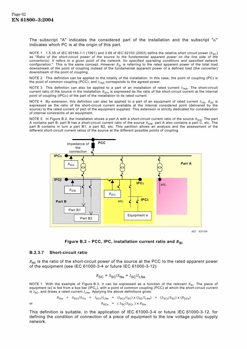
The subscript "A" indicates the considered part of the installation and the subscript "α" indicates which PC is at the origin of this part.
NOTE 1 1.5.35 of IEC 60146-1-1 (1991) and 3.69 of IEC 62103 (2003) define the relative short circuit power (RSC) as "Ratio of the short-circuit power of the source to the fundamental apparent power on the line side of the convertor(s). It refers to a given point of the network, for specified operating conditions and specified network configuration.". This is the same concept. However RSI is referring to the rated apparent power of the total load downstream of the point of coupling instead of the fundamental apparent power of a defined load (the converter) downstream of the point of coupling.
NOTE 2 This definition can be applied to the totality of the installation. In this case, the point of coupling (PC) is the point of common coupling (PCC), and ITNA corresponds to the agreed power.
NOTE 3 This definition can also be applied to a part of an installation of rated current ITNA. The short-circuit current ratio of the source in the installation RSIA is expressed as the ratio of the short-circuit current at the internal point of coupling (IPCα) of the part of the installation to its rated current.
NOTE 4 By extension, this definition can also be applied to a part of an equipment of rated current ITNi. RSIi is expressed as the ratio of the short-circuit current available at the internal considered point (delivered by the source) to the rated current of part of the equipment supplied. This extension is strictly dedicated for consideration of internal constraints of an equipment.
NOTE 5 In Figure B.2, the installation shows a part A with a short-circuit current ratio of the source RSIA. The part A contains part B, part B has a short-circuit current ratio of the source RSIB, part A also contains a part C, etc. The part B contains in turn a part B1, a part B2, etc. This partition allows an analysis and the assessment of the different short-circuit current ratios of the source at the different possible points of coupling.
Figure B.2 – PCC, IPC, installation current ratio and RSI
B.2.3.7 Short-circuit ratio
RSC is the ratio of the short-circuit power of the source at the PCC to the rated apparent power of the equipment (see IEC 61000-3-4 or future IEC 61000-3-12):
RSC = SSC/SNe = ISC/ILNe
NOTE 1 With the example of Figure B.3, it can be expressed as a function of the relevant RSI. The piece of equipment (e) is fed from a bus bar (IPCδ), with a point of common coupling (PCC) at which the short-circuit current is ISC, and draws a rated current ILNe. Applying the above definitions gives:
RSIe = SSCδ/SITe = ISCδ/ILNe = (ISCδ/ISC) x (ISC/ILNe) = (SSCδ/SSC) x (RSCe)
or RSCe = ( SSC/SSCδ ) x RSIe
This definition is suitable, in the application of IEC 61000-3-4 or future IEC 61000-3-12, for defining the condition of connection of a piece of equipment to the low voltage public supply network.
IEC 931/04
Part B
Part B1
Part B2
PCC
IPCα
IPCβ etc.
etc.
Equipment e
IPCγ
IPCδ
Part A
Impedance of the
connection
RSIA
RSIBRSIC
Page 62EN 61800−3:2004
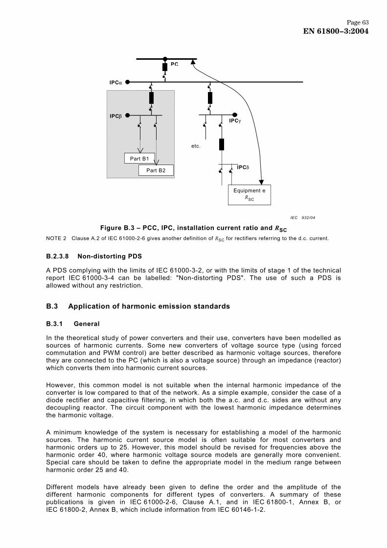
Figure B.3 – PCC, IPC, installation current ratio and RSC NOTE 2 Clause A.2 of IEC 61000-2-6 gives another definition of RSC for rectifiers referring to the d.c. current.
B.2.3.8 Non-distorting PDS
A PDS complying with the limits of IEC 61000-3-2, or with the limits of stage 1 of the technical report IEC 61000-3-4 can be labelled: "Non-distorting PDS". The use of such a PDS is allowed without any restriction.
B.3 Application of harmonic emission standards
B.3.1 General
In the theoretical study of power converters and their use, converters have been modelled as sources of harmonic currents. Some new converters of voltage source type (using forced commutation and PWM control) are better described as harmonic voltage sources, therefore they are connected to the PC (which is also a voltage source) through an impedance (reactor) which converts them into harmonic current sources.
However, this common model is not suitable when the internal harmonic impedance of the converter is low compared to that of the network. As a simple example, consider the case of a diode rectifier and capacitive filtering, in which both the a.c. and d.c. sides are without any decoupling reactor. The circuit component with the lowest harmonic impedance determines the harmonic voltage.
A minimum knowledge of the system is necessary for establishing a model of the harmonic sources. The harmonic current source model is often suitable for most converters and harmonic orders up to 25. However, this model should be revised for frequencies above the harmonic order 40, where harmonic voltage source models are generally more convenient. Special care should be taken to define the appropriate model in the medium range between harmonic order 25 and 40.
Different models have already been given to define the order and the amplitude of the different harmonic components for different types of converters. A summary of these publications is given in IEC 61000-2-6, Clause A.1, and in IEC 61800-1, Annex B, or IEC 61800-2, Annex B, which include information from IEC 60146-1-2.
IEC 932/04
Part B1
Part B2
PC
IPCα
IPCβ
etc.
Equipment eRSC
IPCγ
IPCδ
Page 63EN 61800−3:2004
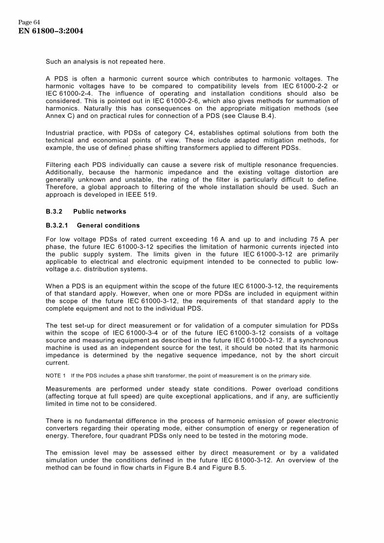
Such an analysis is not repeated here.
A PDS is often a harmonic current source which contributes to harmonic voltages. The harmonic voltages have to be compared to compatibility levels from IEC 61000-2-2 or IEC 61000-2-4. The influence of operating and installation conditions should also be considered. This is pointed out in IEC 61000-2-6, which also gives methods for summation of harmonics. Naturally this has consequences on the appropriate mitigation methods (see Annex C) and on practical rules for connection of a PDS (see Clause B.4).
Industrial practice, with PDSs of category C4, establishes optimal solutions from both the technical and economical points of view. These include adapted mitigation methods, for example, the use of defined phase shifting transformers applied to different PDSs.
Filtering each PDS individually can cause a severe risk of multiple resonance frequencies. Additionally, because the harmonic impedance and the existing voltage distortion are generally unknown and unstable, the rating of the filter is particularly difficult to define. Therefore, a global approach to filtering of the whole installation should be used. Such an approach is developed in IEEE 519.
B.3.2 Public networks
B.3.2.1 General conditions
For low voltage PDSs of rated current exceeding 16 A and up to and including 75 A per phase, the future IEC 61000-3-12 specifies the limitation of harmonic currents injected into the public supply system. The limits given in the future IEC 61000-3-12 are primarily applicable to electrical and electronic equipment intended to be connected to public low-voltage a.c. distribution systems.
When a PDS is an equipment within the scope of the future IEC 61000-3-12, the requirements of that standard apply. However, when one or more PDSs are included in equipment within the scope of the future IEC 61000-3-12, the requirements of that standard apply to the complete equipment and not to the individual PDS.
The test set-up for direct measurement or for validation of a computer simulation for PDSs within the scope of IEC 61000-3-4 or of the future IEC 61000-3-12 consists of a voltage source and measuring equipment as described in the future IEC 61000-3-12. If a synchronous machine is used as an independent source for the test, it should be noted that its harmonic impedance is determined by the negative sequence impedance, not by the short circuit current.
NOTE 1 If the PDS includes a phase shift transformer, the point of measurement is on the primary side.
Measurements are performed under steady state conditions. Power overload conditions (affecting torque at full speed) are quite exceptional applications, and if any, are sufficiently limited in time not to be considered.
There is no fundamental difference in the process of harmonic emission of power electronic converters regarding their operating mode, either consumption of energy or regeneration of energy. Therefore, four quadrant PDSs only need to be tested in the motoring mode.
The emission level may be assessed either by direct measurement or by a validated simulation under the conditions defined in the future IEC 61000-3-12. An overview of the method can be found in flow charts in Figure B.4 and Figure B.5.
Page 64EN 61800−3:2004
Two different operating conditions are defined to cover the different types of PDSs:
– rated input current at base speed in motoring mode (voltage source inverter); – rated torque at 66 % of base speed in motoring mode (thyristor d.c. drive or current source
inverter). NOTE 2 IEC 61800-1 and IEC 61800-2 define base speed as the lowest speed at which the motor is capable of delivering maximum output power. In the case of a voltage source inverter, this is often the same speed as if the motor was fed directly from the mains supply.
For equipment neither covered by IEC 61000-3-2 nor by the future IEC 61000-3-12, (example: rated current above 75 A) recommendations are given in the technical report IEC 61000-3-4 and in Clause B.4.
NOTE 3 Harmonics of the different electrical components of the equipment can be summed using the more exact analytical physical law suitable to the nature of the PDS and to the nature of the other components (see B.3.3).
Page 65EN 61800−3:2004
B.3.2.2 Assessment by simulation
The simulation assessment of individual harmonic emission of a PDS should follow the basic rules summarised in Figure B.4. Characterisation of the PDS and of the voltage source is the starting stage.
Figure B.4 – Assessment of the harmonic emission of a PDS
In the case of high power or medium voltage equipment, the validation of the simulation may be a more complex process than the process described here.
Harmonic emission
assessment
Characterisethe voltage source
and the PDS
Define the voltage source UN : voltage level Uh : voltage distortion level τ : voltage unbalance Z(h) : source impedance RSCe
Define the PDS - type of converter- voltage and current ratings - R SCe min
Define the model for simulationconsidering the PDS and the voltage source characteristics
Test for validation of the modelFor a product range (same type of equipment):one product at or near each end of the range
Simulation
Comparison of resultswithin the toleranceNO
YES
The model is validatedfor the PDSs of the typeat any rating in the range
Proceed to simulationfor defining harmonic emission
with the source under ideal conditionsat nominal voltage, without distortion, unbalance, and
Z(h) = 2πhF1 × LIEC 933/04
Page 66EN 61800−3:2004
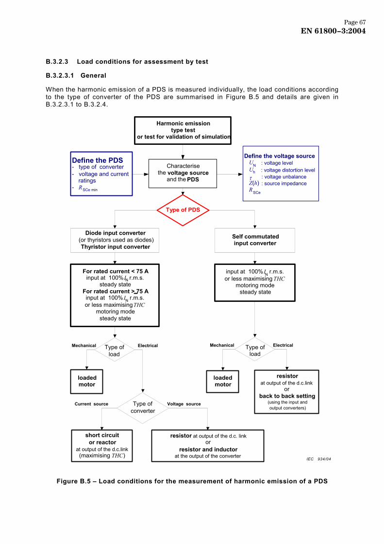
B.3.2.3 Load conditions for assessment by test
B.3.2.3.1 General
When the harmonic emission of a PDS is measured individually, the load conditions according to the type of converter of the PDS are summarised in Figure B.5 and details are given in B.3.2.3.1 to B.3.2.4.
Figure B.5 – Load conditions for the measurement of harmonic emission of a PDS
Harmonic emissiontype test
or test for validation of simulation
Type of PDS
Diode input converter (or thyristors used as diodes) Thyristor input converter
short circuit or reactor
at output of the d.c.link (maximising THC )
resistor at output of the d.c. linkor
resistor and inductorat the output of the converter
Type of load
Type of converter
Self commutated input converter
input at 100% IN r.m.s. or less maximising THC
motoring mode steady state
Type ofload
resistor at output of the d.c.link
or back to back setting
(using the input and output converters)
Mechanical MechanicalElectrical Electrical
loaded motor
Current source Voltage source
loadedmotor
For rated current < 75 A input at 100% I N r.m.s.
steady state For rated current > 75 A i n put at 100% I N r.m.s. or less maximising THC
motoring mode steady state
Characterisethe voltage source
and the PDS
Define the voltage source UN : voltage level Uh : voltage distortion level : voltage unbalance Z(h) : source impedance RSCe
Define the PDS - type of converter - voltage and current ratings - R SCe min
τ
IEC 934/04
Page 67EN 61800−3:2004
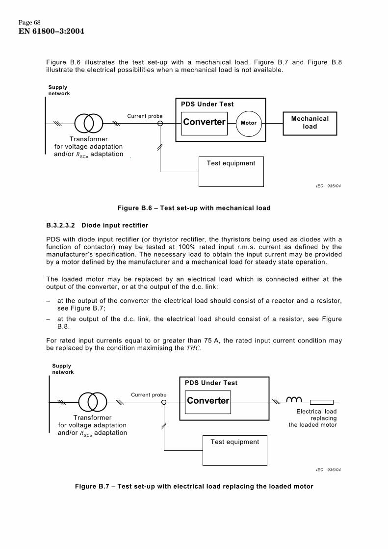
Figure B.6 illustrates the test set-up with a mechanical load. Figure B.7 and Figure B.8 illustrate the electrical possibilities when a mechanical load is not available.
Figure B.6 – Test set-up with mechanical load
B.3.2.3.2 Diode input rectifier
PDS with diode input rectifier (or thyristor rectifier, the thyristors being used as diodes with a function of contactor) may be tested at 100% rated input r.m.s. current as defined by the manufacturer’s specification. The necessary load to obtain the input current may be provided by a motor defined by the manufacturer and a mechanical load for steady state operation.
The loaded motor may be replaced by an electrical load which is connected either at the output of the converter, or at the output of the d.c. link:
– at the output of the converter the electrical load should consist of a reactor and a resistor, see Figure B.7;
– at the output of the d.c. link, the electrical load should consist of a resistor, see Figure B.8.
For rated input currents equal to or greater than 75 A, the rated input current condition may be replaced by the condition maximising the THC.
Figure B.7 – Test set-up with electrical load replacing the loaded motor
Mechanicalload
Transformer for voltage adaptation and/or RSCe adaptation
Supply network
Test equipment
Current probeMotorConverter
PDS Under Test
Transformer for voltage adaptation and/or RSCe adaptation
Supply network
Test equipment
Current probeConverter
PDS Under Test
Electrical loadreplacing
the loaded motor
IEC 935/04
IEC 936/04
Page 68EN 61800−3:2004
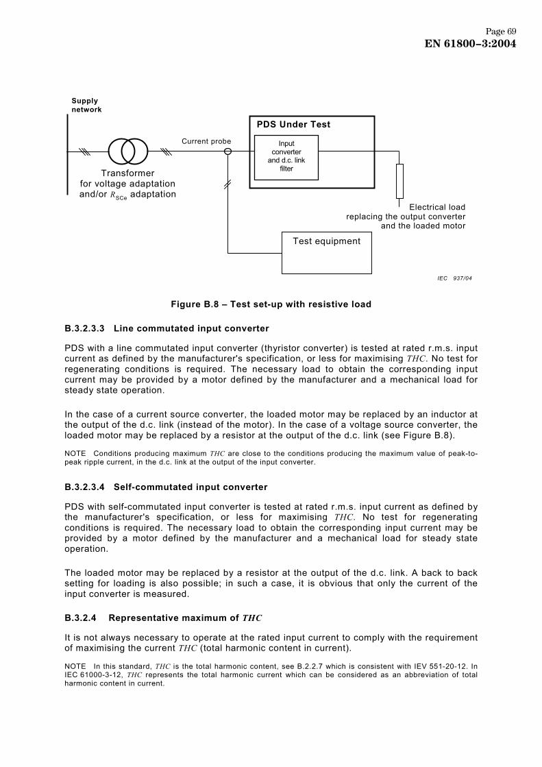
Figure B.8 – Test set-up with resistive load
B.3.2.3.3 Line commutated input converter
PDS with a line commutated input converter (thyristor converter) is tested at rated r.m.s. input current as defined by the manufacturer's specification, or less for maximising THC. No test for regenerating conditions is required. The necessary load to obtain the corresponding input current may be provided by a motor defined by the manufacturer and a mechanical load for steady state operation.
In the case of a current source converter, the loaded motor may be replaced by an inductor at the output of the d.c. link (instead of the motor). In the case of a voltage source converter, the loaded motor may be replaced by a resistor at the output of the d.c. link (see Figure B.8).
NOTE Conditions producing maximum THC are close to the conditions producing the maximum value of peak-to-peak ripple current, in the d.c. link at the output of the input converter.
B.3.2.3.4 Self-commutated input converter
PDS with self-commutated input converter is tested at rated r.m.s. input current as defined by the manufacturer's specification, or less for maximising THC. No test for regenerating conditions is required. The necessary load to obtain the corresponding input current may be provided by a motor defined by the manufacturer and a mechanical load for steady state operation.
The loaded motor may be replaced by a resistor at the output of the d.c. link. A back to back setting for loading is also possible; in such a case, it is obvious that only the current of the input converter is measured.
B.3.2.4 Representative maximum of THC
It is not always necessary to operate at the rated input current to comply with the requirement of maximising the current THC (total harmonic content in current).
NOTE In this standard, THC is the total harmonic content, see B.2.2.7 which is consistent with IEV 551-20-12. In IEC 61000-3-12, THC represents the total harmonic current which can be considered as an abbreviation of total harmonic content in current.
Electrical loadreplacing the output converter
and the loaded motor
Transformer for voltage adaptation and/or RSCe adaptation
Supply network
Test equipment
Current probe Input converter
and d.c. link filter
PDS Under Test
IEC 937/04
Page 69EN 61800−3:2004
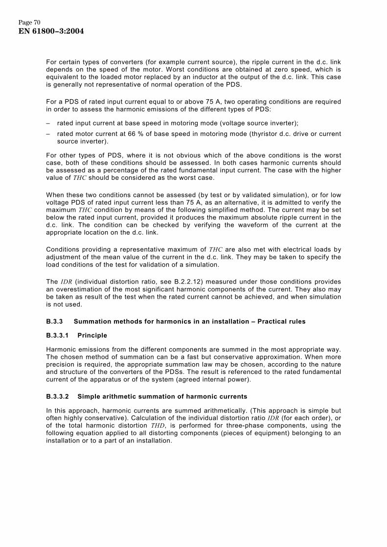
For certain types of converters (for example current source), the ripple current in the d.c. link depends on the speed of the motor. Worst conditions are obtained at zero speed, which is equivalent to the loaded motor replaced by an inductor at the output of the d.c. link. This case is generally not representative of normal operation of the PDS.
For a PDS of rated input current equal to or above 75 A, two operating conditions are required in order to assess the harmonic emissions of the different types of PDS:
– rated input current at base speed in motoring mode (voltage source inverter); – rated motor current at 66 % of base speed in motoring mode (thyristor d.c. drive or current
source inverter).
For other types of PDS, where it is not obvious which of the above conditions is the worst case, both of these conditions should be assessed. In both cases harmonic currents should be assessed as a percentage of the rated fundamental input current. The case with the higher value of THC should be considered as the worst case.
When these two conditions cannot be assessed (by test or by validated simulation), or for low voltage PDS of rated input current less than 75 A, as an alternative, it is admitted to verify the maximum THC condition by means of the following simplified method. The current may be set below the rated input current, provided it produces the maximum absolute ripple current in the d.c. link. The condition can be checked by verifying the waveform of the current at the appropriate location on the d.c. link.
Conditions providing a representative maximum of THC are also met with electrical loads by adjustment of the mean value of the current in the d.c. link. They may be taken to specify the load conditions of the test for validation of a simulation.
The IDR (individual distortion ratio, see B.2.2.12) measured under those conditions provides an overestimation of the most significant harmonic components of the current. They also may be taken as result of the test when the rated current cannot be achieved, and when simulation is not used.
B.3.3 Summation methods for harmonics in an installation – Practical rules
B.3.3.1 Principle
Harmonic emissions from the different components are summed in the most appropriate way. The chosen method of summation can be a fast but conservative approximation. When more precision is required, the appropriate summation law may be chosen, according to the nature and structure of the converters of the PDSs. The result is referenced to the rated fundamental current of the apparatus or of the system (agreed internal power).
B.3.3.2 Simple arithmetic summation of harmonic currents
In this approach, harmonic currents are summed arithmetically. (This approach is simple but often highly conservative). Calculation of the individual distortion ratio IDR (for each order), or of the total harmonic distortion THD, is performed for three-phase components, using the following equation applied to all distorting components (pieces of equipment) belonging to an installation or to a part of an installation.
Page 70EN 61800−3:2004
HD is the generic symbol for IDR or THD. The subscript eq indicates that this value is attached to a particular piece of equipment in the system. The subscript IT indicates that the example is related to a part of an installation, however the same applies to the whole installation (using subscript ST).
SS
HDHDIT
eq
eqeq ×= ∑
In the equation HDeq is referenced to the rated fundamental current of the component (piece of equipment) and HD is referenced to the rated fundamental current of the part of the installation (agreed internal power).
Single-phase components are taken into account by means of an unbalance penalty coefficient:
– for single-phase loads, phase-to-phase, the coefficient is √3:
×
IT
eqeq S
SHD3
– for single-phase loads, phase-to-neutral, the coefficient is 3:
×
IT
eqeq S
SHD3
The penalty coefficient is applied to those terms related to the loads in excess which create the unbalance condition. Example: SIT = 150 kVA
Piece of distorting equipment N°1: Seq = 25 kVA with HD = 65 % , related to its rated current,
HDeq1 = 65 x (25/150)% = 10,8 % , related to ITN1 (or SIT ).
Piece of distorting equipment N°2: Seq = 10 kVA with HD = 10 % , related to its rated current
HD eq2 = 10 x (10/150) % = 0,7 % , related to ITN1 (or SIT ).
Piece of distorting equipment N°3: Seq = 1 kVA with HD = 85 % , related to its rated current,
but single-phase (phase-to-phase), equivalent to 1,73 times its rating as balanced load, with harmonics multiple of three (to be considered),
HDeq3 = 85 x (1,0/150) x 1,73 = 1,0 % related to ITN1 (or SIT).
For the system HD = (10,8 + 0,7 + 1,0) % = 12,5 % with Σ Seq/SIT = (25 + 10 + 1)/150 = 0,240
The calculation should be performed for each harmonic order and for THD.
B.3.3.3 Pseudo-quadratic (variable exponent) summation law
The summation of harmonic currents can be made with a more representative law:
– current known to be in phase (for example diode rectifier), arithmetic summation of each order
Ih = Σi Ihi
– random phase relationship between currents, exponent and summation of each order
αα
1
= ∑
ihih II
α = 1 for h < 5 , and α = 1,4 for 5 ≤ h < 10 , and α = 2 for 10 ≤ h
Page 71EN 61800−3:2004
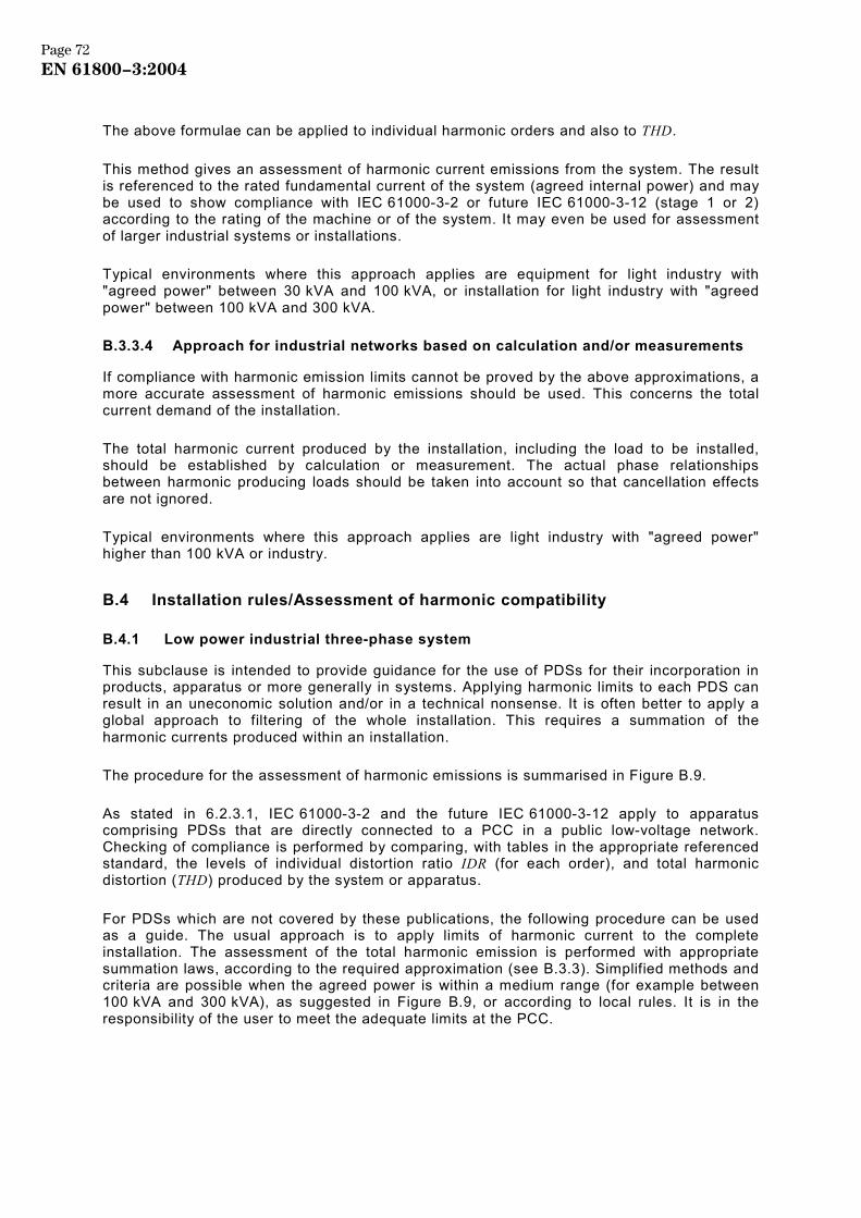
The above formulae can be applied to individual harmonic orders and also to THD.
This method gives an assessment of harmonic current emissions from the system. The result is referenced to the rated fundamental current of the system (agreed internal power) and may be used to show compliance with IEC 61000-3-2 or future IEC 61000-3-12 (stage 1 or 2) according to the rating of the machine or of the system. It may even be used for assessment of larger industrial systems or installations.
Typical environments where this approach applies are equipment for light industry with "agreed power" between 30 kVA and 100 kVA, or installation for light industry with "agreed power" between 100 kVA and 300 kVA.
B.3.3.4 Approach for industrial networks based on calculation and/or measurements
If compliance with harmonic emission limits cannot be proved by the above approximations, a more accurate assessment of harmonic emissions should be used. This concerns the total current demand of the installation.
The total harmonic current produced by the installation, including the load to be installed, should be established by calculation or measurement. The actual phase relationships between harmonic producing loads should be taken into account so that cancellation effects are not ignored.
Typical environments where this approach applies are light industry with "agreed power" higher than 100 kVA or industry.
B.4 Installation rules/Assessment of harmonic compatibility
B.4.1 Low power industrial three-phase system
This subclause is intended to provide guidance for the use of PDSs for their incorporation in products, apparatus or more generally in systems. Applying harmonic limits to each PDS can result in an uneconomic solution and/or in a technical nonsense. It is often better to apply a global approach to filtering of the whole installation. This requires a summation of the harmonic currents produced within an installation.
The procedure for the assessment of harmonic emissions is summarised in Figure B.9.
As stated in 6.2.3.1, IEC 61000-3-2 and the future IEC 61000-3-12 apply to apparatus comprising PDSs that are directly connected to a PCC in a public low-voltage network. Checking of compliance is performed by comparing, with tables in the appropriate referenced standard, the levels of individual distortion ratio IDR (for each order), and total harmonic distortion (THD) produced by the system or apparatus.
For PDSs which are not covered by these publications, the following procedure can be used as a guide. The usual approach is to apply limits of harmonic current to the complete installation. The assessment of the total harmonic emission is performed with appropriate summation laws, according to the required approximation (see B.3.3). Simplified methods and criteria are possible when the agreed power is within a medium range (for example between 100 kVA and 300 kVA), as suggested in Figure B.9, or according to local rules. It is in the responsibility of the user to meet the adequate limits at the PCC.
Page 72EN 61800−3:2004
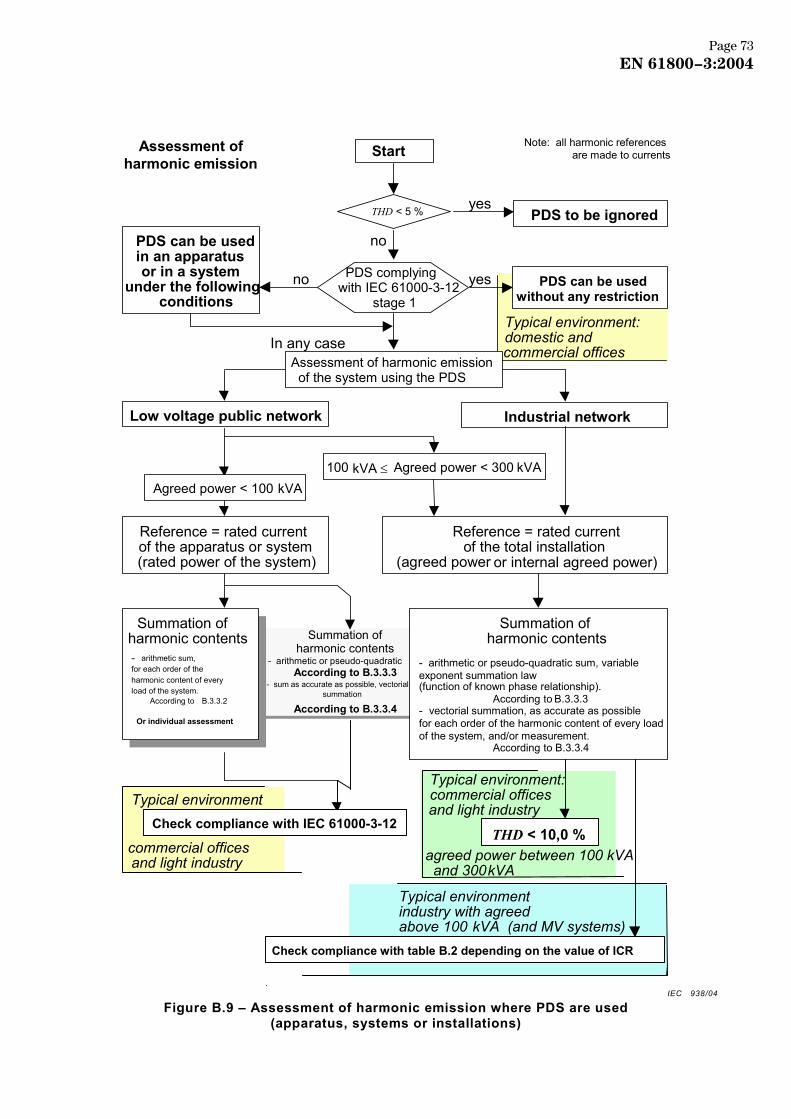
Figure B.9 – Assessment of harmonic emission where PDS are used (apparatus, systems or installations)
Typical environment: commercial offices and light industry
agreed power between 100 kVA and 300 kVA
Summation ofharmonic contents
- arithmetic or pseudo-quadratic sum,
According to B.3.3.3- sum as accurate as possible, vectorial summation
According to B.3.3.4
Summation ofharmonic contents
- arithmetic or pseudo-quadratic According to B.3.3.3
- sum as accurate as possible, vectorial summation
According to B.3.3.4
PDS to be ignored THD < 5 %
PDS complying with IEC 61000-3-12
stage 1
Start
yes
yes
no
no
In any case
Low voltage public network Industrial network
Reference = rated current of the apparatus or system (rated power of the system)
Assessment of harmonic emission
Note: all harmonic referencesare made to currents
Summation harmonic
- arithmetic sum, for each order of the harmonic content of every load of the system.
According to B.3.3.2
Or individual assessment
Summation of harmonic contents - arithmetic sum, for each order of the harmonic content of every load of the system.
According to B.3.3.2
Or individual assessment
Check compliance with IEC 61000-3-12 THD < 10,0 %
Check compliance with table B.2 depending on the value of ICR
Typical environment: domestic and commercial offices
Typical environment
commercial offices and light industry
Typical environment industry with agreed above 100 kVA (and MV systems)
PDS can be used in an apparatus or in a system
under the following conditions
PDS can be used without any restriction
Reference = rated current of the total installation
(agreed power or internal agreed power)
100 kVA ≤ Agreed power < 300 kVA
Summation of harmonic contents
- arithmetic or pseudo-quadratic sum, variable exponent summation law(function of known phase relationship).
According to B.3.3.3 - vectorial summation, as accurate as possible for each order of the harmonic content of every loadof the system, and/or measurement.
According to B.3.3.4
Assessment of harmonic emission of the system using the PDS
Agreed power < 100 kVA
IEC 938/04
Page 73EN 61800−3:2004
B.4.2 Large industrial system
B.4.2.1 Principles
This subclause is intended to provide guidance for the use of PDSs for their incorporation in systems. Applying harmonic limits to each PDS can result in an uneconomic solution and/or in a technical nonsense. It is often better to apply a global approach to filtering of the whole installation. This requires a summation of the harmonic currents produced within an installation.
The procedure for the assessment of harmonic emissions is summarised in Figure B.9.
The technical report IEC 61000-3-6 should be applied directly for installations supplied by a medium voltage power supply network, which is the case for large PDSs and particularly those of rated voltage above 1000 V a.c.
It is usual to separate the installation into different parts according to natural decoupling devices (transformers, etc.). The separation should result from the analysis of the complete network, taking possible resonances into account. (see Figure B.2).
The location of required filters should be carefully established, but it is evident that filtering each PDS is not practicable.
The usual approach is to apply limits of harmonic current to the complete installation, or to parts of the installation as seen above. In critical cases, a more detailed analysis involving the existing level of voltage harmonic distortion is used.
B.4.2.2 Current distortion method for complete installation
In this approach harmonic current limits are applied to the whole installation. Limits are applied both to individual distortion ratios (IDR) for individual orders and to THD.
The harmonic currents of the total installation should be in accordance with the following Table B.2 at the defined point of coupling. See definition of RSI in B.2.3.6. The PDS supplier and customer should agree on the point of coupling (PCC or IPC) and on the applications of other emission limits coming from local regulations. The point of coupling should be an identified bus bar.
NOTE From the definition of RSI, dedicated to a defined bus bar, it is clear that all loads fed from this bus bar contribute to the definition of the corresponding current (ITN) to be taken into account for calculation of harmonic emission.
In the USA, IEEE 519 applies this approach at all voltage levels for electricity distribution networks. Table B.2 gives an example of practical limits already experienced in North America.
Harmonic currents are expressed as percentages of the total current corresponding to the internal agreed power of the a.c. supply of the total installation (IDR). In the case of a PCC, the load current is defined by the “agreed power”, as agreed between the user and the utility. In the case of an IPC, the rated fundamental load current is equal to the rated load current of the feeder to the IPC. See B.2.3.5 and B.2.3.6.
Page 74EN 61800−3:2004
Table B.2 – Harmonic current emission requirements relative to the total current of the agreed power at the PCC or IPC
Individual distortion ratio IDR
RSI h < 11 11 ≤ h < 17 17 ≤ h < 23 23 ≤ h < 35 35 ≤ h TDR
RSI < 20 4 % 2 % 1,5 % 0,6 % 0,3 % 5 %
20 ≤ RSI < 50 7 % 3,5 % 2,5 % 1 % 0,5 % 8 %
50 ≤ RSI < 100 10 % 4,5 % 4 % 1,5 % 0,7 % 12 %
100 ≤ RSI < 1000 12 % 5,5 % 5 % 2 % 1 % 15 %
1000 ≤ RSI 15 % 7 % 6 % 2,5 % 1,4 % 20 %
Even harmonics are limited to 25 % of the odd harmonics.
For systems with a pulse number (= q) higher than 6, the limits for each individual harmonic are increased by the factor 6/q . This corresponds for a 12 pulse system to 2 . The THD limit remains unchanged.
B.4.2.3 Case by case analysis
As an alternative, a complete analysis of the system can be conducted, and should be conducted in critical cases. The results of the analysis can then be used to correctly define the total filtering, or other mitigation methods.
The following procedure should be adopted:
– assess the existing level of harmonic voltage distortion at the PCC (at the responsibility of the operator of the distribution network – public or private);
– calculate or measure the harmonic impedance of the supply at the PC (at the responsibility of the operator of the distribution network – public or private if PCC, and the responsibility of the user if IPC – internal point of coupling); IEC 61000-2-6, Clause A.2 gives information on the harmonic impedance encountered in networks;
– calculate or measure harmonic currents that the PDS to be connected is going to inject into the system (at the responsibility of the manufacturer);
– calculate harmonic voltages that can result from this (at the responsibility of the user).
NOTE All the rules and methods listed in the technical specification IEC 61000-3-6, although defined for medium voltage (from 1 kV up to and including 35 kV) or high voltage (> 35 kV) public networks, are applicable to industrial networks, including their low voltage parts.
In the case of a PCC, the resulting harmonic voltages should not exceed the planning levels defined by the utility. In the case of an IPC, the resulting harmonic voltages should not exceed the compatibility levels.
Compatibility levels for harmonic voltages are defined by IEC 61000-2-2 on low voltage public systems, by IEC 61000-2-12 on medium voltage public systems and by IEC 61000-2-4 on private industrial systems.
At the PC an available nominal power (called agreed internal power) can be defined. In the case of a PCC this is the “agreed power” (see B.2.3.4 and B.2.3.5). A disturbance allowance can be allocated to the PDS to be connected. The reasonable solution consists of defining this disturbance allowance proportional to the ratio of the PDS's rated power to the agreed internal power at the PC, and proportional to compatibility levels defined by standards quoted above.
Page 75EN 61800−3:2004
B.4.2.4 Telephone interference
In North America and Finland, the parallel construction of energy distribution and telephone lines has led to the introduction of TIF (telephone interference factor). IEEE 519 (1992), clause 6.8, presents the result of a weighting of the various harmonics.
The equivalent psophometric current is defined as Ip = I × TIF
and the local recommended practices require that Ip < IpA
Within the installation, the common mode harmonic emission on the motor cable can cause interference with telephone lines if they are running in parallel. This should be avoided (see 6.2.5).
B.4.3 Interharmonics and voltages or currents at higher frequencies
In this frequency range, above harmonic order 40 and up to 9 kHz, the PDS should be considered as a voltage source emitter. There are no emission requirements for PDSs until compatibility levels will be standardised.
However, application of certain types of PDSs can require the consideration of the emission of interharmonics or of currents or voltages at higher frequencies (up to 9 kHz). This is mainly the case for high power PDSs such as cyclo-converters or current source inverters. This can also be the case for active front-end converters where the PWM switching is directly coupled to the network.
Interharmonics at frequencies slightly different from the fundamental or from predominant harmonics can also cause voltage fluctuations (see B.6.2). They result from beat frequencies which can be seen on non-linear systems such as lighting (function of the square of the voltage). The non-linear response of the disturbed equipment causes the sum and difference of the different harmonic or interharmonic frequencies to appear. The difference frequency can be in the range that causes flicker. The main origin is cyclo-converters or current source inverters. This case is covered by compatibility levels given in IEC 61000-2-4.
Interharmonics can directly affect power factor correction capacitor banks and harmonic filters, particularly due to resonances.
The emission should be limited to 80 % of the indicative voltage levels below (from Annex C of IEC 61000-2-4 (2002)).
u = 0,2 % for class 2 IPCs; u = 1 % for class 3 IPCs; ub = 0,3 % for class 2 IPCs; ub = 1,5 % for class 3 IPCs;
where "u" is the ratio of the r.m.s. voltage at that frequency to the r.m.s. value of the fundamental component of the voltage, and "ub" is the level related to any 200 Hz bandwidth centred at frequency F, and expressed as follows:
∫+
−
×××=Hz100
Hz100
2
N1b )(
Hz20011 F
F
dffVV
u
Page 76EN 61800−3:2004
where V1N is the rated r.m.s. value of the fundamental component; V(f) is the r.m.s. voltage at frequency f; F is the centre frequency of the band (the band is above the 40th harmonic).
At higher frequencies, the origin is mainly from active front-end converters where the PWM switching is strongly coupled to the network.
B.5 Voltage unbalance
B.5.1 Origin
Voltage unbalance on a three-phase system is generally caused by unequal loading on two of the three phases by single-phase loads. The voltage unbalance is directly related to the amount of the single-phase load as a percentage of the rating, and to the impedance of the mains supply. As an example, consider a three-phase transformer with a defined regulation, and only a single-phase load connected between two phases. If the load is a significant percentage of the kVA rating of the transformer, the output voltages (phase to neutral) of the two phases connected to the load will be reduced while the third winding without any load will remain the same.
Significant unbalance on transformers will cause excessive heating. The manufacturer should be consulted to determine if the transformer is capable of supplying single-phase loads that are a significant percentage of its rated kVA capacity.
Other three-phase loads connected to an unbalanced three-phase source of power are generally affected in a detrimental manner. As an example, the unbalance will cause a reverse sequence current to flow in a three-phase induction motor, which will reduce the torque output at rated current or cause excessive heating at rated output of the motor. In some motors, an unbalance of 3 % can result in a 10 % derating of their output. If an unbalance condition exists on the mains supplying a three-phase motor, it is important to consult the motor manufacturer to determine the proper derating for safe operation.
B.5.2 Definition and assessment
B.5.2.1 Definition
Voltage unbalance is defined in IEC 61000-2-2, IEC 61000-2-4 or IEC 61000-2-12. Some methods of calculation are given below.
In a polyphase system, voltage unbalance is a condition in which the r.m.s. values of the fundamental component of the line-to-line voltages, or the phase angle between consecutive phases, are not all equal. For the purposes of this standard, the degree of that inequality is expressed as the ratio of the negative sequence component to the positive sequence component.
In some circumstances, the zero sequence component should be included in the assessment of voltage unbalance.
B.5.2.2 Complete analysis
The accurate definition relates to symmetrical component analysis of the three-phase system. This type of analysis is based on the concept that any phase voltage deviation from the ideal three-phase system can be described by the addition of three vectors. They are called the zero, positive and negative sequence vectors and are defined as follows.
Page 77EN 61800−3:2004
UA = UA0 + UA1 + UA2 phase A voltage
UA0 = (UA + UB + UC)/3 zero sequence component
UA1 = (UA + a UB + a2 UC)/3 positive sequence component
UA2 = (UA + a2 UB + a UC)/3 negative sequence component
where UA , UB , and UC are the phase voltage vectors and "a" is the operator,
a = – (1/2) + j (√3/2 ).
The ratio of the negative sequence to the positive sequence voltage is the voltage unbalance. This is as follows:
τ % = 100 U2/U1
Example 1: Amplitudes and phase angles of line-to-neutral voltages are known allowing the line-to-line voltages and the corresponding phase angles to be calculated.
UAN = 231,00 and 0,0°, UBN = 220,00 and –125,1°, UCN = 215,00 and 109,8°
UAB = 400,32 and 26,7°, UBC = 386,00 and –98,0°, UCA = 364,98 and 146,3°
resulting in U0 = 22,36 35,2°, U2 = 20,40 and 90,7°, U1 = 383,51 and –5,0°
and voltage unbalance: τ = 100 ( 20,36/383,51 ) = 5,320 %, with a zero sequence component of 5,831 %.
Example 2: Amplitudes and phase angles of line-to-neutral voltages are known allowing the line-to-line voltages and the corresponding phase angles to be calculated:
UAN = 230,00 and 0,0°, UBN = 280,00 and –135,0°, UCN = 170,00 and 130,0°
UAB = 471,50 and 24,8°, UBC = 339,94 and –105,1°, UCA = 363,40 and 159,0°
resulting in U0 = 59,34 and –138,8°, U2 = 85,79 and 48,1°, U1 = 386,40 and –3,7°
and voltage unbalance: τ = 100 ( 85,79/386,40 ) = 22,230 %, with a zero sequence component 15,356 %.
B.5.2.3 Approximate method
Three approximations are given below. The first one usually provides the best results, with an error less than 5 % for any kind of unbalance for which the line-to-neutral voltages have phase angles within a tolerance of ±15°, and the amplitude within a tolerance of ±20 % compared to the corresponding ideal balanced system (positive sequence or negative sequence).
U12, U23 and U31 are the three line-to-line voltages, with δij = (Uij – Uaverage)/(3 × Uaverage) for each of the three line-to-line voltages, and τ the voltage unbalance as the ratio of the negative sequence voltage amplitude to the positive sequence voltage amplitude,
∑≈3
1
2ij6 δτ
The much more simple approximation:
−×
≈
average
minmaxU
UU32τ
provides acceptable results (absolute error generally less than 1 %) for τ up to 7 %.
Page 78EN 61800−3:2004
The formula proposed by NEMA, also gives acceptable results (absolute error generally less than 1 %) for τ up to 10 % or where phase shifts are large:
average
averageij
U
UUMAX −≈τ
Example 1, as above:
UAN = 231,00 UBN = 220,00 and UCN = 215,00
UAB = 400,32 UBC = 386,00 and UCA = 364,98
Uaverage = (400,32+386,00+364,98)/3 = 383,77 and without decimals Uaverage = (400+386+365)/3= 383,66
δ12 = 1,432 % δ23 = 0,197 % δ31 = –1,629 %
The voltage unbalance is [6(1,4322+0,1972+1,6292)]1/2 = 5,3 %
or (2/3) × (Umax – Umin)/Uaverage = (2/3) × (400 – 365)/383,7 = 6,1 %, or using the last approximation: 18,7/383,7 = 4,9 %.
Example 2, as above:
UAN = 230,00 UBN = 280,00 and UCN = 170,00
UAB = 471 UBC = 340 and UCA = 363
Uaverage = (472+340+363)/3 = 391,7
δ12 = 6,801 % δ23 = –4,397 % δ31 = –2,404 %
The voltage unbalance is [6(6,8012 + 4,3972 + 4,3972)]1/2 = 20,7 %
or (2/3) × (Umax – Umin)/Uaverage = (2/3) × (472 – 340)/391,7 = 22,4 %, or using the last approximation: 80,3/391,7 = 20,5 %.
B.5.3 Effect on PDSs
The effect on the PDS will vary depending on the type of power circuit and control method used. Each type of control and circuit should be analysed in detail. Generally, the effect will be small on controlled or uncontrolled converters that supply resistive loads. Phase controlled converters of the type that use phase shifted line voltage for their reference will be affected less than converters that use a voltage ramp synchronised to the line using zero crossings for their reference. Controlled or uncontrolled converters that supply capacitor banks, used in the d.c. loop of indirect converters (voltage source inverters), will have current unbalances that are significantly larger than the voltage unbalance and larger than converters that supply an inductive load such as a d.c. motor.
Special care should be taken with the design of converters that supply capacitor banks since the peak current is greatly magnified by the voltage unbalance. For very large capacitor banks where the ripple voltage is small, the peak current from each phase is limited only by the source impedance and any additional impedance in the PDS and the difference between the capacitor bank voltage and the line voltage. The ratio of peak currents between phases can be as large as 20 % for 3 % voltage unbalance with a 1 % source impedance. Fortunately, this is an extreme condition since it is unlikely that single-phase loading could cause this magnitude of unbalance with a 1 % source impedance.
Page 79EN 61800−3:2004
B.6 Voltage dips – Voltage fluctuations
B.6.1 Voltage dips
B.6.1.1 Definition
Perhaps the most common form of low-frequency disturbance is the voltage dip or a reduction of voltage on one or all of the three phases. A voltage dip is a sudden reduction of the voltage at a point in the electrical system, followed by voltage recovery after a short period of time, from half a cycle to a few seconds. A voltage dip is generally caused by the clearing of faults by the utility supplying the mains or by the starting of large motors in or near the user's location. Surveys by different utilities in different countries have shown that voltage dips can range from a time of half a cycle to 15 cycles or more at voltages outside the 10 % voltage tolerance. The residual voltage (lowest value of the voltage during the dip) is now preferred to the depth of the dip to characterise the magnitude (the depth is the difference between the reference voltage and the residual voltage). The residual voltage largely depends on the relative location of the voltage source (generally a high voltage/medium voltage substation), the event equivalent to a short circuit and the observation point. Comprehensive information is available in IEC 61000-2-8.
B.6.1.2 Effect on PDSs
B.6.1.2.1 Fundamentals
Voltage dips can have detrimental effects upon the performance of PDSs. When the supply voltage is reduced, usually the power that can be transferred from the mains to the motor is also reduced. However, some PDS converters compensate for voltage dips over limited ranges by changing control angles for input rectifiers. Also of concern, regenerative converters that transfer mechanical power from the motor back to the mains may encounter issues with voltage dips.
The effect of voltage dips on PDS should be considered according to the physical nature of the driven equipment. Moreover, the electronic control of the PDS and the power converter components have to be distinguished (see the technical report IEC 61000-2-8).
The control part could be immune, with performance criterion A, to certain types of dips, and this could be of no use unless it is consistent with the behaviour of the converter or of the driven equipment. The converter has no energy storage capability. The driven equipment generally has little energy storage capability, which can be used under certain conditions. To claim that a PDS is immune to voltage dips purely on the basis of the immunity of the control part would be misleading. The use of a specific sequence in the control should be documented to make it possible for the user to define the suitable adaptation to the driven equipment.
B.6.1.2.2 Controlled converters
Controlled converters, such as those that are made up of thyristors, GTOs (gate turn off thyristor), or transistors, are generally used to convert the a.c. mains to a variable d.c. voltage. The logic that is used to synchronise the control of the power semiconductors is often designed to inhibit rectification when the mains voltage drops below a specific value. In some cases, the control is shut off until the user resets the logic or, in others, operation will be resumed only if the voltage returns within a specified amount of time. Normally, the PDS will not be able to control the motor during the dip interval and control could be lost until the logic is reset. If the process that the PDS is controlling is critical, discussions with the PDS manufacturer should occur such that the reaction of the logic to the voltage dip is compatible with the process needs. In some critical cases, it is necessary to apply additional measures (for example alternative power sources) to carry the process through severe voltage dips.
Page 80EN 61800−3:2004
During voltage dips, the power available from the BDM/CDM and to the motor is reduced. This can affect operation depending on the motor operating points. Consider the case of a controlled 6-thyristor bridge supplying power to a d.c. motor. If the motor is running at high speed, a voltage dip can cause the peak line voltage to drop below the armature voltage. The thyristors will be commutated off by the armature circuit and the current in the armature circuit will be reduced. If on the other hand, a voltage dip occurs when the motor is running at low speed, the control circuitry can advance the control point to compensate for the reduced voltage. In this case, the control of the motor will not be affected. For critical loads, the effect of a voltage dip should be discussed with the manufacturer of the PDS to determine how the control circuitry will react.
Regenerative converters of the type that use the line voltage to commutate the thyristors in the bridge are particularly sensitive to voltage dips. If the line voltage drops too low during this reverse power flow, control of the power flow from the motor to the mains is lost since the thyristors cannot be turned off. If the control circuitry does not react or if the dip is particularly abrupt or occurs after a thyristor is turned on, the previously conducting thyristor cannot be turned off and excessive uncontrolled currents can flow from the motor. These currents can result in potentially detrimental effects on the process or even damage to the motor. For critical loads, the effect of voltage dips on regenerative converters should be discussed with the manufacturer of the PDS to determine how the control and power circuits will react during this interval. For critical loads, additional circuitry can be added to force-commutate the thyristors or alternative power sources can be used to carry the PDS through the dips.
Regenerative converters of the type that are force commutated by some means can also be affected by voltage dips. This is because the reduction in voltage during the dip can reduce the amount of power that can be transferred from the load to the motor and to the mains. If this condition exists, control of the motor can be lost during this interval.
B.6.1.2.3 Uncontrolled converters
Uncontrolled converters such as diode bridges are not greatly affected by a voltage dip, with the exception of the high inrush currents which can flow into the capacitor banks of voltage source converters after the voltage reappears. However, their output power and voltage are reduced during the voltage dip. This can cause detrimental effects on other parts of the PDS. If, for example, the converter is supplying power to an inverter, the output voltage of the inverter will be limited and control of the a.c. motor will be lost.
Some manufacturers also inhibit operation when the voltage feeding the inverter drops below a specific value. Some designs also require that the logic be reset before operation can continue. Other designs will restart operation when the voltage returns, but control of the motor is lost during the interval that the logic is inhibited. This interval can be extended by the time needed to synchronise the inverter control logic with the actual speed of the motor after control is lost.
The synchronisation is needed to match the output frequency of the inverter to the actual speed of the motor. The synchronisation process determines the appropriate frequency and voltage that should be applied to the motor for smooth transition from coasting to control.
PDSs of the type that would have a very large capacitor bank could ride through short voltage dips because of the energy stored in the capacitor bank. Generally, it is not economical to make a capacitor bank large enough to operate through voltage dips. In the case of critical loads, a battery can be used to supply power during the voltage dip. PDSs with adapted control can be able to continue operation during voltage interruption, provided the output power is near zero. In all cases, the effects of voltage dips on the operation of the PDS should be discussed with the manufacturer to determine if the PDS is compatible with process needs.
Page 81EN 61800−3:2004
B.6.1.2.4 General protection types
It has been shown that immunity to voltage dips is very dependent on the nature of the converter and on the load behaviour. Absolute protection can be very expensive, and the choice of the protection should be carefully compared with the process requirements.
Absolute protection requires a back up power supply. For example, this can be a UPS (uninterruptible power system), external to the PDS, or a d.c. source (battery) supplying the d.c. link of a voltage source inverter.
Ridethrough sequence is a technique which uses the possibilities of the command to avoid transient overcurrent, but without backup energy. Therefore, the speed of a passive load will necessarily decrease with a rate approximately given by the ratio of the load torque to the inertia. For safety reasons, this kind of protection cannot be used with active loads (example of hoisting during regeneration where mechanical braking is necessary).
Flying restart is the continuation of the ridethrough sequence which can be used in case of passive loads with long or very long coast down times. This can also be a protection against dips or short interruptions.
Automatic restart always implies safety conditions, which are the responsibility of the user.
B.6.2 Voltage fluctuation
Interharmonics can cause flicker on lighting equipment, as explained in B.4.3 and compa-tibility levels are given in IEC 61000-2-2, in IEC 61000-2-4, in IEC 61000-2-12 according to the type of network. Interharmonic emission of a PDS should be limited in such a way that the calculated interharmonic voltage at the IPC, due to a given PDS, does not exceed 80 % of the voltage compatibility levels.
PDSs driving large loads such as punch presses, flying saws, and machine tools will require large currents from the mains periodically. This will cause voltage fluctuations of the mains voltage. The source impedance of the mains supplying these PDSs should be sized so that the voltage fluctuation does not exceed the 10 % tolerance.
Peak loads that on average do not exceed the ratings of the supply system, but will produce deviations of the supply voltage that exceed the tolerance should also be considered when sizing this impedance. On the public network, the voltage fluctuation from a single piece of equipment is not supposed to exceed 3 %. If fluctuations are frequent, flicker limits have to be applied to the public network and to any network which supplies a lighting load (see 6.2.4).
B.7 Verification of immunity to low frequency disturbances
According to 5.2.1, the immunity of the PDS to low frequency phenomena may be verified by calculation, simulation or test. The manufacturer can use the cells of Table B.3 to identify which verification method has been used for each phenomenon.
Page 82EN 61800−3:2004

Table B.3 – Verification plan for immunity to low frequency disturbances
Phenomena Calculation Simulation Test Analysis Not applicable
Harmonics
Commutation notches
Voltage variations
Voltage changes
Voltage fluctuations
Voltage dips
Voltage unbalance
Frequency variations
Supply influences – Magnetic fields
Page 83EN 61800−3:2004
Annex C (informative)
Reactive power compensation – filtering
C.1 Installation
C.1.1 Usual operation
A user of electricity, supplied by a distribution network, generally has several or many apparatuses finally connected at the same PCC. The term "installation" is used to describe the combination of apparatus, equipment or systems and their feeding systems which are connected at the PCC.
In the same way, many industrial apparatuses include more than a single PDS.
A discussion of power factor, reactive power and harmonic emission of a single PDS is not sufficient and can cause unnecessary technical difficulties. In reality, the solution which is required is a solution for the installation. The installation contains many different loads.
Under steady state conditions at any point of a three-phase a.c. network, the line-to-neutral voltage and the line current are periodic quantities, of period T, and frequency f = 1/T. The voltage and current are rarely without phase shift and they include harmonics which distort their pure sinusoidal waveforms. However, electrical energy is distributed by means of voltage sources, so at any point of a supply (supply of a converter or supply of an industrial installation), the current waveform is more distorted than the voltage waveform. Therefore, for calculation of active and reactive power, it is reasonable to assume that at any point of the network, the voltage is a pure sinusoidal wave whose root mean square value (line-to-neutral) equals V. Calculation of the active power P, on a single-phase is defined by
∫=T
ttitvT
P0
d )( )(1
which can be simplified and gives:
( )11 cos ϕIVP =
where I1 is the root mean square of the fundamental component of the line current;
ϕ1 is the phase shift between the fundamental component of the current and the line-to-neutral voltage.
P is conventionally positive when the current I has a phase shift of less than π/2 relative to the voltage, (with voltage in volts and current in amps give the power in watts). With the same assumptions, the reactive power Q expressed in reactive volt amps [var] is defined by
( )11 sin ϕIVQ =
Page 84EN 61800−3:2004
This quantity shows evidence of reactive elements such as reactors or capacitors inside the industrial installation. It is said that those components are consumers of reactive power when the quantity Q is positive (reactors) or are producing reactive power when the quantity Q is negative (capacitors).
Similarly, the apparent power S (in volt amps [VA]) at a point of the network is defined as the product of the root mean square of voltage (line-to-neutral) and line current:
1IVS =
On a three-phase network, the active power, the reactive power and the apparent power are the sums of the corresponding power on each phase, which gives for a balanced system:
P = 3 V I1 cos (ϕ1) = 3 U I1 cos(ϕ1)
Q = 3 V I1 sin (ϕ1) = 3 U I1 sin(ϕ1)
S = 3 V I = 3 U I
with U, root mean square of the line-to-line voltage.
The power factor λ is defined as the ratio of the active power to the apparent power and is expressed in single-phase and three-phase as well with the following equation:
)cos( 11 ϕλ
II=
SP=
This fundamental equation shows that the power factor depends on both displacement factor and harmonic content of the current.
As a summary, the fundamental assumption which is stated is that the voltage is considered as a pure sinusoidal waveform and the current is distorted. This assumption is made for the calculation of power and all the consequences such as power factor. For other calculations, such as harmonic voltage distortion contribution of a load, the internal impedance of the network should be considered. The voltage distortion contribution of this load can be calculated from the distorted current flowing at this point and the internal impedance seen from this point.
C.1.2 Practical solutions
C.1.2.1 Common practice
It is well-known that to avoid overrating of the installation and an unnecessary increase of the current flowing in the distribution network, it is necessary to work with a good power factor. But practical use considered this power factor only from the reactive power point of view, in fact it has been seen here that harmonic content is also concerned.
It has usually been the case that an industrial installation consumes reactive power. Therefore, it has also been usual to install a global compensation in order to reduce the displacement factor and so reduce the installation's consumption of reactive power. In order to do that, capacitors were installed whether close to the consumer of reactive power, or globally close to the PCC. In some countries, utilities introduce taxes for that displacement factor, particularly when the distribution network is heavily used.
Page 85EN 61800−3:2004
C.1.2.2 Evolution of common practice
Because power factor is of concern and because of increasing use of distorting loads, harmonic compensation is also necessary. This harmonic compensation can be performed globally with filtering of the complete installation or locally with filters close to the distorting loads. It can also be better to use non-polluting loads.
From this introduction, it can be seen that two types of compensation are necessary: displacement factor and current harmonic content. Two methods can be used for each of these compensation types: a global approach for the total installation or a local approach for each distorting load. Four cases can be seen, but none is independent so this problem has to be discussed in more detail.
C.1.3 Reactive power compensation
C.1.3.1 General compensation criteria
Power factor correction equipment is composed of capacitor banks connected to the power line by electromechanical or static contactors. The following covers phenomena related by use of capacitor banks connected by electromechanical contactors.
The size of the capacitor bank to be installed is a function of the active and reactive power compensation needed by the system, and also of their variation during the day (load-time characteristics). It is also a function of the pricing practice of the utility.
The correction is frequently defined with the mean value of energy consumption (active and reactive) during the heavy duty times of the day, within a one month period.
NOTE The concept of reactive energy used in this annex is defined by the time integral of the reactive power.
For rating, it is necessary to know the utility criteria:
– heavy duty times in a day,
– limits of reactive power ratio free of charge (for example tan ϕ), – user data such as load-time characteristic.
It can be seen that correction of reactive power consumption cannot be constant nor permanent. A permanent correction would actually lead to reactive power injection in the supply network at certain times. The result would be an increase of the voltage in the user's installation which is not necessarily an advantage. Such a study is of concern for a complete installation and almost impossible for each PDS.
Another point is that capacitors can be installed either on the low-voltage side or on the medium-voltage side. Common practice shows that the installation on the MV side has an economical advantage, as soon as reactive power correction reaches 600 kvar. For lower ratings the LV side should be preferred.
If power factor correction capacitors are to be installed in networks with harmonic current sources, it is recommended that reactors should be added in series with the capacitors. This is so that the resulting resonance frequencies are shifted below the lowest frequency of the characteristic harmonics, normally the 5th (see C.1.3.4).
Page 86EN 61800−3:2004
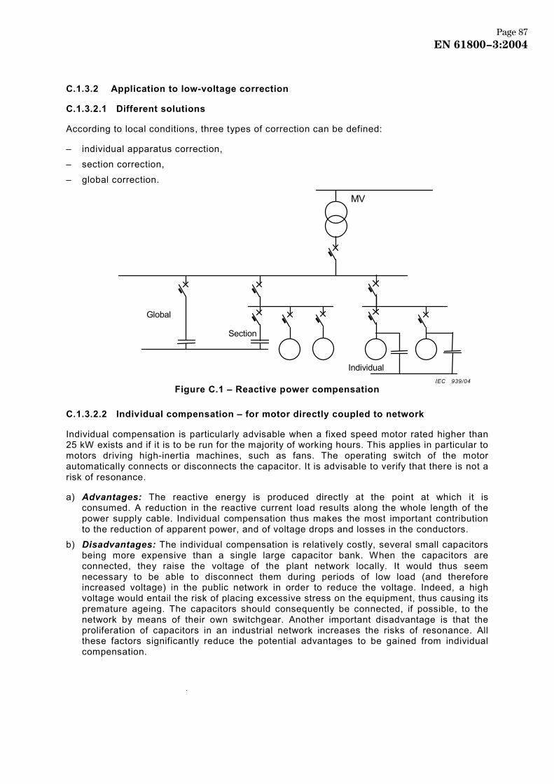
C.1.3.2 Application to low-voltage correction
C.1.3.2.1 Different solutions
According to local conditions, three types of correction can be defined:
– individual apparatus correction, – section correction, – global correction.
Global
Section
Individual
MV
Figure C.1 – Reactive power compensation
C.1.3.2.2 Individual compensation – for motor directly coupled to network
Individual compensation is particularly advisable when a fixed speed motor rated higher than 25 kW exists and if it is to be run for the majority of working hours. This applies in particular to motors driving high-inertia machines, such as fans. The operating switch of the motor automatically connects or disconnects the capacitor. It is advisable to verify that there is not a risk of resonance.
a) Advantages: The reactive energy is produced directly at the point at which it is consumed. A reduction in the reactive current load results along the whole length of the power supply cable. Individual compensation thus makes the most important contribution to the reduction of apparent power, and of voltage drops and losses in the conductors.
b) Disadvantages: The individual compensation is relatively costly, several small capacitors being more expensive than a single large capacitor bank. When the capacitors are connected, they raise the voltage of the plant network locally. It would thus seem necessary to be able to disconnect them during periods of low load (and therefore increased voltage) in the public network in order to reduce the voltage. Indeed, a high voltage would entail the risk of placing excessive stress on the equipment, thus causing its premature ageing. The capacitors should consequently be connected, if possible, to the network by means of their own switchgear. Another important disadvantage is that the proliferation of capacitors in an industrial network increases the risks of resonance. All these factors significantly reduce the potential advantages to be gained from individual compensation.
IEC 939/04
Page 87EN 61800−3:2004
C.1.3.2.3 Compensation by section
In the case of compensation by section, a single bank of capacitors, operated by means of its own switchgear, compensates a group of consumers of reactive energy located in a workshop or in an area.
a) Advantages: The compensation by section requires less investment than individual compensation. However, the load curves should be well-known in advance to enable correct sizing of the batteries of capacitors and to avoid the risks of overcompensation (when the reactive power supplied is greater than that required), which produces permanent overvoltages, leading to premature ageing. The bank of capacitors have their own switchgear, thus making it easy to disconnect them during periods of low loads on the public network, even when the corresponding power consumers remain connected.
b) Disadvantages: The power supply cables of the various power consumers have to be sized to carry both the reactive and active currents. In addition, provision should be made to protect the capacitors (for example fuses, circuit-breakers, etc.), and discharge them for safety purposes (discharging resistors) during maintenance operations. The fuses should also be regularly monitored.
C.1.3.2.4 Global compensation
In the case of global compensation, the production of reactive energy is concentrated at a single point, most frequently in the substation, or in an area which is sufficiently large and well-ventilated. In installations which have only small power consumers, it is generally advisable to adopt automatically controlled central compensation, again so as to avoid overcompensation. Where the load curve shows little fluctuation, it is necessary merely to engage the whole battery during the periods of operation of the installations.
a) Advantages: The capacitors have a good utilisation factor, and the installation is easier to monitor. In addition, with automatic control by the capacitor bank, the load curve of the plant can be followed effectively, while avoiding manual intervention (i.e. manual engaging and disengaging). This solution is potentially beneficial from an economic point of view if the load variations are not attributable to specific power consumers.
b) Disadvantages: The installations downstream of the global compensation connection carry all of the reactive power.
C.1.3.3 Application to medium-voltage correction
Compensation is generally carried out on a centralised basis. The capacitors are grouped in banks in the medium-voltage substation. The banks are connected to the medium-voltage bus via a circuit-breaker. Their power can reach several megavars (Mvar), and they can be divided into smaller sections which are brought into operation successively in order to obtain optimum compensation as a function of the daily load curve. Each section is operated by a switch provided for this purpose as a function of daily load curve or on-line control.
a) Advantages: When the banks of capacitors have power levels greater than 600 kvar, the cost of medium voltage compensation is typically less than that of low-voltage compensation.
b) Disadvantages: This method of compensation provides no relief to the part of the network which is located downstream of the capacitors. Engaging the capacitor bank causes voltage transients. Operation requires more attention than with capacitors in the low-voltage section.
Page 88EN 61800−3:2004
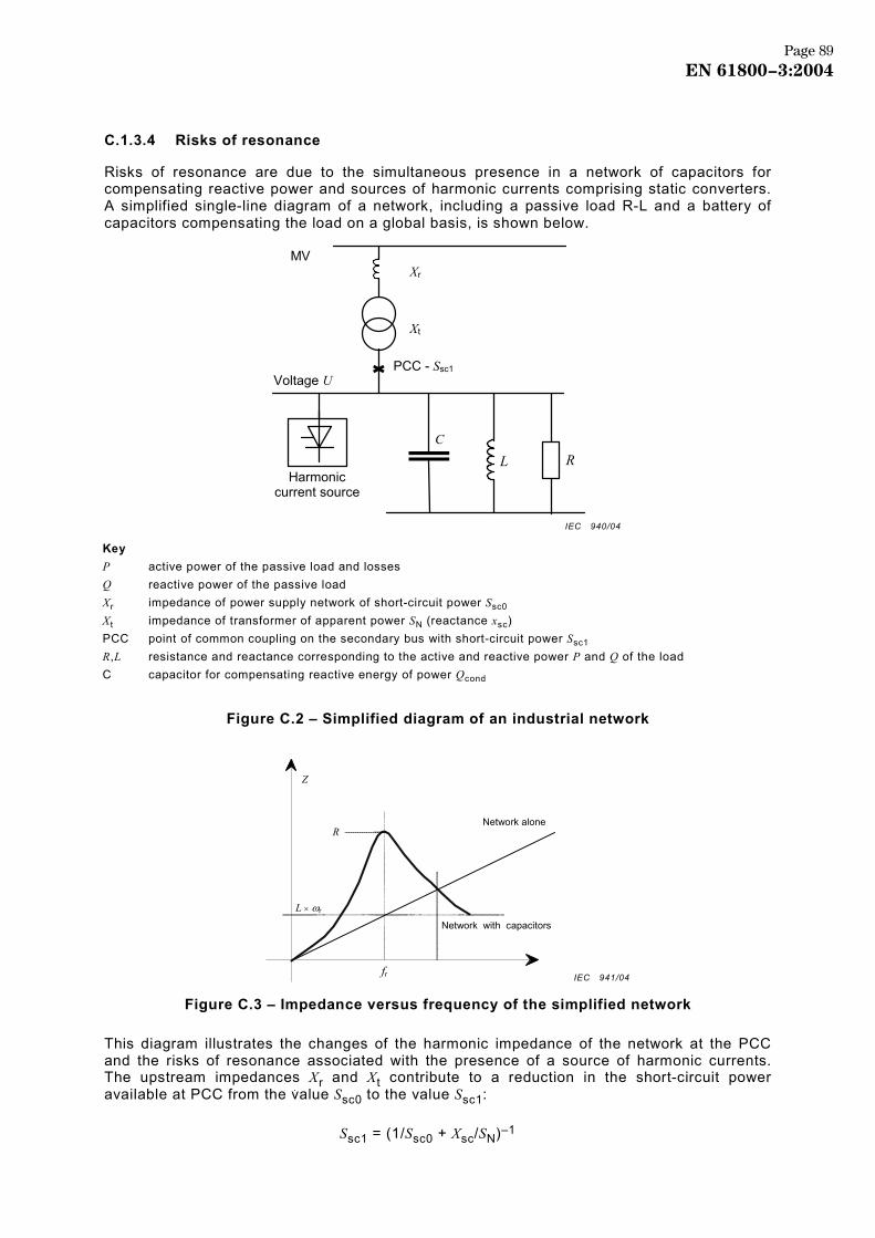
C.1.3.4 Risks of resonance
Risks of resonance are due to the simultaneous presence in a network of capacitors for compensating reactive power and sources of harmonic currents comprising static converters. A simplified single-line diagram of a network, including a passive load R-L and a battery of capacitors compensating the load on a global basis, is shown below.
Xr
Xt
Voltage UPCC - Ssc1
C
Harmoniccurrent source
MV
L R
Key P active power of the passive load and losses Q reactive power of the passive load Xr impedance of power supply network of short-circuit power Ssc0 Xt impedance of transformer of apparent power SN (reactance xsc) PCC point of common coupling on the secondary bus with short-circuit power Ssc1 R,L resistance and reactance corresponding to the active and reactive power P and Q of the load C capacitor for compensating reactive energy of power Qcond
Figure C.2 – Simplified diagram of an industrial network
Z
L × ωr
fr
Network with capacitors
Network alone R
Figure C.3 – Impedance versus frequency of the simplified network
This diagram illustrates the changes of the harmonic impedance of the network at the PCC and the risks of resonance associated with the presence of a source of harmonic currents. The upstream impedances Xr and Xt contribute to a reduction in the short-circuit power available at PCC from the value Ssc0 to the value Ssc1:
Ssc1 = (1/Ssc0 + Xsc/SN)–1
IEC 940/04
IEC 941/04
Page 89EN 61800−3:2004
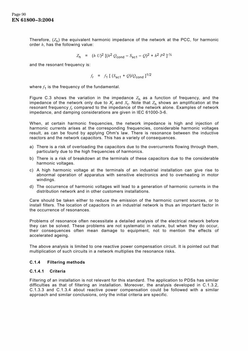
Therefore, (Zh) the equivalent harmonic impedance of the network at the PCC, for harmonic order h, has the following value:
Zh = (h U)2 [(h2 Qcond – Ssc1 – Q)2 + h2 P2 ]-½
and the resonant frequency is:
fr = f1 [ (Ssc1 + Q)/Qcond ]1/2
where f1 is the frequency of the fundamental.
Figure C.3 shows the variation in the impedance Zh as a function of frequency, and the impedance of the network only due to Xr and Xt. Note that Zh shows an amplification at the resonant frequency fr compared to the impedance of the network alone. Examples of network impedance, and damping considerations are given in IEC 61000-3-6.
When, at certain harmonic frequencies, the network impedance is high and injection of harmonic currents arises at the corresponding frequencies, considerable harmonic voltages result, as can be found by applying Ohm's law. There is resonance between the inductive reactors and the network capacitors. This has a variety of consequences.
a) There is a risk of overloading the capacitors due to the overcurrents flowing through them, particularly due to the high frequencies of harmonics.
b) There is a risk of breakdown at the terminals of these capacitors due to the considerable harmonic voltages.
c) A high harmonic voltage at the terminals of an industrial installation can give rise to abnormal operation of apparatus with sensitive electronics and to overheating in motor windings.
d) The occurrence of harmonic voltages will lead to a generation of harmonic currents in the distribution network and in other customers installations.
Care should be taken either to reduce the emission of the harmonic current sources, or to install filters. The location of capacitors in an industrial network is thus an important factor in the occurrence of resonances.
Problems of resonance often necessitate a detailed analysis of the electrical network before they can be solved. These problems are not systematic in nature, but when they do occur, their consequences often mean damage to equipment, not to mention the effects of accelerated ageing.
The above analysis is limited to one reactive power compensation circuit. It is pointed out that multiplication of such circuits in a network multiplies the resonance risks.
C.1.4 Filtering methods
C.1.4.1 Criteria
Filtering of an installation is not relevant for this standard. The application to PDSs has similar difficulties as that of filtering an installation. Moreover, the analysis developed in C.1.3.2, C.1.3.3 and C.1.3.4 about reactive power compensation could be followed with a similar approach and similar conclusions, only the initial criteria are specific.
Page 90EN 61800−3:2004
When an excessively high-voltage distortion level can be expected, filtering should be applied. The voltage distortion level is assessed according to Clauses B.3 and B.4. A particular PDS to be filtered is known with its conventional harmonic emission characteristics, i.e. levels of harmonic current are known. But this characteristic is not sufficient to define a filter.
A filter generally consists of equipment which is connected to the network and which presents a very low impedance at the particular frequencies which have to be filtered. Therefore, the filter absorbs harmonic currents of those particular frequencies. But there is no discrimination between the harmonic current coming from the PDS, and whose preferred path of low impedance is through the filter (instead of the network of higher impedance), and the harmonic current coming from the existing harmonic voltage on the network. The latter current is only limited by the sum of harmonic impedance of the network and impedance of the filter (see Figure C.4). From this discussion, it can be seen that designing a filter is a rather complex affair which requires the knowledge of the three basic parameters:
– current to be filtered, the origin of which is the PDS (responsibility of the manufacturer of the PDS);
– existing harmonic voltage (compatibility levels could be chosen but would generally lead to overrating of the filter);
– harmonic impedance at the PC (responsibility of the operator of the distribution network, who is the user inside the factory in case of IPC, or the operator of the public distribution network in case of PCC).
The design of such filters requires exchange of information between the system supplier and the user.
It is important to note that knowing the harmonic voltage is of no use if the harmonic impedance is unknown. Often, preliminary measurements of voltages and impedance are needed for a correct rating of the filter.
Finally, the risk of multiple resonances is pointed out for similar reasons which have been developed in C.1.3.4.
C.1.4.2 Passive filter
The most traditional filters are resonant circuits (inductance and capacitors in series) or damped circuits by addition of resistors or more complex structures adding poles and zeros to the impedance of the filter.
A filter presents a very low impedance at a particular frequency which is a multiple of the power frequency. A bank of filters using different resonant circuits in parallel provides filtering of several harmonic orders 5, 7, 11, and 13 for example (see Figure C.4). They also may include high pass circuits. They are designed for a fixed power frequency and, in particular when they are only slightly damped, the effectiveness of the filter is dependent upon the stability of the power frequency.
Page 91EN 61800−3:2004
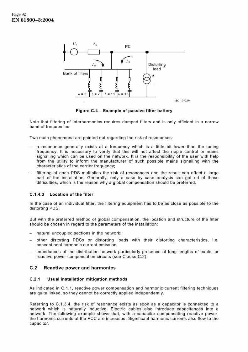
Distortingload
h = 13h = 11h = 7 h = 5
Uh Zh PC
IhlIhn
Bank of filters
Figure C.4 – Example of passive filter battery
Note that filtering of interharmonics requires damped filters and is only efficient in a narrow band of frequencies.
Two main phenomena are pointed out regarding the risk of resonances:
– a resonance generally exists at a frequency which is a little bit lower than the tuning frequency. It is necessary to verify that this will not affect the ripple control or mains signalling which can be used on the network. It is the responsibility of the user with help from the utility to inform the manufacturer of such possible mains signalling with the characteristics of the carrier frequency;
– filtering of each PDS multiplies the risk of resonances and the result can affect a large part of the installation. Generally, only a case by case analysis can get rid of these difficulties, which is the reason why a global compensation should be preferred.
C.1.4.3 Location of the filter
In the case of an individual filter, the filtering equipment has to be as close as possible to the distorting PDS.
But with the preferred method of global compensation, the location and structure of the filter should be chosen in regard to the parameters of the installation:
– natural uncoupled sections in the network; – other distorting PDSs or distorting loads with their distorting characteristics, i.e.
conventional harmonic current emission; – impedances of the distribution network particularly presence of long lengths of cable, or
reactive power compensation circuits (see Clause C.2).
C.2 Reactive power and harmonics
C.2.1 Usual installation mitigation methods
As indicated in C.1.1, reactive power compensation and harmonic current filtering techniques are quite linked, so they cannot be correctly applied independently.
Referring to C.1.3.4, the risk of resonance exists as soon as a capacitor is connected to a network which is naturally inductive. Electric cables also introduce capacitances into a network. The following example shows that, with a capacitor compensating reactive power, the harmonic currents at the PCC are increased. Significant harmonic currents also flow to the capacitor.
IEC 942/04
Page 92EN 61800−3:2004
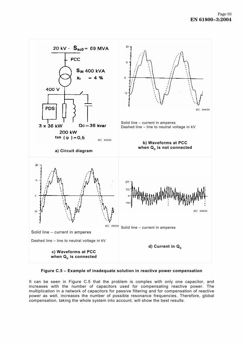
IEC 943/04
a) Circuit diagram
IEC 944/04
Solid line – current in amperes Dashed line – line to neutral voltage in kV
b) Waveforms at PCC when Qc is not connected
IEC 945/04
Solid line – current in amperes
Dashed line – line to neutral voltage in kV
c) Waveforms at PCC when Qc is connected
IEC 946/04
Solid line – current in amperes
d) Current in Qc
Figure C.5 – Example of inadequate solution in reactive power compensation
It can be seen in Figure C.5 that the problem is complex with only one capacitor, and increases with the number of capacitors used for compensating reactive power. The multiplication in a network of capacitors for passive filtering and for compensation of reactive power as well, increases the number of possible resonance frequencies. Therefore, global compensation, taking the whole system into account, will show the best results.
Page 93EN 61800−3:2004
Moreover, proceeding separately to reactive power compensation and to filtering increases the risk of over production of reactive power. Actually, efficient passive filtering also produces a significant amount of reactive power. Therefore, considering both phenomena together gives the opportunity to define a better solution by designing optimum equipment for the whole installation.
C.2.2 Other solutions
C.2.2.1 General
The main drawback of passive filters is often their inability to adapt to network changes and filter component variations (ageing, temperature, etc.). A passive filter is efficient if its impedance at given frequency is very low compared to that of the source. However, in certain cases, compensation becomes difficult if the source (i.e. the network) impedance is low or if the filter frequency characteristics are not accurately tuned to the harmonics generated by the load. But, above all, the most serious problems are series or parallel resonances with the network which can occur.
Consequently, both for the electrical utility and/or the user, other compensation methods can be required to make optimum use of the energy drawn from the network. New solutions, offering better performance, are under consideration and some have already reached the production stage. These solutions are active power filters, and non-polluting PDSs including power factor correction network controls.
C.2.2.2 Active filters
The principle of active filtering consists of connecting between the load and the network power source, a converter consisting of an inverter-type power converter, which can compensate for current or voltage harmonics. When an active filter is connected in parallel and injects a harmonic current to oppose that generated by the load, it is referred to as a parallel or shunt filter. If the active filter is in series with the network, it compensates for the harmonic voltage at the load connection point. The essential advantage of an active filter, compared with a passive filter, is its ability to adapt to network or load changes.
Various filter structures are possible using parallel or series connections. However, it would seem that using active filters in conjunction with passive components could improve performance and extend the potential applications of active filters by reducing ratings, and allowing connections to MV levels. Moreover, there is a slight tendency for the cost of active filters to drop.
C.2.2.3 Non-distorting PDS
New network converter structures represent an alternative to active filters. These single or three-phase structures replace the diode or thyristor line commutated converters. They allow correction of the PDS's power factor both by placing the current drawn from the network in phase with the network voltage and by minimising harmonic currents. The components used in these converters are more expensive since both the turn-on and turn-off switching is controlled. A classical structure for these network converters is the voltage inverter-type power converter, using six transistors or six GTOs. Power drive systems including this type of power factor correction network bridge are named clean or non-distorting PDSs.
Page 94EN 61800−3:2004
C.2.2.4 Application
The costs of such systems are or can be an important part of the costs of the distorting loads that they correct (PDSs or others). This should be understood regarding investment, operation and maintenance as well. Note that operation generates costs with increasing losses and also gains with decreasing reactive power consumption. Costs are balanced with the technical objective which does not allow any alternative to "Ensure EMC" (i.e. compliance with compatibility levels).
Another point is that the compensation can be global, local or combined more easily than with passive solutions because of reduction of resonance risks.
Last but not least, these active solutions increase the number of commutating electronic power devices and are responsible for an increase in high-frequency emissions.
The ideal solution does not exist, and all these elements should be considered. However, the definition of the solution of a particular problem should take into account the particular environment of this problem. The particular environment belongs to a generic class, but is refined by the very knowledge of the industrial conditions in each case.
Page 95EN 61800−3:2004
Annex D (informative)
Considerations on high-frequency emission
D.1 User guidelines
D.1.1 Expected emission of PDSs
D.1.1.1 PDS and its components
In industrial environments, or public networks which do not supply buildings used for domestic purposes, the customers who use PDSs on these networks have a general technical competence and are aware of EMC phenomena.
When selling the components of a PDS, the manufacturer cannot build-in mitigation methods against radio interference, because they are not aware of the EMC boundary conditions of the final installation. Moreover, the user of the components should have a free decision from the economical point of view, to use global or local filtering or screening methods, natural mitigation through distances, or the use of distributed parasitic elements of the existing installation, to achieve electromagnetic compatibility in a case by case manner.
D.1.1.2 Conducted voltage disturbance
The methods and values of quantitative judgement to achieve EMC are well-described in the normative part of this standard. An important item of information for the user of an unfiltered PDS to evaluate possible mitigation methods, is the level of conducted voltage disturbances in the frequency range of 150 kHz up to 30 MHz, which could be expected on the power port of a PDS.
The following results are based on measurements made on several types of PDSs (voltage source type and current source type), located in various countries between 1990 and 1994. For an evaluation of the range of emission levels which can usually be expected, the frequency range was divided into the three usual parts (CISPR 11: 0,15 MHz to 0,50 MHz; 0,50 MHz to 5,0 MHz and 5,0 MHz to 30 MHz), and the maximum level from each PDS in every part was recorded as representative of that section. The measurements were made using peak detectors in most of the cases. A range width of ± 20 dB from the mean value Vdist. was assumed, see Figure D.1, to allow for about 91 % of the variance arising from different load conditions (light load and maximum load), different rated input voltages (230 V, 400 V, 460 V, 690 V) and different rated powers (0,75 kVA to 740 kVA).
According to the physical background of the emission, the average of the peak readings can be arbitrarily approximated by two straight lines with slopes of 20 dB/decade and 40 dB/decade. The two lines cross at the transition frequency ftrans ≈ 2 MHz and, according to reference [7], can be analytically described by
( )µV1kHz10V80log20µV/dBdist ××π
×f
=U
Page 96EN 61800−3:2004
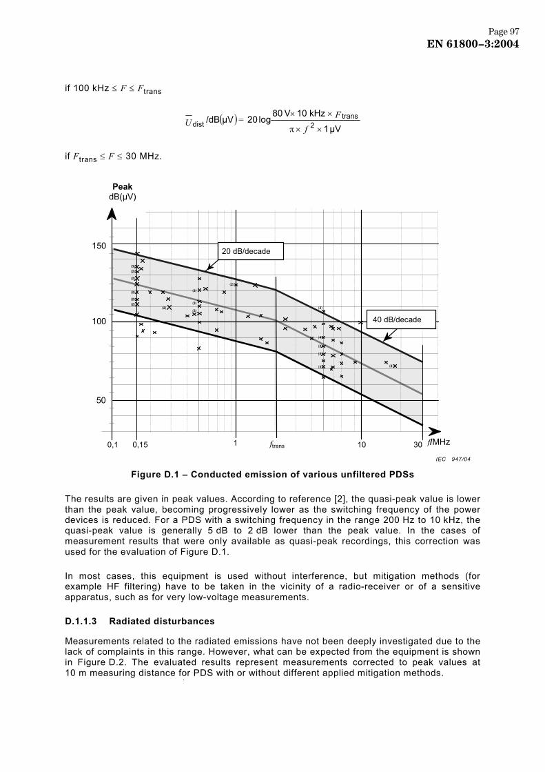
if 100 kHz ≤ F ≤ Ftrans
( )µV1
kHz10V80log20µV/dB
2trans
dist ××π
××
fF=U
if Ftrans ≤ F ≤ 30 MHz.
Peak
dB(µV)
150
100
50
0,1 1 100,15 30 f/MHz
(3)(2)
(2)
(2)
(2)(2)
(2)
(3)
(3)
(2)
(2)
(4)
(2)
(2)
(3) (3)
ftrans
(2)
40 dB/decade
20 dB/decade
Figure D.1 – Conducted emission of various unfiltered PDSs
The results are given in peak values. According to reference [2], the quasi-peak value is lower than the peak value, becoming progressively lower as the switching frequency of the power devices is reduced. For a PDS with a switching frequency in the range 200 Hz to 10 kHz, the quasi-peak value is generally 5 dB to 2 dB lower than the peak value. In the cases of measurement results that were only available as quasi-peak recordings, this correction was used for the evaluation of Figure D.1.
In most cases, this equipment is used without interference, but mitigation methods (for example HF filtering) have to be taken in the vicinity of a radio-receiver or of a sensitive apparatus, such as for very low-voltage measurements.
D.1.1.3 Radiated disturbances
Measurements related to the radiated emissions have not been deeply investigated due to the lack of complaints in this range. However, what can be expected from the equipment is shown in Figure D.2. The evaluated results represent measurements corrected to peak values at 10 m measuring distance for PDS with or without different applied mitigation methods.
IEC 947/04
Page 97EN 61800−3:2004
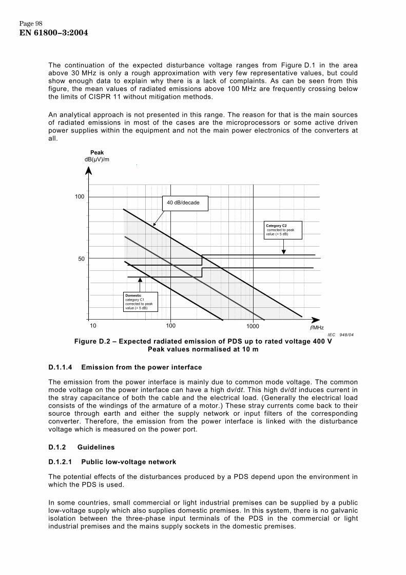
The continuation of the expected disturbance voltage ranges from Figure D.1 in the area above 30 MHz is only a rough approximation with very few representative values, but could show enough data to explain why there is a lack of complaints. As can be seen from this figure, the mean values of radiated emissions above 100 MHz are frequently crossing below the limits of CISPR 11 without mitigation methods.
An analytical approach is not presented in this range. The reason for that is the main sources of radiated emissions in most of the cases are the microprocessors or some active driven power supplies within the equipment and not the main power electronics of the converters at all.
PeakdB(µV)/m
100
50
10 100 1000 f/MHz
Category C2 corrected to peakvalue (+ 5 dB)
40 dB/decade
Domesticcategory C1corrected to peakvalue (+ 5 dB)
Figure D.2 – Expected radiated emission of PDS up to rated voltage 400 V
Peak values normalised at 10 m
D.1.1.4 Emission from the power interface
The emission from the power interface is mainly due to common mode voltage. The common mode voltage on the power interface can have a high dv/dt. This high dv/dt induces current in the stray capacitance of both the cable and the electrical load. (Generally the electrical load consists of the windings of the armature of a motor.) These stray currents come back to their source through earth and either the supply network or input filters of the corresponding converter. Therefore, the emission from the power interface is linked with the disturbance voltage which is measured on the power port.
D.1.2 Guidelines
D.1.2.1 Public low-voltage network
The potential effects of the disturbances produced by a PDS depend upon the environment in which the PDS is used.
In some countries, small commercial or light industrial premises can be supplied by a public low-voltage supply which also supplies domestic premises. In this system, there is no galvanic isolation between the three-phase input terminals of the PDS in the commercial or light industrial premises and the mains supply sockets in the domestic premises.
IEC 948/04
Page 98EN 61800−3:2004
Where an unsuppressed PDS is directly connected to a public low-voltage supply which supplies domestic premises, there is a significant risk of disturbance to radio and television reception. In this environment, it is strongly recommended that the mains input of the PDS be filtered. Therefore, the user should select a PDS which complies with the appropriate limits given in 6.4 of this standard.
D.1.2.2 Second environment
In an industrial environment, not on a public low-voltage supply, the common practice for many years has been to use unfiltered PDSs. In general, these have worked correctly and have not disturbed other equipment. This has been shown by a general lack of complaints about radio interference in industry. Therefore, they are compatible.
If problems do occur, they are likely to be due to the conducted disturbances from the BDM/CDM. These disturbances propagate along the supply and motor cables and can be coupled into other equipment by conduction, inductive or capacitive coupling, or radiation.
There can be problems if an unfiltered PDS is used in close proximity to particularly sensitive equipment. However, a PDS may not be the only source of disturbance and the sensitive equipment is usually of lower power rating than the PDS. Therefore, improving the immunity of the sensitive equipment can be a more economic solution than filtering the emissions from the PDS.
Problems are usually prevented by following normal installation guidelines, involving segregation of signal and power cables. If these are insufficient, either the immunity of the victim should be increased or the emissions from the PDS should be reduced, depending on which is the most economic solution.
The use of a commercially available EMC filter on the power interface between the BDM/CDM and the motor can lead to problems. It is likely that the capacitors in this filter would be damaged by the fast switching edges present on the BDM/CDM end of this interface.
If a shielded or armoured cable is used for the connection between the BDM/CDM and the motor without the BDM/CDM input being filtered, the coupling from the motor cable will decrease, but the conducted disturbances in the mains supply will increase, due to the capacitance of the armoured cable. Therefore, if a shielded or armoured cable between BDM/CDM and motor is being used to solve an EMC problem, a filter should be connected to the mains input of the BDM/CDM. However, minimising the length of the motor cable will generally assist in reduction of radiated emission of this cable.
Since filtering would cause safety problems in systems which are isolated from earth, the only solution in this case is to ensure that other equipment has sufficient immunity for this environment. In the case of systems in which one live line is connected to earth (known in some countries as “corner grounded” systems), the Y-class (line-to-earth) capacitors should be rated for the full line-to-line voltage.
D.1.2.3 Categories C1 and C3
The manufacturer should provide the information necessary for the user to select the correct emission category and to install the equipment correctly. This information should include clear instructions on the installation of any filters supplied as loose items. If special cables are required, this should also be stated.
Page 99EN 61800−3:2004
Cabinet builders often use insulation withstand tests to check the quality of their wiring. However, an EMC filter is usually less able to withstand this test than the power converter. Therefore, the manufacturer should provide clear instructions on this subject to the user.
If the PDS is unsuppressed or of a high emission category, the manufacturer should indicate this clearly in the user documentation. In this case, according to 6.4.1.1 and 6.4.1.3, the manufacturer shall provide a warning that the PDS is not to be used in a public low-voltage network which supplies domestic premises.
If the PDS generates commutation notches on the input, this should be indicated in the user information.
In case of problems, the manufacturer should offer (at the cost of the user), the solution necessary to make the PDS comply with a lower emission category.
D.1.2.4 Categories C2 and C4
In this case, the user has the technical competence to apply a correct EMC concept for the installation. The manufacturer should provide information about the emission category of the PDS.
The user will be able to select the correct combination of emission category and mitigation measures to provide the most economic solution for the installation.
D.2 Safety and RFI-filtering in power supply systems
D.2.1 Safety and leakage currents
The RFI-filtering sufficient to meet the emission limits is well-known in the state of the art. It is important to consider that the capacitance values and therefore the energy content and finally the effectiveness of Y-type capacitors used for the filters is limited by the normative requirements of safety standards, such as IEC 60065 in the case of plug-in apparatus. If the leakage current through this RFI-filtering capacitance to earth is too high, the effectiveness of differential protection (earth fault protection) within these supply systems can be compromised.
Safety requirements related to leakage current, including requirements for warnings, are given in IEC 61800-5-1.
D.2.2 Safety and RFI-filtering in power supply systems isolated from earth
In complex processes like rolling mills, bar mills or paper mills as well as centrifugal and auxiliary equipment in the sugar industry, crane equipment and chemical industry, it is useful and state of the art to have a distributed isolated power supply system. Even if, for example, the motors are installed outside the building and are exposed to high humidity, it may be necessary to continue the process in spite of one short circuit to earth. This short circuit is detected via an "earth fault monitoring system" and allows the whole process to be safely run until the next service interval.
Page 100EN 61800−3:2004
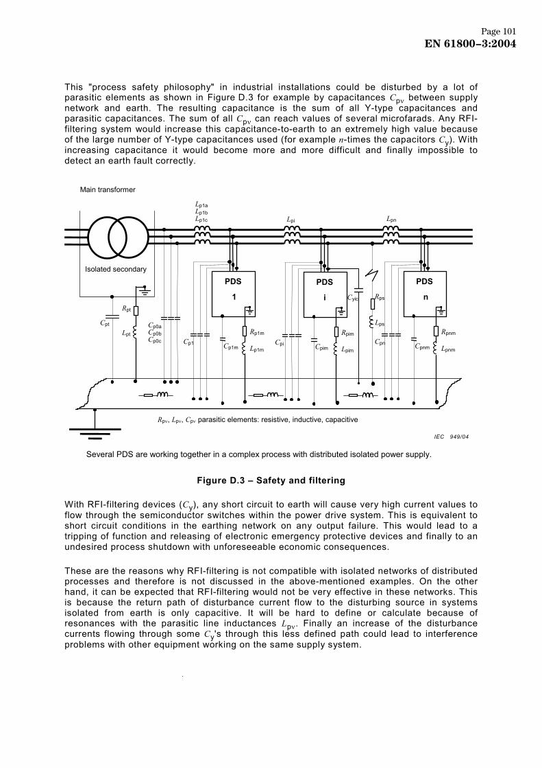
This "process safety philosophy" in industrial installations could be disturbed by a lot of parasitic elements as shown in Figure D.3 for example by capacitances Cpν between supply network and earth. The resulting capacitance is the sum of all Y-type capacitances and parasitic capacitances. The sum of all Cpν can reach values of several microfarads. Any RFI-filtering system would increase this capacitance-to-earth to an extremely high value because of the large number of Y-type capacitances used (for example n-times the capacitors Cy). With increasing capacitance it would become more and more difficult and finally impossible to detect an earth fault correctly.
Several PDS are working together in a complex process with distributed isolated power supply.
Rpν, Lpν, Cpν parasitic elements: resistive, inductive, capacitive
Main transformer
Isolated secondary
Lp1aLp1bLp1c
Cpt
Rpt
LptCp0aCp0bCp0c
PDS
1
Cp1 Cp1m
Rp1m
Lp1m
Lpi
PDS
i
Cpi Cpim
Rpim
Lpim
Lpn
PDS
n
Cpn Cpnm
Rpnm
Lpnm
Rps
Lps
Cyic
Figure D.3 – Safety and filtering
With RFI-filtering devices (Cy), any short circuit to earth will cause very high current values to flow through the semiconductor switches within the power drive system. This is equivalent to short circuit conditions in the earthing network on any output failure. This would lead to a tripping of function and releasing of electronic emergency protective devices and finally to an undesired process shutdown with unforeseeable economic consequences.
These are the reasons why RFI-filtering is not compatible with isolated networks of distributed processes and therefore is not discussed in the above-mentioned examples. On the other hand, it can be expected that RFI-filtering would not be very effective in these networks. This is because the return path of disturbance current flow to the disturbing source in systems isolated from earth is only capacitive. It will be hard to define or calculate because of resonances with the parasitic line inductances Lpν. Finally an increase of the disturbance currents flowing through some Cy's through this less defined path could lead to interference problems with other equipment working on the same supply system.
IEC 949/04
Page 101EN 61800−3:2004
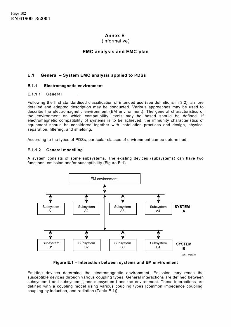
Annex E (informative)
EMC analysis and EMC plan
E.1 General – System EMC analysis applied to PDSs
E.1.1 Electromagnetic environment
E.1.1.1 General
Following the first standardised classification of intended use (see definitions in 3.2), a more detailed and adapted description may be conducted. Various approaches may be used to describe the electromagnetic environment (EM environment). The general characteristics of the environment on which compatibility levels may be based should be defined. If electromagnetic compatibility of systems is to be achieved, the immunity characteristics of equipment should be considered together with installation practices and design, physical separation, filtering, and shielding.
According to the types of PDSs, particular classes of environment can be determined.
E.1.1.2 General modelling
A system consists of some subsystems. The existing devices (subsystems) can have two functions: emission and/or susceptibility (Figure E.1).
SYSTEMA
EM environment
SYSTEMB
SubsystemA4
SubsystemA3
SubsystemA2
SubsystemA1
SubsystemB4
SubsystemB3
SubsystemB2
SubsystemB1
Figure E.1 – Interaction between systems and EM environment
Emitting devices determine the electromagnetic environment. Emission may reach the susceptible devices through various coupling types. General interactions are defined between subsystem i and subsystem j, and subsystem i and the environment. These interactions are defined with a coupling model using various coupling types [common impedance coupling, coupling by induction, and radiation (Table E.1)].
IEC 950/04
Page 102EN 61800−3:2004
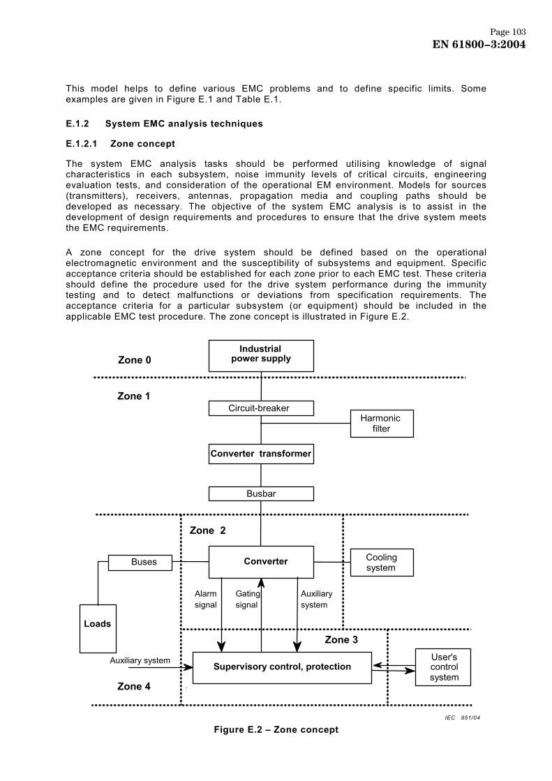
This model helps to define various EMC problems and to define specific limits. Some examples are given in Figure E.1 and Table E.1.
E.1.2 System EMC analysis techniques
E.1.2.1 Zone concept
The system EMC analysis tasks should be performed utilising knowledge of signal characteristics in each subsystem, noise immunity levels of critical circuits, engineering evaluation tests, and consideration of the operational EM environment. Models for sources (transmitters), receivers, antennas, propagation media and coupling paths should be developed as necessary. The objective of the system EMC analysis is to assist in the development of design requirements and procedures to ensure that the drive system meets the EMC requirements.
A zone concept for the drive system should be defined based on the operational electromagnetic environment and the susceptibility of subsystems and equipment. Specific acceptance criteria should be established for each zone prior to each EMC test. These criteria should define the procedure used for the drive system performance during the immunity testing and to detect malfunctions or deviations from specification requirements. The acceptance criteria for a particular subsystem (or equipment) should be included in the applicable EMC test procedure. The zone concept is illustrated in Figure E.2.
Alarmsignal
Gatingsignal
Auxiliarysystem
Industrialpower supply
Circuit-breaker
Converter transformer
Busbar
Converter
Supervisory control, protection
Zone 0
Zone 1
Harmonicfilter
Coolingsystem
User'scontrolsystem
Zone 3
Auxiliary system
Loads
Zone 4
Buses
Zone 2
Figure E.2 – Zone concept
IEC 951/04
Page 103EN 61800−3:2004
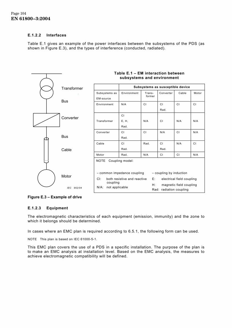
E.1.2.2 Interfaces
Table E.1 gives an example of the power interfaces between the subsystems of the PDS (as shown in Figure E.3), and the types of interference (conducted, radiated).
Figure E.3 – Example of drive
Transformer
Bus
Converter
Cable
Motor
Bus
Table E.1 – EM interaction between
subsystems and environment
Subsystems as susceptible device
Subsystems as
EM-source
Environment Trans-former
Converter Cable Motor
Environment N/A CI CI
Rad.
CI CI
Transformer
CI
E, H,
Rad.
N/A
CI
N/A
N/A
Converter CI
Rad.
CI N/A CI N/A
Cable CI
Rad.
Rad. CI
Rad.
N/A CI
Motor Rad. N/A CI CI N/A
NOTE Coupling model:
– common impedance coupling
CI: both resistive and reactive coupling
N/A: not applicable
– coupling by induction
E: electrical field coupling
H: magnetic field coupling Rad: radiation coupling
E.1.2.3 Equipment
The electromagnetic characteristics of each equipment (emission, immunity) and the zone to which it belongs should be determined.
In cases where an EMC plan is required according to 6.5.1, the following form can be used.
NOTE This plan is based on IEC 61000-5-1.
This EMC plan covers the use of a PDS in a specific installation. The purpose of the plan is to make an EMC analysis at installation level. Based on the EMC analysis, the measures to achieve electromagnetic compatibility will be defined.
IEC 952/04
Page 104EN 61800−3:2004
E.2 Example of EMC plan for general applications
E.2.1 Project data and description
According to 6.5.1, the EMC plan reflects the agreement and the exchange of technical data between the user and the manufacturer. It should define the responsibilities of the manufacturer of the PDS, the installer and the user. The EMC plan is established jointly by all three parties. Any question which is not relevant to the particular application may be omitted.
The EMC plan is divided into two parts:
– E.2 defines the items which should normally be agreed; – E.3 defines additional items that may be necessary in certain applications. NOTE Use marking N/A if the requirement is not applicable. Provide explanation in such a case.
The example proposed below contains questions, the answers to which can constitute an EMC plan.
Name of manufacturer/supplier Name of end user Order No. ................................................. ................................. Date
Type of facility (e.g. chemical factory, paper machine) Application (e.g. pump. fan, conveyor) ..... EMC responsible person(s) ......................
E.2.2 Electromagnetic environment analysis
E.2.2.1 Facility data
Installation location
Description of the neighbourhood (next to the second environment in which the PDS is installed) First environment Second environment The distance from the building/room of PDS to first environment: ................. metres The distance from the building/room of PDS to the other premises in the second environment: ........................... metres
Building and room construction
Type (wood, brick, concrete, steel, aluminium, etc.) .......................... Reinforcement (steel, etc.) Yes .................... No ..................... Dedicated room for system Yes .................... No......................
Room layout Sketch room layout as close to scale as possible. Shows all major equipment: windows, doors, etc.
Page 105EN 61800−3:2004

E.2.2.2 Power and earthing data
Power distribution
Power distribution system for PDS: Identification of the point of coupling (identification code for distribution panel, switchgear or transformer) ........ Type of distribution system (example TN-C, TN-S; TT, IT) The type of power supply for PDS: Wye ...... Delta .... Number of phases ... Number of wires ..... Earth bus: how and where bonded ? ................
Wiring diagram Draw a single-line diagram of site power distribution system from the main supply transformer to the PDS. Show all transformers, distribution panels, etc. Also indicate nominal voltage, power rating, cable routing and method, number of conductors and approximate length of cables/busbars involved.
E.2.2.3 EMC data
PDS earthing
PDS earth reference? ...... Single point ........ Meshed ......... Provide a schematic of equipotential bonding.
PDS shielding
Are shielded cabinets for CDM/BDM used? Yes....... No ........ Describe:
Are shielded cables used? Yes....... No ........ Describe:
Other measures used (e.g. container)? Yes....... No ........ Describe (consider also motors and cables):
RFI sensitive equipment in facility
Any equipment in the building or near installation location sensitive to RF disturbances? Yes ............................... No Describe: (e.g. process control and measurement, data buses, computers, etc.)
Approximate distance from PDS/cabling of PDS: ...................................... metres Most likely coupling path for disturbance: Conducted.......... Radiated ......
RFI sensitive equipment outside facility
Any broadcast or communications receiver antennas visible or near facility? Yes ............................... No Describe (e.g. radar, radio/TV broadcast, amateur, microwave or other): Frequency .......... Distances from the antenna ............................. metres
Citizen band (CB), walkie-talkies, wireless communication, remote control or clock synchronisation system used on facility? Yes ............................... No Describe:
Page 106EN 61800−3:2004
E.2.3 EMC analysis
E.2.3.1 Identify the most sensitive equipment or systems:
Analyse electromagnetic environment constraints to installation.
E.2.3.2 Identify the most likely disturbing parts of PDS:
Analyse electromagnetic environment constraints to installation.
E.2.3.3 Are there risks of malfunction of items listed in a), due to disturbances from the PDS?
Yes ............................... No Describe:
E.2.4 Establishment of installation rules
E.2.4.1 Earthing
Note the recommendations given by the manufacturer of PDS, when determining the installation rules. To ensure the EMC effectiveness of the earthing, assess the items below:
– earthing system of PDS (single point/meshed); – equipotential bonding
• interconnection of exposed conductive parts,
• interconnection of metal structures of PDS to the earthing system; – HF quality of connections
• metal-to-metal bonding by fasteners,
• removal of paint or any other insulating material where necessary; – describe (EMC solutions)
E.2.4.2 Cables and wiring
E.2.4.2.1 Cable selection
Note the recommendations given by the manufacturer of PDS, when determining the installation rules. To ensure the EMC effectiveness of cables, assess the items below:
– the signal type (e.g. digital data, PWM to a motor, etc.); – unused conductors; – type of cable and type of shielding (if any); – describe (EMC solutions)
E.2.4.2.2 Routing
Note the recommendations given by the manufacturer of PDS, when determining the installation rules. To ensure the EMC effectiveness of cabling, assess the items below:
– separation of high-power and low power, or signal cables; – minimisation of parallel length; – segregation distances;
– cable intersection at 90°; – use of conduits and cable trays as parallel-earthed conductor;
Page 107EN 61800−3:2004
– cable positioning in cable trays; – earthing of cable trays; – describe (EMC solutions).
E.2.4.3 Shielding of PDS cabinet
Note the recommendations given by the manufacturer of PDS, when determining the installation rules. To ensure the EMC effectiveness of enclosures, assess the items below:
– continuity of metallic enclosure; – dimension of slots and openings; – cable entry through the earth reference plane;
– connection of cable shields to earth reference plane (360° preferred); – describe (EMC solutions).
E.2.4.4 Dedicated transformer
Note the recommendations given by the manufacturer of PDS, when determining the installation rules. To ensure EMC effectiveness, consider the use of the following:
– dedicated isolation transformer; – transformer with electrostatic shield; – describe (size, location).
E.2.4.5 Filtering
Note the recommendations given by the manufacturer of PDS, when determining the installation rules. To ensure EMC effectiveness, consider the use of the following:
– centralised or distributed RFI-filter-configurations; – signal line filtering; – filtering power interface if appropriate; – describe (EMC solutions)
E.2.4.6 Additional mitigation techniques
Note the recommendations given by the manufacturer of PDS, when determining the installation rules. Are other mitigation techniques necessary? Yes No
Consider the use of the following:
– electrical separation of circuits; – optical fibres; – galvanic isolation for data lines (example optocouplers, transformers); – extra protection for sensitive devices; – describe (EMC solutions)
Page 108EN 61800−3:2004
E.2.5 Formal result and maintenance
Check that the installation is built according to the defined installation rules.
Do all details follow the defined installation rules? Yes No
Describe any action to correct failings.
Define instructions for maintaining EMC characteristics of the installation (e.g. measures against corrosion, dust which might weaken the contact between the door and the frame, loosening of connections, etc.).
Signature(s) by person(s) responsible for EMC:
Date
Signature(s)
E.3 Example of supplement to EMC plan for particular application
E.3.1 Electromagnetic environment complementary analysis
E.3.1.1 Power distribution from utility substation to facility main supply transformer
The questions in E.3 are related to factors external to the PDS which can be relevant to the EMC performance in a more complex application.
Electrical utility service supplier:
Approximate distance from the nearest utility substation (if known): Utility service distribution from the substation: overhead lines buried combination describe
Facility main supply transformer characteristic: kVA
input (primary): volts number of phases type of connection: Delta Wye other, describe
Output to internal distribution (secondary)
volts number of wires number of phases Type of connection: Delta Wye Is the transformer earthed? (describe how and where)
Building earthing electrode consisting of
Earth rod Multiple rods Earth grid Earth plate Buried conduit Water pipe Building steel If other, describe
Page 109EN 61800−3:2004
Draw wiring diagram
Draw a single-line diagram of site power distribution system from the utility substation to main supply transformer. Show all transformers, distribution panels, etc.
Earth electrode impedance in ohms (if known)
E.3.1.2 Power distribution from facility main supply transformer to local distribution panel/switch gear/transformer for PDS
The questions in E.3 are related to factors external to the PDS which can be relevant to the EMC performance in a more complex application.
Wiring diagram
Draw a single-line diagram of facility power distribution system from the main supply transformer to the local distribution panel/switchgear/transformer.
Local power distribution panel/switchgear/transformer
Panel/switchgear/transformer identification
Panel construction: how and where bonded
Type of power supply for panel/switchgear/transformer
Wye Delta number of phases
number of wires wire size (phase/neutral/PE): Cu Al
Neutral bus: how and where bonded
Earth bus: how and where bonded
Individual insulated PE wire from PDS or part of PDS
Yes No
Describe
E.3.2 EMC analysis
E.3.2.1 Frequency plan
RFI survey needed
Yes No
Explain
If yes, issuing a frequency plan/table might clarify the situation. An example is given below in Table E.2.
Page 110EN 61800−3:2004
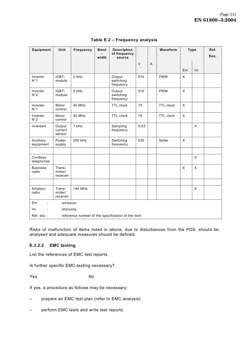
Table E.2 – Frequency analysis
Equipment Unit Frequency Band-
width
Description of frequency
source
Waveform Type Ref.
Doc.
V A
Em
Im
Inverter N°1
IGBT-module
5 kHz Output switching frequency
510 PWM X
Inverter N°2
IGBT-module
5 kHz Output switching frequency
510 PWM X
Inverter N°1
Motor control
40 MHz TTL clock 15 TTL clock X
Inverter N°2
Motor control
40 MHz TTL clock 15 TTL clock X
Inverters Output current sensor
1 kHz Sampling frequency
0,03 X
Auxiliary equipment
Power supply
200 kHz Switching frequency
230 Spike X
Cordless telephones
X
Business radio
Trans-mitter/ receiver
X X
Amateur radio
Trans-mitter/ receiver
144 MHz X
Em : emission
Im : immunity
Ref. doc : reference number of the specification of the item
Risks of malfunction of items listed in above, due to disturbances from the PDS, should be analysed and adequate measures should be defined.
E.3.2.2 EMC testing
List the references of EMC test reports.
Is further specific EMC-testing necessary?
Yes No
If yes, a procedure as follows may be necessary:
– prepare an EMC test plan (refer to EMC analysis)
– perform EMC tests and write test reports.
Page 111EN 61800−3:2004

Are the test results acceptable?
Yes No
Describe any action to correct failings:
Page 112EN 61800−3:2004
Annex ZA (normative)
Normative references to international publications
with their corresponding European publications
The following referenced documents are indispensable for the application of this document. For dated references, only the edition cited applies. For undated references, the latest edition of the referenced document (including any amendments) applies.
NOTE Where an international publication has been modified by common modifications, indicated by (mod), the relevant EN/HD applies.
Publication Year Title EN/HD Year
IEC 60050-131 2002 International Electrotechnical Vocabulary Part 131: Circuit theory
- -
IEC 60050-151 2001 Part 151: Electrical and magnetic devices
- -
IEC 60050-161 1990 Chapter 161: Electromagnetic compatibility
- -
IEC 60146-1-1 1991 Semiconductor convertors - General requirements and line commutated convertors Part 1-1: Specifications of basic requirements
EN 60146-1-1 1993
IEC 60364-1 2001 Electrical installations of buildings Part 1: Fundamental principles, assessment of general characteristics, definitions
- -
IEC 60664-1 1992 Insulation coordination for equipment within low-voltage systems Part 1: Principles, requirements and tests
EN 60664-1 1) 2003
IEC/TR 61000-1-1 – 2) Electromagnetic compatibility (EMC) Part 1: General - Section 1: Application and interpretation of fundamental definitions and terms
- -
IEC/TR 61000-2-1 1990 Part 2: Environment - Section 1: Description of the environment - Electromagnetic environment for low-frequency conducted disturbances and signalling in public power supply systems
- -
1) EN 60664-1 includes A1:2000 + A2:2002 to IEC 60664-1.
2) Undated reference.
Page 113EN 61800−3:2004
Publication Year Title EN/HD Year
IEC 61000-2-2 2002 Part 2-2: Environment - Compatibility levels for low-frequency conducted disturbances and signalling in public low-voltage power supply systems
EN 61000-2-2 2002
IEC 61000-2-4 2002 Part 2-4: Environment - Compatibility levels in industrial plants for low-frequency conducted disturbances
EN 61000-2-4 2002
IEC 61000-2-6 1995 Part 2-6: Environment - Assessment of the emission levels in the power supply of industrial plants as regards low-frequency conducted disturbances
- -
IEC 61000-3-2 (mod)
2000 Part 3-2: Limits - Limits for harmonic current emissions (equipment input current up to and including 16 A per phase)
EN 61000-3-2 2000
IEC 61000-3-3 1994 Part 3-3: Limits - Limitation of voltage changes, voltage fluctuations and flicker in public low-voltage supply systems, for equipment with rated current ≤16 A per phase and not subject to conditional connection
EN 61000-3-3 + corr. July
1995 1997
IEC/TS 61000-3-4 1998 Electromagnetic compatibility (EMC) Part 3-4: Limits - Limitation of emission of harmonic currents in low-voltage power supply systems for equipment with rated current greater than 16 A
- -
IEC 61000-3-7 1996 Electrical apparatus for the detection and measurement of combustible gases, toxic gases or oxygen - Requirements and tests for apparatus using software and/or digital technologies
- -
IEC 61000-3-11 2000 Part 3-11: Limits - Limitation of voltage changes, voltage fluctuations and flicker in public low-voltage supply systems - Equipment with rated current ≤ 75 A and subject to conditional connection
EN 61000-3-11 2000
IEC 61000-4-2 – 2) Part 4-2: Testing and measurement techniques - Electrostatic discharge immunity test
EN 61000-4-2 1995 3)
IEC 61000-4-3 2002 Part 4-3: Testing and measurement techniques - Radiated, radio-frequency, electromagnetic field immunity test
EN 61000-4-3 2002
3) Valid edition at date of issue.
Page 114EN 61800−3:2004
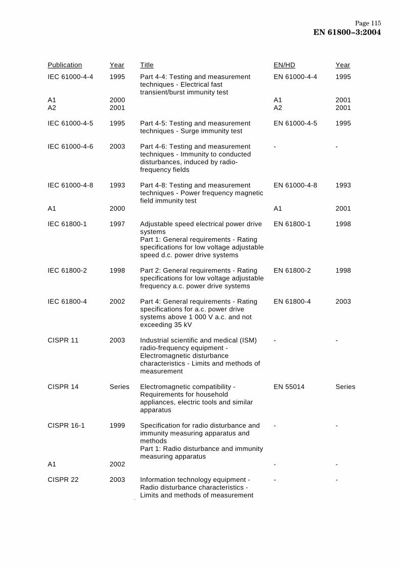
Publication Year Title EN/HD Year
IEC 61000-4-4 1995 Part 4-4: Testing and measurement techniques - Electrical fast transient/burst immunity test
EN 61000-4-4 1995
A1 2000 A1 2001 A2 2001
A2 2001
IEC 61000-4-5 1995 Part 4-5: Testing and measurement techniques - Surge immunity test
EN 61000-4-5 1995
IEC 61000-4-6 2003 Part 4-6: Testing and measurement techniques - Immunity to conducted disturbances, induced by radio-frequency fields
- -
IEC 61000-4-8 1993 Part 4-8: Testing and measurement techniques - Power frequency magnetic field immunity test
EN 61000-4-8 1993
A1 2000
A1 2001
IEC 61800-1 1997 Adjustable speed electrical power drive systems Part 1: General requirements - Rating specifications for low voltage adjustable speed d.c. power drive systems
EN 61800-1 1998
IEC 61800-2 1998 Part 2: General requirements - Rating specifications for low voltage adjustable frequency a.c. power drive systems
EN 61800-2 1998
IEC 61800-4 2002 Part 4: General requirements - Rating specifications for a.c. power drive systems above 1 000 V a.c. and not exceeding 35 kV
EN 61800-4 2003
CISPR 11 2003 Industrial scientific and medical (ISM) radio-frequency equipment - Electromagnetic disturbance characteristics - Limits and methods of measurement
- -
CISPR 14 Series Electromagnetic compatibility - Requirements for household appliances, electric tools and similar apparatus
EN 55014 Series
CISPR 16-1 1999 Specification for radio disturbance and immunity measuring apparatus and methods Part 1: Radio disturbance and immunity measuring apparatus
- -
A1 2002
- -
CISPR 22 2003 Information technology equipment - Radio disturbance characteristics - Limits and methods of measurement
- -
Page 115EN 61800−3:2004
Annex ZZ (informative)
Coverage of Essential Requirements of EC Directives
This European Standard has been prepared under a mandate given to CENELEC by the European Commission and the European Free Trade Association and within its scope the standard covers all relevant essential requirements as given in Article 4 of the EC Directive 89/336/EEC.
Compliance with this standard provides one means of conformity with the specified essential requirements of the Directive[s] concerned.
WARNING: Other requirements and other EC Directives may be applicable to the products falling within the scope of this standard.
__________
Page 116EN 61800−3:2004
Bibliography
[1] ENEL (Italian Electricity Supply Industry) Specification GLI (EMC) 07, Appendix A
[2] T. Williams: "EMC for Product Designers" – Butterworth-Heinemann Ltd, Oxford, 1992
[3] IEC 61000-4-3:1995, Electromagnetic compatibility (EMC) – Part 4: Testing and measurement techniques – Section 3: Radiated, radio-frequency, electromagnetic field. immunity test – Annex A
[4] Post Verfügung. Amtsbl Vfg 1045 – December 1984 Anlage 1 – § 2, Nr 4
"... for installations, or for components which are parts of an installation, no mark of built-in radio-interference suppression is required, but that the customer attention shall be drawn to the aspect, that for the final installation mitigation measures could be necessary...".
[5] Post Verfügung Amtsbl Vfg 1046-1984 Anlage 1, § 6 & § 7
[6] Regulations of documents mentioned in the references [4] and [5] are harmonized with the electrotechnical standard VDE 0875
[7] W. Graupner; Rolle, S.: "Funkstörspannungen leistungselektronischer Antriebe" Symposium der Gesellschaft für Mikroelektronik GME des VDI, Frankfurt 1993
China "Provisional Regulation for Harmonics in Electricity Distribution Systems." SD 126-84
Germany "Grundsätze für die Beurteilung von Netzrückwirkungen." VDEW 1992
Switzerland "Limitation des Perturbations Electriques dans les Réseaux Publics de distribution. ASE 3600-1-1987 et ASE 3600-1987/SNV4 3600-1 et -2
United-Kingdom "Planning levels for harmonic voltage distortion and the connection of non-linear equipment to transmission systems and distribution networks in the United Kingdom " G5/4 February 2001 from Electricity Association
USA "IEEE Recommended Practices and Requirements for Harmonic Control in Electric Power Systems." IEEE 519-1992
IEC 60038:1983, IEC standard voltages
IEC 60050(101):1998, International Electrotechnical Vocabulary (IEV) – Part 101: Mathematics
IEC 60050(551):1998, International Electrotechnical Vocabulary (IEV) – Chapter 551: Power electronics
IEC 60050-551-20:2001, International Electrotechnical Vocabulary (IEV) – Part 551-20: Power electronics – Harmonic analysis
Page 117EN 61800−3:2004
IEC 60146-1-2:1991, Semiconductor convertors – General requirements and line commutated convertors – Part 1-2: Application guide
IEC 60146-1-3:1991, Semiconductor convertors – General requirements and line commutated convertors – Part 1-3: Transformers and reactors
IEC 60146-2:1999, Semiconductor convertors – General requirements and line commutated convertors – Part 2: Self-commutated semiconductor converters including direct d.c. converters
IEC 61000-2-3:1992, Electromagnetic compatibility (EMC) – Part 2: Environment – Section 3: Description of the environment – Radiated and non-network-frequency-related conducted phenomena
IEC 61000-2-5:1995, Electromagnetic compatibility (EMC) – Part 2: Environment – Section 5: Classification of electromagnetic environments – Basic EMC publication
IEC 61000-2-8:2002, Electromagnetic compatibility (EMC) – Part 2-8: Environment – Voltage dips and short interruptions on public electric power supply systems with statistical measurement results
IEC 61000-2-12:2003, Electromagnetic compatibility (EMC) – Part 2-12: Environment –Compatibility levels for low-frequency conducted disturbances and signalling in public medium-voltage power supply systems
IEC 61000-3-5:1994, Electromagnetic compatibility (EMC) – Part 3: Limits – Section 5: Limitation of voltage fluctuations and flicker in low-voltage power supply systems for equipment with rated current greater than 16 A
IEC 61000-3-6:1996, Electromagnetic compatibility (EMC) – Part 3: Limits – Section 6: Assessment of emission limits for distorting loads in MV and HV power systems – Basic EMC publication
IEC 61000-3-12, Electromagnetic compatibility (EMC) – Part 3-12: Limits for harmonic currents produced by equipment connected to public low-voltage systems with input current ≤75 A per phase and subject to restricted connection2
IEC 61000-4-1:2000, Electromagnetic compatibility (EMC) – Part 4-1: Testing and measure-ment techniques – Overview of IEC 61000-4 series
IEC 61000-4-7:2002, Electromagnetic compatibility (EMC) – Part 4: Testing and measurement techniques – Section 7: General guide on harmonics and interharmonics measurements and instrumentation, for power supply systems and equipment connected thereto
IEC 61000-4-9:1993, Electromagnetic compatibility (EMC) – Part 4: Testing and measurement techniques – Section 9: Pulse magnetic field immunity test – Basic EMC publication
IEC 61000-4-10:1993, Electromagnetic compatibility (EMC) – Part 4: Testing and measure-ment techniques – Section 10: Damped oscillatory magnetic field immunity tes –. Basic EMC publication
——————— 2 To be published.
Page 118EN 61800−3:2004
IEC 61000-5-1:1996, Electromagnetic compatibility (EMC) – Part 5: Installation and mitigation guidelines – Section 1: General consideration – Basic EMC publication
IEC 61000-5-2:1997, Electromagnetic compatibility (EMC) – Part 5: Installation and mitigation guidelines – Section 2: Earthing and cabling
IEC 61000-6-1:1997, Electromagnetic compatibility (EMC) – Part 6: Generic standards – Section 1: Immunity for residential, commercial and light-industrial environments
IEC 61000-6-2:1999, Electromagnetic compatibility (EMC) – Part 6-2: Generic standards – Immunity for industrial environments
IEC 61000-6-4:1997, Electromagnetic compatibility (EMC) – Part 6: Generic standards – Section 4: Emission standard for industrial environments
IEC 61000-6-5:2001, Electromagnetic compatibility (EMC) – Part 6-5: Generic standards – Immunity for power stations and substations environments
IEC 61800-5-1:2003, Adjustable speed electrical power drive systems – Part 5-1: Safety requirements – Electrical, thermal and energy
IEC 62103:2003, Electronic Equipment for use in power installations
___________
Page 119EN 61800−3:2004
BS EN 61800-3:2004
BSI
389 Chiswick High Road
London
W4 4AL
BSI — British Standards InstitutionBSI is the independent national body responsible for preparing British Standards. It presents the UK view on standards in Europe and at the international level. It is incorporated by Royal Charter.
Revisions
British Standards are updated by amendment or revision. Users of British Standards should make sure that they possess the latest amendments or editions.
It is the constant aim of BSI to improve the quality of our products and services. We would be grateful if anyone finding an inaccuracy or ambiguity while using this British Standard would inform the Secretary of the technical committee responsible, the identity of which can be found on the inside front cover. Tel: +44 (0)20 8996 9000. Fax: +44 (0)20 8996 7400.
BSI offers members an individual updating service called PLUS which ensures that subscribers automatically receive the latest editions of standards.
Buying standards
Orders for all BSI, international and foreign standards publications should be addressed to Customer Services. Tel: +44 (0)20 8996 9001. Fax: +44 (0)20 8996 7001. Email: [email protected]. Standards are also available from the BSI website at http://www.bsi-global.com.
In response to orders for international standards, it is BSI policy to supply the BSI implementation of those that have been published as British Standards, unless otherwise requested.
Information on standards
BSI provides a wide range of information on national, European and international standards through its Library and its Technical Help to Exporters Service. Various BSI electronic information services are also available which give details on all its products and services. Contact the Information Centre. Tel: +44 (0)20 8996 7111. Fax: +44 (0)20 8996 7048. Email: [email protected].
Subscribing members of BSI are kept up to date with standards developments and receive substantial discounts on the purchase price of standards. For details of these and other benefits contact Membership Administration. Tel: +44 (0)20 8996 7002. Fax: +44 (0)20 8996 7001. Email: [email protected].
Information regarding online access to British Standards via British Standards Online can be found at http://www.bsi-global.com/bsonline.
Further information about BSI is available on the BSI website at http://www.bsi-global.com.
Copyright
Copyright subsists in all BSI publications. BSI also holds the copyright, in the UK, of the publications of the international standardization bodies. Except as permitted under the Copyright, Designs and Patents Act 1988 no extract may be reproduced, stored in a retrieval system or transmitted in any form or by any means – electronic, photocopying, recording or otherwise – without prior written permission from BSI.
This does not preclude the free use, in the course of implementing the standard, of necessary details such as symbols, and size, type or grade designations. If these details are to be used for any other purpose than implementation then the prior written permission of BSI must be obtained.
Details and advice can be obtained from the Copyright & Licensing Manager. Tel: +44 (0)20 8996 7070. Fax: +44 (0)20 8996 7553. Email: [email protected].