6a-1 finfet scr structure optimization for high-speed
TRANSCRIPT

FinFET SCR Structure Optimization for High-Speed Serial Links ESD Protection
Li-Wei Chu, Yi-Feng Chang, Yu-Ti Su, Kuo-Ji Chen, Ming-Hsiang Song, and Jam-Wem Lee Department of ESD/EOS Technology, Taiwan Semiconductor Manufacturing Company, Taiwan
Abstract –An optimized SCR structure was proposed for high turn-on speed and low parasitic capacitance in FinFET CMOS process. Experimental results indicate that the proposed SCR structure delivers the best known results among the literatures (140mA/fF). By adopting the structure, ESD protection design for multi Gb/s transceiver can be simply realized.
I. Introduction Due to rapidly growing of high-speed & low-power
consumer products, CMOS field-effect transistors (FETs) currently is shrunk to 1x nm or beyond according to Moore’s law. In achieving good short channel effect (SCE) control and driving current boost, the planar CMOS device structure has been changed to “FinFET” architecture [1], [2]. However, FinFET devices are vulnerable to electrostatic discharge (ESD) events than the planar one because of smaller effective silicon volume and worse thermal dispassion. Therefore, two major considerations must be taken into account in ESD protection design in FinFET technology. First, the ESD protection design must sustain high enough ESD robustness to effectively protect the internal circuits against ESD stresses [3]-[5]. Second, the performance degradations due to the parasitic effects of the ESD protection devises should be minimized. These design challenges form the motivation to find out the low-capacitance and high ESD-robust solution in FinFET technology.
In this study, a novel silicon controlled rectifier (SCR) was proposed and optimized in 3D FinFET process. It shows ultra-high triggering/area efficiency and extreme-low parasitic capacitance for high-speed circuit application in FinFET technology. Besides, 3D TCAD simulation, HBM/TLP (Human Body Model / Transmission Line Pulse), vf-TLP (very fast TLP), and RF measurement were completely performed. According to authors’ experience, this work delivers the best known results among the prior arts.
.
II. Proposed Test Structure Silicon controlled rectifier (SCR) is typically a low
capacitance and high ESD robustness candidate for high-speed integrated circuit. However, the main drawbacks are higher trigger voltage and slower turn-on speed which is incapable of protecting transceiver during ESD events. To solve these issues, diode string embedded SCR is proposed. Since the diode can firstly turn on during ESD zapping, substrate current is increased to faster trigger the SCR. Fig. 1 shows the schematic of the proposed checker board SCR (CBSCR) in FinFET technology.
Fig. 1. Schematic of the proposed CBSCR in FinFET technology.
It is composed of three series gated diodes (DF1, DF2, and DF3) in the forward direction and the other three gated diodes (DR1, DR2, and DR2) in the reverse direction. Both forward/reverse direction series diode includes three SCR paths. Fig. 2 (a) presents the top view of the forward direction SCR and Fig. 2(b) shows its cross sectional view. The anode P+ diffusion region of DF1 and the cathode N+/NW region of DF2 forms the first SCR path (SCR’) in Fig. 2(b). The second SCR path (SCR’’) was formed
978-1-4673-9137-5/16/$31.00 ©2016 IEEE 6A-1-1

between DF2 and DF3. The third SCR path was between DF1 and DF3. Furthermore, since the junctions of forward diode strings are in series, its parasitic capacitance can be effectively decreased, which is highly benefit for the high-speed circuit applications. Besides, the proposed SCR presents alternating P+ and N+ layout style which looks like a western chess board. Therefore the proposed design was called as checker board SCR (CBSCR).
Fig. 2. (a) Top and (b) cross-sectional view of the forward direction CBSCR.
Fig. 3 (a) presents the top view of the reverse direction SCR and Fig. 2(b) shows its cross sectional view. The layout and operation principle is similar to that of the forward direction CBSCR. The main difference is that three reversed gated diodes (DR1, DR2, and DR3) are isolated by NW/DNW, and three embedded SCR paths (SCR’, SCR’’, and SCR) are formed. Since reverse gated diodes are stacked, the capacitive loading can be also reduced.
Fig. 3. (a) Top and (b) cross-sectional view of the reverse direction CBSCR.
To show the novelty of the proposed CBSCR, 3D TCAD simulation was performed to analyze the mechanism between the proposed CBSCR and the prior art [6]. As shown in Fig. 4 (a), the prior SCR is composed of three gated diodes and its triggering path is at the horizontal direction. Under ESD zapping, ESD current is firstly injected at PAD of DF1 and further cross DF3 to DF2 by metal. Due to this routing style, the shorten SCR path was embedded by the anode P+ of DF1 and the cathode N+/NW region of DF3. Fig. 4 (b) shows the ESD current path between the proposed CBSCR and the prior SCR under TCAD simulation. As mentioned before, the proposed CBSCR contains three SCR paths to effectively discharge ESD current. Nevertheless, the prior art only has one path for discharging. Besides, max temperature versus VFTLP current density simulation was demonstrated in Fig. 5, and it shows the proposed CBSCR can distribute the heating into three SCR paths. Therefore, the Tmax-Ivftlp curve presents the proposed CBSCR has lower Tmax than that of the prior art under same normalized VFTLP current density. Since the three embedded SCR are well designed, this checkerboard layout style could present highly ESD capability and area efficiency to better fit the FinFET ESD protection design.
Fig. 4. (a) Top and (b) cross-sectional view of the proposed CBSCR and the prior art [6].
6A-1-2

Fig. 5. Demonstration of max temperature (Tmax) versus VFTLP current density (Ivftlp) between the proposed CBSCR and the prior art [6].
VI. Experimental Results
A. DC/RF/ESD Testing Pattern The test patterns of the proposed CBSCR have been
fabricated in FinFET CMOS process. As shown in Fig. 6 (a), one set of the test circuits is implemented with ground-signal-ground (G-S-G) RF test pattern for on-wafer two-port S-parameter measurement. The other set of the test circuits is implemented for ESD tests in Fig. 6 (b). For device parameters, the total width (TW) of each forward and reverse direction gated diodes is the same. TW is around 164um.
(a) (b)
Fig. 6. (a) Ground-signal-ground (G-S-G) RF test pattern for on-wafer two-port S-parameters measurement (b) ESD test pattern of the proposed CBSCR.
Fig. 7 shows RF/DC test results of the proposed CBSCR. The capacitance of forward and reverse CBSCR is about 35fF and 30fF as VDC is biased at 0V in Fig. 7 (a). The capacitance values are de-embedded to metal one and extracted from 2GHz. The reverse CBSCR reveals lower capacitance than that of forward CBSCR as results of the floating DNW. Fig. 7 (b) shows the DC testing results of the proposed CBSCR at room (25oC) and high (125oC) temperature. As V_PAD is biased at 1V, the leakage current is about 74pA/35nA at room/high temperature. Besides, as V_PAD is biased at -1V, the leakage current is
around 79pA/48nA. The overall capacitance of the proposed CBSCR is only 65fF, and the leakage current is quite low. These results verify that the proposed SCR would be a good ESD solution for high-speed circuit applications.
(a)
(b)
Fig. 7. (a) RF (b) DC test results of the proposed CBSCR.
B. Device Level ESD Testing A transmission line pulsing (TLP) system with a
10-ns rise time and a 100-ns pulse width is used to evaluate the secondary breakdown current (It2). As shown in Fig. 8 (a), the TLP-measured It2 is 3.1A/3.2A for the forward and reverse directions, respectively. Another very fast TLP (VF-TLP) system with 0.1-ns rise time and 1-ns pulse width is also used to capture the transient behavior of ESD protection circuits in the time domain of charged-device-model
6A-1-3

(CDM) ESD event. As shown in Fig. 8 (b), the proposed CBSCR can achieve the VF-TLP-measured It2 of 9.1A/9.2A respectively, which verifies its high CDM capability.
(a)
(b)
Fig. 8. TLP-measured results of the proposed CBSCR under (a) 100ns-TLP and (b) 1ns-VFTLP zapping.
C. Network Level ESD Testing To implement the proposed CBSCR device into
circuit level, receiver network test pattern was designed in Fig. 9. The proposed CBSCR was connected to PAD as the primary ESD protection, and the followed 2nd ESD protection consists of 50 ohm resistance and small size 2nd ESD diode. For network environment, internal circuit was emulated with most vulnerable core inverter circuit with minimum gate
length and the BigFET is used in the power rail ESD clamp circuit.
Fig. 9. Receiver network test pattern for the proposed CBSCR.
To summarize the ESD performance, Table 1 shows comparison results between the proposed CBSCR and dual-diode in same capacitance. For w/o 2nd ESD scenario, it shows CBSCR could pass 4.25kV HBM and 2A VFTLP It2, which has better performance than dual-diode. However, 2A is much lower than general CDM target (Ipeak ~ 5A) because the root cause is from vulnerable core gate oxide in FinFET technology.
Table 1. HBM, MM, TLP, and VFTLP testing results of the proposed CBSCR under device and network environment.
Therefore, 2nd ESD design solution is both applied for the proposed CBSCR and dual-diode. In Table 1, 5.25kV HBM and 9.1A VFTLP It2 are both obtained for the proposed CBSCR. For ESD network protection design in FinFET CMOS technology, the existence of 2nd ESD is quite important to overcome low breakdown issues of the core MOS devices.
6A-1-4
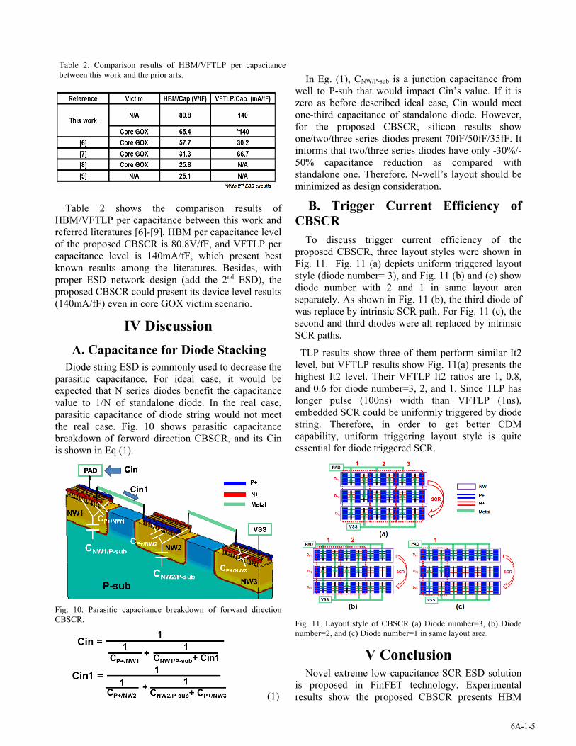
Table 2 shows the comparison results of HBM/VFTLP per capacitance between this work and referred literatures [6]-[9]. HBM per capacitance level of the proposed CBSCR is 80.8V/fF, and VFTLP per capacitance level is 140mA/fF, which present best known results among the literatures. Besides, with proper ESD network design (add the 2nd ESD), the proposed CBSCR could present its device level results (140mA/fF) even in core GOX victim scenario.
IV Discussion
A. Capacitance for Diode Stacking Diode string ESD is commonly used to decrease the
parasitic capacitance. For ideal case, it would be expected that N series diodes benefit the capacitance value to 1/N of standalone diode. In the real case, parasitic capacitance of diode string would not meet the real case. Fig. 10 shows parasitic capacitance breakdown of forward direction CBSCR, and its Cin is shown in Eq (1).
Fig. 10. Parasitic capacitance breakdown of forward direction CBSCR.
(1)
In Eg. (1), CNW/P-sub is a junction capacitance from well to P-sub that would impact Cin’s value. If it is zero as before described ideal case, Cin would meet one-third capacitance of standalone diode. However, for the proposed CBSCR, silicon results show one/two/three series diodes present 70fF/50fF/35fF. It informs that two/three series diodes have only -30%/-50% capacitance reduction as compared with standalone one. Therefore, N-well’s layout should be minimized as design consideration.
B. Trigger Current Efficiency of CBSCR
To discuss trigger current efficiency of the proposed CBSCR, three layout styles were shown in Fig. 11. Fig. 11 (a) depicts uniform triggered layout style (diode number= 3), and Fig. 11 (b) and (c) show diode number with 2 and 1 in same layout area separately. As shown in Fig. 11 (b), the third diode of was replace by intrinsic SCR path. For Fig. 11 (c), the second and third diodes were all replaced by intrinsic SCR paths.
TLP results show three of them perform similar It2 level, but VFTLP results show Fig. 11(a) presents the highest It2 level. Their VFTLP It2 ratios are 1, 0.8, and 0.6 for diode number=3, 2, and 1. Since TLP has longer pulse (100ns) width than VFTLP (1ns), embedded SCR could be uniformly triggered by diode string. Therefore, in order to get better CDM capability, uniform triggering layout style is quite essential for diode triggered SCR.
Fig. 11. Layout style of CBSCR (a) Diode number=3, (b) Diode number=2, and (c) Diode number=1 in same layout area.
V Conclusion Novel extreme low-capacitance SCR ESD solution
is proposed in FinFET technology. Experimental results show the proposed CBSCR presents HBM
Table 2. Comparison results of HBM/VFTLP per capacitance between this work and the prior arts.
6A-1-5

80.7V/fF and VFTLP It2 140mA/fF. Such high ESD robustness per capacitance results could effectively meet high speed serial link circuit requirements.
References [1] Fulde, et al., “Advances in multi-gate MOSFET
circuit design,” in International Conference on Electronics and Communication Systems (ICECS), 2007, pp. 186-189.
[2] Chang-Yun Chang, et al., “A 25-nm gate-length FinFET transistor module for 32nm node,” in International Electron Devices Meeting (IEDM), 2009, pp. 293-296.
[3] D. Linten, et al., "ESD in FinFET technologies: past learning and emerging challenges," in International Reliability Physics Symposium (IRPS), 2013, .
[4] S.-H. Chen et al., “Exploring ESD challenges in sub-20-nm bulk FinFET CMOS technology nodes”, EOS/ESD Symposium, 2013.
[5] A. Griffoni, et al., "Next generation bulk FinFET devices and their benefits for ESD robustness," EOS/ESD Symposium, 2009.
[6] Y.-T. Su, et al., “High CDM resistant low-cap SCR for 0.9V advanced CMOS technology,” EOS/ESD Symposium, 2013.
[7] T.-H. Chang, et al., “High-k metal gate-bounded silicon controlled rectifier for ESD protection,” EOS/ESD Symposium, 2012.
[8] J.-H. Lee, et al., “Two-stage trigger silicon-controller rectifier for radio-frequency (RF) ESD protection in the nanometer technologies,” in European Solid-State Device Research (ESSDERC), 2011, pp. 379–82.
[9] S. Thijs, et al., “On gated diodes for ESD protection in bulk FinFET CMOS technology,” EOS/ESD Symposium, 2011.
6A-1-6