700 ieee transactions on microwave theory … · modeling and design aspects of millimeter-wave and...
TRANSCRIPT

700 IEEE TRANSACTIONS ON MICROWAVE THEORY AND TECHNIQUES, VOL. 48, NO. 4, APRIL 2000
Modeling and Design Aspects of Millimeter-Waveand Submillimeter-Wave Schottky Diode
Varactor Frequency MultipliersJesús Grajal, Viktor Krozer, Member, IEEE, Emilio González, Francisco Maldonado, and Javier Gismero
Abstract—Design and optimization of Schottky varactordiode frequency multipliers for millimeter and submillimeterwavelengths are generally performed using harmonic balancetechniques together with equivalent-circuit models. Using thisapproach, it is difficult to design and optimize the device and mul-tiplier circuit simultaneously. The work presented in this paperavoids the need of equivalent circuits by integrating a numericalsimulator for Schottky diodes into a circuit simulator. The goodagreement between the calculated and published experimentaldata for the output power and conversion efficiency originatesfrom the accurate physical model. The limiting effects of multi-plier performance such as breakdown, forward conduction, orsaturation velocity are discussed in view of the optimum circuitconditions for multiplier operation including bias point, inputpower, and loads at different harmonics. It is shown that the onsetof forward or reverse current flow is responsible for the limitationin the conversion efficiency.
Index Terms—Frequency multipliers, harmonic balancetechnique, numerical modeling, Schottky diode modeling, semi-conductor simulation, submillimeter-wave multipliers.
I. INTRODUCTION
V ARACTOR frequency multipliers play a vital role indeveloping all-solid-state power sources at terahertz fre-
quencies. The key points in the progress of the performance ofSchottky varactor frequency multipliers have been the enhancedphysical insight into and optimization of submillimeter-waveSchottky diode operation [1], the improvement in frequencymultiplier analysis methods since the original work of Siegeland Kerr [2]–[5], and in physical analytical Schottky diodemodels [5]–[9], as well as numerical physical device models[4], [10]–[12]. The performance of active devices is defined notonly by their inherent characteristics, but also by the embeddingcircuit. This coupling can be taken into account by includinga numerical physical model into a circuit simulator [10], [11],[13]. The main problem in frequency varactor circuit designtoday is the inability to reproduce the experimental results
Manuscript received March 4, 1999. This work was supported in part by theEuropean Space Agency. The work of J. Grajal was supported by the ComunidadAutónoma de Madrid. The work of V. Krozer was supported by the Ministerio deEducación y Cultura Madrid, Spain, under the Programa Nacional de Formaciónde Personal Investigador.
J. Grajal, E. González, F. Maldonado, and J. Gismero are with the ETSIT,Technical University of Madrid, 28040 Madrid, Spain.
V. Krozer is with the Technical University of Chemnitz, D-09126 Chemnitz,Germany.
Publisher Item Identifier S 0018-9480(00)02529-1.
without additional empirical parameters. Furthermore, thelimitations of multiplier operation at high powers and/or highfrequencies is not well understood. Finally, a predictive designand circuit analysis tool is still missing, which is essential forthe design of integrated frequency multipliers.
The scope of this paper is to present a circuit analysis tool,which works without empirical parameters and is able to pre-dict the required device and circuit parameters of a frequencymultiplier. We focus on the circuit design and operation aspectsof frequency multipliers for millimeter and submillimeterbands. As a design tool, we employ the harmonic balancemethod (HBM) together with a physics-based drift-diffusion(DD) numerical device simulator. Our simulator incorporatesaccurate boundary and interface conditions for high forward aswell as reverse bias, including impact ionization, nonconstantrecombination velocity, self-consistent incorporation of thetunnelling, and image-force effects [11]. The validation of thenumerical simulator has been performed by comparison ofsimulated device and circuit characteristics with experimentalresults obtained for submillimeter-wave Schottky diodes fabri-cated at the Technical University Darmstadt (TUD), Darmstadt,Germany, and the University of Virginia (UVa), Charlottesville,and for a number of multiplier circuits published in the litera-ture [4], [5].
The integration of numerical simulators for active devicesinto circuit simulators avoids the need of an equivalent-circuitmodel extraction. This new philosophy accounts for the de-vice–circuit interaction and provides another degree of freedomto improve the performance of circuits because they can bedesigned from both a device and circuit point-of-view.
The simulation tool utilized in this paper and its implementa-tion are presented in Section II. The validation of the tool is out-lined in Section III, including a comparison of measured dc andRF performance characteristics with simulated values. In Sec-tion IV, an analysis of the performance of the frequency multi-pliers is presented together with an identification of the limitingmechanisms. Simulated results and a detailed discussion for thelimiting mechanisms are provided in Section V, including break-down and velocity saturation effects. Based on these results, thesynthesis of an optimum doubler and tripler circuit is dealt within Section VI. The optimization of the device parameters suchas doping concentration and profile, layer thicknesses, etc. areomitted in this paper, but will be dealt with in a future paper.This paper concludes with a summary of the results.
0018–9480/00$10.00 © 2000 IEEE
GRAJAL et al.: MODELING AND DESIGN ASPECTS OF SCHOTTKY DIODE VARACTOR FREQUENCY MULTIPLIERS 701
II. SIMULATION TOOL BASED ONPHYSICAL DEVICE MODEL
The HBM is the most common technique for the design oflarge-signal nonlinear microwave circuits. The HBM dependscritically on the accuracy of the nonlinear element modelemployed in the analysis. This model must be valid for a widerange of frequencies, drive levels, and embedding impedances.The electrical and RF performance characteristics of submil-limeter-wave Schottky diodes and frequency multiplier circuitsinvestigated here are based on an accurate physical model,which combines DD current transport with thermionic andthermionic-field emission currents imposed at the Schottkycontact.
The model for the carrier transport throughout the bulk isbased on an extended one–dimensional (1-D) DD formulation[14]. 1-D simulations are adequate for the current flow underthe Schottky metal, whereas two–dimensional (2-D) effects likecurrent spreading can be accounted for by analytical formulas.The governing equations are Poisson’s equation and continuityequations for electrons and holes as follows:
(1)
(2)
(3)
(4)
(5)
where is the electrostatic potential,is the permittivity, andare the electron concentration, hole concentration, and
ionized impurity donor concentration, respectively., , andare, respectively, the electron conduction current density, the re-combination rate modeled by the Schockley–Read–Hall recom-bination, and the generation rate currently restricted to impactionization [14]. Further, and represent the field-de-pendent electron mobility, temperature, affinity, and density ofstates in theconductionband, respectively.Similarequationsalsohold for holes. In (5), the conventional formulation of the posi-tion-dependent conduction band potential is augmented by theimage force term. In contrast to previous publications, we do notintroduce direct barrier lowering of the Schottky barrier height[15]. The simulation domain is divided into a nonuniform meshof approximately 100 mesh points and the simulation time is ofthe order of minutes for one frequency point.
A. Boundary and Interface Conditions
Dirichlet boundary conditions are imposed at all metalcontacts for Poisson’s and carrier continuity [14]. In thepresent model, thermionic and thermionic-field transport atthe Schottky barrier is introduced by means of an interfacecondition at the maximum of the barrier at the point [16].
The position of the maximum is no longer at the metallurgicalSchottky contact because of the influence of the bias-dependentimage force lowering. The interface condition for the carriertransport is based on the assumption that the carrier distributioncan be modeled by a displaced Maxwellian
(6)
Here, is the electron concentration at the maximumof the barrier and represents aquasi-equilibriumden-sity of electrons—the density that would be present at the top ofthe barrier if the electrons could be brought into thermal equi-librium without disturbing the potential distribution. is theclassical recombination velocity . is therecombination velocity after assuming a displaced Maxwellianshifted by a drift velocity
(7)
(8)
(9)
In this formulation, it has been assumed that the Schottky con-tact is located at . This interface condition prevents theunphysical effect of carrier accumulation at the interface [17],[18]. Between the point and the metallurgical contact, thepotential is assumed to vary linearly. No mesh points are re-quired here for the calculation of the potential and current den-sities. Newton’s method, Gummel’s method, as well as a hybridNewton/Gummel solution method are used for the solution of(1)–(5) with the interface conditions given in (6)–(9).
Tunnelling transport through the barrier is important forSchottky diodes with high doping in the epitaxial layer. Inour model, the time-independent Schrödinger equation issolved for arbitrary piecewise-linear potential barriers usingthe transfer matrix approach [19], [20]. The grid defined forPoisson’s equation is also used for Schrödinger’s equationin the volume of the device, but a number of additional gridpoints are generated between and the metallurgical contactin order to accurately resolve the shape of the conduction bandin this region. The new expression for the current density canbe represented by a simple integration [21] if the transmissioncoefficient is independent of the transversalcomponent of the kinetic energy and the distributionfunction is of Maxwellian type for the transversal componentof the kinetic energy
(10)
(11)
where is the Richardson constant, is the lattice tempera-ture (carrier heating is not considered), is the trans-

702 IEEE TRANSACTIONS ON MICROWAVE THEORY AND TECHNIQUES, VOL. 48, NO. 4, APRIL 2000
Fig. 1. Schematic drawing of the partitioning of the physical model and linear circuit for the harmonic balance calculations.
mission coefficient for the tunnelling transport, is the energyfor the normal component of the carrier velocity,and arethe electron distributions in the semiconductor and metal, re-spectively, stands for the conduction band in the semicon-ductor, and is the Fermi level in the metal. We have as-sumed that is a displaced Maxwellian distribution and isa Maxwell–Boltzmann distribution. If tunnelling is not consid-ered, this equation is similar to that proposed in [16].
B. Coupling the Physical Device Model with CircuitSimulation
Active devices are usually modeled as lumped equivalent cir-cuits in commercial harmonic balance codes. There exist sev-eral algorithms for the HBM [2], [22], [23], some of which havebeen specifically designed to deal with physical device simula-tors [24]. The selected algorithm for this study is based on thesolution of a system of nonlinear equations using a modifiedNewton’s algorithm or Powell’s algorithm, or the optimizationof an error function by using the Levenberg–Marquardt (LM)algorithm [25]. The LM algorithm is utilized in the current sim-ulations because of its efficiency.
In our case, the linear circuit is represented by the generalcoupling matrix, defined by network parameters, andthe generator impedance , as can be depicted in Fig. 1.
The harmonic balance error equation for each harmonicisthen
for
(12)
where
(13)
(14)
are the phasors of the excitations, andand are the har-monic components of the current and voltage at the diode termi-nals. In the case of frequency multipliers,is comprised of thedc voltage component and a single sinusoidal signal. The diodeis always matched at the fundamental frequency. Six to twelveharmonics are considered in these simulations, and the imped-ances at the higher harmonics are set to 0.001for both theresistive and reactive components, if not otherwise specified.
Fig. 2. Measured current voltage characteristic of a varactor Schottky diodecompared to simulated values for the diode D1038 from TUD. The diodeparameters are indicated in Table I.
All the parasitic elements of the diode are absorbed in theembedding network and included in the impedance seen by thejunction at the different frequencies involved in the multiplieroperation.
III. V ALIDATION OF THE PHYSICAL MODEL
The physical model has been validated with measurementsfor a large number of diodes in the doping range of
cm cm , different epitaxial layer thick-nesses and various diode diameters ranging from 1m 20 m.The simulated current voltage characteristic for all diodes agreeexcellently with the respective measurements. An example isgiven in Fig. 2 for the diode D1038. The parameters of all thediodes analyzed in this paper are provided in Table I.
The contribution of the individual components to the totaldiode current is indicated in Fig. 2. The simulated capacitancevoltage characteristic is also in excellent agreement with themeasured values, as demonstrated in Fig. 3. The simulation isextended up to the breakdown voltage, where the junction ca-pacitance is known to increase rapidly with reverse voltage [26].
The RF performance of the simulation tool has been dis-cussed in [12]. We have performed simulations for two fre-quency multipliers published in the literature [4], [5]. In the sim-ulations, we do not use any fitting parameters. In all simulations,a barrier height for the Schottky contact of eVis assumed.
The output power and efficiency versus the input power havebeen plotted in Fig. 4 for a frequency doubler (2100 GHz)

GRAJAL et al.: MODELING AND DESIGN ASPECTS OF SCHOTTKY DIODE VARACTOR FREQUENCY MULTIPLIERS 703
TABLE ISCHOTTKY DIODE PARAMETERS FOR
DEVICES FROMTUD AND UVa
Fig. 3. Comparison between the measured (symbols) and calculated (solidlines) capacitance voltage characteristic for two diodes from the TUD D1038and D734. The diode parameters are indicated in Table I.
utilizingaUVa6P4Schottkyvaractor.Theresultshavebeentakenfrom [4] with additional simulations achieved with our model(solid line with “ ” symbols). The techniques used in Fig. 4 areindicated as: 1) MCHB: self-consistent ensemble Monte Carloharmonic balance simulator; 2) DDHB-fdm: drift-diffusion har-monic balance simulator withfield-dependent mobility; and 3)DDHB-am: drift-diffusion harmonic balance with constantav-eragemobility.All simulatorsoverestimate theoutputpower [seeFig.4(a)] and the efficiency [seeFig.4(b)]of the doubler at
dBm.Results from ourmodelagree well above dBmand reproduce the measured power slope. The bias voltage was
V, and the loads at harmonic frequencies were set tofor , while at the fundamental fre-
quency, the diode wasmatched.The load impedanceat the outputwasoptimizedformaximumoutputpowerforeachinput
power and obeys a value of at an inputpower dBm. The unrealistic simulated results at lowinput powers originate fromthe perfect matchof the diode at eachpower level in contrast to the experimental setup, where the loadshave been optimized for high-power levels.
This is emphasized in Fig. 4(b), which shows that the resultsfrom the Monte Carlo code predict efficiencies close to the the-oretical limit at low input power levels, whereas the measuredefficiency is low and increases with power level. In our simula-
(a)
(b)
Fig. 4. (a) Calculated and measured output power and (b) conversionefficiency as a function of the input power for a frequency doubler atf = 100
GHz [4]. The solid line with symbols “+” denotes the results from our model,the solid line shows the experimental results from [4], and the dashed linesrepresent calculated results from [4].
tions, we have used the geometrical area and it is outlined belowthat our results would still improve when an effective diode areawould have been employed.
We have also compared our simulations with the mea-sured data for a frequency multiplier using a similar diodeat GHz [5], illustrated in Fig. 5. At the output, thebalanced diode configuration has been simulated as a directparallel connection of two identical diodes. The agreementwith measured data is very good. Simulations of the samearrangement at GHz also agree well at high-inputpower levels. Although the simulations presented in Figs. 4and 5 have been performed at different frequencies and withdifferent circuit structures, we achieve very good agreement atlarge power levels, which demonstrates the capabilities of thesimulation tool.
IV. A NALYSIS OF VARACTOR-BASED MULTIPLIER CIRCUITS
The results from a successful circuit analysis of frequencymultipliers should predict the following parameters determining

704 IEEE TRANSACTIONS ON MICROWAVE THEORY AND TECHNIQUES, VOL. 48, NO. 4, APRIL 2000
(a)
(b)
Fig. 5. (a) Calculated and measured output power and (b) conversionefficiency as a function of the input power for a frequency doubler atf = 80 GHz [5]. The symbols “�” “*” denote the results from our model atf = 80 GHz andf = 160 GHz, respectively, and the solid line shows theexperimental results from [5].
the multiplier performance for a given diode structure: outputpower , conversion efficiency , embedding impedancesat the fundamental, output, and idler frequencies at the diodeterminals, bias voltage , and load impedances at theremaining harmonics. All conventional multiplier designmethods are based on an equivalent circuit of the Schottkydiode presented in Fig. 6(a) [1], [2], [27]. However, this simplemodel cannot explain the decrease in conversion efficiencybeyond a certain input power level, which has been frequentlyobserved in experimental results. Improved intrinsic diodemodels have to be utilized in this case, as shown in Fig. 6(b)and (c), which describe the physical behavior of the device withincreasing accuracy. As has been pointed out by Grajalet al.[12], at low-input powers equivalent-circuit models, includingelectron velocity saturation phenomena [see Fig. 6(b)] aresufficient to accurately predict the multiplier performance.However, at high-power levels and near the maximum of theconversion efficiency, only accurate physical models [see
(a)
(b)
(c)
Fig. 6. Equivalent circuits for different Schottky diode varactor models. (a)Constant series resistance model. (b) Variable series resistance model. (c)Proposed physical model including all effects.
Fig. 6(c)] provide reasonable prediction of the multiplierperformance.
In Fig. 6(a) and (b), the Schottky junction is modeled bya parallel connection of a voltage-dependent nonlinear capac-itance and resistance. The series resistance due to the unde-pleted region in the semiconductor becomes a nonlinear func-tion of the diode current density at increased current densities[see Fig. 6(b)]. The nonlinear current dependent series resis-tance has been considered responsible for the decrease in theconversion efficiency at high-power levels [1], [5], [27]. It hasbeen argued that the displacement current becomes comparableto the maximum current in the material at high operating fre-quencies. An empirical current-dependent series resistance hasbeen introduced in order to fit the measured results, according toFig. 6(b). It has to be emphasized that the above analysis did notinclude breakdown effects and its impact on the RF operation ofthe frequency multiplier. Furthermore, the series resistance in-creases when the current density in the diode approaches themaximum current density
(15)
with being the displacement current. Dividing both sidesby the available number of electrons yields the maximum ve-locity with which the edge of the depletion region can move
(16)

GRAJAL et al.: MODELING AND DESIGN ASPECTS OF SCHOTTKY DIODE VARACTOR FREQUENCY MULTIPLIERS 705
Fig. 7. Efficiency, output power, and dc current atV = �3V for the D734varactor Schottky diode.
where is the width of the depletion region. Hence, (16) isequivalent to the argument that the displacement current den-sity must be less than the maximum current density in the semi-conductor in the undepleted region . It cannot beequal to the maximum current density because this would as-sume a zero conduction current in the depletion region.
The equivalent-circuit models require a separation of phys-ical effects into individual equivalent-circuit elements, an ex-traction of the equivalent-circuit element values from measure-ments distinct from the operating conditions, and an identifica-tion of equivalent-circuit elements with combined effects at highpowers and high frequencies, which is very difficult to achieve.
Therefore, a physical model is proposed, which is based onresults from the previous section. Such an approach enables usto concurrently optimize the device electrical and geometricalparameters together with attainable output power, conversionefficiency, and the required loads at the specific harmonics.
Although we agree that the current saturation mechanismbecomes important at very high frequencies, typically above300-GHz fundamental frequency, but it has only a marginaleffect on efficiency decrease at frequencies below 200 GHz,which were considered in [1]. The diode 6P4 shows velocitysaturation effects only because of its very low doping concen-tration in the epitaxial layer. We suggest that the limitation invaractor operation is due to the initiation of varistor operationwith a concurrent onset of dc current flow at either end ofthe current–voltage characteristic. For example, we have usedthe Schottky varactor diode D734 from TUD, similar to thediode 2T2 from UVa for simulations of frequency doublers andtriplers with our simulation tool. It can be inferred from Figs. 7and 8 that the maximum conversion efficiency coincides withthe onset of the dc current through the diode. In Fig. 7, the dccurrent is positive due to forward conduction, as can be depictedfrom the time-domain waveforms given in Fig. 9. In contrastto this, the dc current component in Fig. 8 is negative, origi-nating from impact ionization when the total voltage exceedthe breakdown voltage in the device, as indicated in Fig. 10.Independently of dc current polarity, the maximum of the
Fig. 8. Efficiency, output power, and dc current atV = �7 V for the D734varactor Schottky diode.
Fig. 9. v (t) andi (t) versus time forV = �3 V for the D734 varactorSchottky diode. Operating frequency isf = 50 GHz. The time scale is 32points per period.
conversion efficiency coincides with the onset of current flow,whereas the output power further increases with increasinginput power. The increase in output power is due to the mixedvaractor/varistor operation and the decrease in the efficiencyat high-power levels originates from the conversion of the RFsignal into dc power. The dc power is then delivered to thecircuit or dissipated in the device, respectively. It is important toobserve that the input power level for maximum efficiency doesnot coincide with the power level for maximum output power.Fig. 11 shows that, at low input power levels, the efficienciesfor the bias voltage V and V are nearlyequal. The reason is that the capacitance is nearly constantfor voltages lower than 7 V. Hence, no effective capacitancemodulation takes place for the negative semicycles. The slightincrease in the capacitance for V has an effect onthe tripler performance, but the doubler circuit is insensitive tothis small variation. Hence, the results for the efficiency of thedoubler circuit are very similar for these two bias conditions.Similar results have been obtained for the the tripler circuit, asindicated in Fig. 12.

706 IEEE TRANSACTIONS ON MICROWAVE THEORY AND TECHNIQUES, VOL. 48, NO. 4, APRIL 2000
Fig. 10. v (t) andi (t) versus time forV = �7V for the D734 varactorSchottky diode. Operating frequency isf = 50 GHz. The time scale is 32points per period.
Fig. 11. Frequency-doubler conversion efficiencies and output powers withD734 diode for three different bias conditionsV = �3 V, V = �5 V,V = �7 V. Operating frequency isf = 50 GHz.
V. MECHANISMS AND PARAMETERS LIMITING MULTIPLIER
PERFORMANCE
There exist three major mechanisms responsible for thelimitation of the output power and conversion efficiency:forward conduction, reverse breakdown, velocity saturation.These mechanisms have a direct impact on the muliplier circuitperformance such as the bias point, the maximum voltageswing, embedding impedances, and the load impedances atthe higher harmonics. The forward conduction mechanism isindependent of frequency and restricts the positive voltageswing of the sinusoidal signal at the device terminals. Thereverse breakdown mechanism is frequency dependent andlimits the signal excursion in the reverse direction. It can alsolead to current saturation in a well-designed diode by theincreased current flow due to impact ionization.
Fig. 12. Frequency-tripler conversion efficiencies and output powers withD734 diode for two different bias conditionsV = �5 V andV = �7 V.Operating frequency isf = 50 GHz.
Fig. 13. Calculated output power and conversion efficiency as a function ofthe input power for two TUD D734 Schottky varactors. The bias voltage isV = �5 V and optimum loads are chosen at the second and third harmonic.The fundamental frequency isf = 50 GHz. The symbols “*” are for a diodediameter of 6.7�m and the symbols “�” stand for results with a diode diameterof 13.4�m.
A. Impact of the Bias Point and the Series Resistance onMultiplier Performance
It should be observed in Fig. 11 that the output power levelsfor all bias conditions ultimately converge to similar values,however, with high dc currents. Operating the diodes at high dccurrents is not desirable due to reliability and burnout problemsassociated with high-current high-voltage operation. Therefore,the bias point for maximum conversion efficiency for a partic-ular diode is the point with maximum RF amplitude excursionwithout dc current generation, as ,where is the diffusion voltage and V isthe RF breakdown voltage for D734. The maximum conversionefficiency can also be shifted with regards to the input powerby utilizing Schottky diodes with different areas. Fig. 13 illus-trates calculated results for two Schottky varactor diodes D734with different anode diameters. The maximum conversion effi-ciency is shifted toward lower values of the input power when

GRAJAL et al.: MODELING AND DESIGN ASPECTS OF SCHOTTKY DIODE VARACTOR FREQUENCY MULTIPLIERS 707
Fig. 14. Variation of the real part of the diode impedance calculated from thephysical model as a function of the input power at bias voltagesV = �3 V,�5 V, �7 V for the diode from Fig. 7.
the diode area is decreased. The demand for maximum conver-sion efficiency at a prescribed input or output power uniquelydetermines the diode area. The optimum value is a function ofthe doping concentration, frequency, and desired output power.Highest output powers are achieved with large anode diametersbecause the output power and displacement current both scalewith the area. Whenever sufficient power is available to pumpthe diode up to maximum conversion efficiency and an appro-priate matching is realizable, a large-area diode will provide im-proved output power performance.
As demonstrated in [1] from DD physical calculations, thereal part of the diode impedance rises strongly with input powerlevel. We can reproduce this increase, which is illustrated inFig. 14 for the diode used in Figs. 7–10. Note that, in the caseof reverse breakdown, the real part of the diode impedance in-creases dramatically by a factor of more than 12. Such largechanges in the series resistance cannot be solely attributed tolowering of the mobility. One possible reason is that, at re-verse breakdown, the total diode resistance never reaches thezero-bias series resistance values due to the high fields in thespace–charge region. The interpretation of the numerical resultsin Fig. 14 in terms of equivalent-circuit elements is not simpleand the identification of the individual mechanisms with partic-ular equivalent-circuit elements is almost impossible in the caseof breakdown. In this case, the physical model should be usedfor the accurate characterization of the diode.
B. Impact of Breakdown Effect on Different OperatingConditions
As pointed out above, the generation of charges due to im-pact ionization plays a vital role in multiplier performance. Themodel for the generation of carriers due to avalanche multipli-cation is based on the following:
(17)
(18)
where and stand for the ionization coefficients for elec-trons and holes, and are the electron and hole current den-sities, and indicate empirical parameters for the calcu-lation of the ionization coefficients, is the electric field inthe space–charge region, and denotes the critical field forcharge generation, respectively. Some authors have pointed outthat the RF breakdown voltage is frequency dependent and canbe significantly different from the dc breakdown voltage [30],[31]. This has also been observed in our simulations. One pos-sible explanation for the frequency dependence is that, at highfrequencies, the conditions for avalanche are achieved for onlya short period of time and, therefore, the carriers in the mate-rial may not gain sufficient energy to ionize other carriers. Ad-ditionally, the carrier density does not follow the field changein unison because the carrier generationalso depends on thenumber of carriers already present, which is described through(2). This happens although the impact ionization rates in(17) follow the field change nearly instantaneously.
C. Velocity Saturation Mechanism at High Frequencies
High-frequency operation of frequency multipliers is limitedby the velocity saturation effect. It has been outlined in [32]that the current saturation mechanism should not occur forwell-designed diodes at all operating frequencies. This canbe achieved by choosing a sufficiently high doping density inthe device . The limited carrier velocityin materials such as GaAs determines the upper bound forthe rate of change of the space–charge width. Ultimately, thesignal frequency becomes larger than the maximum electronvelocity (for electrons in GaAs cm/s) andthe space–charge cannot be modulated. This is the case forthe 6P4 diode at frequencies around 100 GHz because of thelow doping concentration. At such high frequencies, otherfrequency-multiplying mechanisms or different materials likeInAs or InSb must be considered. It is shown in Fig. 15 that theedge of the depletion region can follow the voltage waveformat 100 GHz, but cannot follow the voltage waveform at 700GHz. In Fig. 15, the Schottky diode contact is located on theright-hand side of the diagram. It can be seen that the value formaximum depletion width m remains nearlyconstant for the three frequencies, whereas the differencebetween the minimum and maximum value of the depletionwidth decreases strongly with increasing frequencies.The decreased leads to a smaller modulation of thespace–charge region during one period of the exciting signal,which, in turn, leads to a smaller capacitance modulation. Thisasymmetry is probably due to the finite time required to emptythe space–charge region, while the space–charge region can berapidly filled with mobile charges. The transition between thespace–charge region and the undepleted region is abrupt at 100GHz and slopes with increasing frequencies.
The design procedure at high frequencies differs from that atlow frequencies because the breakdown voltage is no longer thelimiting factor. Hence, maximum output power and conversionefficiency is achieved when the current density is smaller thanthe saturation current [see (15)]. This determines the optimumdoping. The epi-layer thickness is then chosen for minimum

708 IEEE TRANSACTIONS ON MICROWAVE THEORY AND TECHNIQUES, VOL. 48, NO. 4, APRIL 2000
(a)
(b)
(c)
Fig. 15. Variation of the edge of the depletion region with applied RF voltageat (a) signal frequency of 100 GHz, (b) signal frequency of 500 GHz, and (c)signal frequency of 700 GHz. The epi-layer doping isN = 4 �10 /cm , theepi-layer thickness ist = 560 nm, diode diameter is 5�m.
series resistance. The circuit is operated at larger capacitancevalues (lower reverse bias).
VI. SYNTHESIS OFOPTIMUM FREQUENCYMULTIPLIERS
It has been demonstrated in [12] that the multiplier circuitis more sensitive to changes in the embedding impedances atlow-input power levels as compared to high-input power levels.This is independent of the diode considered in the simulations.
Fig. 16. Quality factorQ and the real part of the diode impedance<fZ (f )gas a function of input power for the diode 6P4. The operating conditions are thesame as in Fig. 4.
Fig. 17. Imaginary part of the diode embedding impedance=fZ (f )g as afunction of input power for the diode D734 for three different bias points.
The sensitivity can be defined in terms of a quality factor at therespective frequency
(19)
The real part of the diode impedance vary with input power andfrequency, whereas the imaginary part varies essentially only asa function of frequency. When the quality factoris large, thecircuit is more sensitive to changes in frequency.
The quality factor and the real part of the diode inputimpedance versus input power are illustrated in Fig. 16 for the6P4 diode. The imaginary part has been omitted because itchanges by less than 10% for all power levels. It can be seenthat at low-power levels belowdBm. For high-input power levels, the variation of the load isweak and all simulations show a strong increase of
in accordance with [1], [5].
GRAJAL et al.: MODELING AND DESIGN ASPECTS OF SCHOTTKY DIODE VARACTOR FREQUENCY MULTIPLIERS 709
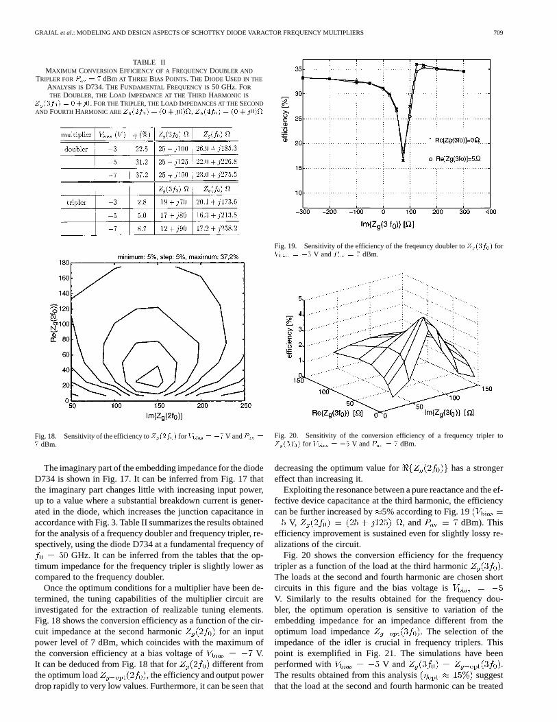
TABLE IIMAXIMUM CONVERSIONEFFICIENCY OF A FREQUENCYDOUBLER AND
TRIPLER FORP = 7 dBm AT THREEBIAS POINTS. THE DIODE USED IN THE
ANALYSIS IS D734. THE FUNDAMENTAL FREQUENCY IS50 GHz. FOR
THE DOUBLER, THE LOAD IMPEDANCE AT THE THIRD HARMONIC IS
Z (3f ) = 0+ |0. FOR THETRIPLER, THE LOAD IMPEDANCES AT THESECOND
AND FOURTH HARMONIC ARE Z (2f ) = (0 + |0),Z (4f ) = (0 + |0)
Fig. 18. Sensitivity of the efficiency toZ (2f ) forV = �7V andP =7 dBm.
The imaginary part of the embedding impedance for the diodeD734 is shown in Fig. 17. It can be inferred from Fig. 17 thatthe imaginary part changes little with increasing input power,up to a value where a substantial breakdown current is gener-ated in the diode, which increases the junction capacitance inaccordance with Fig. 3. Table II summarizes the results obtainedfor the analysis of a frequency doubler and frequency tripler, re-spectively, using the diode D734 at a fundamental frequency of
GHz. It can be inferred from the tables that the op-timum impedance for the frequency tripler is slightly lower ascompared to the frequency doubler.
Once the optimum conditions for a multiplier have been de-termined, the tuning capabilities of the multiplier circuit areinvestigated for the extraction of realizable tuning elements.Fig. 18 shows the conversion efficiency as a function of the cir-cuit impedance at the second harmonic for an inputpower level of 7 dBm, which coincides with the maximum ofthe conversion efficiency at a bias voltage of V.It can be deduced from Fig. 18 that for different fromthe optimum load , the efficiency and output powerdrop rapidly to very low values. Furthermore, it can be seen that
Fig. 19. Sensitivity of the efficiency of the freqeuncy doubler toZ (3f ) forV = �5 V andP = 7 dBm.
Fig. 20. Sensitivity of the conversion efficiency of a frequency tripler toZ (3f ) for V = �5 V andP = 7 dBm.
decreasing the optimum value for has a strongereffect than increasing it.
Exploiting the resonance between a pure reactance and the ef-fective device capacitance at the third harmonic, the efficiencycan be further increased by5% according to Fig. 19
V, , and dBm). Thisefficiency improvement is sustained even for slightly lossy re-alizations of the circuit.
Fig. 20 shows the conversion efficiency for the frequencytripler as a function of the load at the third harmonic .The loads at the second and fourth harmonic are chosen shortcircuits in this figure and the bias voltage isV. Similarly to the results obtained for the frequency dou-bler, the optimum operation is sensitive to variation of theembedding impedance for an impedance different from theoptimum load impedance . The selection of theimpedance of the idler is crucial in frequency triplers. Thispoint is exemplified in Fig. 21. The simulations have beenperformed with V and .The results obtained from this analysis suggestthat the load at the second and fourth harmonic can be treated

710 IEEE TRANSACTIONS ON MICROWAVE THEORY AND TECHNIQUES, VOL. 48, NO. 4, APRIL 2000
Fig. 21. Sensitivity of the conversion efficiency of a frequency tripler to theidler circuit Z (2f ) and to the load at the higher harmonicZ (4f ) forV = �5 V andP = 7 dBm.
independently and the impedance value at the idler frequencyis more important than the load at the fourth harmonic. Theresonance for the idler frequency requires inductive loads and,in the vicinity of the maximum efficiency, the sensitivity of theefficiency to variation in the impedance values is higher forincreasing values of .
In frequency doublers and triplers, the optimum load at thethird and fourth harmonic, respectively, does not depend on thepower level. A load different from short circuit at even higherharmonics has only a marginal effect on the multiplier perfor-mance.
VII. CONCLUSIONS
The degree of freedom that arises as a consequence of the cou-pling of a numerical model for Schottky diodes and a harmonicbalance circuit simulator has enabled us to study the differentoperation regimes and the physical limitations of the frequencymultiplier performances. It has also demonstrated its usefulnessto design multiplers from the circuit point-of-view: bias, inputpower, and loads at different harmonics.
We have obtained good agreement between published exper-imental results and our calculations for device and multipliercharacteristics operating at frequencies up to 320 GHz with ourenhanced DD model coupled to a harmonic balance simulator.
We have demonstrated that, at low input power levels, the op-eration of the multiplier is mainly determined by the embed-ding circuit and the choice for the dc operating point of thediode. The discrepancies observed in many simulation betweenthe measured and calculated results can be explained by mis-matching effects and do not originate from device physics. Incontrast, at high-power levels, the embedding circuit exhibitsonly minor contribution to the overall performance of the mul-tiplier and impact ionization in the device is responsible foroutput power saturation and conversion efficiency decrease athigh output powers.
It has been demonstrated that the onset of the dc current is re-sponsible for the decrease of the conversion efficiency at high-power levels. The impact of the breakdown effects, the velocitysaturation, and the forward conduction on frequency multiplier
performance has been discussed in detail. Simulated results sug-gest that the output power approaches similar values at highinput power independent of the choice of the bias point. At thesepower levels, the embedding circuit is determined by the in-crease of the real part of the input impedance. It was also foundthat an appropriate load at the high harmonics could improvethe efficiency independently from the power level.
ACKNOWLEDGMENT
The authors would like to thank C.-I. Lin and A. Simon, TUD,Darmstadt, Germany, for providing data on the varactor diodesfrom the TUD.
REFERENCES
[1] E. L. Kollberg, T. J. Tolmunen, M. A. Frerking, and J. R. East, “Currentsaturation in submillimeter wave varactors,”IEEE Trans. MicrowaveTheory Tech., vol. 40, pp. 831–838, May 1992.
[2] P. Siegel, A. R. Kerr, and W. Hwang, “Topics in the optimization of mil-limeter wave mixers,” NASA, CITY, STATE, NASA Tech. Rep. 2287,Mar. 1984.
[3] J. W. Archer, “Handbook of microwave and optical components,” inMultipliers and Parametric Devices, 2nd ed, K. Chang, Ed. New York:Wiley, 1990.
[4] R. E. Lipsey, S. H. Jones, J. R. Jones, T. W. Crowe, L. F. Horvath, U. V.Bhapkar, and R. J. Mattauch, “Monte Carlo harmonic-balance and drift-diffusion harmonic-balance analyzes of 100–600 GHz Schottky barriervaractor frequency multipliers,”IEEE Trans. Electron Devices, vol. 44,pp. 1843–1849, Nov. 1997.
[5] J. T. Louhi and A. V. Räisänen, “On the modeling and optimization ofSchottky varactor frequency multipliers at submillimeter wavelengths,”IEEE Trans. Microwave Theory Tech., vol. 43, pp. 922–926, Apr. 1995.
[6] , “Optimization of the Schottky varactor for frequency multiplierapplications at the submillimeter wavelengths,”IEEE MicrowaveGuided Wave Lett., vol. 6, pp. 241–242, June 1996.
[7] A. Jelenski, A. Grüb, V. Krozer, and H. Hartnagel, “New approach to thedesign and the fabrication of THz Schottky barrier diodes,”IEEE Trans.Microwave Theory Tech., vol. 41, pp. 549–557, Apr. 1993.
[8] K. East, “Monte Carlo simulation of Schottky barrier mixers and var-actors,” in Proc. 6th Int. Space Terahertz Technol. Symp., 1995, pp.442–446.
[9] V. Krozer and A. Grüb, “A novel fabrication technique and process sim-ulation by an analytical model for near-ideal epitaxial Pt/GaAs Schottkybarrier diodes,”Solid State Electron., vol. 37, no. 1, pp. 169–180, 1994.
[10] J. Grajal, V. Krozer, F. Maldonado, E. Gonzalez, C.-I. Lin, and H. L.Hartnagel, “Tripler circuit design with Schottky varactors,” inIEEE 6thInt. Terahertz Electron. Conf., Leeds, U.K., Sept. 4, 1998.
[11] J. Grajal, V. Krozer, E. González, J. Gismero, F. Maldonado, C. Lin, A.Simon, and H. L. Hartnagel, “Characterization of Schottky diode perfor-mance by numerical simulation coupled with harmonic balance,” in27thEuropean Microwave Conf., Jerusalem, Israel, Sept. 1997, pp. 190–195.
[12] J. Grajal, V. Krozer, and F. Maldonado, “Modeling and design aspectsof millimeter-wave Schottky varactor frequency multipliers,”IEEE Mi-crowave Guided Wave Lett., vol. 8, pp. 387–389, Nov. 1998.
[13] M. F. Zybura, J. R. Jones, S. H. Jones, and G. B. Tait, “Simulation of100–300 GHz solid state harmonic sources,”IEEE Trans. MicrowaveTheory Tech., vol. 43, pp. 955–961, Apr. 1995.
[14] S. Selberherr, Analysis and Simulation of Semiconductor De-vices. Berlin, Germany: Springer-Verlag, 1984.
[15] H. Hjelmgren, “Numerical modeling of hot electrons in n-GaAsSchottky-barrier diodes,”IEEE Trans. Electron Devices, vol. 37, pp.1228–1234, May 1990.
[16] R. B. Darling, “High field, nonlinear electron transport in lightly dopedSchottky-barrier diodes,”Sold State Electron., vol. 31, pp. 1031–1047,June 1988.
[17] J. O. Nylander, F. Masszi, S. Selberherr, and S. Berg, “Computer simu-lations of Schottky contacts with a nonconstant recombination velocity,”Solid State Electron., vol. 32, pp. 363–367, Aug. 1989.
[18] J. Adams and T. Tang, “A revised boundary condition for numericalanalysis of Schottky barrier diodes,”IEEE Electron Device Lett., vol.EDL-7, pp. 525–527, Sept. 1986.

GRAJAL et al.: MODELING AND DESIGN ASPECTS OF SCHOTTKY DIODE VARACTOR FREQUENCY MULTIPLIERS 711
[19] Y. Ando and T. Itoh, “Calculation of transmission tunneling cur-rent across arbitrary potential barriers,”J. Appl. Phys., vol. 1, pp.1497–1502, Feb. 1987.
[20] W. Lui and M. Fukuma, “Exact solution of the Schrödinger equationacross an arbitrary one-dimensional piecewise-linear potential barrier,”J. Appl. Phys., vol. 60, pp. 1555–1559, Sept. 1986.
[21] U. V. Bhapkar and R. J. Mattauch, “Numerical simulation of the current-voltage characteristics of heteroepitaxial Schottky-barrier diodes,”IEEETrans. Electron Devices, vol. 40, pp. 1038–1046, June 1993.
[22] V. Rizzoli and A. Neri, “State of the art and present trends in nonlinearmicrowave CAD techniques,”IEEE Trans. Microwave Theory Tech.,vol. 36, pp. 343–365, Feb. 1988.
[23] S. A. Maas,Nonlinear Microwave Circuits. Norwood, MA: ArtechHouse, 1988.
[24] G. B. Tait, “Efficient solution method for unified nonlinear microwavecircuit and numerical solid-state device simulation,”IEEE MicrowaveGuided Wave Lett., vol. 4, pp. 420–422, Dec. 1994.
[25] J. Gismero and J. Pérez, “Comparison of algorithms for the simulationof nonlinear circuits through the harmonic balance method,” inIEEEInt. Circuits Syst. Symp. Dig., Portland, OR, May 1989, pp. 594–597.
[26] J. S. Yuan and J. H. Ning, “Effect of impact ionization onc of het-erojunction bipolar transistors,”Solid State Electron., vol. 38, no. 3, pp.742–744, 1995.
[27] M. T. Faber, J. Chramiec, and M. E. Adamski,Microwave and Mil-limeter-Wave Diode Frequency Multipliers. Norwood, MA: ArtechHouse, 1995.
[28] A. Jelenski, A. Grüb, V. Krozer, and H. L. Hartnagel, “New approachto the design and the fabrication of the Schottky barrier diodes,”IEEETrans. Microwave Theory Tech., vol. 41, pp. 549–557, Apr. 1993.
[29] V. Krozer, “Verfahren der kleinsignal- und großsignal-analyse undcharakterisierung von mikrowellenschaltungen und bauelementen mithilfe der volterra-reihe,” Ph.D. dissertation, Dept. Elect. Eng., Tech.Univ. Darmstadt, Darmstadt, Germany, 1991.
[30] K. N. Ratnakumar, “Avalanche breakdown voltage of a microwave PINdiode,”Solid State Electron., vol. 19, pp. 656–657, 1975.
[31] J. M. Golio, Microwave MESFETs and HEMTs. Norwood, MA:Artech House, 1991.
[32] C.-I. Lin, V. Krozer, J. Grajal, A. Simon, and H. L. Hartnagel, “Schottkyvaractor diode optimization for frequency multipliers,” presented at the5th Int. Terahertz Electron. Workshop, Grenoble, France, Sept. 19, 1997.
[33] T. Crowe, T. C. Grein, R. Zimmermann, and P. Zimmermann, “Progresstoward solid-state local oscillators at 1 THz,”IEEE Microwave GuidedWave Lett., vol. 6, pp. 207–208, May 1996.
Jesús Grajalreceived the Ingeniero de Telecomuni-cación degree and Ph.D. degree from the TechnicalUniversity of Madrid, Madrid, Spain, in 1992, and1998, respectively.
In 1993, he joined the Signals, Systems andRadiocommunication Department, Technical Schoolof Telecommunication Engineering, Madrid, Spain,where he has been Associate Professor since 1998.His research activities are in the area of semicon-ductor simulation and high-frequency circuit design.
Viktor Krozer (M’93) received the Dr.-Ing. degreein electrical engineering from the Technical Univer-sity Darmstadt, Darmstadt, Germany, in 1991.
In 1991 he joined the Microwave Electronics Lab-oratory, Technical University Darmstadt, as a SeniorResearch Scientist in the area of microwave and tera-hertz electronics. Since 1996, he has been a Professorof electrical engineering at the Technical UniversityChemnitz, Chemnitz, Germany, and is currently theHead of the Microwave Electronics Laboratory. Hisresearch areas include physical modeling of semicon-
ductor devices, reliability of semiconductor devices, large-signal nonlinear mi-crowave circuits and submillimeter-wave devices and systems.
Emilio González received the Ingeniero de Teleco-municación degree from the Technical University ofMadrid, Madrid, Spain, in 1998.
He is currently with the Technical University ofMadrid. His research activities are in the area of semi-conductor simulation.
Francisco Maldonado received the Ingenierode Telecomunicatión degree from the TechnicalUniversity of Madrid, Madrid, Spain, in 1998.
He is currently with the Technical University ofMadrid. His research activities are in the area of semi-conductor simulation.
Javier Gismero received the M.S. and Ph.D.degrees in telecommunication engineering from thePolytechnic University of Madrid, Madrid, Spain, in1984 and 1989, respectively.
In 1985, he joined the Signals, Systems andRadiocommunication Department, Technical Schoolof Telecommunication Engineering, Madrid, Spain,where he has been Associate Professor since1989. His research activities are concerned withhigh-frequency device modeling and simulationand computer-aided design of integrated circuits in
hybrid and monolithic technologies.