70539_12a
TRANSCRIPT

MAGNETIC FIELD MEASUREMENT
MANFRED STECHER
Rhode & Schwarz GmbH &Co.KG
1. RELEVANCE OF ELECTROMAGNETIC FIELDMEASUREMENTS
The measurement of electromagnetic (EM) fields is rele-vant for various purposes: for scientific and technical ap-plications, for radio propagation, for electromagneticcompatibility (EMC) tests (i.e., testing of the immunityof electronic equipment to electromagnetic emissions aim-ing at the protection of radio reception from radio inter-ference), and for safety reasons (i.e., the protection ofpersons from excessive field strengths). For radio propa-gation and EMC measurements, below about 30 MHz adistinction is made between electric and magnetic compo-nents of the EM field to be measured. In the area of humansafety, this distinction is continued to even higher fre-quencies.
2. QUANTITIES AND UNITS OF MAGNETIC FIELDS
Especially in the measurement of radio propagation and ofradio interference, magnetic field measurements with loopantennas have traditionally been used to determine thereceived field intensity, which was quantified in units ofthe electric field strength, namely, in mV/m, respectively,in dB(mV/m). For radio propagation this can be justified forfar-field conditions where electric field strength E andmagnetic field strength H are related via the impedanceZ0 of the free space; E¼HZ0 (see also antenna factor def-inition). Commercial EMC standards in Refs. 1 and 2specify radiated disturbance measurements below30 MHz with a loop antenna; however, until 1990 mea-surement results and limits were expressed in dB(mV/m).Since this measurement is done at less than the far-fielddistance from the equipment under test (EUT) over a widefrequency range, the use of units of the electric fieldstrength was difficult to justify. Therefore, the CISPR(the International Special Committee on Radio Interfer-ence) decided in 1990 to use units of the magnetic fieldstrength mA/m, respectively, dB(mA/m).
Guidelines and standards for human exposure to EMfields specify the limits of electric and magnetic fields. Inthe low-frequency range (i.e., below 1 MHz [3]), limits ofthe electric field strength are not proportional to limits ofthe magnetic field strength. Magnetic field limits in fre-quency ranges below 10 kHz are frequently expressed inunits (T and G, for tesla and gauss) of the magnetic fluxdensity B despite the absence of magnetic material in hu-man tissue. Some standards specify magnetic field limitsin A/m instead of T (see Ref. 4 in contrast to Ref. 5). For
easier comparison with other applications we thereforeconvert limits of the magnetic flux density to limitsof the magnetic field strength using H¼B/m0 or1 T¼ 107=4pA=m � 0:796 . 106 A=m and 1 G¼ 79.6 A/m.At higher frequency ranges all standards specify limitsof the magnetic field strength in A/m. Above 1 MHz thelimits of the magnetic field strength are related to limits ofthe electric field strength via the impedance of the freespace. Nevertheless both quantities, electric and magneticfields, have to be measured, since in the near field theexposition to either magnetic or electric field may bedangerous.
3. RANGE OF MAGNETIC FIELD LEVELS TO BECONSIDERED FOR MEASUREMENT
In order to show the extremely wide range of magneticfield levels to be measured, we give limits of some nationalor regional standards. In different frequency ranges andapplications magnetic field strength limits vary from asmuch as 10 MA/m down to less than 1 nA/m (i.e., over 16decades). This wide range of field strength levels will nor-mally not be covered by one magnetic field meter. Differentapplications require either broadband or narrowbandequipment.
On the high level end there are safety levels and limitsof the magnetic field strength for the protection of personsthat vary from as much as 4 MA/m (i.e., 4�106 A/m cor-responding to the specified magnetic flux density of 5 T innonferrous material) at frequencies below 0.1 Hz, to lessthan 0.1 A/m at frequencies above 10 MHz (see Fig. 1)[3–6]. These limits of the magnetic field strength are de-rived from basic limits of the induced body current density(up to 10 MHz), respectively, basic limits of the specificabsorption rate (SAR, above 10 MHz). There are also
M
dB
(A/m
)
120
100
80
60
40
20
0
−20−30
130
0.1 10 1001.0 1 10110 100
MHzkHzHz
Figure 1. Safety limits of the magnetic field strength derivedfrom the European Prestandard ENV 50166 Parts 1 and 2:120 dB(A/m) are equivalent to 1 MA/m corresponding to 1.25 T,0 dB(A/m) are equivalent to 1 A/m.
2400

derived limits of the electric field strength which are how-ever not of concern here.
By using an approach different from the one of thesafety standards, the Swedish standard MPR II, whichhas become an international de-facto standard for video-display units (VDUs) without scientific proof, specifieslimits of the magnetic flux density in two frequency rang-es, which are bounded by filters: a limit of 40 nT(E0.032 A/m) in the range from 5 Hz to 2 kHz and a lim-it of 5 nT (E0.004 A/m) in the range from 2 kHz to400 kHz.
On the low-level end there are limits for the protectionof radio reception and electromagnetic compatibility insome military standards (see Figs. 2 and 3).
International and national monitoring of radio signalsand the measurement of propagation characteristics re-quire the measurement of low-level magnetic fields downto the order of –30 dB(mA/m): see also subsequent discus-sions and Refs. 7–9. For the protection of radio reception,international, regional (e.g., European) and national ra-diated emission limits and measurement procedures havebeen standardized for industrial, scientific, medical (ISM)and other equipment [1,2,10–12]. An example is given inFig. 4.
Radiated emission limits of fluorescent lamps andluminaires are specified in a dB(mA) using a large-loop-antenna system (LAS) [10]. For further information, seethe text below.
4. EQUIPMENT FOR MAGNETIC FIELD MEASUREMENTS
4.1. Magnetic Field Sensors Others than Loop Antennas
An excellent overview of magnetic field sensors other thanloop antennas is given in Ref. 13. Table 1 lists the differenttypes of field sensors that are exploiting different physicalprinciples of operation.
4.2. Magnetic Field Strength Meters with Loop Antennas
Especially for the measurement of radiowave propagationand radiated electromagnetic disturbance pickup devices,the antennas become larger and therefore are used sepa-rately from the indicating instrument (see Fig. 5). The in-strument is a selective voltmeter, a measuring receiver, ora spectrum analyzer. The sensitivity pattern of a loop an-tenna can be represented by the surface of two spheres(see Figs. 6 and 7). In order to determine the maximumfield strength, the loop antenna has to be turned into thedirection of maximum sensitivity.
To obtain an isotropic field sensor, three loops have tobe combined in such a way that the three orthogonal com-ponents of the magnetic field Hx, Hy, and Hz are combinedto fulfill the equation
30
25
20
15
10
5
0
−5
−10
−15
−200.15 1 10 30
dB
A
/m�
MHz
Figure 4. Radiated emission limits for navigational receiversaccording to draft revision IEC 945 (IEC 80/124/FDIS), originallygiven in dB(mV/m), for the purpose of this article converted intodB(mA/m).
160
140
120
100
80
60
40
170
0.03 0.1 1 10 100
dB
A
/m�
kHz
Figure 2. Magnetic field strength limits derived from U.S. MIL-STD-461D RE101 (Navy only) [7]. These limits are originally giv-en in dB(pT) (decibels above 1 pT). The measurement procedurerequires a 36-turn shielded loop antenna with a diameter of13.3 cm. Measurement distance is 7 cm for the upper limit and50 cm for the lower limit.
60
40
20
0
−20
−40
−60−70
0.01 0.1 1 10 30
dB
A
/m�
MHz
Figure 3. Narrowband emission limits of the magnetic fieldstrength derived from the German military standard VG95343 Part 22 [8]. This standard gives the limits of H �Z0 indB(mV/m) of four equipment classes, the emissions have to bemeasured with a loop antenna calibrated in dB(mV/m) in the nearfield of the equipment under test (EUT). Therefore, the limitshave been converted into dB(mA/m). The lower limits is Class 1,the upper is Class 4.
MAGNETIC FIELD MEASUREMENT 2401

H¼ffiffiffiffiffiffiffiffiffiffiffiffiffiffiffiffiffiffiffiffiffiffiffiffiffiffiffiffiffiffi
H2x þH2
y þH2z
q
Isotropic performance is, however, only a reality in broad-band magnetic field sensors, where each component is de-tected with a square-law detector and combinedsubsequently. For the measurement and detection of ra-dio signals isotropic antennas are not available. Hybridsmay be used for limited frequency ranges to achieve anomnidirectional azimuthal (not isotropic) pickup.
4.2.1. Antenna Factor Definition. The output voltage Vof a loop antenna is proportional to the average magneticfield strength H perpendicular to the loop area. If the an-tenna output is connected to a measuring receiver or aspectrum analyzer, the set consisting of antenna and re-ceiver forms a selective magnetometer.
The proportionality constant is the antenna factor KH
for the average magnetic field strength H:
KH ¼H
Vin
A
m
1
V¼
1
O .mð1aÞ
Table 1. Overview of Different Magnetic Field Sensors, their Underlying Physical Effects, their Applicable Level, andFrequency Ranges from Ref. 13a
Type Principles of Operation Level of Operation Frequency Range
Search coil magnetometer Faraday’s law of induction 10–6–109 A/m 1 Hz–1 MHzFlux gate magnetometer Induction law with hysteresis of mag-
netic material10–4–104 A/m DC–10 kHz
Optically pumped magne-tometer
Zeeman effect: splitting of spectrallines of atoms
10–6–102 A/m DC
Nuclear precession mag-netometer
Response of nuclei of atoms to a mag-netic field
10–5–102 A/m DC (upper frequency limited bygating frequency of hydrocar-bon fluid)
SQUID magnetometer Superconducting quantum interfer-ence device
10–8–10–2 A/m; speciality:differential field mea-surements
DC
Hall effect sensor Hall effect 10–1–105 A/m DC–1 MHzMagnetoresistive magne-
tometerMagnetoresistive effect 10–4–104 A/m DC–1 GHz
Magnetodiode Semiconductor diode with undopted sil-icon
10–2–103 A/m DC–1 MHz
Magnetotransistor Hall and Suhl effects 10–3–103 A/m DC–1 MHzFiberoptic magnetometer Mach–Zehnder interferometer 10–7–103 A/m DC–60 kHzMagnetooptical sensor Faraday polarization effect 102–109 A/m DC–1 GHz
aTo facilitate comparison with values given in text, the values from Ref. 13 have been converted from gauss to A/m.
Measuringreceiver
Network
ZLRi
r IX
Hav
Ri
Figure 5. Magnetic field strength measuring loop. The networkmay consist of a passive or active circuit.
E−x
Ex
P−z
P H
E
P H
E
Pz
Pz
Hy
I
I
H H
Hy H y
y
z
x
E−x
P−z
Hy
Hy
�
�
Ex n
Figure 6. Cross section of a loop antenna sensitivity pattern. Thearrow length Ha shows the indicated field strength at an angle awhich is a fraction of the original field strength H, with Ha¼
H cos a.
E−x
Ex
Ez
P−z
P−x
PHE
P
H
E P
H
H
E
P
H
E
Pz
H y
H y
H yH y
I
II
I
x
y
z
Figure 7. Direction of the field vectors (H, E and P) under far-field conditions.
2402 MAGNETIC FIELD MEASUREMENT
For the average magnetic flux density B the correspondingproportionality constant is
KB¼B
V¼
m0H
V¼ m0KH in
V . s
A .m
A
m
1
V¼
V . s
m2
1
V¼
T
V
ð1bÞ
In the far field, where electric field and magnetic fieldsare related via the free-space wave impedance Z0, theloop antenna can be used to determine the electricfield strength E. For this case the proportionality constantis
KE¼E
V¼
Z0H
V¼Z0KH in
V
A
A
m
1
V¼
1
mð1cÞ
In the area of radiowave propagation and radio distur-bance measurement, quantities are expressed in logarith-mic units. Therefore, the proportionality constants areconverted into logarithmic values, too:
kH ¼ 20 logðKHÞ in dB1
Om
� �
ð2aÞ
kB¼ 20 logðKBÞ in dBT
V
� �
ð2bÞ
kE¼ 20 logðKEÞ in dB1
m
� �
ð2cÞ
By using logarithmic antenna factors, a field strength lev-el 20 log(H) is obtained in dB(mA/m) from the measuredoutput voltage level 20 log(V) in dB(mV) by applying theequation: 20 log(H)¼ 20 log(V)þ kH. The final section ofthis article describes a method calibrate the antenna fac-tors of circular loop antennas.
4.2.2. Concepts of Magnetic Field Strength Meters. Theloop antenna of a magnetic field strength meter may bemounted on the measuring receiver (or used as a separateunit, connected to the measuring receiver) with a coaxialcable. CISPR 16-1, the basic standard for emission mea-surement instrumentation to commercial (i.e., nonmili-tary) standards, requires a loop antenna in the frequencyrange from 9 kHz to 30 MHz which is completely enclosedby a square having sides 0.6 m in length. For protectionagainst stray pickup of electric fields, loop antennas em-ploy a coaxial shielding structure. For optimum perfor-mance, the shielding structure may be arrangedsymmetrically in two half-circles around a circular loopwith a slit between the two halves in order to avoid electriccontact between the two shields.
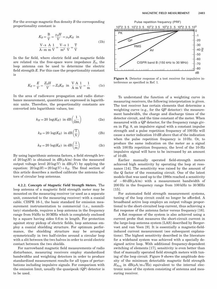
For narrowband magnetic field measurements of radiodisturbance, measuring receivers employ standardizedbandwidths and weighting detectors in order to producestandardized measurement results for all types of pertur-bations including impulsive signals. For comparison withthe emission limit, usually the quasipeak (QP) detector isto be used.
To understand the function of a weighting curve inmeasuring receivers, the following interpretation is given.The test receiver has certain elements that determine aweighting curve (e.g., for the QP detector): the measure-ment bandwidth, the charge and discharge times of thedetector circuit, and the time constant of the meter. Whenmeasured with a QP detector, for the frequency range giv-en in Fig. 8, an impulsive signal with a constant impulsestrength and a pulse repetition frequency of 100 Hz willcause a meter indication 10 dB above that of the indicationwhen the pulse repetition frequency is 10 Hz. Or, toproduce the same indication on the meter as a signalwith 100 Hz repetition frequency, the level of the 10-Hzimpulsive signal will have to be increased by an amountof 10 dB.
Earlier manually operated field-strength metersachieved high sensitivity by operating the loop at reso-nance [14]. The sensitivity was raised by the amount ofthe Q factor of the resonating circuit. One of the latestmodels that was used up to the 1980s reached a sensitivityof � 60 dB(mA/m) with a measurement bandwidth of200 Hz in the frequency range from 100 kHz to 30 MHz[15].
For automated field strength measurement systems,tuning of the loop circuit could no longer be afforded. Abroadband active loop employs an output voltage propor-tional to the short-circuited loop current, thus achieving aflat response of the antenna factor versus frequency [16].
A flat response of the system is also achieved using acurrent probe that measures the short-circuit current inthe large-loop antenna system [LAS] described by Berger-voet and van Veen [9]. It is essentially a magnetic-field-induced current measurement (see subsequent explana-tions). The highest sensitivity described in the literaturefor a wideband system was achieved with a specially de-signed active loop. With additional frequency-dependentswitching of elements [17], sensitivity is even better thanthat of manually operated field strength meters with tun-ing of the loop circuit. Figure 9 shows the amplitude den-sity of the minimum detectable magnetic field strengthHNeq in dBðmA=m
ffiffiffiffi
Hp
zÞ equivalent to the internal elec-tronic noise of the system consisting of antenna and mea-suring receiver.
0
−1
−20
−30
−40
−50
−60
−70
−80
PK
QP
AVRMS
CISPR band B (150 kHz to 30 MHz)
Hz
100 1012 3 5 2 3 5 102 2 3 5 1032 3 5 104 1052 3 5
Pulse repetition frequency (PRF)
dB
Figure 8. Detector response of a test receiver for impulsive in-terference as specified in Ref. 1.
MAGNETIC FIELD MEASUREMENT 2403

5. MAGNETIC FIELD STRENGTH MEASUREMENTMETHODS
5.1. Measurement of Magnetic Fields with Regard to HumanExposure to High EM Fields
Usually, to measure magnetic fields with regard to humanexposure to high fields, magnetic field strength meters areusing broadband detectors and apply an isotropic re-sponse. Modern concepts of low-frequency electric andmagnetic field strength meters apply fast Fourier trans-form (FFT) for proper weighting of the total field with re-gard to frequency-dependent limits [18,19].
5.2. Use of Loop Antennas for Radiowave Field StrengthMeasurements up to 30 MHz
ITU-R Recommendation PI.845-1 Annex 1 gives guidanceto accurate measurement of radio wave field strengths.Rod antennas are the preferred receiving antennas sincethey provide omnidirectional azimuthal pickup. The posi-tioning of vertical rod antennas is important, however,since the result is very sensitive to field distortions by ob-stacles and sensitive to the effects of ground conductivity.It is a well-known fact that measurements with loop an-tennas are less sensitive to these effects and their calibra-tion is not affected by ground conductivity apart from thefact that the polarization may deviate from horizontal ifground conductivity is poor. Therefore, many organiza-tions use vertical monopoles for signal measurements butstandardize results by means of calibration data involvingcomparisons for selected signals indicated by fieldstrength meters incorporating loop-receiving antennas.Accuracy requirements are given in Ref. 20, general in-formation on equipment and methods of radio monitoringare given in Ref. 21.
5.2.1. Solutions to Problem with Ambients in CommercialEMI Standards. CISPR Class B radiated emission limits inthe frequency range from 9 kHz to 30 MHz have been at34 dB(mV/m) at a distance of 30 m from the EUT for a longtime. Moreover, the test setup with EUT and vertical loopantenna required turning of both EUT and the loop an-tenna to find the maximum emission. On most of the
open-area test sites the ambient noise level makes com-pliance testing almost impossible. This is due to the factthat ambient noise itself is near or above the emissionlimit. Two different approaches were proposed as a solu-tion to that problem:
1. To reduce the measurement distance from 30 to 10 mor even 3 m. A German group proposed frequency-dependent conversion factors, justified by calcula-tions and an extensive amount of measurements.The conversion factors are given in Fig. 10. InFig. 10 the slopes between 1.8 and 16 MHz showthe transition region from near field, where H is in-versely proportional with r3 or r2.6, to far field,where H is inversely proportional with r.
2. To reduce the measurement distance to zero. ADutch group proposed the large-loop antenna sys-tem mentioned previously [9]. With this method theEUT is placed in the center of a loop antenna sys-tem, which consists of three mutually perpendicularlarge-loop antennas (Fig. 11). The magnetic fieldemitted by the EUT induces currents in the large-loop antennas. Since there are three orthogonalloops, there is no need to rotate either the EUT orthe loop antenna system. The current induced ineach loop is measured by means of a current probe,which is connected to a CISPR measuring receiver.Since the current is measured, emission limits aregiven in dB(mA) instead of dB(mA/m). Each loop an-tenna is constructed of a coaxial cable that containstwo slits, positioned symmetrically with respect tothe position of the current probe. Each slit is loadedby resistors in order to achieve a frequency responseflat to within 72 dB in the frequency range from9 kHz to 30 MHz [9,10]. In order to verify and vali-date the function of each large loop, a specially de-signed folded dipole has been developed [9,10]. It
70
60
50
40
30
20
10
0
dB
0.009 0.1 1 10 30
MHz
Figure 10. Conversion factors DH for the limit of the magneticfield strength from measurement distance 30 m to measurementdistances 10 and 3 m above a conducting ground plane accordingto Ref. 23. The upper curve is for 30–3 m; the lower curve is for 30–10 m distance.
Field-strength sensitivity (dB A/m Hz)�20
0
−20
−40
−60
−90
−100
Range 1
Range 2
Range 3
Range 4Range 5
100 1000 10000 105 106 107 108
Frequency (Hz)
Figure 9. Sensitivity per hertz bandwidth of the active loop [16].
2404 MAGNETIC FIELD MEASUREMENT

produces both a magnetic dipole moment mH and anelectric dipole moment mE, when a signal is con-nected to the folder dipole. The folded dipole servesto test large loop antenna for its sensitivity in eightpositions.
5.2.2. Problems in the Near-Field–Far-Field TransitionZone. Problems with magnetic field strength measure-ments in the transition region between near field andfar field are discussed in detail in Ref. 22. When a smallmagnetic dipole is located in the free space, the electro-magnetic field in a point P(r, y, j) is described by the fol-lowing three relations (see Fig. 12):
Hr¼jk
2pmH cos y
r21þ
1
jkr
� �
e�jkr ð3aÞ
Hy¼�k2
4pmH sin y
r1þ
1
jkr�
1
ðkrÞ2
� �
e�jkr ð3bÞ
Ej¼Z0k2
4pmH sin y
r1þ
1
jkr
� �
e�jkr ð3cÞ
where k¼ 2p/l and mH ¼ pR20I0 is the magnetic dipole mo-
ment, a vector perpendicular to the place of the dipole.Equations (3a)–(3c) completely describe the electromag-netic field of the magnetic dipole.
Two situations are discussed further: (1) the near field,where r is much smaller than l but larger than the max-imum dimension of the source (i.e., kr51); and (2) the farfield, where r is much larger than l and much larger thanthe maximum dimension of the source (i.e., krb1).
For the near-field case, where kr51 and using e–jkr¼
cos(kr)� j sin(kr), Eqs. (3a)–(3c) are simplified to
Hr¼2mH cos y
4pr3ð4aÞ
Hy¼mH sin y
4pr3ð4bÞ
Ej¼kZ0mH sin y
4pr2ð4cÞ
From Eqs. (4a)–(4c) we can see that Hr and Hy are in-versely proportional to r3, whereas Ej is inversely propor-tional to r2.
For the far-field case where krb1, Eqs. (3a)–(3c) arereduced to
Hr¼jkmH cos y
2pr2e�jkr ) 0 ð5aÞ
Hy¼�k2mH sin y
4pre�jkr ð5bÞ
Ej¼k2Z0mH sin y
4pre�ikr ð5cÞ
From Eqs. (5a)–(5c) one can see that in the far field Hr
vanishes in comparison to Hy and that Hy and Ej are in-versely proportional to r.
In the frequency range from 9 kHz to 30 MHz, whereemission limits have been set, the corresponding wave-length is 33 km–10 m. Since for compliance testing, ambi-ent emissions on an open-area test site require a reductionof the measurement distance to 10 m or even 3 m, mea-surements are carried out in the near-field zone over awide frequency range. At the higher frequency range thetransition zone and the beginning far field zone arereached. Goedbloed [22] investigated the transition zoneand identified the critical condition where Hr and Hy areequal in magnitude. It occurs where
2mH
4pr3
ffiffiffiffiffiffiffiffiffiffiffiffiffiffiffiffiffiffi
1þ k2r2p
¼mH
4pr3
ffiffiffiffiffiffiffiffiffiffiffiffiffiffiffiffiffiffiffiffiffiffiffiffiffiffiffiffiffiffiffiffi
1� k2r2þ k4r4p
ð6Þ
or where
fr¼ 112:3 in MHz .m ð7Þ
For r¼10 m, Hymax4Hrmax at frequencies greater than11 MHz.
Coaxial-switch
To testreceiver
Ferriteabsorbers
EUT
Currentprobe
Figure 11. Simplified drawing of a large-loop antenna systemwith position of the EUT.
y
z
x
H r
I o
Ro
E�
�
� H�r
P
0
Figure 12. Field components Hr, Hy, and Ej in P at a distance rfrom the center of the magnetic dipole in the xy plane.
MAGNETIC FIELD MEASUREMENT 2405

The CISPR magnetic field measurement method is il-lustrated in Fig. 13, with the test setup on a metallicground plane and the receiving antenna in the verticalplane. In Figs. 14 and 15, two different cases of radiatingelectrically small magnetic dipoles are illustrated; the firstone, with the dipole moment parallel to the ground planeand the second one, with the dipole moment perpendicularto the ground plane. Because of the reflecting groundplane two sources are responsible for the field at the loca-tion of the receiving antenna: the original source and themirror source. The points and crosses drawn in both sourc-es show the direction of the current. In Fig. 14, the cur-rents are equally oriented. In this case the loop antennadetects the radial component Hd,r and the direct tangen-tial component Hd,y¼ 0 since yd¼ 0. Therefore, direct ra-diation will only contribute if fd5112 MHz �m [seeEq. (7)]. In the case of fdb112 MHz �m, the loop antennawill receive direct radiation if it is rotated by 901. This maybe observed frequently in practical measurements: at lowfrequencies the maximum radiation is found with loopantenna in parallel to the EUT and at high frequencieswith the loop antenna oriented perpendicular to the EUT.In addition to these direct components, the indirect radialand tangential components Hi,r and Hi,y are superposi-tioned in the loop antenna. Assuming near-field conditionsit follows from Eqs. (4), that the magnitude of the mag-
netic field Hm is given by
Hm¼Hd;rþHi;r cos yi �Hi;y sin yi
¼mH
4pd32þ
d3
d3i
ð2 cos2 yi � sin2 yiÞ
� � ð8Þ
where di¼
ffiffiffiffiffiffiffiffiffiffiffiffiffiffiffiffiffiffiffiffiffiffi
ð2hÞ2þd2
q
is the distance between the mirror
dipole and the loop antenna.Goedbloed gives a numerical example with mH¼
4p103 mA .m2 (e.g., 100 mA through a circular loop with adiameter of 0.40 m). Using Eq. (8) with d¼ 3 m and h¼1.3 m will give Hm¼ 38.6 dB(mA/m) with the mirror sourceand 37.4 dB(mA/m) without the mirror source, whichshows that in this case the reflecting ground plane haslittle influence. The influence of the ground plane is quitedifferent in the case of a vertical dipole moment, specifi-cally, a dipole moment perpendicular to the ground planeas illustrated in Fig. 15. In the case of Fig. 15 the loopantenna does not receive direct radiation at all, as Hd,r (yd
¼ p/2)¼ 0 and Hd,y is parallel to the loop antenna. Hence,the received signal is completely determined by the radi-ation coming from the mirror source, which also meansthat the result is determined by the quality of the reflect-ing ground plane. With the reflecting ground place Hm¼
Hi,r sin yiþHi,y cos yi¼27.2 dB(mA/m), whereas withoutthe reflecting ground plane no field strength will bemeasured. If the loop antenna were positioned horizontal-ly above the ground plane at h¼ 1.3 m, then Hm¼
Hd,yþHi,r cos yi�Hi,y sin yi¼ 32.4 dB(mA/m) and Hm¼
31.4 dB(mA/m) without the reflecting ground plane. Mea-surements in a shielded room would be even less predict-able, since the result would be determined by mirrorsources on each side, including the ceiling of the shieldedroom. Absorbers are not very helpful in the low frequencyranges. From the results, Goedbloed concludes that in or-der to judge the interference capability of an EUT, themethod proposed by Bergervoet and van Veen [9], is anefficient method of magnetic field measurements.
mH
mH d i
d
h
h
�
�H d,�
H i,r
H i,�
LA
Ground plane
(a)
(b)
i
Figure 15. (a) Receiving conditions for a magnetic dipole with avertical dipole moment, and the receiving loop antenna in thevertical position as specified by the standard; (b) vectors of theindirectly radiated H-field components (no reception of directradiation).
EUT
Turntable
0.8 m
Metallic groundplane
0.3 m
Loop antenna
To receiver1 m
Figure 13. Basic CISPR setup for magnetic field measurements.Both EUT and loop antennas have to be turned round until themaximum indication on the receiver has been found.
mH
mH
d i
d
h
h
�
H i,�
H d,r
H i,r LA
Ground plane
(a)
(b)
� i
Figure 14. (a) Receiving conditions for a magnetic dipole with ahorizontal dipole moment; (b) vectors of the directly and indirectlyradiated H-field components.
2406 MAGNETIC FIELD MEASUREMENT

6. CALIBRATION OF A CIRCULAR LOOP ANTENNA
A time-varying magnetic field at a defined area S can bedetermined with a calibrated circular loop. For narrow-band magnetic field measurements, a measuring loop con-sists of an output interface (point X on Fig. 5), which linksthe induced current to measuring receiver. It may have apassive or an active network between loop terminals andoutput. The measuring loop can also include a shieldingover the loop circumference against any perturbation ofstrong and unwanted electric fields. The shielding shouldbe interrupted at a point on the loop circumference.
Generally in the far field that streamlines of magneticflux are uniform, but in the near field, that is, in the vi-cinity of the generator of a magnetic field, they depend onthe source and its periphery. Figure 19 shows the stream-lines of the electromagnetic vectors generated by thetransmitting loop L1. In the near field, the spatial distri-bution of the magnetic flux, B¼ m0H, over the measuringloop area is not known. Only the normal components of themagnetic flux, averaged over the closed-loop area, can in-duce a current through the loop conductor.
The measuring loop must have a calibration (conver-sion) factor or set of factors, that, at each frequency, ex-presses the relationship between the field strengthimpinging on the loop and the indication of the measur-ing receiver. The calibration of a measuring loop requiresthe generation of a well-defined standard magnetic fieldon its effective receiving surface. Such a magnetic field isgenerated by a circular transmitting loop when a definedroot-mean-square (RMS) current is passed through itsconductor. The unit of the generated or measured mag-netic field Hav is A/m and therefore is also an RMS value.The subscript ‘‘av’’ strictly indicates the average value ofthe spatial distribution, not the average over a period of Tof a periodic function. This statement is important fornear-field calibration and measuring purposes. For far-field measurements the result indicates the RMS value ofthe magnitude of the uniform field. In the following wediscuss the requirements for the near-zone calibration of ameasuring loop.
7. CALCULATION OF STANDARD NEAR-ZONE MAGNETICFIELDS
To generate a standard magnetic field, a transmitting loopL1 is positioned coaxial and plane-parallel at a separationdistance d from the loop L2, as in Fig. 16. The analyticalformula for the calculation of the average magnetic fieldstrength Hav in A/m generated by a circular filamentaryloop at an axial distance d including the retardation due tothe finite propagation time was obtained earlier. The av-erage value of field strength Hav was derived from the re-tarded vector potential Aj as tangential component on thepoint P of the periphery of loop. L2:
Hav¼Ir1
pr2
Z p
0
e�jbRðjÞ
RðjÞcosðjÞdj ð9aÞ
RðjÞ¼ffiffiffiffiffiffiffiffiffiffiffiffiffiffiffiffiffiffiffiffiffiffiffiffiffiffiffiffiffiffiffiffiffiffiffiffiffiffiffiffiffiffiffiffiffiffiffiffiffiffiffiffiffiffiffiffiffi
d2þ r21þ r2
2 � 2r1r2 cosðjÞq
ð9bÞ
In these equations for the thin circular loop, I is trans-mitting loop RMS current in amperes, d is distance be-tween the planes of the two coaxial loop antennas inmeters, r1 and r2 are filamentary loop radii of transmit-ting and receiving loops in meters, respectively, b is wave-length constant, b¼ 2p/l, and l is wavelength in meters.
Equations (9a) and (9b) can be determined by numer-ical integration. To this end we separate the real andimaginary parts of the integrand using Euler’s formulae�jj¼ cosðjÞ � j sinðjÞ and rewrite Eq. (9a) as
Hav¼Ir1
pr2ðF � jGÞ ð10aÞ
where
F¼
Z p
0
cos½bRðjÞ�RðjÞ
cosðjÞdj ð10bÞ
G¼
Z p
0
sin½bRðjÞ�RðjÞ
cosðjÞdj ð10cÞ
and the magnitude of Hav is then obtained as
jHavj ¼Ir1
pr2
ffiffiffiffiffiffiffiffiffiffiffiffiffiffiffiffiffi
F2þG2p
ð10dÞ
It is possible to evaluate the integrals in Eqs. (10) by nu-merical integration with an appropriate mathematics soft-ware on a personal computer. Some mathematics softwarecan directly calculate the complex integral of Eqs. (9).
8. ELECTRICAL PROPERTIES OF CIRCULAR LOOPS
8.1. Current Distribution around a Loop
The current distribution around the transmitting loop isnot constant in amplitude and in phase. A standing waveof current exists on the circumference of the loop. We can
z
d
yx
L2
L1
S2
ds1
S1
I 2
r2
r 1
E
G
AI
R( )�
A
�B = × A
Hav
+�
∆
P
QT
�
0
Figure 16. Configuration of two circular loops.
MAGNETIC FIELD MEASUREMENT 2407

determine this current distribution along the loop circum-ference by assuming that the loops circumference 2pr1 iselectrically smaller than the wavelength l and the loopcurrent is constant in phase around the loop and that theloop is sufficiently loss-free. The single-turn thin loop wasconsidered as a circular balanced transmission line fedat points A and D and short-circuited at points E and F(Fig. 17).
In an actual calibration setup the loop current I1 isspecified at the terminals A and D. The average currentwas given as a function of input current I1 of the loop:
Iav¼ I1tanðbpr1Þ
bpr1ð11Þ
The fraction of Iav/I1 from Eq. (11) expressed in dB givesthe conditions for determining of the highest frequency fand the radius of the loop r1. The deviation of this fractionis plotted in Fig. 18.
The current I in Eqs. (9) must be substituted with Iav
from Eq. (11). Since Eq. (11) is an approximate expression,it is recommended to keep the radius of the transmittingloop small enough for the highest frequency of calibrationto minimize the errors. For the dimensioning of the radius
of the receiving loop these conditions are not very impor-tant, until the receiving loop is calibrated with an accu-rately defined standard magnetic field, but the resonanceof the loop at higher frequencies must be taken into ac-count.
8.2. Circular Loops with Finite Conductor Radii
A measuring loop can be constructed with one or morewinding. The form of the loop is chosen as a circle, becauseof the simplicity of the theoretical calculation and calibra-tion. The loop conductor has a finite radius. At high fre-quencies the loop current flows on the conductor surfaceand it shows the same proximity effect as two parallel, in-finitely long cylindrical conductors. Figure 19 shows thecross section of two loops intentionally in exaggerateddimensions. The streamlines of the electric field are ortho-gonal to the conductor surface of the transmitting loopL1 and they intersect at points A and A0. The total con-ductor current is assumed to flow through an equivalent
thin filamentary loop with the radius a1¼
ffiffiffiffiffiffiffiffiffiffiffiffiffiffiffi
r21 � c2
1
q
;
where a1¼OA¼OP¼
ffiffiffiffiffiffiffiffiffiffiffiffiffiffiffiffiffiffiffiffiffiffiffiffiffiffi
OQ2�QP
2q
. The streamlines ofthe magnetic field are orthogonal to the streamlines ofelectric field. The receiving loop L2 with the finite conduc-tor radius c2 can encircle a part of magnetic field with itseffective circular radius b2¼ r2� c2.
The sum of the normal component of vectors H actingon the effective receiving area S2¼pb2
2 induces a currentin the conductor of the receiving loop L2. This currentflows through the filamentary loop with the radius a2. Theaverage magnetic field vector Hav is defined as the integralof vectors Hn over effective receiving area S2, divided byS2. The magnetic streamlines, which flow through the
1.5
1
0.5
0
−0.5
dB
1 2 5 10 20 50 100MHz
Figure 18. Deviation of Iav/I1 for a loop radius, 0.1 m as20 log(Iav/I1) in dB versus frequency.
VL
VO
VL
VO
H av
ZL
ZL
I 1
I 1
I 2 = I max
I 2 = I max
I 2 = I maxI av
I av
Z2 = 0
I 1
I 1
I 1
II x
x
I x
I x
r 1
�r1 0
D
A
A
D
Q
Q
F
FE
E
x
l 1 = r 1�
V2 = 0
l
Figure 17. Current distribution on a circular loop.
H
H
h e
H n
c2
c1
b2a2
r 2
b1a1
r 1
H av
Ar
A
Ar'
T'
Br
B O
Br'
B'
Qr
Q
Qr'
A'Q'
OrT
P
L2
L1
Figure 19. Filamentary loops of two loops with finite conductorradii and orthogonal streamlines of the electromagnetic vectors,produced from transmitting loop L1.
2408 MAGNETIC FIELD MEASUREMENT

conductor and outside of loop L2, cannot induce a currentthrough the conductor along the filamentary loop Ar, Ar0,of L2. The equivalent filamentary loop radii a1, a2 and ef-fective circular surface radii b1, b2 can directly be seenfrom Fig. 19.
The equivalent thin current filament radius a1 of thetransmitting loop L1:
a1¼
ffiffiffiffiffiffiffiffiffiffiffiffiffiffiffi
r21 � c2
1
q
ð12aÞ
The equivalent thin current filament radius a2 of the re-ceiving loop L2:
a2¼
ffiffiffiffiffiffiffiffiffiffiffiffiffiffiffi
r22 � c2
2
q
ð12bÞ
The radius b1 of the effective receiving circular area of theloop transmitting L1:
b1¼ r1 � c1 ð12cÞ
The radius b2 of the effective receiving circular area of thereceiving loop L2:
b2¼ r2 � c2 ð12dÞ
8.3. Impedance of a Circular Loop
The impedance of a loop can be defined at chosen termi-nals Q, D, as Z¼V/I1 (Fig. 17). Using Maxwell’s equationwith the Faraday’s law curl E¼ � joFm, we can write theline integrals of the electric intensity E along the loopconductor through its cross section, along the path joiningpoints D,Q, and the load impedance ZL between the ter-minals Q,A:
Z
ðAEFDÞ
Es dsþ
Z
ðDQÞ
Es dsþ
Z
ðQAÞ
Es ds¼ � joFm ð13aÞ
Here, Fm is the magnetic flux. The impressed emf V actingalong the path joining points D and Q is equal and oppo-site to the second term of Eq. (13a):
V ¼ �
Z
ðDQÞ
Es ds ð13bÞ
The impedance of the loop at the terminals D,Q can bewritten from Eqs. (13) dividing with I1 as
Z¼V
I1¼
Z
ðAEFDÞ
Es ds
I1þ
Z
ðQAÞ
Es ds
I1þ
joFm
I1
¼ZiþZLþZe
ð14Þ
Zi indicates the internal impedance of the loop conductor.Because of the skin effect, the internal impedance at highfrequencies is not resistive. ZL is a known load or a sourceimpedance on Fig. 17. Ze is the external impedance of the
loop:
Ze¼ joFm
I1¼ jo
m0HavS
I1ð15aÞ
We can consider that the loop consists of two coaxial andcoplanar filamentary loops (i.e., separation distance d¼0). The radii a1 and b1 are defined in Eqs. (12). The aver-age current Iav flows through the filamentary loop withthe radius a1 and generates an average magnetic fieldstrength Hav on the effective circular surface S1¼pb2
1 ofthe filamentary loop with the radius b1. From the Eqs. (9)and (11) we can rewrite Eq. (15a), for the loop L1:
Ze¼ jtanðbpa1Þ
bpa1m0oa1b1
�
Z p
0
e�jbR0ðjÞ
R0ðjÞcosðjÞdj
ð15bÞ
R0ðjÞ¼ffiffiffiffiffiffiffiffiffiffiffiffiffiffiffiffiffiffiffiffiffiffiffiffiffiffiffiffiffiffiffiffiffiffiffiffiffiffiffiffiffiffi
a21þ b2
1 � 2a1b1 cosq
ðjÞ ð15cÞ
The real and imaginary parts of Ze are the radiation re-sistance and the external inductance of loops, respectively:
ReðZeÞ¼tanðbpa1Þ
bpa1m0oa1b1
�
Z p
0
sinðbR0ðjÞÞR0ðjÞ
cosðjÞdj
ð15dÞ
ImðZeÞ¼tanðbpa1Þ
bpa1m0oa1b1
�
Z p
0
cosðbR0ðjÞÞR0ðjÞ
cosðjÞdj
ð15eÞ
From Eq. (15e) we obtain the external self-inductance:
Le¼tanðbpa1Þ
bpa1m0a1b1
�
Z p
0
cosðbR0ðjÞÞR0ðjÞ
cosðjÞdj
ð15f Þ
Equations (15) include the effect of current distribution onthe loop with finite conductor radii.
8.4. Mutual Impedance between Two Circular Loops
The mutual impedance Z12 between two loops is defined as
Z12¼V2
I1¼
Z2I2
I1ð16Þ
The impedance of Z2 in Eq. (16) can be defined in the sameway as Eq. (14):
Z2¼V2
I2¼Z2iþZLþZ2e ð17Þ
here Z2i is the internal impedance, ZL is the load imped-
MAGNETIC FIELD MEASUREMENT 2409

ance, and Z2e is the external impedance of the secondloop L2.
The current ratio I2 to I1 in Eq. (16) can be calculatedfrom Eqs. (9),(11), and (12). The current I1 of the transmitloop with separation distance d:
I1¼Havpb2
tanðbpra1Þ
bpa1a1
Z p
0
e�jbRdðjÞ
RdðjÞcosðjÞdj
ð18aÞ
RdðjÞ¼ffiffiffiffiffiffiffiffiffiffiffiffiffiffiffiffiffiffiffiffiffiffiffiffiffiffiffiffiffiffiffiffiffiffiffiffiffiffiffiffiffiffiffiffiffiffiffiffiffiffiffiffiffiffiffiffiffiffiffi
d2þa21þ b2
2 � 2a1b2 cosðjÞq
ð18bÞ
and the current I2 of the receive loop for the same Hav
(here d¼ 0) is
I2¼Havpb2
tanðbpa2Þ
bpa2a2
Z p
0
e�jbR0ðjÞ
R0ðjÞcosðjÞdj
ð18cÞ
R0ðjÞ ¼ffiffiffiffiffiffiffiffiffiffiffiffiffiffiffiffiffiffiffiffiffiffiffiffiffiffiffiffiffiffiffiffiffiffiffiffiffiffiffiffiffiffiffiffiffiffiffiffi
a22þ b2
2 � 2a2b2 cosðjÞq
ð18dÞ
The general mutual impedance between two loops fromEqs. (16) and (17) is
Z12¼ ðZ2iþZLþZ2eÞI2
I1¼Z12iþZ12LþZ12e ð19aÞ
here Z12i is the mutual internal impedance, Z12L denotesthe mutual load impedance, and Z12e is the external mu-tual impedance.
Arranging Eq. (15b)b for Z2e and the current ratio I2/I1
from Eqs. (18) external mutual impedance yield
Z12e¼ jtanðbpa1Þ
bpa1m0oa1b2
�
Z p
0
e�jbRdðjÞ
RdðjÞcosðjÞdj
ð19bÞ
The real part of Z12e may be described as mutual radiationresistance between two loops.
The imaginary part of Z12e divided by o gives the mu-tual inductance
M12e¼tanðbpa1Þ
bpa1m0a1b2
�
Z p
0
cosðbRdðjÞÞRdðjÞ
cosðjÞdj
ð19cÞ
Equations (19b) and (19c) include the effect of current dis-tribution on the loop with finite conductor radii.
9. DETERMINATION OF THE ANTENNA FACTOR
The antenna factor K is defined as a proportionality con-stant with necessary conversion of units. K is the ratio ofthe average magnetic field strength bounded by the loop to
the measured output voltage VL on the input impedanceRL of the measuring receiver. For evaluation of the anten-na factor there are two methods. The first is by calculationof the loop impedances, and the second is with the well-defined standard magnetic field calibration, which willalso be needed for the verification of calculated antennafactors [24].
9.1. Determination of the Antenna Factor by Computingfrom the Loop Impedances
If a measurement loop (e.g., L2) has a simple geometricshape and a simple connection to a voltage measuring de-vice with a known load RL, we can determine the antennafactor by calculation. In the case of unloaded loop fromFig. 17 the open-circuit voltage is
V0¼ jom0HavS2 ð20aÞ
For the case of loaded loop the current is
I¼V0
Z¼
V0
RLþZiþZeð20bÞ
The antenna factor from Eq. (9a) can be written with VL¼
ZLI and Eqs. (20) as
KH ¼1
jom0S2
�
1þZe
RLþ
Zi
RL
��
�
�
�
�
�
�
�
inA
m
1
Vð21Þ
The effective loop area is S2¼ pb22. The external loop im-
pedance Ze can be calculated with Eqs. (15).
9.2. Standard Magnetic Field Method
In the calibration setup in Fig. 20 we measure the voltageswith standard laboratory measuring instrumentationwith the 50O impedance. The device to be calibrated con-sists at least of a loop and a cable with an output connec-tor. Such a measuring loop can also include a passive oractive network between the terminals C,D and a coaxialshield on the circular loop conductor against unwantedelectric fields, depending on its development and construc-tion. The impedance ZL at the terminals C,D is notaccurately measurable. Such a complex loop must be cal-ibrated with the standard magnetic field method. The an-tenna factor in Eqs. (1) can be defined by measuring of thevoltage VL and the uncertainties between loop terminalsC,D and measuring receiver are fully calibrated. The at-tenuation ratio a of the voltages V2 and VL can be mea-sured for each frequency:
a¼V2
VLð22Þ
2410 MAGNETIC FIELD MEASUREMENT

Using Eqs. (22),(1),(11), and (12), with V2¼ � I1R2, and V0
¼ constant, Eq. (9a) can be rewritten:
KH ¼ a1
R2
tanðbpa1Þ
bpa1
a1
pb2
�
�
�
�
�
Z p
0
e�jbRdðjÞ
RdðjÞcosðjÞdðjÞ
�
�
�
�
ð23Þ
Rd is defined by Eq. (18b)b. Equation (23) can also be ex-pressed logarithmically
kH ¼ 20 logðKHÞ in dBA
m
1
V
� �
Equation (23) reduces the calibration of the loop to anaccurate measurement of attenuation a for each frequen-cy. The other terms of Eq. (23) can be calculated dependingon the geometric configuration of the calibration setup atthe working frequency band of the measuring loop. Thecalibration uncertainties are also calculable with the giv-en expressions. The uncertainty of the separation distanced between two loops must be taken into consideration aswell. At a separation distance dor1 the change of themagnetic field is high.
For a calibration setup the separation distance d can bedefined as small as possible. However, the effect of themutual impedance must be taken into account in the cal-ibration process, and a condition to define the separationdistance d must be given (Fig. 20). If the second loop isopen-circuited, that is the current I2¼ 0, the current I1 isdefined only from the impedances of the transmitting loop.In the case of a short-circuited second loop, I2 is maximumand the value of I1 will change depending on the supplycircuit and loading of the transmitting loop. A current ra-tio q between these two cases can be defined as the con-dition of the separation distance d between the two loops.
It is assumed that the generator voltage V0 is constant.The measuring loop L2 is terminated by ZL. For ZL¼ 0 andVCD¼ 0, one obtains the current I1 in the transmittingloop as
I1ðZL ¼ 0Þ ¼V0
R1þR2þZAB �Z2
12
ZCD
ð24aÞ
and for ZL¼N, that is, I2¼ 0
I1ðZL ¼1Þ ¼V0
R1þR2þZABð24bÞ
The ratio of Eq. (24a) to Eq. (24b) is
q �I1ðZL ¼0Þ
I1ðZL ¼1Þ
�
�
�
�
�
�
�
�
¼R1þR2þZAB
R1þR2þZAB 1�Z2
12
ZABZCD
� �
�
�
�
�
�
�
�
�
�
�
�
�
�
�
�
�
ð25aÞ
here with the coupling factor k¼Z12=ffiffiffiffiffiffiffiffiffiffiffiffiffiffiffiffiffi
ZABZCD
pbetween
two loops:
q¼R1þR2þZAB
R1þR2þZABð1� k2Þ
�
�
�
�
�
�
�
�
ð25bÞ
where R1¼R2¼ 50O, ZAB, ZCD, and Z12 can be calculatedfrom Eqs. (15) and (19). For greater accuracy one must tryto keep the ratio q close to unity (e.g., q¼ 1.001).
The influence of the loading of the second loop on thetransmitting loop can also be found experimentally. Thechange of the voltage V2 at R2 in Fig. 20 must be consid-erably small (e.g., o0.05 dB), while putting a short-cir-cuited measuring loop at the chosen separation distance.
With the determining of KH or kH the loop can com-pletely be calibrated up to its 50O output. A network an-alyzer is usually used for the attenuation measurement
Measuringreceiver Network
Generator
Terminator
Hav
ZLV3VL
V1V0
r1
I2
d
I1
I1
I1
r2
V2
D
C
B
A
Q
L2
L1
R i
R2
R1
Cable
Figure 20. Calibration setup for circular loopantennas.
MAGNETIC FIELD MEASUREMENT 2411

instead of a discrete measurement at each frequency withsignal generator and measuring receiver. A networkanalyzer can normalize the frequency characteristic ofthe transmit loop and gives a quick overview on measuredattenuation for the frequency band.
BIBLIOGRAPHY
1. CISPR 16 Specification for radio disturbance and immunitymeasuring apparatus and methods—Part 1: Radio distur-bance and immunity measuring apparatus (8.1993); Part 2:Methods of measurement of disturbances and immunity(11.1996).
2. CISPR 11/2nd edition 1990-09 and EN 55011:07.1992: Limitsand methods of measurement of electromagnetic disturbancecharacteristics of industrial, scientific, and medical (ISM) ra-dio-frequency equipment.
3. IRPA Guidelines on Protection against Non-Ionizing Radia-tion, Pergamon Press, Oxford, UK, 1991.
4. ENV 50166 Part 1:1995—Human Exposure to electromagnet-ic fields—Low-frequency (0 Hz to 10 kHz) and Part 2:1995—Human exposure to electromagnetic fields—High frequency(10 kHz to 300 GHz).
5. VDE 0848 Part 4 A2:Draft 1992—Safety in electromagneticfields. Limits for the protection of persons in the frequencyrange from 0 to 30 kHz and Part 2: Draft 1991—Safety inelectromagnetic fields. Protection of persons in the frequencyrange from 30 kHz to 300 GHz.
6. IEEE standard C95.1-1991: IEEE Standard for Safety Levels
with Respect to Human Exposure to Radio Frequency Electro-
magnetic Fields, 3 kHz to 300 GHz.
7. MIL-STD-461D, Jan. 11, 1993: Requirements for the Control
of Electromagnetic Interference Emissions and Susceptibility,MIL-STD-462D, Jan. 11, 1993: Measurement of Electromag-
netic Interference Characteristics, DoD, USA.
8. VG 95373 Part 22, Cologne, Germany: Beuth Verlag, 1990.
9. J. R. Bergervoet and H. van Veen, A large loop antenna formagnetic field measurements, Proc. Int. Symp. EMC, Zurich,1989, pp. 29–34.
10. CISPR 15/5th edition 1996-03 and EN 55015:12.1993: Limitsand methods of measurement of radio disturbance character-istics of electrical lighting and similar equipment.
11. Draft revision of IEC 945 (IEC 80/124/FDIS): Maritime nav-igation and radiocommunication equipment and system—General requirements, methods of testing and required testresults; identical requirements are given in Draft prETS 300828/02.1997: EMC for radiotelephone transmitters and re-ceivers for the maritime mobile service operating in the VHFbands, and Draft prETS 300 829:02.1997:EMC for Maritimemobile earth stations (MMES) operating in the 1,5/1,6 GHzbands; providing Low Bit Rate Data Communication(LBRDC) for the global distress and safety system (GMDSS).
12. U.S. FCC Code of Federal Regulations (CFR) 47 Part 18. Edi-tion Oct. 1, 1996.
13. J. E. Lenz, A review of magnetic sensors, Proc. IEEE
78(6):973–989 (1990).
14. L. Rohde and F. Spies, Direkt zeigende Feldstarkemesser (Di-rect indicating field-strength meters), Z. Technische Physik
10(11):439–444 (1938).
15. Datasheet edition 9.72 of Rohde & Schwarz Field-strengthMeter HFH (0.1 to 30 MHz).
16. K. Danzeisen, Patentschrift DE 27 48 076 C2, 26.10.1977,Rohde & Schwarz GmbH & Co. KG, POB 801469, D-81614Munchen.
17. F. Demmel and A. Klein, Messung magnetischer Felder mitextrem hoher Dynamik im Bereich 100 Hz bis 30 MHz (Mea-surement of magnetic fields with an extremely high dynamicrange in the frequency range 100 Hz to 30 MHz), Proc. EMV
’94, Karlsruhe, 1994, pp. 815–824.
18. CLC/TC111(Sec)61: Sept.1995: Definitions and Methods ofMeasurement of Low Frequency Magnetic and Electric Fieldswith Particular Regard to Exposure of Human Beings (Draft2: August 1995).
19. DKE 764/35-94: Entwurf DIN VDE 0848 Teil 1, Sicherheit inelektrischen, magnetischen und elekromagnetischen Feldern;Mess- und Berechnungsverfahren (Draft DIN VDE 0848 part1 Safety in electric, magnetic and electromagnetic fields; mea-surement and calculation methods).
20. Recommendation ITU-R SM 378-5, Field-Strength Measure-
ments at Monitoring Stations, SM Series Volume, ITU, Gene-va 1994.
21. Spectrum Monitoring Handbook, ITU-R, Geneva 1995.
22. J. J. Goedbloed, Magnetic field measurements in the frequen-cy range 9 kHz to 30 MHz; EMC91, ERA Conference, Hea-throw, UK, Feb. 1991.
23. J. Kaiser et al., Feldstarkeumrechnung von 30 m auf kurzereMessentfernungen (Conversion of field strength from 30 m toshorter distances), 110:820–825 (1989).
MAGNETIC MATERIALS
ROBERT B. VAN DOVER
Bell Labs, Lucent Technologies
1. HISTORICAL BACKGROUND
Magnetic materials have been known since ancienttimes—for example, in 380 B.C.E. Plato wrote [1] of the‘‘stone which Euripides calls a magnet,’’ which we inferwas Fe3O4, now known as magnetite. The scientific qualityof magnetism studies abruptly and dramatically jumpedwith the publication in 1600 by Gilbert of the classic textDe Magnete [2]. Quantitative measurements of magneticmaterials were enabled by the 1820 discovery by Oerstedthat an electric current creates a magnetic field. In 1846Faraday made systematic studies of the attraction and re-pulsion of materials in a gradient field and classified ma-terials as diamagnetic if they are repelled by a region ofincreased flux density and paramagnetic if they are at-tracted. To this we add ferromagnetic (strongly magnetic,like iron) to form the set of three basic classes of magneticresponse.
Since the early part of the twentieth century, magneticmaterials have been the subject of deep and broad re-search and development because of their economic andscientific importance, and much of our knowledge is ma-ture. Nevertheless, startling discoveries continue to bemade, such as the discovery of Nd–Fe–B permanent mag-nets and the ‘‘giant magneto-resistance’’ effect in thin-filmmultilayers.
2412 MAGNETIC MATERIALS

2. MAGNETIC FIELDS AND THE MAGNETIC RESPONSEOF MATERIALS
The magnetic properties of matter may be viewed as a re-sponse to an applied stimulus, namely, the magnetic fieldstrength H. The macroscopic response of a material isgiven by its magnetization M, and the overall field is thesum of the two, called the magnetic induction B. In a vac-uum the magnetization is strictly zero. For this article weadopt SI units, so we have B¼ m0H in a vacuum, where Bis measured in tesla (Wb/m2), H is measured in amperesper meter, and by definition m0¼ 4p� 10�7 H=m2. Themagnetic response adds directly to the applied field, giv-ing B¼m0ðHþMÞ.
The issue of units in magnetism is perennially vexing.In the past, cgs (Gaussian) units have been commonlyused by scientists working with magnetic materials. Inthat system, B is measured in gauss, H in oersteds, and Min emu/cm3, where emu is short for the uninformativeterm electromagnetic unit. The constitutive relation inGaussian units is B¼Hþ 4pM. Important conversion fac-tors to keep in mind are 104 Ga¼ 1 T and 12.5 Oe¼1 kA/m.A definitive discussion of units and dimensions is given inthe Appendix of Jackson’s Classical Electrodynamics [3].
3. TYPES OF MAGNETIC MATERIALS: TAXONOMY
3.1. Basic Families
Two of the basic families of magnetic materials involve ahighly linear response (i.e., M¼ wH, where w is defined asthe magnetic susceptibility). The main magnetic responseof all materials is due to the magnetic moment of individ-ual electrons, a property directly connected to their spin.The moment of a single electron is 1 Bohr magneton, mB¼
1.165� 10� 29 Wbm. Due to the Pauli principle, in manycases the electrons in an atom are precisely paired withoppositely directed spins, leading to an overall cancella-tion. Nevertheless, a magnetic response can be discernedin all materials, as observed by Faraday.
3.2. Diamagnetism
Diamagnets have a negative value for w, that is, the in-duced moment is opposite to the applied field. The sus-ceptibility is temperature independent and typically small(see Fig. 1). Diamagnetism is due to the effect of a mag-netic field on orbital motion of paired electrons about thenucleus (superficially comparable to Lenz’ law). The dia-magnetic susceptibility of most materials is very small—inthe vicinity of �1�10� 5. A tabulation of diamagneticsusceptibilities of various atoms, ions, and molecules isgiven by Carlin [4].
A large negative magnetic susceptibility is character-istic of only one class of materials (namely, superconduc-tors). A type I superconductor in the Meissner stateexhibits complete exclusion of magnetic flux from the in-terior of the sample, M¼ �H, or B¼ 0. Superconductorscan also exhibit partial flux penetration, 0oBom0H. Inboth cases the spectacular observation of stable levitationis possible, something that cannot be achieved using only
materials with w40 (as prove by Earnshaw’s theorem).Note that stable levitation is possible even for bodies thatare only weakly diamagnetic given a sufficiently largemagnetic field gradient [5].
3.3. Paramagnetism
Paramagnets have a positive value for w, that is, the in-duced moment is in the same direction as the applied field.Paramagnetism is due chiefly to the presence of unpairedelectrons—either an overall odd number of electrons or anunfilled inner shell. Nuclei can also show paramagnetism,although typically of an extremely small magnitude. Theelectron gas of a metal is also usually slightly paramag-netic, though exchange coupling can sometimes lead toordering (e.g., ferromagnetism). Independent unpairedelectrons give each atom or molecule a small permanentdipole moment, which tends to be aligned by an externalmagnetic field. Langevin showed that thermal energy dis-rupts this alignment, leading to a susceptibilityw¼Nm2=3kBT, where N is the density of dipoles, m isthe moment of each dipole, kB is the Boltzmann constant,and T is the absolute temperature. Curie and Weiss foundthat the temperature in this formula should be replacedby T-(T�Tc) for materials with an ordering temperatureTc (the ‘‘Curie temperature’’). The paramagnetic suscepti-bility of a material can give important insights into itschemistry and physics, but it is an effect of limited engi-neering significance at present.
3.4. Ferromagnetism
Ferromagnetism is the spontaneous magnetic ordering ofthe magnetic moments of a material in the absence of anapplied magnetic field. Nearly all technologically impor-tant magnetic materials exhibit some form of ferromag-netism. In such materials, the magnetic moments ofelectrons couple together, so that they respond collective-ly. In this manner it is possible for all magnetic momentsin an entire sample to point in the same direction, poten-tially giving a very strong effect. The details of how the
Paramagnet
0
0
Ferromagnet
Antiferromagnet
Diamagnet
T
χ
Figure 1. Schematic temperature dependence of the susceptibil-ity of a diamagnet, paramagnet, ferromagnet, and antiferromag-net.
MAGNETIC MATERIALS 2413

individual moments couple with each other can be under-stood in terms of quantum mechanics. There are threetypes of ‘‘exchange’’ interaction generally found:
* The first is direct exchange, in which an unpairedelectron on one atom interacts with other unpairedelectrons on atoms immediately adjacent via the Cou-lomb interaction. This is the strong mechanism thatdominates in most metallic magnetic materials, suchas Fe, Ni, Co, and their alloys. It results in a positiveexchange energy, so the spins on adjacent atoms tendto align parallel.
* The second is indirect exchange, or superexchange, inwhich the moment of an unpaired electron on oneatom polarizes the (paired) electron cloud of a secondatom, which in turn interacts with the unpaired elec-tron on a third atom. This is the mechanism thatdominates in most oxide materials, such as ferrites.For example, in Fe3O4 the Fe ions (with unpairedelectrons) interact through O ions (which have onlypaired electrons). Superexchange creates a negativeexchange energy.
* Finally, there is the possibility of interaction betweenelectrons that are not localized but can move freely asin a metal. This interaction, known as the RKKY in-teraction after its discoverers (Ruderman, Kittel,Kasuya, and Yoshida), is usually weaker than directexchange. It plays an important role in the behaviorknown as ‘‘giant magnetoresistance’’ and can resultin either a positive or negative exchange energy.
The main properties that characterize ferromagnetic ma-terials are the Curie temperature Tc, the saturation mag-netization Ms, the magnetic anisotrophy energy K, and thecoercive field Hc (see Fig. 2). The first two are intrinsic to amaterial. The third has both intrinsic and extrinsic fac-tors. The last is extrinsic and depends on the form (mi-crostructure, overall shape, etc.) of the material and willbe discussed later.
* The exchange interaction that leads to ferromagne-tism can be disrupted by thermal energy. At temper-atures above Tc, the disruption is so great that theferromagnetism ceases, and the material exhibits
only paramagnetism. Thus Tc measures the magni-tude of the exchange coupling energy. For example,the Tc of Fe is 7701C while for Co, Tc¼ 11151C, and forNi, Tc¼ 3541C. The ferromagnetic transition is a sec-ond-order phase transition, which means that theorder parameter (magnetization) increases continu-ously from zero as the temperature is lowered below Tc.
* The saturation magnetization is the macroscopicmagnetic moment of all of the spins averaged overthe volume of the sample. Thus, in a material withmany unpaired electrons per atom, Ms will be large(e.g., Fe with m0Ms¼ 2.16 T at room temperature).Conversely, Ms will be much smaller in materialsthat also contain nonmagnetic atoms or ions (e.g.,Fe3O4 with m0Ms¼ 0.60 T at room temperature).
* The electron spins couple weakly to their orbital mo-tion in a process known as spin–orbit coupling, a rel-ativistic effect. As a result, the energy of the systemdepends on the orientation of the spins (i.e., the mag-netization) with respect to the orbitals of the atoms(i.e., the orientation of the sample). This results in anintrinsic coupling of the magnetization to the crystallattice. It leads to magnetic anisotropy—that is, theenergy of the system depends on the orientation ofthe magnetization with respect to the sample. Thedirection along which the magnetic moment tends tolie is known as the ‘‘easy axis.’’ The magnitude of theanisotropy may be large, as in SmCo5 permanentmagnets that strongly resist demagnetization withKB107 J/m3, or it may be quite small, as in the high-permeability materials Ni0.8Fe0.2 (Permalloy) or a—Fe0.80P0.13C0.07 (an amorphous alloy).
* Another source of anisotropy can arise from theshape of the specimen, or from the shape of individ-ual grains within the specimen. This is a local mag-netostatic effect, rather than an intrinsic effect, and iscalled shape anisotropy (see Fig. 3). It is an extremely
Easy axis of magnetization
Hard axis of magnetization
Figure 3. Shape anisotropy quantitatively describes the obser-vation that needles and plates are most easily magnetized along along dimension.
0
0 T
M
M s
Tc
Figure 2. Schematic temperature dependence of the saturationmagnetization Ms for a ferromagnet.
2414 MAGNETIC MATERIALS
important factor in any real application. Two ex-tremes are illustrative. A long thin needle (i.e., anacicular particle) can be readily magnetized along itslong axis but will require a large field to force themagnetization to be across a short axis. The magni-tude of field required is Ha¼Ms/2 (i.e., Ha¼ 8.5�105 A/m for the case of an Fe needle). A flat plate, onthe other hand, will require twice that field, Ha¼Ms,to magnetize it parallel to the normal.
* A third source of anisotropy is due to the magneto-striction of magnetic materials, coupled with stressesin the material. Magnetostriction is the change in di-mensions of a sample when the magnetization isaligned along various crystallographic directions; itoccurs as a response that minimizes the magneto-crystalline energy. Conversely, when a sample isstrained along some crystallographic direction, thiscontributes to the magnetic anisotropy. This is calledstress anisotropy. It can be an important effect in low-anisotropy materials that are highly strained, suchas almost all thin films.
* The various magnetic anisotropies that may exist in amaterial all act simultaneously. The best way to an-alyze their cumulative effect is in terms of the an-isotropy energy, which is the sum of all of theenergies arising from individual anisotropies. Thedetails of this analysis can be complex; see Bozorthor Brailsford, listed in the Further Reading list, forexamples and guidance.
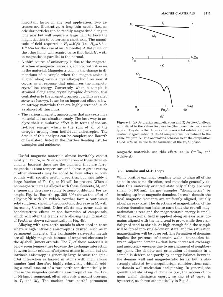
Useful magnetic materials almost inevitably consistmostly of Fe, Co, or Ni or a combination of these three el-ements, because these are the elements that are ferro-magnetic at room temperature and above. A great varietyof other elements may be added to form alloys or com-pounds with specific useful properties, but inevitably alarge fraction of Fe, Co, or Ni will be present. When anonmagnetic metal is alloyed with these elements, Ms andTc generally decrease rapidly because of dilution. For ex-ample, Fig. 4a (Bozorth, pp. 308–309) shows the effect ofalloying Ni with Cu (which together form a continuoussolid solution), showing the monotonic decrease in Ms withincreasing Cu content. Other effects may occur, such asbandstructure effects or the formation of compounds,which will alter the trends with alloying (e.g., formationof Fe3Al, as shown schematically in Fig. 4b).
Alloying with rare-earth metals is often used in caseswhere a high intrinsic anisotropy is desired, such as inpermanent magnets. The lanthanide rare-earth metalsare all highly magnetic because of unpaired electrons inthe 4f-shell (inner) orbitals. The Tc of these materials isbelow room temperature because the exchange interactionbetween inner orbitals of adjacent atoms is small, but theintrinsic anisotropy is generally large because the spin–orbit interaction is largest in atoms with high atomicnumber (and therefore highly relativistic orbitals). Add-ing a small amount of a rare earth can dramatically in-crease the magnetocrystalline anisotropy of an Fe-, Co-,or Ni-based compound, often with only a modest decreasein Tc and Ms. The modern ‘‘rare earth’’ permanent
magnetic materials use this effect, as in SmCo5 andNd2Fe14B.
3.5. Domains and M–H Loops
While positive exchange coupling tends to align all of thespins in the same direction, real materials generally ex-hibit this uniformly oriented state only if they are verysmall (o100 nm). Larger samples ‘‘demagnetize’’ bybreaking up into magnetic domains. In each domain thelocal magnetic moments are uniformly aligned, usuallyalong an easy axis. The directions of magnetization of thevarious domains can balance such that the overall mag-netization is zero and the magnetostatic energy is small.When an external field is applied along an easy axis, do-mains aligned with the field tend to grow, while those an-tialigned tend to shrink. At high enough field the samplewill be forced into single-domain state, and the saturationmagnetization will be observed. The formation of domainsimplies the presence of domain walls—boundaries be-tween adjacent domains—that have increased exchangeand anisotropy energies due to misalignment of neighbor-ing spins. The density and orientation of domains in asample is determined partly by energy balance betweenthe domain wall and magnetostatic terms, but is alsostrongly affected by nonequilibrium considerations suchas domain wall nucleation and pinning. In general, thegrowth and shrinking of domains (i.e., the motion of do-main walls) dissipates energy, so the M–H curve ishysteretic, as shown schematically in Fig. 5.
Ms
Ms
Ms
Tc Tc
00
0 Fe3Al0
40%Cu
40%Al
(a)
(b)
Figure 4. (a) Saturation magnetization and Tc for Fe–Cu alloys,normalized to the values for pure Fe (the monotonic decrease istypical of systems that form a continuous solid solution); (b) sat-uration magnetization of Fe–Al compositions, normalized to thevalue for pure Fe. The anomalous behavior near the compositionFe3Al (25% Al) is due to the formation of the Fe3Al phase.
MAGNETIC MATERIALS 2415

This hysteretic, sigmoidally shaped M–H curve is verytypical of ferromagnetic materials. Four important param-eters are immediately evident from examination of theM–H curve:
1. The limiting magnetization is just Ms, thesingle most important measure of a ferromagneticmaterial.
2. The slope of the M–H curve at M¼0 is the small-signal permeability m(0), which measures the re-sponsiveness of the magnetic material to an exter-nal field when it is close to its demagnetized state.This parameter is particularly important for softmagnetic materials, which use the magnetic mate-rial to obtain a flux multiplication by the factor m(0).This parameter is determined partly by the magnet-ic anisotropy that is characteristic of the materialbut is also affected by factors that impede domain-wall motion, such as physical grain structure, mi-croscopic inclusions, dislocations, or magnitude ofthe magnetocrystalline anisotropy.
3. The magnetization observed at zero field (after thesample has been fully magnetized) is called the re-manence, Mr. This is an important parameter forpermanent magnets, as it measures the magnitudeof M available when the material is isolated. Notethat the ‘‘squareness ratio,’’ Mr/Ms, is dominated byextrinsic aspects of the material, such as grainstructure and defect, along with underlying an-isotropies including the shape of the specimen.
4. The field required to reduce the external magneti-zation to zero (again, defined only after the samplehas first been fully magnetized) is called the ‘‘intrin-sic coercivity’’ or coercive field Hc. At this field, thesample is in a multidomain state and the magneti-zations from all of the various domains exactly can-cel out. The coercive field is an important propertyfor permanent magnets, as it measures the ability ofa material to withstand the action of an externalmagnetic field, whether applied or self-generated. It
is also determined mainly by extrinsic aspects of thematerial such as grain structure.
The interpretation of M–H loops can often involve sub-tle aspects of the loop, including directional properties, theapproach to saturation, possible nonsigmoidal curving,discrete jumps (known as ‘‘Barkhausen jumps’’), and soon. These may reflect coherent rotation of spins in a do-main when the external field is not aligned with an easyaxis or may be due to subtleties of domain wall motion.Development of superior magnetic materials often involvesintensive research into these issues, but usually the de-signers of devices need only focus on a few properties.
3.6. Negative Exchange Interaction
The exchange interaction, as mentioned previously, neednot be positive, inducing alignment of adjacent spins.When it is negative, adjacent spins will tend to align an-tiparallel. This can lead to a variety of behaviors depend-ing on the structure of the material.
3.7. Antiferromagnetism
The simplest configuration that can be obtained with anegative exchange energy is antiferromagnetism, in whichthe spins on adjacent sites in a unit cell cancel to give nonet magnetic moment. A simple example is NiO, whichforms in the rock salt (NaCl) structure (see Fig. 6). Theordering temperature for antiferromagnetic materials iscalled the ‘‘Neel temperature’’, TN, after the discoverer ofantiferromagnetism, and is analogous to the Curie tem-perature of a ferromagnet. Above TN¼ 2501C, NiO is ofcourse, paramagnetic. In the antiferromagnetic state thesusceptibility is not negative, as in the case of a diamagnet(which has no permanent dipoles) but is positive, small,and depends on the direction of the external field due tointrinsic magnetocrystalline anisotropy. The details of spinconfigurations and other properties of antiferromagnets
[010] [111]
[101]−
−
Figure 6. Antiferromagnetic structure of NiO, showing Ni atomsin the ð1 0 1Þ plane. The spins are aligned along ½1 1 1� directions asshown. The magnetic unit cell is twice the length of the crystal-lographic unit cell.
M
H
Hc
Mr
Ms
�(0)
Figure 5. Schematic M–H curve, showing saturation magneti-zation Ms, remanent magnetization Mr, coercive force Hc, and ini-tial permeability m(0) (defined for an initially demagnetizedsample, i.e., with H¼0 and M¼0).
2416 MAGNETIC MATERIALS

can be very complicated. Antiferromagnetism is difficult todetect by conventional magnetic measurements. Neutronscattering measurements are typically required to confirmthe existence of antiferromagnetism.
Antiferromagnetic materials have been known and un-derstood since the work of Neel beginning in 1932, butthere are presently no important applications of bulk an-tiferromagnetic materials. Thin films (B1–100 nm thick)of antiferromagnetic materials now play an important rolein state-of-the art magnetic recording, specifically in mag-netoresistive read heads. The antiferromagnetic thin filmsare used to magnetically bias the magnetoresistive sensorusing a phenomenon called exchange anisotrophy: thesurface interaction between a ferromagnetic and antifer-romagnetic material in intimate contact (see Fig. 7.). Sincethis is an interfacial phenomenon, its magnitude is onlysignificant when the surface/volume ratio is high, as in avery thin film.
3.8. Ferrimagnetism
In a compound with two magnetic sublattices and antifer-romagnetic coupling, the magnetic moments of each sub-lattice will generally not cancel exactly. Then the materialwill exhibit an overall magnetization that in many regardswill appear exactly like that of a ferromagnet, with ahysteretic M–H loop, a coercivity, and a remanence. Suchmaterials are called ferrimagnets, because the prototypi-cal examples are ferrites. Some properties, such as thetemperature dependence of the magnetization, can be rad-ically different from those of ferromagnets. For example,the different temperature dependencies of the magnetiza-tion on two sublattices can sometimes lead to exact can-cellation of the net magnetization at a particulartemperature, called the compensation temperature Tcomp
(often denoted Tc, which leads to confusion with the Curietemperature). At that temperature the material behavesas if it were an antiferromagnet.
While ferrimagnets behave in many ways like ferro-magnets, the highest saturation flux density in ferrimag-nets is typically only about 0.6 T, and they costsignificantly more than iron or silicon iron. Their crucialadvantage is that they are usually good insulators andtherefore are useful at high frequencies due to low eddy-current losses. Three classes of ferromagnetic materialsare predominant in applications:
* Garnets have a generic formula of R3Fe5O12, where Rrepresents a lanthanoid (Sc, Y, or lanthanide rareearth). These compounds have a Tc around 2751C anda rather low saturation flux density at room temper-ature, Bs¼ 0.18 T. They have proven useful for bubblememories because high-quality single-crystal garnetscan be prepared, and they continue to be used forUHF applications because they have particularly lowlosses in that frequency regime.
* Spinel ferrites are an especially large class of mate-rials with a wide range of properties. The generic for-mula unit is AB2O4, where A is a divalent ion and B isa trivalent ion, usually Fe3þ . Most of the usefulspinel ferrites are magnetically soft (that is, theyhave a low anisotropy energy and a high permeabil-ity). The prototypical spinel ferrite is Fe3O4, but Zn-substituted MnFe2O4 and NiFe2O4 are the soft fer-rites used in most applications. Another extremelyimportant ferrite is commonly used as a magnetic re-cording medium—namely, g—Fe2O3, which is a mod-ified spinel in which one in nine Fe sites issystematically vacant.
* Hexagonal ferrites are a much smaller class of ma-terials, but this class includes the important ceramicpermanent magnet materials. A typical formula unitfor a hard hexagonal ferrite is BaFe9O12. These ma-terials have a platelet-type growth habit with a veryhigh uniaxial anisotropy and an easy axis normal tothe platelet. This makes it difficult for the magneti-zation of a platelet to change, which accounts for thehard magnetic properties. The fact that these mate-rials are insulating is often not an important issuesince they are used to create a dc magnetic field.
When a magnetic dipole is aligned (e.g., by intrinsicanisotropy) along an axis and a radiofrequency (RF) fieldis applied perpendicular to that axis, the dipole does notrespond simply by oscillating in the direction of the RFfield, but it precesses around its axis in accordance withclassical mechanics. The precession frequency is common-ly expressed as o¼ gHan, where g is the gyromagnetic con-stant [g¼ 35 kHz/(A/m) for most materials] and Han is theanisotropy field. If the RF field is at exactly this frequency,the dipole can readily absorb energy from the field(and convert it into heat via coupling to the lattice). This
Ferromagneticlayer
Antiferromagneticlayer
Loop offsetin H
One stable stateat H = 0
H
M
Figure 7. Schematic illustration of exchangeanisotropy arising from interface coupling be-tween an antiferromagnetic and ferromagnet-ic material. The schematic M–H loop indicatesthat the loop is offset in H and that with noexternal field there is only one stable state(namely, the saturated state). That is, at H¼0there can be no domain structure.
MAGNETIC MATERIALS 2417

phenomenon is known as ferromagnetic resonance (FMR),although it is most important in insulating ferrimagnetswhere eddy currents do not already dominate the losses.Above the FMR frequency the magnetic material has anonmagnetic response.
At very high frequencies the response of ferrimagnets isnot dominated by domain-wall motion, which is sluggish,but by coherent rotation of the spins in the sample. Thenthe permeability is given simply by mc¼Bs/Han, so oFMR mc
¼ gBs. This equation, known as ‘‘Snoek’s law,’’ says that fora given material, a higher FMR frequency can only be ob-tained at the cost of a correspondingly smaller permeabil-ity. It is a basic limitation to the use of ferromagneticmaterials at frequencies above about 10 MHz. Other is-sues, such as domain-wall resonances, may reduce themaximum frequency even further.
3.9. Metamagnetism
If a large enough magnetic field is applied to an antifer-romagnet along an easy axis, the spins that are anti-aligned with the field will suddenly flip their orientation toachieve a lower energy state; that is, for a sufficiently highmagnetic field, H, the magnetostatic energy m �H (wherem is the dipole moment of an individual atom) will inev-itably outweigh the exchange energy. In some antiferro-magnetic materials this flipping can be observed withachievable magnetic fields; it is then called metamagne-tism. Note that in principle all antiferromagnets will ex-hibit this behavior at a high enough field—the distinctionis only in whether the required field can be produced inthe laboratory.
Antiferromagnets with a relatively low anisotropy en-ergy can exhibit an intermediate state between the anti-ferromagnetic and metamagnetic states as the field isincreased. In this case, application of the field along theeasy axis will cause the spins to reorient perpendicular tothe magnetic field, and still in an approximately antifer-romagnetic configuration, as shown schematically inFig. 8. This transition is called ‘‘spin flopping.’’
Neither metamagnetism nor the spin-flop transitionare of practical significance in bulk applications of mag-netism. However, the metamagnetic transition is an
essential feature of the phenomenon of giant magnetore-sistance (GMR), which is observed in metallic thin-filmferromagnet/paramagnet multilayers (vide infra).
3.10. Spin Glass State
When a magnetic material has structural disorder, it issometimes not possible for the exchange interactionamong various neighbors to be satisfied, and no long-range orientational order (either ferromagnetic or antifer-romagnetic) can be achieved. At low enough temperaturesuch a ‘‘frustrated’’ material will achieve a quasiorderedconfiguration in which the spins are static but aligned inrandom directions. This is the ‘‘spin glass’’ state. In a givensample, the magnetic properties are found to be historydependent: For example, the saturation magnetization de-pends on whether the sample was cooled in a magneticfield or in zero field. So-called spin glass materials shouldnot be confused with the metallic glasses discussed later.The nature of the spin glass state has been a productivearea of study for physicists for many years, but the phe-nomenon has no current engineering significance [6].
A related concept is that of ‘‘geometric frustration,’’which occurs in materials that have triangular site coor-dination and that therefore are frustrated even in a per-fectly ordered material. These materials are presentlybeing explored intensively by physicists, but also haveno current engineering significance [7].
3.11. Double-Exchange Materials
Along with the exchange mechanisms listed previously,there is a fourth mechanism, double exchange, that is rel-evant only to a small class of materials. The prototypematerial is (La,Ca)MnO3, a perovskite oxide, in which theCa substituted for La acts as an electron donor. Electronshopping from one Mn atom to another do not change theirspin orientation during the hop, so the Mn atoms orientferromagnetically. The most interesting property of thesematerials is observed in the paramagnetic state—in zerofield the Mn spins are randomly oriented, inhabiting elec-tron hopping and yielding a high resistivity. When the Mnspins are partially aligned by applying a large magneticfield, the hopping probability is enhanced, and the resist-ivity decreases dramatically. At an optimum temperature(near Tc), a resistivity decrease by a factor of 105 to 106 hasbeen observed at a field of 4 MA/m, a result that has ledthe effect to be known as colossal magnetoresistance(CMR). The effect is colossal at low temperatures and foronly a small temperature range, and it requires very largefields to be applied, so it has not proven useful for engi-neering applications at present.
3.12. Superparamagnetism
In small single-domain particles of ferromagnetic materi-al, the magnetization tends to align along the easy axis,and the energy barrier required to move the magnetiza-tion is on the order of KV, where K is the anisotropy energydensity and V is the volume of the particle. For the simplecase of uniaxial anisotropy, DE¼KV. If the thermal energykBT is greater than this energy, then fluctuations in the
Direction of applied field:
Ground state Spin-floptransition
Metamagnetictransition
H = 0 H = highH = moderateK = low
Figure 8. The spin-flop transition and metamagnetic transitionin antiferromagnetic materials. The spin-flop transition occursonly in materials with relatively low magnetic anisotropy energyK, binding the spins to the easy axis (in the case, the horizontalaxis).
2418 MAGNETIC MATERIALS

orientation of the magnetization will lead to zero sponta-neous magnetization and a response to an applied fieldthat is analogous to the local moments of a normal para-magnetic material. The effect is seen, for example, in Coparticles smaller than about 7.5 nm. The moment of a Cosphere of diameter 7.5 nm is roughly 20,000 times largerthan the moment of single Co atom, so the effect is calledsuperparamagnetism. While superparamagnetism is nottechnologically useful itself, it does represent an impor-tant limitation to the particle size of future magnetic re-cording media, and is therefore being intensivelyinvestigated.
3.13. Thin Films
Thin films of magnetic materials behave exactly like bulkmagnetic materials in most respects, albeit in profoundlydifferent regimes for some parameters. For example, thinfilms have a demagnetization factor normal to the film andessentially zero demagnetization factor in the plane of thefilm. Thus it is generally very hard to magnetize a thinfilm normal to the plane but fairly easy to move the mag-netization in the plane. A simple consideration such asthis can have wide-ranging implications, from an in-creased FMR frequency to gross effects on the structureof domain walls (i.e., the transition from conventionalBloch walls to Neel walls as the film thickness is de-creased below about 100 nm). Thin films also tend to havestresses that are extremely high compared to stresses inbulk materials—500 MPa values are not uncommon.These stresses couple to the magnetostriction of the ma-terial to create a stress anisotropy that can strongly in-fluence the magnetic behavior.
Thin films are used in a wide variety of applications,the most important of which are as media in hard disksand magnetooptic disks, miniature electromagnets inhard-disk write heads, and magnetoresistive sensors inhard-disk read heads.
Thin films inherently possess a unique direction, thegrowth direction. This is usually the normal, although itcan be oblique if the incident atomic flux used to grow thefilm arrives from an oblique angle. For some materials thegrowth direction directly leads to a large intrinsic uniaxialanisotropy. For example, in amorphous Tb–Fe one mightexpect that there would be no anisotropy at all. Instead,films grown with the incident Tb and Fe atoms arrivingessentially perpendicular to the substrate exhibit a largeintrinsic uniaxial anisotropy oriented along the normal,and with a sense that leads to a perpendicular easy axis.The anisotropy is sufficient to overcome demagnetization,so domains form in which the magnetization is orientedperpendicular to the film. Such materials are used inmagnetooptic recording (vide infra) [8].
Some behaviors seen in thin films are either absent ornot commonly observed in bulk magnetic materials. Animportant example is the phenomenon of so-called giantmagnetoresistance in thin-film multilayers. These multi-layers are typically formed by sequentially depositingmetallic ferromagnetic and paramagnetic layers, eachB1–3 nm thick, using sputtering or evaporation ina high-vacuum chamber. Between two and a hundred
layers might be built up in this way. The ferromagneticlayers couple with each other by the RKKY interactionthrough the paramagnetic metal, so, depending on thethickness of the paramagnetic layer, the interlayer cou-pling may be antiferromagnetic or ferromagnetic. For ex-ample, a film consisting of 100 repeats of 1.0-nm-thick Coadjacent to 0.6–nm-thick Cu exhibits an antiferromagnet-ic state at zero field; even though each Co layer is indi-vidually ferromagnetic, alternate layers have oppositelydirected magnetizations. When a moderate field H is ap-plied, the magnetizations of all of the layers align with theexternal field, producing a metamagnetic transition.
Baibich et al. [9] discovered the most interesting aspectof the metamagnetic transition in metallic multilayers:the effect it has on the resistivity of the sample. Thealigned state has a greatly reduced resistivity comparedto the antialigned state. The magnetoresistance ratio [R(H¼ 0)—R(H¼Hs)]/R(H¼Hs) can be as high as B100% de-pending on the choice of materials. This is far greater thanthe highest normal magnetoresistance observed in anymaterial at room temperature; hence the name giant mag-netoresistance. It is attributed to spin-dependent scatter-ing of electrons, which is enhanced when magnetizationsof adjacent layers are antialigned. This effect is crucial forthe highest-performance magnetic disk read heads beingcurrently designed (vide infra) [10].
4. MAGNETIC MATERIALS USED IN APPLICATIONS
Useful magnetic materials are often divided into threecategories:
* Soft magnets, in which the magnetization is readilychanged with an external field, thereby providing aflux-multiplying effect
* Hard magnets (permanent magnets), which havehigh coercive fields and therefore resist demagneti-zation by stray fields including their own
* Magnet recording media, which combine aspects ofsoftness and hardness
4.1. Soft Magnetic Materials
Soft magnetic materials are used in applications such astransformers and inductors. An obvious example would bethe iron, known as ‘‘electrical steel,’’ used in transformersfor inexpensive power supplies. At frequencies aboveabout 10 kHz, eddy currents limit the use of metallic mag-netic materials, so high-resistivity ferrites such as (Mn,Zn)Fe2O4 are used.
4.1.1. Permeability. An important property of soft mag-netic materials is their relative permeability, nominallydefined by mr¼B/m0H. Actually, since the B(H) curve isneither linear nor single-valued, a large number of usefulpermeability parameters can be defined, such as the ini-tial permeability, the maximum permeability, and the an-hysteretic permeability. For simplicity, we will consideronly the initial small-signal permeability, defined asmð0Þ � @B=@H
�
�
H¼ 0. Values from m(0)¼10 (high-frequency
MAGNETIC MATERIALS 2419

ferrites) to m(0)¼ 10,000 (low-frequency inductors) aretypically encountered in applications.
4.1.2. Power Devices. Probably the main use of mag-netic materials at present, on a weight basis, is in powertransformers. These can range from huge transformersused in substations, to miniature transformers used toconvert line voltage to a level suitable for small consumerdevices, to small ferrite transformers used in switchingpower supplies.
Low-frequency power applications almost inevitablyemploy low Si percentage Fe–Si alloys known as ‘‘siliconiron’’ or ‘‘electrical steel.’’ This is because Fe is by far thecheapest magnetic material available. The coercive field ofpure Fe is typically about 80 A/m. The addition of a smallamount of Si to Fe lowers the anisotropy, resulting in low-er losses and a coercive force of about 40 A/m. It also sub-stantially increases the resistivity, which decreases eddycurrents. Eddy currents in transformers are usually fur-ther reduced by lamination (i.e., using a stack of Fe–Siplates, each electrically insulated by a coating layer, rath-er than a single thick piece). The laminations are ar-ranged so that eddy currents are interrupted by thepresence of the insulator and forced to circulate only with-in each lamination (i.e., so that any AC magnetic flux isperpendicular to the normal). Properly designed, thethickness of each plate should be smaller than a skindepth d, given by d¼ (2r/om)1/2, where r is resistivity, o isthe angular frequency of the AC magnetic field, and m isthe permeability. Note that the permeability can also befrequency-dependent.
Improved varieties of silicon iron are prepared usingspecific sequences of forging (rolling) and annealing to ob-tain a grain-oriented microstructure. In such materialsthe crystallographic orientation of individual grains isforced to be aligned over the entire piece. The advantageis that materials with lower losses are obtained, althoughthe material is also somewhat more expensive. At present,most power transformers utilize grain-oriented siliconiron.
The highest-performance materials for low-frequencytransformer applications are the metallic glasses, amor-phous alloys of Fe and Co with one or more metalloid ad-ditions (usually B, C, Si, and P). These materials can havelosses that are 10 times smaller than silicon iron and co-ercive fields below 0.5 A/m. But the saturation flux densityis generally B1.5 T, and the materials are substantiallymore expensive than silicon iron. These negative aspectsof metallic glasses have precluded their widespread use.
Power supplies with low weight and volume are highlydesirable for some electronic applications, and this can beachieved with the design called ‘‘switching’’ power sup-plies. An additional benefit is circuit versatility and flex-ibility, while the main tradeoffs are increased cost anddesign complexity. A switching power supply uses powerelectronics [typically metal oxide semiconductor field-ef-fect transistors (MOSFETs)] to chop and rectify power athigh frequency, a power transformer or inductor to changethe voltage, and control electronics to synchronize andcontrol the system. The frequencies used range from about50 kHz to a present upper limit of 1 MHz.
At these frequencies, metallic ferromagnets cannot beused as the desirable lamination thickness would be pro-hibitively small. Fortunately at such high frequencies, theenergy that must be stored in the transformer or inductoris correspondingly small for a given power capacity (EBP/o, where E is the maximum stored energy, P is the max-imum power, and o is the angular frequency). Therefore,the cost of the magnetic part need not dominate, especiallyconsidering the cost of the electronics involved, so the useof relatively expensive but very high resistivity ferrites isfeasible. In most cases an (Mn,Zn)Fe2O4 spinel ferrite ischosen as a compromise between saturation flux density,losses, resistivity, and cost. At the highest frequencies,(Ni,Zn)Fe2O4 may prove useful, as it has a higher resist-ivity and therefore is less susceptible to eddy-currentlosses.
Motors and generators inevitably employ iron or siliconiron to act as a flux concentrator. The armature and statorare commonly constructed of grain-oriented silicon iron,although small motors often employ nonoriented siliconiron or metallic glass materials. As in transformers, theferromagnetic parts must be laminated to reduce eddy-current losses.
4.1.3. Inductors. Small-signal transformers and induc-tors are used in a variety of circuit applications, as in im-pedance-matching and isolation transformers, antennas,and chokes. Signal-level devices do not have to carry sub-stantial power, so they can be small and the cost of mate-rials can easily be outweighed by performanceconsiderations. Thus a wider variety of magnetic materi-als is used in these devices.
At audiofrequencies and below, transformers and in-ductors were once commonly used for signal applications.For example, long-distance analog telephone circuits werebalanced by the periodic addition of loading coils—induc-tors designed to match the large distributed capacitance ofphonelines. A common choice for the magnetic core inthose coils was Permalloy (Ni80Fe20) or a related alloy, andthe cores were formed by rolling a long tape into a toroidalcore. However, in modern telecommunication systems theanalog signals are quickly converted to digital signals atthe central exchange and then transmitted by the fiber-optic, satellite, or microwave relay. The need for loadingcoils is minimal. Similarly, the function of audiofrequencyimpedance-matching transformers and other inductiveelectronic components has largely been displaced bymore elaborate but much cheaper integrated circuit de-signs. Low-frequency magnetics are used in modem isola-tion transformers to provide DC electrical isolation withaudio coupling; these are made with either laminated me-tallic or solid ferrite cores.
At RF frequencies (50 kHz–50 MHz) magnetic cores arewidely used; for example, in antennas, RF transformers,chokes, and resonant circuits. The usual choices for mag-netic cores are the spinels (Mn,Zn)Fe2O4 (up to about1 MHz) and (Ni,Zn)Fe2O4 (up to about 10–50 MHz). Themanganese zinc ferrites are cheaper but have a resistivitytypically less than 1000O � cm. Eddy current losses limittheir usefulness at high frequencies. The initial perme-ability is roughly 1000–3000. Nickel zinc ferrites can have
2420 MAGNETIC MATERIALS

resistivities as high as 105O � cm and initial permeabilitieson the order of 1000. Their upper frequency limit is dic-tated by the need to avoid FMR losses. Material designedfor operation above about 10 MHz typically is preparedwith moderate porosity to inhibit domain-wall motion andlosses associated with domain-wall resonance. The perme-ability mechanism then is limited to that of coherent ro-tation of the spins, which implies a much smaller value(mcBMs/HkB10–100).
Above about 50 MHz, magnetic materials are not com-monly used in transformers and inductors, as Snoek’s lawdemands that the permeability be uselessly small in orderfor the FMR frequency to be sufficiently greater than thefrequency of operation. Snoek’s law can be circumventedby the use of materials with a large biaxial anisotropy(e.g., the hexagonal magentoplumbite-type ferrites) or byusing thin films with a high saturation magnetization. Atpresent, however, those approaches are not commerciallyimportant.
4.1.4. Write Heads. An important application of softmagnetic materials is in the recording heads used intape and disk systems. Write heads essentially consist ofan electromagnet with a toroidal magnetic core and a verysmall airgap (B100 nm to 300 nm). The flux that extendsfrom the airgap, called the ‘‘fringing field,’’ is used to mag-netize the magnetic medium passing nearby (see Fig. 9).In tape and floppy-disk systems the magnetic medium isin actual contact with the head, while in hard-disk sys-tems the head flies aerodynamically over the spinningmedium at a height of 25–75 nm. The maximum magneticfield available for magnetizing the medium is proportionalto the saturation magnetization of the head material.
Originally the magnetic recording heads were madefrom laminated metal alloys, such as Permalloy or Sen-dust (an alloy of Fe, Si, and Al notable for being magnet-ically soft and physically very hard), but as recording
densities and frequencies increased, an inevitable movewas made to ferrite materials. Ferrite heads are madefrom cast pieces that are carefully polished to form a pre-cise airgap and then are assembled with the driving coil.As recording densities have increased, media with highercoercivities are necessary, so head materials with highsaturation magnetization are needed. Unfortunately thisis where the ferrites are most deficient, with maximumBsB0.6 T. One approach to obtain improved performanceis to add a thin film of relatively high Bs material (such asPermalloy, Bs¼ 0.9–1.1 T) on the inside edge of the gap ofeach piece. The thin film acts as a flux concentrator andincreases the fringing field significantly. This approach iscalled the metal-in-gap (MIG) design.
The highest-performance recording heads are con-structed using thin films and photolithography. Theyhave the advantage of great precision in layout, leadingto extremely narrow pole tips, precise gap widths, andprecise placement of the driving coils. Permalloy and re-lated alloys are most commonly used at present, but softamorphous alloys such as Co0.85Nb0.08Zr0.7 offer signifi-cant improvements with BsB50% greater than Permalloy.The resistivity of the amorphous alloys is in the rangerB100mO � cm, about fivefold higher than Permalloy,which reduces eddy-current losses, allowing recording athigher frequencies. Further advantage can be obtained byusing the recently developed nanocrystalline (grain sizeB1–5 nm) alloys such as Fe0.92Ta0.05N0.03, which have ex-tremely high BsB2.0 T and also have resistivities in therange of 100–150mO � cm. These materials are being vig-orously developed for future generations of high-perfor-mance recording, especially hard-disk drives.
4.1.5. Read Heads. The same magnetic structure thatis used for magnetic recording can also be used for readingthe recorded signal. The passage of recorded domainsacross the gap of the recording head will induce a smallvoltage on the driving coil, which is amplified and pro-cessed. Indeed, this inductive read head is the simplestand cheapest approach to magnetic recording. However,the signal level is very low and limits the performance ofhard-disk drives. The present generation of hard diskdrives uses a separate magnetic structure (incorporatedin a single read/write head) for reading the recorded mag-netic signal. The sensor in this device is a magnetoresis-tive thin film made of Permalloy and biased with a DCcurrent. External flux from the recording medium couplesto the Permalloy film, rotating the magnetization with re-spect to the fixed direction of the DC current. This changesthe resistance of the Permalloy [the so-called conventionalor anisotropic magnetoresistance effect (AMR)] and there-fore the voltage developed across the device. The AMR ef-fect is relatively small, about 5%, but is sufficient todeliver signal superior to that of an inductive head.
Superior performance can be obtained by incorporatingmaterials that exhibit giant magnetoresistance. These canhave responses that are about 10-fold higher than AMRmaterials. So-called spin valves employ the same physicalprinciple as GMR (namely, spin-dependent scattering) in amore highly controlled and responsive magnetic structure.The higher signal output of spin valve read heads, in
Signal
Direction of tape or disk motion
Figure 9. Schematic of a magnetic recording head. Recording isaccomplished using the magnetic fringing field (i.e., the field thatleaks from the gap).
MAGNETIC MATERIALS 2421

conjunction with careful redesign of the entire magneticrecording system (including media, head structure, elec-tronics, signal processing, etc.), can lead to substantial in-crease in recording density.
4.1.6. Shields. Soft magnetic materials are also used tomake magnetic shields, typically used to protect electroniccomponents from magnetic interference or to contain theexternal field around a component that generates mag-netic flux. An example of the former are shields for cath-ode-ray tubes, such as computer monitors, while anexample of the latter are shields for speakers, such as‘‘multimedia’’ speakers intended for placement close to a(unshielded) monitor. These shields are usually formedfrom Permalloy and related alloys. Often ‘‘Mumetal’’ isspecified for these applications—this originally designateda particular Fe–Ni–Cu alloy but it is now used genericallyto refer to many high-permeability alloys. Note that RFshields (unlike DC magnetic shields) rely on eddy currentscreening and use high-conductivity paramagnetic metalssuch as Cu.
A related application is the use of materials that absorbRF energy. These are typically lossy ferrites and are usedin the form of beads threaded on wires, where it is desiredto suppress high-frequency signals. Manganese–zinc fer-rites are generally used for this purpose, although nickel–zinc is used to obtain the highest cutoff frequencies. Lossyferrites can also be used as an antiradar coating on mil-itary aircraft.
4.2. Hard (Permanent) Magnets
Permanent magnets are used in a wide variety of appli-cations where a static magnetic field is desired. The dom-inant uses are in speakers and DC motors and as holdingmagnets. The field available from a given permanent mag-net depends on the physical configuration but is limited toBs, the saturation flux density in the optimum case. Spe-cifically, for a toroidal part with a small airgap (seeFig. 10), the flux density in the gap will be Bs. For Fethis is Bs¼ 2.15 T, while for Fe0.6Co0.4 it is Bs¼ 2.43 T [11,p. 190], the highest value for any known bulk material. In
less optimum geometries, the available flux density can begreatly reduced, as determined by magnetostatics. For ar-bitrary-shaped parts, the usual approach is to employ fi-nite-element numerical calculations to infer the fluxdistribution.
In general, where the design figure of merit is the fluxavailable per unit volume of magnetic material, the cor-responding figure of merit for the magnetic material is theenergy product (BH)max [i.e., the largest value measuredat any point in the second quadrant (positive B, negativeH) of the B–H curve]. This is only a crude way to evaluatethe usefulness of a material; nevertheless it is indicativeand is commonly quoted by permanent magnet manufac-turers. Four main types of permanent magnet materialsare commonly used:
* Alnico, a class of Fe–Al–Ni–Co–Cu alloys. The prop-erties of this material are entirely dependent on com-plex metallurgical processing and microstructuralcontrol. Commonly used Alinco materials have(BH)max¼ 50� 103 J/m3.
* Barium ferrite, typically BaO � (Fe2O3)6, is the stan-dard ‘‘ceramic’’ magnetic material. The typical value(BH)max¼ 25� 103 J/m3 is smaller than that of Alni-co, but the material is both lower density and cheaperto produce than Alnico and has almost entirely re-placed Alnico in highly cost-sensitive applications.The high value of (BH)max in this and the followingmaterials is due to the very high intrinsic anisotropy.
* Sm–Co is the standard high-performance ‘‘rare earth’’permanent magnet, with (BH)max¼ 160� 103 J/m3.The major disadvantage of this material is its cost.
* Nd–Fe–B, a more recent material, has an even highervalue for (BH)max¼ 320� 103 J/m3 than Sm–Co, andit value is less expensive. The major disadvantage ofthis material in some applications is that the Tc issomewhat low, TcB1501C.
Loudspeakers have long been a dominant applicationfor permanent magnetic materials. The permanent mag-net is used to establish a magnetic field in an annular re-gion in which the voice coil is mounted. When a current isdriven through the voice coil, an axial force is produced, inaccordance with the Lorentz relation, F¼ ev�B, where Fis the force on an electron, e is the charge on an electron,and v is the velocity of the electron. Motion of the voice coilis coupled to a speaker cone to move the air efficiently andthereby produce sound waves.
The energy product of a magnetic material is a goodfigure of merit for speaker applications, since for a givendesign, a higher-energy product will result in a higher fluxdensity in the annular gap. Most loudspeakers are low-priced components, so the cost of the magnetic material isthe other key factor. For this reason, barium ferrite is thedominant material used. In some applications, such ashigh-performance earphones, the amount of magnetic ma-terial is small so materials cost is less critical. In the past,Sm–Co magnets have been used for these applications,though Nd–Fe–B magnets are now clearly the best overallchoice.
Yoke
Air gap
Permanentmagnet
Figure 10. Airgap in magnetic circuits. The gray regions repre-sent permanent magnet material, with the direction of magneti-zation shown. The hatched region represents soft magneticmaterial, which is used to complete the magnetic circuit.
2422 MAGNETIC MATERIALS

The materials used for permanent magnets inevitablycost more than silicon iron, so large motors and generatorsalways use soft magnetic materials wound with coils tocreate the required magnetic field. In small motors, theeconomics are dominated by the cost of fabrication; thesmall coils and fine tolerances needed for electromagnetmotors outweigh the added cost of permanent magneticmaterials. A vast number of small DC motors are producedfor a very wide range of applications, from clock motors tothe dozens of motors in modern automobiles used to drivewindows, locks, seats, windshield wipers, and so on.
An economically important use of permanent magnetsis in the low-tech application of holding magnets. Theserange from decorative magnets for holding notes to a re-frigerator door to functional magnets for holding and seal-ing the refrigerator door shut to strong magnetic chucksfor holding ferrous materials for machine-forming opera-tions. In almost all cases cost is paramount, and bariumferrite is used. For some applications the ferrite powder ismixed with a polymer precursor, formed into a tape, andpolymerized to form a flexible magnet, albeit with reducednet flux density and therefore reduced holding power.
4.3. Magnetic Recording Media—Intermediate between Softand Hard
Magnetic recording is a huge business, dominated by thehard disks and floppy disks pervasive in personal comput-ers and by tape recording—audio, video, instrumentation,digital data storage, and so on. The media used in record-ing are magnetic materials that must have a relativelyhigh coercive force so that they do not spontaneously de-magnetize and lose information. But the coercive forcecannot be much greater than about 100 kA/m because theleakage flux from the recording head is limited and mustnevertheless be sufficient to saturate the medium.
The standard material used in tape and floppy-diskmedia is gamma iron oxide, g–Fe2O3. It is moderately ex-pensive to prepare (compared to conventional ferrites) be-cause extremely reproducible and controllable propertiesare required. Acicular (needle-shaped) particles B50 nmin diameter are prepared in order to obtain good recordingcharacteristics. The coercivity of most tapes is about 20–30 kA/m. More recent high-performance formulations usecobalt-modified g-Fe2O3, which has a thin cobalt-rich re-gion on the surface of the particles. This material has anincreased coercivity of about 50 kA/m and is routinelyused for videotape. In the past, CrO2 was used as ahigh-performance medium because it has a higher Ms
than g-Fe2O3 and can be prepared with a coercivity ashigh as 80 kA/m. However, it has a low Tc (only 1301C) andis relatively expensive, so it has been displaced by cobalt-modified g-Fe2O3.
Hard disks used in digital recording are aluminumplatters coated with paramagnetic Ni–P or Cr and thena recording medium such as Co–Cr. An extremely thinlayer of C is usually then deposited along with an evensmaller amount of lubricating fluid, in order to avoid cat-astrophic head contact with the medium (‘‘head crashes’’).The coercivity of hard-disk media is in the range
60–100 kA/m, and the saturation magnetization is about1000 kA/m.
For many years it was expected that magnetic bubblememory might find a role for data storage in computers.However, bubble memory is slow and expensive comparedto hard disks and semiconductor random-access memory(RAM). Its only advantages are that it is mechanicallymore robust than a hard-disk system, and it is more ra-diation resistant than semiconductor RAM. Therefore, theonly present use for bubble memory is in certain militaryapplications.
Bubble memories store data in cylindrical domains,perpendicular to the surface, that are generated in liq-uid-phase epitaxy (LPE) grown garnet films. The films aredesigned to have a large uniaxial anisotropy perpendicu-lar to the film plane and are chosen to meet a number ofother criteria. The bubbles are moved around using arotating external magnetic field created by a miniatureelectromagnet, and they are detected using a magnetore-sistance bridge.
Finally, there is magnetooptic recording. In this schemedata are stored on a plastic disk coated with an amorphousmetallic thin film such as Tb0.2Fe0.8 or similar composi-tions doped with Dy and Co. They have a large uniaxialanisotropy, with an easy axis perpendicular to the plane ofthe film, so as with the garnet films designed for magneticbubble applications, cylindrical domains are stable. Dataare written by focusing a laser on the desired spot, whichheats the films above its Tc, B100–1501C. If the film isexposed to a moderate magnetic field while it cools, theheated region will magnetize in the direction of the ap-plied field. Thus alternating regions of, say, north-up andsouth-up can be written. The data are read with the samelaser at lower power to avoid heating, using a polarizer todetect Faraday rotation (i.e., rotation of the polarization oflight when it interacts with a magnetic material). This ef-fect is known as Kerr rotation when it occurs on reflectionfrom a metallic magnetic surface. The Kerr rotation in amagnetic material is in the opposite sense for regionsmagnetized north-up versus south-up. The maximumKerr rotation in Tb–Fe films is rather small, B0.21, whichgives a low signal/noise ratio and correspondingly lowdata rate.
The data density in magnetooptic recording is compa-rable to that of a conventional CD-ROM but has the greatadvantage of being endlessly rewriteable. Magnetoopticdrives are slower for writing data and more expensivethan conventional hard drives, but they confer the advan-tage of cheap removable media and good archiveabilityand have found a small but significant market niche.
4.4. Miscellaneous
Along with the three conventional classes of applicationsfor magnetic materials, there are a wide variety of spe-cialized applications, too numerous to list exhaustively.
4.4.1. Nonreciprocal Materials. Some of the most inter-esting magnetic devices are based on the nonreciprocalpropagation of UHF signals in insulating magnetic
MAGNETIC MATERIALS 2423

materials. The behavior is formally identical to the smalloptical Faraday rotation observed in some nonferromag-netic materials, but the effect in ferrites can be very largeand is commonly used in microwave applications (e.g., inisolators and circulators).
The nonreciprocal phenomena are due to interaction ofthe incident radiation with the precessing electron spin(-see Magnetic resonance). A particularly straightforwardcase arises when the incident microwaves are circularlypolarized with a propagation vector parallel to the easyaxis of the magnetic material and at a frequency equal tothe natural precession frequency of the electron spins.Then, if the sense of the circular polarization is the sameas that of the electron spin precession, energy is readilytransferred to the spins and dissipated as loss. If the senseis opposite (corresponding to propagation in the oppositedirection), then there is little interaction and the loss isminimized. It is easy to imagine an isolator based on thedirectionality of this phenomenon, although the practicaldesign of this and other nonreciprocal microwave devicescan be very complex. In general, a moderately large ex-ternal biasing magnet is required to set the FMR frequen-cy equal to the operating frequency (a larger field isrequired for a higher operating frequency).
Three classes of materials dominate the magnetic ma-terials used for microwave applications—the figure ofmerit for microwave devices is usually proportional to1/DH, where DH is the FMR linewidth:
1. The garnet structure ferrites exhibit the highestperformance available because they have the lowestFMR linewidths. A typical value for polycrystallineceramic yttrium iron garnet (YIG) is DH¼4000 A/m.Single crystals with linewidths as low as 40 A/mhave been reported. Single crystals are relativelyexpensive but are usually the bets choice at low fre-quencies.
2. The spinel ferrites are useful in a number of cases.Nickel zinc ferrite is particularly useful at high pow-ers because it has a higher Tc than garnets, and it isoften used in the range above 10 GHz. Manganese–magnesium ferrites are used in the range of 5–10 GHz because their lower saturation magnetiza-tion allows biasing at lower field.
3. The Z-type hexagonal ferrites have a hard axis nor-mal to the basal plane, so the need for external bi-asing is reduced. They require expensive processingto produce oriented, high-quality ceramics. They aremost useful for mm-wave applications.
In general, the key issues in developing materials formicrowave applications are related to processing and mi-cro-structure control rather than exploring new composi-tions. Small grain size is important to minimize lossesform domain-wall resonance, to maximize the resistivity,and to make stronger materials that resist the thermalstresses caused by high-power operation. Obtaining a highdensity is always important, but densification usually isaccompanied by grain growth. The art of designing or
choosing a microwave magnetic material is in balancingthese conflicting requirements.
4.4.2. Ferrofluids. Ferrofluids are liquid suspensions ofmagnetic particles coated to avoid agglomeration. Typi-cally the liquid is a hydrocarbon or silicon, and the mag-netic particles are ferrites, but a wide range ofcombinations is possible. The behavior of ferrofluids isunique and scientifically interesting, and ferrofluids arecommercially used for such diverse applications as gas-tight seals for rotary shafts, heat transfer agents for loud-speaker voice coils, and damping systems.
BIBLIOGRAPHY
1. Plato, in The Dialogs of Plato, transl. B. Jowett, Great Books
of the Western World, Vol. 7, Benton, Chicago, 1952, p. 144.
2. W. Gilbert, De Magnete, transl. P. F. Mottelay, Dover, Mineola,NY, 1958.
3. J. D. Jackson, Classical Electrodynamics, Wiley, New York;
1962.
4. R. L. Carlin, Magnetochemistry, Springer-Verlag, Berlin,1986, p. 3.
5. E. H. Brandt, Science 243:349–355 (1989); Physics World
10(4):23–24 (1997).
6. K. Binder and A. P. Young, Spin glasses: Experimental facts,theoretical concepts, and open questions, Rev. Mod. Phys.58:801–976 (1986).
7. A. P. Ramirez, Ann. Rev. Mater. Sci. 24:453–480 (1994).
8. R. B. van Dover et al., Intrinsic anisotropy of Tb—Fe filmsprepared by magnetron co-sputtering, J. Appl. Phys. 57:3897–3899 (1985).
9. M. N. Baibich et al., Phys. Rev. Lett. 61:2472–2475 (1988).
10. S. S. P. Parkin, Giant magnetoresistance in magnetic nano-structures, Ann. Rev. Mater. Sci. 25:357–388 (1995).
11. R. M. Bozorth, Ferromagnetism, Van Nostrand, New York,1951.
FURTHER READING
R. M. Bozorth, Ferromagnetism, Van Nostrand, New York, 1951.
F. N. Bradley, Materials for Magnetic Functions, Hayden, NewYork, 1971.
F. Brailsford, Physical Principles of Magnetism, Van Nostrand,New York, 1966.
P. Campbell, Permanent Magnetic Materials and Their Applica-
tions, Cambridge Univ. Press, Cambridge, UK, 1994.
C. W. Chen, Soft Magnetic Materials, North Holland, Amsterdam,1977; reprinted by Dover, New York, 1986.
S. Chikazumi and S. H. Charap, Physics of Magnetism, Krieger,Malabar, FL, 1964.
B. D. Cullity, Introduction to Magnetic Materials, Addison-Wesley,Reading, MA, 1972.
D. Jiles, Introduction to Magnetic Materials, Chapman & Hall,London, 1991.
M. M. Schieber, Experimental Magnetochemistry, Wiley, NewYork, 1967.
J. Smit, H. P. J. Wijn, Ferrites, Wiley, New York, 1959.
2424 MAGNETIC MATERIALS

MAGNETIC MICROWAVE DEVICES
HOTON HOW
Hotech, Inc.Belmont, Massachusetts
In this article we discuss the following topics on magneticmicrowave devices: ferrite junction devices, lumped-ele-ment circulators, nonreciprocal resonators, YIG film de-vices, MSW devices, magnetooptic devices, absorbing/antireflection layers, and nonlinear responses. The articleis organized as follows: Section 1 presents a general the-oretical background underlying the physics for the oper-ation of ferrite components in microwave devices.Discussions include derivation of the Polder permeabilitytensor, the effective fields associated with electron spinmotion, the general dispersion spectrum and plane-wavesolutions for electromagnetic waves propagating in a bulkmagnetic medium, magnetostatic waves (MSWs) admittedby the geometry of a yttrium iron garnet (YIG) film, andthe nonlinear instabilities for spin waves occurring at highpower, including their routes leading to chaos. Section 2introduces ferrite junction devices, including circulatorsand isolators. Broadband operation, size reduction, power-handling issues, and other novel applications are dis-cussed in this section. Section 3 delineates the operationof lumped-element circulators in which interport imped-ances are portrayed. Section 4 defines the effective fieldassociated with a magnetic easy plane from an operationperspective. Section 5 gives an example that ferrite non-reciprocal resonator can be used as a phase shifter whoseoperation is independent of the derived phase shift angles.Section 6 describes YIG film devices incorporating mag-netostatic waves (MSWs), including delay lines, filters, di-rectional couplers, and resonators. Section 7 depictsnonlinear magnetic devices of frequency-selective powerlimiters, signal-to-noise enhancers, amplitude correctors,and ferrimagnetic echoing devices. Section 8 introducesmagnetic solitons, including Bloch domain wall solitionsand Microwave magnetic envelope solitons. Section 9 dis-cusses magnetooptic Kerr and Faraday effects, and theoperation of magnetooptic Bragg diffraction devices. Fi-nally, design of microwave absorbing layers and antire-flection layers is briefly mentioned in Section 10.
1. THEORETICAL BACKGROUND
This section provides a theoretical background underlyingthe physics that allows for the operation of a magneticmicrowave device. A magnetic microwave device generallyrequires the use of an insulating magnetic ferrite materialso that magnetization or spin motion is coupled to Max-well equations without inducing much eddy-current lossat high frequencies. Also, in order to eliminate domainwall motion, single-domain operation is demanded at RFfrequencies, and the ferrite material needs to be magne-tized to saturation using an external DC magnetic field.Alternatively, effective fields arising from either the crys-talline or shape anisotropy of the ferrite material may beused to fulfill the bias requirement of the magnetic device.
Thus, under small-signal approximations the electromag-netic property of the ferrite is described by a tensor per-meability whose nonzero off-diagonal elements permitnoble applications of nonreciprocal devices, for example.Most importantly, the permeability tensor can be variedby adjusting the bias field strength, resulting in tunabilityof the microwave device over frequencies.
A magnetic microwave device is normally operationalin the frequency range from 0.1 to 40 GHz or higher, andits performance can be interpreted in terms of the spin/magnetization motion of the ferrite material where cou-pling to optical/photon modes, elastic/phonon modes, orexchange/magnon modes may be utilized. Depending onthe regime of applications, a microwave magnetic devicemay be distinguished either as a retarded-wave device or amagnetostatic-wave device. The first class of devices in-cludes circulators, isolators, filters, phase shifters, patchantennas, and so on, whose operation requires the mag-netization vector to be coupled with the full set of Maxwellequations. The second class consists of mainly high-qual-ity single-crystal YIG film devices where the propagationof magnetization waves involves a wavelength comparableto the film thickness. As such, the displacement currentscan be omitted in Maxwell equations. This renders the so-called magnetostatic approximation, which implies thatthe resultant RF magnetic field can be derived from a sca-lar potential. Important magnetostatic devices include de-lay lines, filters, resonators, echo lines, and othernonlinear devices, whose operation complements theirlow-frequency counterparts below 2 GHz involving surfaceacoustic wave (SAW) devices.
In the following subsections we first derive the couplingbetween the magnetization field and the other electro-magnetic fields, giving rise to a Polder permeability tensorfor the ferrite material under small-signal approxima-tions. Effective fields are then introduced in the equationof motion allowing for coupling of the magnetization fieldwith the other physical fields required for transducer ap-plications. On the basis of the frequency–wavenumberdispersion diagram, the propagation of magnetizationwaves can be divided into three zones into which magnet-ic microwave devices are conventionally defined at severalregimes. Plane-wave solutions are given describing thepropagation of electromagnetic waves in ferrites in theretarded zone. Magnetostatic waves are then discussed,whose dispersion diagrams are described in terms of thebias field configuration relative to the YIG film device ge-ometry. Finally, spin-wave instability is briefly mentioned,delineating the high power threshold that a ferrite devicecan operate before a cascading energy transfer occurs be-tween the input RF power and the parametric excitationof spin waves.
1.1. Polder Permeability Tensor
In a source-free medium Maxwell equations take the form
=�h¼ joee; =� e¼ � job
= .b¼ 0; = . e¼0 ð1Þ
MAGNETIC MICROWAVE DEVICES 2425

where e and h are the RF electric and magnetic fields andb is the RF magnetic induction field. In Eq. (1) e denotesthe permittivity and the time dependence of the RF quan-tities is assumed to be exp(jot). For a linear isotropic me-dium, one may define a constant m, the permeability, sothat b and h are linearly proportional to each other:
b¼ mh ð2Þ
This equation holds true if the medium is diamagnetic(mom0) or paramagnetic (m4m0). Here m0 denotes the per-meability of vacuum. For a ferromagnetic or a ferrimag-netic medium the relationship between b and h is neitherlinear nor isotropic. However, under small-signal approx-imations the linear relationship between b and h may beassumed, provided the scalar permeability needs to be re-placed by a tensor. Thus, Eq. (2) becomes
b¼ lh¼mþh ð3Þ
where m denotes the RF magnetization field and l iscalled the Polder permeability tensor [1].
In a magnetic substance the net magnetic dipole mo-ment per volume, or the magnetization vector, denoted asM, is nonzero as a result of spontaneous magnetization ofthe material. Denote the angular momentum per volumeof the medium to be J. The time rate change of angularmomentum can be equated with the applied torque, andthis implies
@J
@t¼ m0M�H ð4Þ
where H denotes the internal magnetic field within thevolume. From both classical mechanics and quantum me-chanics, the relationship between J and M is linear, whichcan be expressed as
M¼ gJ ð5Þ
where g is the gyromagnetic ratio, which can be written as
g¼ �gjej
2með6Þ
where g is the Lande g factor and e and me are charge andmass of an electron, respectively. Classically, g¼1 for or-bital angular momentum, and g¼ 2 for spin angular mo-mentum. Quantum-mechanically, g can take a nonintegervalue between 1 and 2 due to the interaction between thespin and the orbital motion of the electron [2]. However,for magnetic transition metal ions, Fe, Co, and Ni, the or-bital motion of 3d electrons is normally quenched andhence gE2. This implies g¼ � 1.76� 107 rad (s �Oe)� 1
(reciprocal seconds-oersteds). Combining Eqs. (4) and (5),we derive, therefore, the following constitution equationfor a magnetic medium:
@M
@t¼ gm0M�H ð7Þ
We now assume that the magnetic medium is magne-tized to saturation either by an externally applied mag-netic field, an internal anisotropy field, or both. Let thesaturation magnetization be denoted as MS. We separatethe DC and the RF components of M and H as follows:
M¼M0þm; H¼H0þh ð8Þ
Here, capital letters denote DC quantities, and small let-ters denote RF quantities. Under small-signal assump-tions, jmj{jM0j �Ms, jhj{jH0j, Eq. (7) can be linearizedto yield
@m
@t¼ gm0MSez� h�
H0
MSm
� �
ð9Þ
where we have assumed H0, and hence M0, to be along thez axis whose unit vector is denoted as ez. From Eqs. (3) and(9), we derive, assuming again the exp(jot) time depen-dence
l¼ m0
m �jk 0
jk m 0
0 0 1
0
B
B
@
1
C
C
A
ð10Þ
The Polder tensor elements m and k are given as
m¼1þozom
o2z � o2
ð11Þ
k¼oom
o2z � o2
ð12Þ
and oz and om are defined as
oz¼ jgjH0 ð13Þ
om¼ jgjm0MS ð14Þ
Equations (1), (3), and (10) sufficiently describe the gen-eral behavior of a linear magnetic microwave device.
1.2. Effective Fields
In Eq. (7) the magnetic field H is the internal field effec-tively experienced by electron spins in the magnetic me-dium. In other words, an effective field is defined if thereexist a coupling between the magnetization motion of themedium and the other physical field quantities. The cou-pling energy density is denoted as w(M, @M/@xi), whichmay show dependence on the magnetization M, the mag-netic strains @M=@xj, or both. For example, the externallyapplied magnetic field Ha can be associated with the Zee-man energy density w¼ �Ha .M. For other couplings theresultant effective fields can be derived from the followingLagrangian equations [3,4]:
ðHeff Þi¼�@w
@MiþX
3
j¼ 1
@
@xj
@w
@ð@Mi=@xjÞ; i¼ 1; 2; 3 ð15Þ
2426 MAGNETIC MICROWAVE DEVICES

The associated energy flux is
si¼X
3
j¼ 1
�@w
@ð@Mj=@xiÞ
@Mj
@t; i¼ 1; 2; 3 ð16Þ
so that
@w
@tþr . s¼ 0 ð17Þ
In general, H in Eq. (7) consists of the following compo-nents
H¼HaþHDþHA þHEþHSþhRFþhdþhG ð18Þ
where
Ha ¼ externally applied magnetic field (parallel to the z-axis)
HD¼DC demagnetizing fieldHA¼ (2K/MS) ez¼uniaxial anisotropy field (along the z-
axis)HE¼ (2A/MS
2) r2M¼magnetic exchange fieldHS ¼magnetoelastic fieldhrf ¼ externally applied RF driving fieldhd ¼RF dipolar fieldhG ¼ (� l/gMS) qM/qt¼Gilbert damping field
where K, A, and l are, respectively, (uniaxial) anisotropyconstant, exchange stiffness, and Gilbert damping con-stant. We note that although HA, HE, and HS are writtenin capital letters, they may contain both DC and RF com-ponents. In this article we have used H0 as Ha inter-changeably in the following discussions. However, it isunderstood H0 can be the externally applied bias magneticfield, or the internal DC magnetic field experienced byelectron spins, whichever is applicable.
The DC demagnetizing field HD, which results from theshape anisotropy, can be solved analytically only for anellipsoidally shaped body. In this case a demagnetizingfactor tensor N
Dcan be calculated so that [1]
HD¼ �ND
M0 ð19Þ
where M0 denotes the DC component of the magnetizationvector expressed in Eq. (8). For the limiting case of a thinflat ferrite slab lying on the x–y plane, Eq. (19) becomes
HD¼ �M . ezez ð20Þ
The definition for HA in the list immediately followingEq. (18) denotes the effective field associated with a uni-axial anisotropy. For other anisotropy fields HA can be de-rived from Eq. (15) using the appropriate energy density ofthe anisotropy. For example, the corresponding energydensity for a cubic anisotropy is
wA¼K1ða21a
22þ a2
2a23þ a2
3a21ÞþK2a2
1a21a
21þ � � � ð21Þ
where ai, i¼1,2,3, is the directional cosine of the magne-tization vector M with respect to the ith cubic axis and K1
and K2 are the associated anisotropy constants [5].Using Eq. (15), the magnetoelastic field can be derived
from the following magnetoelastic energy density
wS¼ b1ða21e11þ a2
2e22þ a23e33Þ
þ 2b2ða1a2e12þ a2a3e23þ a3a1e31Þ
ð22Þ
where the ai terms, i¼ 1,2,3, are the directional cosines ofthe magnetization vector M; the eij terms, i, j¼ 1,2,3, arethe strain fields; and b1 and b2 are the magnetoelasticcoupling constants [3]. The magnetoelastic coupling mea-sures the response with which a strain signal or an acous-tic signal interacts with a magnetic signal in amagnetoelastic transducer device, or vice versa.
The dipolar field hd denotes the RF field associatedwith the RF magnetization field m in Eq. (8), which needsto be solved from Maxwell equations [Eq. (1)] and hd re-lates to m as follows
hd¼1
g
I
m=m0� I
!
m ð23Þ
where m is the Polder tensor derived in Eq. (10) and earlierin this section and I denotes the identity tensor. Undermagnetostatic approximation, hd satisfies the followingmagnetostatic equations
r .hd¼ � r .m ð24Þ
r�hd¼ 0 ð25Þ
subject to suitable boundary conditions. Thus, hd is solvedfrom m in almost the same way that the DC demagnetiz-ing field HD is solved from M0. In the literature hd issometimes called the RF demagnetizing field.
The Gilbert damping field can be effectively accountedfor if one replaces H0 in Eq. (8) by H0þ (jl/gm0)o, or, equiv-alently [1]
H0 ! H0þjDH
2ð26Þ
where DH denotes the ferromagnetic resonance (FMR)linewidth. The Gilbert damping term is identical to theLandau–Lifshitz form in first order, and is introduced intothe equation of motion, Eq. (7), phenomenologically to ac-count for the damping torque experienced by electronspins undergoing precessional motion. Equation (26) de-scribes very well the measured magnetic loss of a mag-netic microwave device, provided that the applied RFfrequency is not too far away from the frequency at whichDH was measured. However, the physical meaning of theGilbert damping, as related to the relaxation processes inthe medium, is lacking, as in contrast to the other dam-ping forms, such as the Bloch–Bloembergen damping [1].
Finally, we have to specify the boundary conditions onm in the presence of an exchange field of HE appearing in
MAGNETIC MICROWAVE DEVICES 2427

Eq. (18). The (direct) exchange coupling is associated withthe overlapping integral that relates the spin–spin inter-action for two electron spins at neighboring atomic sites.The exchange constant A is larger than 0 for ferromag-netic coupling, and A is smaller than 0 for ferrimagneticand for antiferromagnetic couplings. The spatial boundaryconditions on m can be derived from the equation ofmotion, Eq. (7), which requires that the quantity
m0AM�@M
@nð27Þ
needs to be continuous across the ferrite boundaries. Heren denotes the outward direction normal to the surface ofthe boundary. The time boundary condition is derivedfrom the energy conservation law. Thus, from Eq. (16)we require the outward energy flux
�m0A@M
@n.@M
@tð28Þ
to be continuous across the material boundaries. However,instead of Eq. (28), it is popular in the literature to use thefollowing spin-pinning condition at the material bound-aries:
@M
@t¼ 0 ð29Þ
Since A is a microscopic quantity and at the boundarylayers the environment there is quite different from that ofthe bulk, the spin-pinning condition, Eq. (29), might bemore realistic than the one representing the macroscopicaverage, Eq. (28).
1.3. Dispersion Curves for Bulk Modes
Equations (1), (3), and (10) can now be solved for a bulkferrite medium for plane-wave solutions. The resultantdispersion relation, o versus k (¼ 2p/l), is shown in Fig. 1.Here, k is the wavenumber and l is the wavelength. InFig. 1 the k space is conventionally divided into threezones. For the small-k region, kok1 (E0.1 cm� 1), electronspin motion is strongly coupled with the RF electromag-netic fields so that the full set of Maxwell equations is re-quired to solve the dispersion relations. This region iscalled the ‘‘retarded zone,’’ and most magnetic microwavedevices other than single-crystal YIG films making use ofbulk ferrite materials are operational in this region, forexample, circulators, isolators, phase shifters, and reso-nators. The next region consists of intermediate k values,k1 (E0.1 cm�1) okok2 (E106 cm�1), known as the mag-netostatic-wave zone. In this region o{kðem0Þ
�1=2 andhence the displacement current, oee, can be ignored inMaxwell equations:
r�h � 0 ð30Þ
This equation is called the magnetostatic approximation.A magnetostatic wave device usually require the use of ahigh-quality single-crystal magnetic film such as YIG
whose thickness determines the spectrum of the resultantmagnetostatic waves prevailing in the device structure.The last region is for k4k2 (E106 cm�1), which is calledthe spin-wave zone. In this region the dispersion curvesgrow proportional to k2, as dictated by the effective ex-change field, HE, defined following Eq. (18). Although notmany practical microwave devices are designed in this re-gion, the spectrum of spin waves is important in the sensethat the normal spin precessional motion will break upinto spin waves at the onset of instability when a magneticmicrowave device is driven beyond a high power thresh-old. The quadratic dependence of the spin-wave dispersiongives rise to an effective mass for magnons, m�¼h%d(2Aom)�1, where h% denotes Planck’s constant.
For a given wave propagation direction k, Eqs. (1), (3),and (10) imply two plane-wave solutions. Similar to theplane-wave solutions in an isotropic medium, the threevectors, e, b, and k for each mode in an anisotropic mag-netic medium, are still mutually perpendicular to eachother. However, unlike the isotropic case, the two modes inthe magnetic medium are nondegenerate, possessing dif-ferent effective permeabilities and polarizations. Becauseof the wrong sense in polarization, one mode is weaklycoupled to the photon waves, and hence its dispersioncurve represents little departure from that of the (uncou-pled) photon modes. This dispersion curve is shown inFig. 1 as a straight (short) dashed line in the retardedzone. The other mode couples strongly to the photonwaves, giving rise to distortion of the dispersion curvesin the retarded zone.
For the strongly coupled mode two branches show up,depending on whether the bias magnetic field is applied
(3)�1 = �z�2 = [�z(�z + �m)]1/2
�3 = �z + �m
Elast
ic wav
e (L
ong.
)
Elastic
wav
e (T
rans
.)
(2)
(1)
(1), (2), (3): Strongly coupled EM modes
(1):�k = 0 (Circular polarization)
(2):�k = �/2 (Elliptic polarization)
k1(~0.1cm−1) k1(~106 cm−1)
Wea
kly
Cou
pled
EM
mod
e
�1
�2
�3
Magnetostatic wavezone
Spin wavezone
Retarted zone
k�
Figure 1. Dispersion curves of the coupled photon–magnonmodes. The k space has been divided in three zones for retarded,magnetostatic, and spin-wave modes. Phonon dispersion curvesare also shown in the figure.
2428 MAGNETIC MICROWAVE DEVICES

above or below FMR. These two branches are shown inFig. 1 as bottom and top curves, respectively (bias aboveFMR is referred to in the literature as the condition thatthe bias field is larger than that required by FMR; biasbelow FMR means the reverse. According to this conven-tion, in Fig. 1 the bias-below FMR condition correspondsto the top curve, curve 3, and the bias-above FMR condi-tion corresponds to the bottom curves, curves 1 and 2). Thetop branch, curve 3 in Fig. 1, lies entirely in the retardedzone and shows very little variation with respect to thewave propagation directions; that is, the propagation ofstrongly coupled electromagnetic waves biased belowFMR is nearly isotropic in the magnetic medium. Howev-er, the bottom branch, curves 1 and 2, depends strongly onthe wave propagation directions. When k is parallel to thez axis, the dispersion curve is shown as curve 1 in Fig. 1,and when k is perpendicular to the z axis, the dispersioncurve is shown as curve 2. For other propagation direc-tions, the dispersion curves are distributed between thesetwo curves, and for this reason, the region bounded bycurves 1 and 2 in Fig. 1 is usually referred to as the spin-wave manifold. In the literature curve 1 is known as theKittel mode and curve 2, the Voigt mode. A Kittel modepossess a right-hand circular polarization, whereas aVoigt mode is associated with an elliptic polarization. InFig. 1 yk denotes the angle between k and the z axis, whichis designated as the applied field direction, and o1, o2, ando3 are given as
o1¼oz ð31Þ
o2¼ ½ozðozþomÞ�1=2 ð32Þ
o3¼ozþom ð33Þ
and o1 and o2 are the limiting values of the magnetostaticmodes in the retarded zone (see Fig. 2).
The elastic modes are also shown in Fig. 1 as straight(long) dashed lines. There are two kinds of phonon modes:longitudinal phonons and transverse phonons [6]. In thepresence of magnetoelastic coupling, b1 and b2 are nonzeroin Eq. (22), and the phonon, or acoustic, modes will coupleto the spin-wave, or magnon, modes. For the coupled casethe dispersion curves of the phonons and the magnons willavoid running across each other in the same fashion thatthe photon modes and the magnon modes detour eachother in the retarded-zone region as shown in Fig. 1 [7]. (Ifone views the uncoupled dispersion lines of two modes astwo intersecting straight lines, the coupled dispersionlines resemble the two branches of a hyperbola usingthe two intersecting lines as asymptotes.) In Fig. 1 the(uncoupled) magnon modes in the retarded zone areshown as dotted lines, extending curves 1 and 2 smooth-ly from the magnetostatic-wave zone, intersecting thephoton line, and ending at o1 and o2 of the o axis (seeFig. 2).
1.4. Plane-Wave Solutions
Plane-wave solutions are needed when performing nu-merical spectral-domain calculations where a stratified
structure is considered consisting of dielectric/magneticlayers supporting electromagnetic wave propagation inthe retarded zone [8]. We give in this subsection the plane-wave solutions following Maxwell equations, Eq. (1), as-suming a Polder permeability tensor, Eqs. (3) and(10)–(14). We consider a bulk ferrite of infinite content(so as not to be bothered by the boundary conditions atinfinity) that is biased by an external magnetic field H0
along an arbitrary direction. Without loss of generality weassume that H0 is along the z axis [see definition for Ha
immediately below Eq. (18)]. Other effective fields can bereadily added to H0 according to Eq. (18). For a given di-rection of wave propagation, which is specified by a direc-tional cosine vector (a1,a2,a3)T, we have the followingdispersion relationship
k2¼ efm0meffo2 ð34Þ
where ef is the permittivity of the ferrite bulk, and theeffective (scalar) permeability meff can be calculatedfrom
meff ¼
1þ2a2
3om
ð1þ a23Þozþ ð1� a2
3Þom � ½ð1� a23Þ
2ðozþomÞ
2þ 4a2
3o2�1=2
ð35Þ
where oz and om are as given by Eqs. (13) and (14), re-spectively. The corresponding RF magnetic field is, within
Layer thickness = d
�1= �z �3 = [�z(�z + �m)]1/2
�3= �z + �m �s = �z + 0.5 �m
�k = �/2
�k= �/2
�k = 0
�k= 0
�3
�s
�2
�1
�
MSFVW
MS
BV
W M
SS
W
(2�/d)Finite curvature Curvature negligible
k
Figure 2. Dispersion curves of magnetostatic waves in a mag-netic layer. The MSFVW is shown as a heavy dotted line, risingfrom o1 to o2 as k increases from 0 to N. The MSBVW and MSSWare shown hatched depending on the propagation direction of themagnetostatic waves. yk denotes the angle between the wavepropagation direction and the applied field direction.
MAGNETIC MICROWAVE DEVICES 2429

a multiplication constant
hx¼1
ga1a2meffojþð1� a2
1meff Þozþ 1þa2
3meff
1� meff
� �
om
� �
ð36aÞ
hy¼1
g½�ð1� a2
2meff Þoj� a1a2meffoz� ð36bÞ
hz¼a3meff
ga2oj� a1 ozþ
om
1� meff
� �� �
ð36cÞ
the RF electric field is
ex¼�Ba3
goj�
a1a2ommeff
1� meff
� �
ð37aÞ
ey¼�Ba3
gozþ
ð1� a22meff Þom
1� meff
� �
ð37bÞ
ez¼Bg
a2ozþ a1ojþ a2om 1þa2
3meff
1� meff
� �� �
ð37cÞ
the RF magnetization field is
mx¼m0
g½�ð1� meff Þoz � ð1� a2
2meff Þom� ð38aÞ
my¼m0
g½ð1� meff Þoj� a1a2meffom� ð38bÞ
my ¼ 0 ð38cÞ
and the RF magnetic induction field is
bx¼m0meff
ga1a2ojþ 1� a2
1
� �
ozþa2
3
1� meff
þ a22
� �
om
� �
ð39aÞ
by¼�m0meff
g1� a2
2
� �
ojþ a1a2 ozþomð Þ
ð39bÞ
bz ¼ m0hz ð39cÞwhere
B¼m0
ef
� �1=2
ð40Þ
Thus, wave propagation in a magnetized ferrite is nonde-generate, assuming different effective permeability valuesfor different modes, resulting in different propagationspeeds and polarizations. Similar to the isotropic case,the directions of electric field e, magnetic induction b, andwave propagation k for each mode are mutually perpen-dicular to each other, as dictated by Maxwell equations;magnetic field h is no longer aligned with magnetic in-duction b, although h is still required to be perpendicularto the direction of electric field e. These properties canbe readily checked by the above field expressions, Eqs.(36)–(39).
1.5. Magnetostatic Waves in a Magnetic Layer
Wave propagation and dispersion in a magnetic layer canbe derived in a manner similar to that shown in Fig. 1except that boundary conditions need to be explicitly
considered at the layer–air interfaces. For MSW deviceapplications the excited waves have wavelengths in anorder comparable to that for the layer thickness. As such,the magnetostatic approximation, Eq. (30), applies, whichimplies that the RF magnetic field can be derived from ascalar potential, and hence the dispersion calculations arelargely simplified. Figure 2 shows such a dispersion dia-gram. When compared with Fig. 1, we see that in Fig. 2the retarded zone has been pushed away into the k¼ 0region and the exchange coupling showing k2 dependencein the large-k region has been neglected. However, themagnetostatic dispersion does not imply horizontal lines,as depicted in the magnetostatic-wave zone of Fig. 1. Thefinite curvatures of the dispersion curves shown in Fig. 2are due to the finite thickness of the magnetic layer d,which are restricted roughly to the region bounded by twovertical lines k¼ 0 and k¼ 2p/d (the vertical line k¼ 2p/dis not shown in Fig. 2, although it is understood from thek-axis label).
Magnetostatic waves can be volume waves and surfacewaves. For a volume wave the RF magnetization variessinusoidally along the thickness direction, whereas for asurface wave it varies exponentially in this direction.Thus, a volume wave penetrates the whole thickness ofthe magnetic layer, whereas a surface wave is concentrat-ed near the surface and the film–substrate interface. For aforward wave the dispersion increases monotonically withk so that the group velocity do/dk is positive. This is incontrast with a backward wave where do/dk is negative.Thus, for a forward wave the transmitted power is alongthe same direction as wave propagation, whereas the pow-er transmitted by a backward wave is opposite to the wavepropagation direction.
When the external field is applied normal to the layerplane, magnetostatic waves are generated isotropicallywith respect to the wave propagation directions lying onthe layer plane. This branch of waves is called magneto-static forward volume waves (MSFVWs), whose dispersionin shown in Fig. 2 as a heavy dotted line. The MSFVWmode undergoes uniform precessional motion at the Kittelfrequency o1 for k¼ 0, and the frequency increases there-after, approaching the bulk limit of the Voigt frequency o2
as k goes to infinity. Dispersion of this kind can be readilyunderstood by determining the spin motion occurring inthe layer.
However, when the external bias field is applied in thelayer, plane anisotropy results in general except at k¼ 0,where the uniform processional motion occurs at the Voigtfrequency o2. When k increases further, two kinds ofmodes are possible: magnetostatic backward volumewaves (MSBVWs) and magnetostatic surface waves(MSSWs). Depending on the propagation angle yk,MSBVW dispersion will decrease as k increases, ap-proaching the respective bulk-mode limit as k goes to in-finity. Therefore, unlike MSFVW, MSBVW occupies afinite area in the dispersion diagram, which is shownhatched between o1 and o2 in Fig. 2. For device applica-tions, MSBVW is usually launched at yk¼ 0; that is, theexcited MSBVW is collinear with the applied field direc-tion, since it provides the widest frequency bandwidthamong all the MSBVW propagation directions.
2430 MAGNETIC MICROWAVE DEVICES

For MSSW the dispersion falls within the forbiddenarea of the bulk modes extending from o2 to o3 (see Figs. 1and 2). MSSW dispersions increase as k increases, reach-ing limiting values at large k. The propagation of MSSW isanisotropic, and the largest dispersion occurs at yk¼ p/2,which gives rise to a limiting frequency os¼ozþ 0.5 om,known as the Damon–Eshbach frequency. The most pop-ularly used MSSW is for yk¼ p/2, which requires theMSSW to propagate transverse to the applied field direc-tion and results in the widest frequency band for MSSWdevice applications.
In Fig. 2 MSFVW and MSBVW are shown only for thelowest-order volume modes. Higher-order volume wavesare also possible. A high-order volume wave, which as-sumes additional nodal points along the thickness of themagnetic layer, will converge to the same frequency as thelower-order waves at large k, except that the curvature ofthe dispersion curve is reduced. In general magnetostaticwaves are generated in single-crystal YIG films epitaxial-ly grown on gadolinium gallium garnet (GGG) substrates.Very often, a dielectric superstrate, for example, alumina,is covered on top of the YIG film to facilitate the excitationof magnetostatic waves. For these situations the disper-sion diagram of Fig. 2 remains unchanged. However, whena metal ground plane is placed on top of the superstrateshown in Fig. 3, the dispersion of MSSW, but not MSFVWand MSBVW, will change. The influence of a metal planeis that the MSSW dispersion curve will grow in a convexmanner, increasing initially from o2 at k¼ 0 to a maxi-mum value less than o3 followed by decreasing to os as kgoes to infinity. When a second metal ground plane is add-ed to the bottom side of the GGG substrate shown in Fig.3, the propagation of MSSW becomes even nonreciprocal;that is, the dispersion curve is different depending onwhether the wave propagation is along the þk or the - kdirection. In Fig. 3 magnetostatic waves may be excited byusing a microstrip line, consisting of only the top groundplane; or a stripline, consisting of both the top and thebottom ground planes. For a multilayered system contain-ing alternating magnetic and dielectric layers, the bulkand the surface modes form a band structure in almost thesame way that atomic energy levels crowded into energy
bands when atoms are brought together to form a periodiclattice [9,10].
Finally, let us discuss the propagation loss of a delayline. When an observer is traveling with the wave downthe delay line for a delay time t¼ td, the electric field is
e¼ e0 exp½2pjðf þ jDf Þtd� ð41Þ
where e0 denotes the initial amplitude at t¼ 0. This im-plies that the propagation loss in dB is
a¼ 40pðlog10 eÞDf td ð42Þ
In Eq. (41) f and Df respectively denote the real and theimaginary parts of frequency. Df can be related to the line-width measured with a resonator consisting of the delayline of a finite length but weakly coupled to by an externalfeeder line circuit. Thus, we have
Df ¼DfmþDfdþDfc ð43Þ
where Dfm, Dfd, and Dfc denote, respectively, contributionsfrom magnetic loss, dielectric loss, and conductor loss. Asdiscussed in deriving Eq. (26), Dfm may be identified as halfthe FMR linewidth multiplied by a volume filling factor Fm
denoting the volume ratio of the ferrite material relative tothe total volume enclosing the resonating cavity:
Dfm¼Fmjgjm0DH
2ð44Þ
The other two linewidths (Dfd and Dfc) can be estimated ina similar manner dealing with a dielectric lossy cavity, forexample, [11]. If we assume that magnetic loss dominatesand approximate FmE1, Eqs. (42) and (44) imply
a � 76:4tdDH ð45Þ
where td is in microseconds and DH is in oersteds. Equa-tion (45) was originally derived by Vittoria and Wilsey [12]for an MSW delay line. However, since delay time is mea-sured as group delay, td expressed in Eqs. (41), (42), and(45) will be multiplied by a factor vg/vk, where vg denotesthe group velocity (¼do/dk) and vk denotes the phase ve-locity (¼o/k) for wave propagation.
1.6. Spin-Wave Instabilities and Their Route to Chaos
In Fig. 1 the high-k regime where the wave dispersioncurves show k2 dependence is called the spin-wave zone.Although spin waves may not be directly exploited for de-vice applications, they are important to influence deviceperformances especially at high power, because they areintimately related to instabilities when a ferrite is exces-sively excited invoking nonlinearity. The quantized spin-wave particles are called magnons, which interact withthe quantized electromagnetic-wave particles, or photons,through the nonlinear terms in the equation of motion[Eq. (7) or (61)]. Instabilities occur if energy transfer fromthe photon modes to the magnon modes, or among magnonmodes themselves, becomes unstable [13], rendering
YIG film Bottom ground plane
Dielectric superstrate
GGG substrate
Stripline feed
Metal stripTop ground plane
Microstrip feed
Figure 3. Magnetostatic wave excitation configuration. The YIGfilm is deposited on top of the GGG substrate. A superstrate canbe used to provide microstrip excitation configuration. A bottomground plane can also be deposited on the GGG substrate to pro-vide stripline excitation configuration.
MAGNETIC MICROWAVE DEVICES 2431

unpredictability resembling the turbulencelike behaviorof chaos [14,15].
The concept of spin waves was first introduced by Blochin 1930 to explain the thermodynamic properties of ferro-magnets at low temperatures [16]. Suhl renewed the in-terest in spin waves and explained the saturation effectsobserved in ferromagnetic resonance (FMR) experiments[13]. As just stated, the spectrum of spin waves shown inFig. 1 has proved to play a dominant role in the relaxationprocesses observed at high power. When an RF field is ap-plied, it drives the spins into precessional motion, which inturn couples with spin-wave propagation, dumping energyinto lattice vibration via spin–spin and spin–lattice relax-ation processes. The coupling to spin waves must originatefrom the nonlinear terms in the equation of motion,Eq. (7). The quadratic interaction comes from h�m andthe cubic interaction from either hm .m or mm .m, in-ducing the so-called first-order and second-order spin-wave instabilities, respectively. For a spin wave compo-nent, mk, it induces two h fields, denoted as hE, from thedefinition for HE following Eq. (18), and the dipolar field,hd, from Eq. (23). These two h fields then feed back andcouple nonlinearly with the original mk field to generateinstability if a threshold power is reached. The m .m termarises from the constraint that the magnitude of M needsto be a constant (equal to MS); that is, in Eq. (8) the lon-gitudinal component M0 is replaced by
M0 � 1�m .m
2M2s
� �
MS ð46Þ
As a consequence, the DC demagnetizing field, if not zero,will add cubic nonlinearity to the equation of motion, giv-ing rise to adverse effects in influencing the spin-wave in-stability.
Under FMR measurements, the experiments showed asubsidiary absorption at high excitation power that occursat a DC field less than that required by the resonancecondition. Also, as the input power increases, the reso-nance absorption peak broadened accordingly renderingpremature saturation of the main resonance. Suhl [13]showed that the subsidiary peak arises from a spontane-ous transfer of energy from the uniform precessional mo-tion of spins to spin waves of half the resonance frequency,ok¼o/2. This instability is caused by the first-order (qua-dratic) interaction between the dipolar field hd and thespin wave mk. The second instability responsible for thebroadened and declined saturation of the main resonancepeak comes from a catastrophic energy transfer from theuniform precessional motion of spins to spin waves of thesame frequency ok¼o. This instability is brought aboutby the second-order (cubic) interaction between the ex-change field hE and the spin waves, mk and mk. The re-sultant input field thresholds for these two instabilitiesare, respectively [17]
hthSA ¼
2DHk
om sin 2yk
ffiffiffiffiffiffiffiffiffiffiffiffiffiffiffiffiffiffiffiffiffiffiffiffiffiffiffiffiffiffiffiffiffiffiffi
ðo� ozÞ2þo2
DH
q
ð47Þ
hthRS¼DH
ffiffiffiffiffiffiffiffiffiffiffiffiffiffiffiffiffiffiffiffiffiffi
2DHk
M cos 2yk
s
ð48Þ
where the subscripts SA and RS stand for subsidiary ab-sorption (first-order instability) and resonance saturation(second-order instability), respectively. In Eqs. (47) and(48) DH is the FMR linewidth
oDH ¼ jgjm0DHk ð49Þ
and DHk is the linewidth of the spin wave that is intro-duced phenomenologically to parametrize the energytransfer rate from the spin wave mk to lattice vibration.Thus, once excited, a spin wave will decay according to thefollowing equation
mkðtÞ¼mkð0Þ expð�oDHtÞ ð50Þ
assuming that it does not couple to other magnetic modes.In addition to Suhl’s instabilities, Morgenthaler [17]
and Schloemann [18] found that spin waves could also beparametrically excited by an RF field applied parallel tothe static field, known as parallel pumping, as in contrastto the transverse RF field configuration assumed by FMRmeasurements. Similar to Suhl’s first-order instability,parallel pumping can impose an instability that occursat a spin-wave frequency equal to half the frequency of theRF pumping signal ok¼o/2. The threshold for parallelpumping instability is
hthPP¼
2DHko
om sin2 yk
ð51Þ
which compare closely in magnitude to hthSA, the threshold
for Suhl’s first-order instability shown in Eq. (47). In Eq.(51) the subscript PP denotes parallel pumping.
Parallel pumping excites spin waves via the cubic in-teraction term hm .m. However, in contrast to perpendic-ular pumping assumed by Suhl’s instabilities, parallelpumping requires no involvement of the Kittel uniformmode and the pumped photon energy or electromagneticenergy is directly imparted to the creation of two spin-wave magnons of opposite wavevectors 7k, called Cooperpair magnons. For the case of perpendicular pumping, thepump signal is to first induce the Kittel uniform mode fol-lowed by conversion into either a single magnon at wave-vector k or Cooper pair magnons at 7k for the first-orderand the second-order processes, respectively. In Eqs. (47),(48), and (51), yk denotes the angle between the wavevec-tor k and the z axis ez. From these three equations, min-imum threshold pump fields occur when yk equals 0, p/4,and p/2 for resonance saturation, subsidiary absorption,and parallel pumping instabilities, respectively. These en-ergy transfer diagrams are shown schematically in Fig. 4,in which the spin-wave band is redrawn from Fig. 1 withthe retarded zone omitted, but extended in both 7k di-rections. In Fig. 4 the Kittel uniform mode is also shown,whose frequency is
o0¼ gf½HaþHA þ 4pMs
� ðNx �NzÞ�½HaþHA þ 4pMsðNy �NzÞ�1=2
ð52Þ
2432 MAGNETIC MICROWAVE DEVICES

which can be derived by using the linearized equationEq. (9) assuming the following dipole field for the uniformprecessional mode
hd¼ �ND
m ð53Þ
see Eqs. (19) and (23). Note that in Fig. 4 Kittel uniformmode is not excited during parallel pumping, since theformer requires transverse components of the RF magne-tization field that are not able to be supplied by the latter.In Fig. 4 the wavy arrows indicate photon transitions, andsolid arrows indicate magnon transitions; only the criticaltransitions are illustrated in Fig. 4, giving rise to mini-mum values in the pumping field responsible for the onsetof instabilities.
The turbulencelike behavior of magnetic excitations af-ter spin-wave instabilities have set in and their routes tochaos have been studied using the generic numerical anal-ysis [14,15]. The responses of a nonlinear system, such asspins in a ferromagnet, can be totally unpredictable, dueto amplification of errors made in the initial states. Suchan error amplification mechanism, which is characterizedby Lyapunov exponents for trajectories in state space dur-ing time evolvement, renders randomness to the system’sresponse leading to the violation of the causality principle;namely, the connection between the past and the future ofthe system is lost after a short transient period. However,in more recent decades, researches have found regulari-ties in irregular systems and randomness appears to havea deterministic underpinning; even the random events
such as water dripping from a leaking faucet has beenshown to show similarities with other irrelevant chaoticprocesses such as stretching and folding a plane (Henoattractor) or kneading a piece of dough (Lorentz attractor).Universal rules have thus been developed that govern theintrinsic structure of a chaotic system or a random processin a manner analogous to the scaling rules developed byusing the renormalization group theory for phase transi-tions observed in condensed-matter physics.
Research in chaos has resulted in a common languagesuitable for the description of chaotic systems or randomprocesses. This language applies to the universal struc-ture of the limiting curves traced out by trajectories of adynamic system or process embedded in state space. Withdissipation these trajectories will, after a transient period,settle into limiting curves or cycles called attractors. If thesystem or the process is regular with its response predict-able, state space trajectories will remain converged andconfined all the time and the dimension of the resultantattractor will necessarily be an integer, for example, givenby a circle, a torus, or another configuration. However,when chaos or turbulence launches, nearby trajectories instate space diverge and the attractor shows strange be-havior, thereby called strange attractors. For a strange at-tractor, its dimension is not an integer and its appearanceshows repeated resemblance after it has been continuous-ly magnified, a scenario implied by a fractal. A similarfractal structure can be attributed to the strange basinboundaries separating the domains for different attrac-tors settled in the state space of a chaotic system orprocess.
� �
�o
(�k = 0.5 �p)
�k
�k
(�k = 0.5 �o; �p = �o) (�k = �o = �p)
�p�k = �/2
�k
�
�k = �/2
�k = �/2
�o�/4
0Pho
ton
Photo
n
Photo
n
−k
−k
−k +k+k
+k
00
0
0
0
(a)
(b)
Figure 4. Photo-induced magnon transitions re-sponsible for the observed instabilities for perpen-dicular pumping [first-order (left) and second order(right)] (a), and parallel pumping (second order) (b)of a nonlinear ferromagnetic spin system.
MAGNETIC MICROWAVE DEVICES 2433

The usefulness of the language developed for describ-ing chaos are twofold:
1. It allows a general erratic time-sequenced data ordynamically fluctuating picture to be categorized,according to the appearance of the associated attrac-tors and/or basin boundaries in state space, analo-gous to the fact that phase transitions are classifiedaccording to their order in transformation. As such,routes to chaos can be visualized, and only a fewroutes have been found available for general randomprocesses or phenomena to follow, including frequen-cy-doubling bifurcation, intermittence, and crises.Similarly, thousands of kinds of phase transitionstake place in the physical world, but only a fewtransformation orders are generally deduced forphase transitions. Universal scaling rules are con-cluded for both the chaotic/random systems and forthe phase transition systems, which describes therate at which instabilities or critical phenomena areapproached by the change in system-pumping pa-rameters or order parameters, respectively.
2. From the dimension or the size of the resultant at-tractors and/or the basin boundaries in state space,it is possible to determine the degree of randomnessor agitation inherent in the chaotic system or pro-cess under study, enabling extraction of the maxi-mum amount of information out of irregularity: thelarger the entropy or the information content of thesystem or the process, the more complicated and in-volved structure will be implied by the strangenessof the attractors and/or the basin boundaries. Whenthe nature of randomness is better known, which isclearly described in terms of the language of chaos,weather prediction and broadcast in the future, say,can then be much more reliable although still per-haps unable to yield 100% accuracy.
It has been shown that spin-wave instabilities result-ing from parametric transverse and parallel pumping dis-play chaotic dynamics characterized by the universalroutes such as period-doubling bifurcation [14] and sub-harmonic generation [15]. In general, when the pumpingfield was increased beyond a threshold value [e.g., seeEq. (47), (48), or (51)], modulation in self-oscillation of theferrite spin system set in at a low frequency; the ampli-tude of this low-frequency modulation oscillation grewsteadily with pumping power until frequency doubling bi-furcation occurred before leading to a full-scale chaoticstate. For parallel pumping subharmonic generationroutes were also observed from windows of the Fe-igenbaum scenario [15]. Strange attractors associatedwith computer-generated time sequences from the nonlin-ear coupled spin-wave modes, or the so-called two-modemodel, showed fractal scenarios common to a generic cha-otic system. A scaling parameter d¼ 4.675 was found forperpendicular pumping, which is close to the Feigenbaumuniversal value, indicating the success in adopting thechaotic language in describing the unstable dynamics ofthe nonlinear spin-wave system [14].
2. FERRITE JUNCTION CIRCULATORS
A circulator is defined as a device with ports arranged suchthat energy entering a port is coupled to that of an adja-cent port but not to that of the remaining ports. A ferritejunction circulator has become a versatile microwave de-vice because, in addition to its use as a circulator, it alsocan be used as an isolator or as a switch. Depending on thebias field direction onto the junction area, either upward ordownward, the output ports operate in turn each time aninput port is selected, either clockwise or counterclockwise,respectively, so that the junction is said to provide the cir-culation operation. The three-port version of the ferritejunction circulator, usually called the Y-junction circulator,is most commonly used. It can be realized by feeding thejunction with three joining transmission lines, includingwaveguides, striplines, microstrips, CPWs (coplanar wave-guides), and slotlines. The waveguide version is usually anH-plane junction, although an E-plane junction circulatorcan also be created. The stripline ferrite junction circulatoris usually made with coaxial connectors facilitating its useas a discrete component at the UHF, microwave, and mil-limeter-wave frequencies.
Early experimenters found that waveguide T junctionshaving a transversely magnetized ferrite slab suitablyplaced in the junction could, with proper matching andadjustment of the magnetic field, be changed into circula-tors. The bandwidth of such devices was very narrow. Re-finements producing better symmetry were found tobroaden the bandwidth so that useful devices were ob-tained. The first commercial microwave circulator ap-peared in the early 1950s, while a full theoreticalaccount of its operation was not published until 1962 byBosma [19,20].
The stripline Y-junction ferrite circulator consists oftwo ferrite disks filling the space between a metallic cen-ter disk and two conducting ground planes. The staticmagnetic field is applied parallel to the axis of the ferritedisks. In Bosma’s theory TEM Voigt modes were assumedpropagating clockwise/counterclockwise in the region be-tween the two conductor planes possessing no variationalong the applied field direction [19,20]. Magnetic wallboundary conditions were assumed by Bosma at the fer-rite disk periphery not adjacent to the circulator ports.Impedance boundary conditions were then imposed on theperiphery areas defined by the circulator ports. Underthese assumptions the RF magnetic field inside a 2D fer-rite junction can be solved analytically, involving Besselfunctions of the first kind to be cast in the series form. Thecirculation conditions were then postulated by Bosma, re-sulting in two real equations allowing for determination oftwo circulator design parameters. Bosma chose the radiusof the junction R and the dielectric constant of the match-ing dielectric material surrounding the junction ed as thetwo independent parameters [19,20]. Therefore, at thecirculation frequency the junction will yield 0 dB inser-tion loss and infinite isolation with all the input electro-magnetic energy dumped into the output port withoutattenuation. Note that a circulation condition can be for-mulated only with respect to an ideal lossless junctionwith perfect impedance matching at all ports.
2434 MAGNETIC MICROWAVE DEVICES

Fay and Comstock [21] presented a practical model forthe operation of a Y-junction circulator. In their treatmentthe circulator circuit is approximated by a pair of slightlydetuned RCL resonators connected in parallel to accountfor the two counterrotating dipole modes of the ferritedisks in the presence of a bias field. Participation fromhigh orders has thus been ignored. At circulation the twodipole modes are nondegenerate, and the splitting be-tween their (detuned) resonant frequencies Df is propor-tional to the resultant gyrotropy p¼ k/m of the junctioncircuit. Here, k and m are the off-diagonal and diagonalelements of the Polder tensor of the ferrite material, re-spectively [Eqs. (11) and (12)]. Fay and Comstock haveshown that it is imperative to incorporate moderate p ofthe ferrite material to obtain broadband operation of thecirculator junction [21].
Fay and Comstock have also proposed RF field patternsresponsible for the circulation operation of a ferrite junc-tion [21]. This is shown in Fig. 5, where dipole-mode
excitations are shown as standing waves in an isotropicjunction (Fig. 5a), and in a ferrite junction at circulation(Fig. 5b); the junction assumes a thin-disk geometry of anegligible aspect (thickness to diameter) ratio whose pe-riphery is defined by the magnetic wall boundary condi-tions. In Fig. 5 solid curves with arrows depict RFmagnetic field lines, and crosses and dots represent elec-tric lines entering and exiting the junction area, respec-tively. For an isotropic junction the input field will excite asymmetric field pattern with respect to the output and theisolated ports attaining an equal intensity (Fig. 5a). En-ergy entering the input port, which has been shown withthe most field intensity, will split in two equal halvesreaching the output and isolated ports undergoing recip-rocal operation. However, for a ferrite junction biased atcirculation the dipole pattern of Fig. 5a is rotated 301counterclockwise such that the input and the output portsare at an equal field intensity; the isolated port is aver-aged to zero, since an equal number of positive and neg-ative electric field lines appears at the isolated port (Fig.5b). Thus, electromagnetic energy entering the input portfeeds the output port directly, leaving behind the isolatedport essentially electronically insulated. The circulatoroperation is nonreciprocal in the sense that the circula-tion action takes place in a cyclic order among the threecirculator ports, 1-2, 2-3, 3-1, and so forth.
The continuous ‘‘frequency tracking’’ conditions for theoperation of a broadband junction circulator were first re-ported by Wu and Rosenbaum [22], whose design requiresthe junction to operate below FMR with the magnetizationmagnetized slightly above saturation. The other designparameters postulated by Wu and Rosenbaum are as fol-lows:
y¼ 0:5 rad ð54Þ
ed¼ ef ð55Þ
oRðm0meff ef Þ�1=2¼ 1:82 ð56Þ
where y is half the port suspension angle, ef (ed) is thepermittivity of the ferrite (dielectric matching) material,meff (¼ 0.556) is the effective permeability of the ferritejunction, R is the junction radius, m0 is the permeability ofair, and o is the angular frequency (at the center of thetransmission band). Equation (55) implies that the ferriteand the dielectric-matching material, also called the di-electric-matching ‘‘sleeve,’’ are characterized by the samedielectric constant. Thus, the junction and the sleeve canbe conveniently fabricated using the same piece of ferrite,which needs to be magnetized slightly above saturation soas to avoid domain wall loss. As such, there is no need toseparately fabricate a dielectric-matching sleeve sur-rounding the ferrite junction thereby reducing the fabri-cation costs. The thickness of the junction is not specifiedby the design, whose value is based on matching of thecirculator port impedance:
Zin¼meff
ef
� �1=2
ð57Þ
Isolated
Output
(a)
(b)
Isolated
Input
Input
Output
Figure 5. Field pattern for dipole excitations in an isotropicjunction (a) and in a ferrite junction at circulation (b). Solid linesrepresent magnetic field lines; crosses/dots, electric lines enteringand exiting the plane of the drawings.
MAGNETIC MICROWAVE DEVICES 2435

The Wu–Rosenbaum circulator design provides an octavebandwidth extending from om to 2om [22]. Here, om¼
|g|m0MS and g is the gyromagnetic ratio and MS, the sat-uration magnetization [Eq. (14)].
Schloemann and Blight [23] have improved the Wu–Rosenbaum circulator performance [22] by extending thetransmission band at a lower frequency limit. Schloemannand Blight were able to calculate the junction response inthe FMR region where the effective permeability becomesa negative number [22]. To proceed, they employed themodified Bessel functions of the first kind to account forthe evanescent modes excited during FMR. They alsoclaimed that the measured bandwidth by Wu and Rot-henbaum was narrower than that calculated, due to thenonuniform magnetic bias field accidentally introducedwith the measurement. To prove their assertion, Schloem-ann and Blight [23] fabricated two semispherical domesusing the same ferrite material as in the junction to coverthe junction from above and below so as to ensure a uni-form demagnetizing field within the junction area. By sodoing, they successfully measured a 3:1 bandwidth for acrystal YIG (yttrium iron garnet) junction circulator (2.8–10.2 GHz) and for a crystal lithium ferrite junction circu-lator (5.8–18 GHz) [23].
All ferrite circulators are functional utilizing the non-reciprocal property for wave propagation in ferrites, pro-viding low insertion loss and high isolation over a broadfrequency band. The bandwidth is proportional to the in-verse of the Q value of the cavity resonator formed by thecirculator junction, namely, the region of the ferrite boundby metal boundaries at top and bottom and by a magneticwall at periphery. Typically the bandwidth is about 5–15%of the center frequency, depending on the deployed sus-pension angle of the ports, unless the frequency-trackingconditions are enforced as postulated by Wu and Rose-nbaum [22]. The circulator junction is a low-Q device,since the three coupling ports bestow the junction an openstructure, allowing electromagnetic waves to leak fromthe junction area; the larger the port suspension angle,the broader the transmission bandwidth that will result.It is thus desirable to adopt the Wu–Rosenbaum param-eters [Eqs. (54)–(56)] to achieve the broadest transmissionband, unless the circulator operation is attempted at highpower (or if one attempts to minimize the junction size asdiscussed later).
To design a circulator junction at high power we mustconsider the following issues: heat production, intermod-ulation, spin-wave generation, and thermal stability.There are two kinds of magnetic loss. The first kind is as-sociated with magnetic domain wall motion, and the sec-ond kind relates to the intrinsic magnetic relaxationprocesses underlying the magnon–phonon interactions.To eliminate magnetic loss of the first kind, the ferritejunction needs to be magnetically biased well above satu-ration. This eliminates residual domains existent with abarely magnetized ferrite junction, thereby reducing heat.For this reason, a power circulator circuit should be biasedwell above FMR. The second kind of magnetic loss is char-acterized by a material parameter called FMR linewidth(DH) Eq. (26). To minimize magnetic loss of the secondkind, one prefers to employ low-loss ferrites such as
crystal YIG and lithium ferrite, since these materialshave shown the lowest DH values at the X-band and atthe Ka -band frequencies, respectively.
The second issue relates to nonlinear coupling of elec-tromagnetic signals at high power. This gives rise to in-termodulation noise. In a ferrite junction intermodulationnoise grows quickly with power, identified as clicking nois-es in a telephone line, which must be minimized, if nottotally eliminated, to ensure quality communication. Inthe following we argue how intermodulation noise can beminimized in a semiquantitative manner. Let the powerbe applied to the input port of a circulator junction as
P¼ i2Zin ð58aÞ
¼h2w2Zin ð58bÞ
¼M2s
h
Ms
� �2
4R2 sin2 yZin ð58cÞ
¼M2s jmeff � 1j�2 m
Ms
�
�
�
�
�
�
�
�
2
4R2 sin2 yZin ð58dÞ
¼M2s jmeff � 1j�2d2
m4R2 sin2 yZin ð58eÞ
where i denotes the RF current flowing into the input portof impedance Zin, h is the transverse RF magnetic field atthe junction edge adjacent to the input port, w is the widthof the input port, R is the radius of the junction, y is halfthe port suspension angle, meff is the effective permeabilityof the junction defined by
meff ¼ 1þm
hð59Þ
and dm denotes the excursion angle of the magnetizationvector away from the DC bias field direction, or the devi-ation or inclination angle of the precessional motion ofelectron spins in the ferrite junction around the DC biasfield direction
dm �m
Ms
�
�
�
�
�
�
�
�
ð60Þ
where dm measures the extent that linear approximationof magnetic excitation remains valid inside the ferritejunction. In other words, if dm is large, linear approxima-tion no longer holds true and nonlinear effects become no-ticeable. As a general rule, the onset of nonlinearity, orintermodulation coupling, is given by
dm 0:1 rad ð61Þ
beyond which nonlinear effects set in, giving rise to ap-preciable amount of intermodulation noise. In Eq. (58e) dm
denotes the excursion angle of the magnetization vectornear the input port. However, the circulation mode as-sumes mostly the dipole mode, which implies the largestmagnetic excitation near the input and the output ports(see Fig. 5). As such, the threshold condition of Eq. (61),which was derived at the input port, can be applied within
2436 MAGNETIC MICROWAVE DEVICES

a multiplication constant (E0.6) over the whole junctionarea, denoting the worst situation invoking the nonlinearinteraction. Thus, we define the following parameter Fdenoting the figure of merit of a power circulator designcharacteristic of the amount of intermodulation noise as
F¼ 4pMsR sin yZ1=2in ð62Þ
by which Eq. (58a) becomes
P / F2d2m ð63Þ
From Eq. (63) it is understood an effective power circulatordesign requires the value of F, the figure of merit, to beminimized, so as to yield minimum intermodulation man-ifested by dm under a given power excitation P.
Alternatively, the circulator junction problem at highpower can be solved quantitatively, as proposed in [24]. Bykeeping high-order terms up to the third power of small-field quantities in Eq. (4), Eq. (9) becomes
�1
gdm
dt¼ ez� ½Hinm
�Msh� ðhzþ 4pNzmzÞmþmzh�
ð64Þ
where
mz¼Ms �Mz �m .m
2Msð65Þ
denotes the z component of the RF magnetization vectorthat has been neglected in Eq. (9) under the first-orderapproximation [see Eq. (49)]. In Eq. (64) Hin is the internalDC field given by
Hin¼H0 � 4pNzMs ð66Þ
where H0 is the applied DC field along the z axis and Nz isthe axial demagnetizing factor [see Eq. (18)]. The sche-matic drawing at the bottom of Fig. 6 illustrates the rela-tionship between intermodulation signals and the appliedRF signals, where two RF signals are applied at two near-by carrier frequencies f1 and f2, which are coupled via the(cubic) nonlinear terms in Eq. (64) so as to generate in-termodulation signals at 2f1� f2 and 2f2� f1. At the top ofFig. 6 the ferrimagnetic amplifying echo signals are alsoshown; their significance will not be discussed until Sec-tion 7, where nonlinear magnetic microwave devices areintroduced. Here we want to contrast both phenomenawith the same physical origin with which intermodulationand ferrimagnetic echoing are driven by the same cubicnonlinear terms in the equation of motion [Eq. (64)] butwith their respective responses expressed in the frequencydomain and in the time-domain characteristic of differentdevice applications.
It has been shown [24] that the nonlinear demagnetiz-ing term in Eq. (64) plays a crucial role in bringing in in-termodulation noise in a ferrite junction; the larger thedemagnetizing field, the larger the intermodulation noise
will be generated. This suggests the following bias config-uration, which is thought to be effective in reducing in-termodulation noise. As shown in Fig. 7, the two ferritejunctions implied by a stripline circulator are clamped
Cubic interaction in ferrites
Sig
nal a
mpl
itude
Sig
nal a
mpl
itude
(Time-domain:ferrimagnetic echo)
(Time-domain: Intermodulation)
−� 0 +� t
2ft-f2 f1 f2 2f2-f1 f
Figure 6. Nonlinear (cubic) coupling in an echo line and in aferrite junction expressed in time domain and in frequency do-main, giving rise to ferrimagnetic echo signals and intermodula-tion signals, respectively.
Condenser cap
Permanent magnet
Return-flux yoke
Gnd plane Clamper
Gnd plane Clamper
Condenser cap
Permanent magnet
Return-flux yoke
CentralConductor Circuit
Substrate(dielectric)
Ferrite (same 4 � Ms)
Figure 7. A ferrite junction is clamped between two ferrite cyl-inders having the same magnetization and cross-sectional area asthe junction, and the clamped junction–cylinder assembly is bi-ased by a permanent magnet pair included with flux condensercaps and return contour yoke.
MAGNETIC MICROWAVE DEVICES 2437

between two cylindrical ferrite poles, which are placedoutside the respective ground planes of the stripline cir-cuit having the same saturation magnetization as thejunction material and the same cross-sectional area asthe junction geometry. While these two ferrite poles haveno effect whatsoever in influencing the RF performance ofthe circulator junctions, they are effective in reducing theDC demagnetizing field within the junction areas so that4pNz in Eq. (64) becomes nearly zero, thereby minimizingintermodulation noise. Here we assume the thickness ofthe clamping ferrite poles to be much greater than the di-ameter of the junctions. In Fig. 7 a magnetic yoke (pro-viding magnetic flux closure contour) and condensers(providing magnetic focusing) are used so as to facilitatethe bias of the circulator junction circuit incorporatingclamping ferrite poles.
We must point out here that the same ferrite clampingtechnique has been used by the ferrimagnetic echo exper-iments that reduced the demagnetizing field within anecho line such that an echo gain larger than unity can berealized [25,26]. More detail on ferrimagnetic echo ampli-fication can be found in Section 7. The additional advan-tage associated with the magnetic bias configuration ofFig. 7 is that it is effective in inhibiting the onset of spin-wave instabilities occurring within the ferrite junction,thereby stabilizing its operation at high power. It is knownthat the demagnetizing field term in Eq. (64) can adverse-ly affect the spin-wave instabilities at high power [13] andhence must be minimized; see discussion following Eq.(46). This constitutes the third issue, namely, that a ferritejunction to be applied at high power necessitates spin-wave stabilization. Furthermore, besides minimizingspin-waves, reducing the content of magnetostatic surfacewaves (MSSWs) is also necessary. We know that surfacewaves are inherent to a guiding structure possessing 2Ddiscontinuities in magnetic or dielectric quantities [8]. Inthe microstrip geometry surface waves always exist whosemodal spectrum depends on the thickness and the dielec-tric constant of the substrate material; the thicker thesubstrate and the larger the dielectric constant, the moresurface modes will appear [8]. Analogously, one expectsMSSWs to abound in a thick ferrite junction showing highsaturation magnetization. This situation should be avoid-ed if high power is attempted. Also, a thin ferrite junctionfacilitates heat removal via conduction so that it favorshigh-power applications.
The fourth issue on power circulator operation con-cerns thermal stability. Figure 8 shows four types of mag-netization curves exhibited by magnetic materials withqualitatively different temperature dependence. The Qtype represents the normal temperature dependence usu-ally observed for metals and alloys. Almost all ferrites(e.g., Mn-Zn ferrite, Ni-Zn ferrite, Co ferrite) and garnetsshow the R-type temperature dependence. P-type andN-type temperature dependence were observed for someconcentration ranges of Ni-Mn-Ti, Ni-Al, and Mn-Fe-Crferrites and for garnets in general [27]. In Fig. 8 Q and Rtypes always show a negative slope for their magnetiza-tion curves. However, for P and N types the magnetizationcurves are possible to show a positive slope at certaintemperature ranges. If positive slopes occur near room
temperature, the ferrite is then called a temperature-com-pensated ferrite, which provides advantages when the fer-rite is used at high power.
When applied at high power, the axial component of themagnetization vector decreases, since the spin’s preces-sional motion dictates the magnetization vector to deviateor incline farther away from the direction of the DC biasfield: the more the power applies, the further the deviationor inclination will result [Eq. (60)] in addition to more heatgenerated in the junction area. This causes the tempera-ture of the junction to rise. However, for a P- or a N- typeferrite, the temperature rise is accompanied by an in-crease in saturation magnetization, which compensatesfor the decrease in its axial component expressed in Eq.(46), ensuring that the circulation conditions do not driftaway as a result of thermal heating, thereby stabilizingthe circulator operation at high power. It is thus clear thattemperature-compensated ferrites are preferred when acirculator junction is to be applied at high power.
The size of a ferrite junction can be considerably re-duced if the junction is biased above FMR providing di-rectly 50O impedance at the junction ports. Theadvantage of using the bias-below FMR configuration isthat it is then possible to realize the frequency-trackingconditions so as to enable the broadband operation of aferrite junction [22,23]. However, the drawback is that, toinvoke a bias-below FMR configuration, the junction ac-quires a large area, since the junction is then character-ized by a relative permeability value considerably smallerthan unity (E0.556). In order to reduce the junction size,the junction has to be biased above FMR, utilizing an ef-fective permeability value appreciably larger than unity(E5–6). Furthermore, if the circulator design directly
4�MS 4�MS
4�MS4�MS
Q R
P N
TT
TT
Figure 8. Temperature-dependent magnetization curves: Q typeis normally observed for magnetic metals and alloys, and R typefor ferrites; both of them show normal temperature dependence. Ptype and N type occur for some ferrites that show positive slopesat certain temperature ranges near room temperatures; they aretermed temperature-compensated ferrites.
2438 MAGNETIC MICROWAVE DEVICES

provides 50O impedance at junction ports, there is noneed for transformers, resulting in miniaturization of thecirculator circuit at low frequencies. By using these twotechniques Hotech has fabricated 5-mm circulator junc-tions at the ISM (industrial–scientific–medical) band pro-viding 15% bandwidth in transmission. The ISM bandincludes the frequency ranging from 902 to 928 MHz andfrom 2.4 to 2.48 GHz, which do not require a FCC (U.S.Federal Communications Commission) license. Evensmaller circulator junctions are currently attempted byHotech incorporating high-dielectric materials so thatminiaturized UHF circulators in the order of 1 mm canbe potentially fabricated in the future.
A conventional Y-junction circulator utilizes a low-Qresonator that causes the standing modes to couple in andout electromagnetic energy in a nonreciprocal manner[21]. To admit ultrabroadband operation of a circulatorjunction, one must abandon the conventional standing-mode picture to allow for traveling waves. Broadband two-port isolators using the traveling displacement modes oredge modes were first reported by Hines in 1961 [28]. InFig. 9 a stripline is fabricated on top of a ferrite substrateand a dissipation pad, such as a thin layer of poor con-ductor, is deposited at one side of the substrate next to thestripline circuit. The superstrate, which consists of thesame ferrite material, stacks above the substrate, andground planes are attached to the substrate and superst-rate at their outer surfaces. Superstrate and ground
planes are not shown in Fig. 9. In the presence of a ver-tically applied bias magnetic field, wave propagation alongthe stripline is nonreciprocal: highly transmitting alongone direction, but highly attenuating along the other di-rection. Thus, the RF magnetic field pattern shown asdashed curves in Fig. 7 displaces toward the edge of thestripline in the presence of the bias magnetic field, whichis either shifting away from the dissipation pad (topdrawing), or onto the dissipation pad (bottom drawing),resulting in little attenuation, or heavy attenuation, re-spectively. Hynes [28] has shown the operation of an edge-mode isolator providing a 3–1 transmission band, which isabout the same bandwidth measured by Schloemann andBlight in 1986 wherein the frequency-tracking conditionswere enforced employing the conventional (standing-mode) resonator-type circulator junctions [24].
Edge-mode traveling-wave operation can also be real-ized by three-port junction geometry. In Fig. 10, three ad-joining ports exhibiting a three fold symmetry rather thantwo aligning ports are shown depositing on top of a trian-gularly shaped ferrite substrate. Again, a similar superst-rate covers the substrate on top and two ground planes areapplied at their respective outer surfaces. Superstrate andground planes are not shown in Fig. 10. To operate, a bias
Edge-mode circulator
H
Port
3Po
rt 3
Port 1
Port 1
� (ferrite)
� (ferrite)
h
h
�
Port 2Port 2
Edge-mode couplingport 1 to port 2
Edge-mode de-couplingport 1 to port 3
H
h
h
�
Figure 10. Operation of edge-mode circulator. In the presence ofa bias magnetic field, the RF magnetic field pattern shifts towardthe edge of a stripline fabricated with ferrite materials, whichcouples strongly to one joining line (top) but decouples to the otherjoining line (bottom), resulting in circulation action over a broad-band.
Port 1
� (ferrite)
� (ferrite)
Dis
sipa
tion
Pad
Dis
sipa
tion
pad
h
Edge-mode/displacement modebackward wave-propagation
Port 1
H h
Edge-mode/displacement modeForward wave-propagation
Edge-mode isolator
Non-reciprocalWave-propagation
H
Port 2
Port 2
Figure 9. Operation of edge-mode isolator. In the presence of abias magnetic field, the RF magnetic field pattern is shifted to-ward the edge of a stripline fabricated using ferrite materials de-posited with dissipation pad at one side. As such, propagation ofelectromagnetic waves along the stripline is nonreciprocal, trans-mitting along one direction, top, but attenuating along the otherdirection, bottom.
MAGNETIC MICROWAVE DEVICES 2439

magnetic field is applied along the junction thickness di-rection inducing the displacement modes or the edgemodes to propagate in a manner analogous to Hines’ iso-lator circuit shown in Fig. 9. As a consequence, edge modescouple strongly between ports 1 and 2, due to overlappingof their respective propagation electromagnetic waveswith phase coherency, but decouple also strongly betweenports 1 and 3 due to lack of the required wave overlapping.This results in the desired circulator operation in whichelectromagnetic signals entering port 1 can exit only fromport 2, and so forth. In comparison to Fig. 9, the dissipa-tion pad is not needed by Fig. 10; rather, the wave prop-agation direction, or the circulation direction, is dictatedby the coupling/decoupling mechanism imposed by theports. In Fig. 10 the dashed curves depict schematicallythe RF magnetic field pattern illustrating the couplingand decoupling of the propagation waves in ports.
In order to broaden the transmission band of an edge-mode circulator, it is necessary to enforce phase coherencyfor wave propagation between the input and the outputports across a broad frequency range; that is, phase co-herency needs to be maintained over a wavelength dis-tance denoted as l in Fig. 10. Therefore, high-frequencysignals couple more strongly near the center of the junc-tion and low-frequency signals, near the side edge of thejunction. Since the operation of a ferrite device requiresthe magnetization to scale with frequency [this ratio isknown as gyromagnetic ratio; see Eq. (13)], one expects anultrabroadband edge-mode circulator to occur if the ferritejunction shows different magnetizations scaled with thepropagation wavelengths: large at the center but small atthe side edge. This ultrabroadband circulator geometry isshown in Fig. 11, in which a composite substrate is illus-trated consisting of five triangular shells of different fer-rite materials, labeled as m1 to m5, respectively, whosesaturation magnetization decreases from center to edgeprogressively. In Fig. 11 the metal strip has been taperedaccordingly from edge to center to accommodate thechange in saturation magnetization, assuming that theferrite materials are characterized by the same dielectricconstant. Again, a similar geometry is assumed by the su-perstrate. Initial studies on circulators of Fig. 11 haveshown a 10–1 transmission band. A U.S. utility patent ap-plication for ultrabroadband edge-mode circulator opera-tion has been filed by Hotech.
An asymmetric circulator junction can be used as abroad stopband filter [29,30]. Broad stopband filters arerequired by radome applications protecting the receivercircuits from high-power incidence over a broad frequencyband. The traditional filters utilizing coupled resonatorscan hardly provide the broad stopband operation, sincehigh-order harmonics will inevitably appear at high-orderharmonic frequencies. By using an asymmetric ferritejunction it is possible to induce the broad stopband oper-ation. This is seen in Fig. 12, where an asymmetric ferritejunction is shown similar to that in Fig. 5 except that thecyclic symmetry has been removed. Instead, the input andthe output ports still show the left–right (image) symme-try so as to allow the circulation conditions to occur. Asshown in Fig. 12, at circulation, electromagnetic energyenters the input port and exits from the output port, with
the isolated port being connected with a matched dummyload. However, due to the asymmetric arrangement of theports, high-order harmonics are effectively suppressed,resulting in broad stopband operation as desired. Broadstopband operation revealing a 10–1 bandwidth has been
Input Output
Isolated
Figure 12. Dipole field pattern for an asymmetric ferrite junc-tion excited at circulation. The field pattern still shows symmetrybetween the input and the output ports so that energy enteringthe input port is dumped into the output port, with the isolatedport essentially electronically insulated from the input port.Asymmetric junction will provide a broad stopband.
Ultra broadband edge-mode circulator
Coupling zone changesadaptively withwavelength
Port
3
H
Port 1
Port 2
�
�1
�5
�4
�3
�2
h
h
Figure 11. Operation of edge-mode circulator employing a com-posite substrate/superstrate structure containing five triangular-ly shaped shells labeled as m1 to m5. The magnetization isincreased from the side edge m5 toward center m1 to accommodatethe phase-matching requirement to achieve ultrabroadband cir-culator operation.
2440 MAGNETIC MICROWAVE DEVICES

measured by using an asymmetric circulator junction[29,30].
When biased above FMR, a three-port ferrite junctionnormally shows a transmission band no broader than 15%of its center frequency. However, this bandwidth can beincreased if additional tuning ports are added to the junc-tion geometry. This is shown in Fig. 13, where three tun-ing ports, called tuning ‘‘stubs,’’ have been added to thejunction circuit still exhibiting the threefold symmetry ofthe ports. This allows the circulation conditions to occur asusual. However, the added three tuning stubs are effectivein broadening the bandwidth if their length and imped-ance have been properly designed. It has been shown [31]that the added capacitance from the tuning stubs inFig. 13 has broadened the bandwidth to 30% of its centerfrequency when biased above FMR.
Difficulty in using a ferrite substrate is that the biasmagnetic field is required to have a magnitude of at leastseveral thousand oersteds to effectively change the per-meability of the substrate at X-band frequencies, [e.g., seeEq. (13)]. In order to reduce this bias field requirement, itis desirable to utilize the internal anisotropy field associ-ated with a hexaferrite material to substitute, at leastpartially, the external field. In a ferrite material exhibit-ing hexagonal symmetry the internal crystalline anisot-ropy field can be as high as 50 kOe, admitting deviceapplications even beyond 100 GHz [27]. For a hexaferritematerial crystalline anisotropy causes the energy of mag-netization direction along the c axis to differ from energiesin the directions lying on the ab plane. For an M-typehexaferrite the c axis is an easy axis, and the magnetiza-tion vector favors alignment along the c axis. This impliesthat in an M-type hexaferrite the crystalline anisotropybehaves like an external field aligning the magnetizationalong the c axis [see the definition for HA below Eq. (18)].
Important device applications for M-type hexaferrites in-clude circulators and isolators, wherein the easy axes co-incide with the thickness direction of the substrates so asto eliminate, or at least reduce, the bias field requirementat high frequencies. Using M-type hexagonal ferrites, bar-ium–strontium magnetoplumbites, a practical self-biasingstripline circulator, has been fabricated at 37 GHz, exhib-iting 1 dB insertion loss and 15 dB isolation [32].
The performance of a circulator junction can be numer-ically simulated by assuming a 2D geometry [33–35].Dielectric loss can be accounted for by assuming a com-plex permittivity for the ferrite junction
e¼ e0erð1� j tan dÞ �jsf
oð67Þ
and magnetic loss due to domain-wall motion by a complexpermeability
m¼m0ðm0 þ jm0 0Þ ð68Þ
where tan d denotes the dielectric loss tangent, sf the con-ductivity, and er the dielectric constant, and m0 and m0 0 arethe real and imaginary parts of permeability, respectively.Magnetic loss due to the intrinsic relaxation processes canbe included by modifying the bias field to include an imag-inary part proportional to the FMR linewidth DH[Eq. (26)]. Conductor loss due to imperfect metal bound-aries of the ground planes and the stripline central con-ductor patch can be modeled by using the mean-fieldtheory [36]; that is, the metal boundaries are withdrawna distance dc into the interior of the imperfect metal bulkwith the recessed volume to be filled by air [36]. Here dc
denotes the (complex) skin depth
dc¼ð1þ jÞ
ffiffiffiffiffiffiffiffiffiffiffi
2
om0s
s
ð69Þ
and s denotes the conductivity of the metal bulk. Thisprocedure is analogous to Weeler’s incremental impedance[37,38], and the resultant permittivity of the junctionstructure, which is viewed as an air–ferrite–air compos-ite, is obtained as an average by using the mean-field the-ory [36]. As an example, numerical calculations have beenapplied to a microstrip circulator fabricated on top of anM-type Sc-barium hexaferrite characterized by the follow-ing parameters: 4pMs¼ 2400 G, HA¼ 19 kOe, and er¼ 22.Calculations compared nicely with measurements, shownin Fig. 14. Note that in performing calculations in Fig. 14no adjustable parameters have been used (Fig. 14appeared in an internal report from Hotech).
3. LUMPED-ELEMENT CIRCULATORS
The linear dimension of a distributed-element microwavedevice is comparable to the wavelength of the RF signalpropagating in the device, for example, a ferrite junctioncirculator. At UHF/VHF frequencies the size of a distrib-uted-element device sometimes turns out to be too bulky
Input
Tuning stub
Tuning stub Tuning stub
Isolated
Output
Figure 13. Three additional tuning ports, called tuning stubs,are added to a three-port circulator junction. By carefully design-ing the width and length of the tuning stubs, the added capaci-tances from the tuning ports can effectively broaden thetransmission band.
MAGNETIC MICROWAVE DEVICES 2441

to be handled practically, and hence the need for lumped-element devices arises. A lumped-element device is definedas having a linear dimension much smaller than the wave-length, and its performance can be analyzed in terms ofthe classical electric components, including resisters, ca-pacitors, and inductors.
The original design of a lumped-element circulator con-sists of three coils wound around a common ferrite disk/puck intersecting each other at a 1201 angle. The moderndesign makes use of the printed-circuit technique, and thethree coils have been replaced by three interwoven micro-strips deposited directly on top of the ferrite puck. Theother side of the puck is deposited with a copper groundplane. The top view of the circuit is shown in Fig. 15,where the three microstrips intersect each other at 1201angles interwoven to retain the complete threefold sym-metry. The importance of the interwoven geometry is that,besides maintaining the cyclic order of the circulator portsas defined by a circulator, interport capacitive couplingcan be minimized to facilitate more precise designs oflumped-element circulators. In Fig. 15 the microstrips aregrounded at their respective ends to complete the currentloops for return paths (shown as heavy arcs in Fig. 15).Matching capacitances are inserted at the entrances of themicrostrips to match the input impedance of the circulatorto 50-O feeder lines. The DC magnetic field is applied inthe direction normal to the ferrite puck surfaces, which isdesignated as the z axis. A lumped-element circulatorusually operates under the bias-above FMR conditions.
The voltage drop across the kth port microstrip or in-ductor is
Dvk¼ joZ
Ak
b . en da; k¼ 1; 2; 3 ð70Þ
where Ak denotes the area enclosed by the feeding currentof the kth strip. To be specific, we define Ak as the areabounded by the line along the center of the kth strip. Whena ground plane is used for the current return path, theimage strip will be included in conjunction with the orig-inal strip to totally specify the current path, and, hence,Ak. In Eq. (70) en denotes the unit vector normal to thesurface element da.
When the Polder permeability tensor is used, the b fieldin Eq. (70) can be rewritten as
b . en¼ m0½mh . en � jkh . ðez� enÞ� ð71Þ
where ez denotes the unit vector along the z axis. Here, mand k respectively are the diagonal and off-diagonal ele-ments of the Polder tensor, Eqs. (10)–(12). The h field canbe written as
h¼X
3
k¼ 1
ik
4p
Z
Sk
dw
Wk
d‘� r
r3ð72Þ
where we have assumed the current to flow uniformly inthe strips parallel to the length element d‘. The total cur-rent in the kth strip is ik, and Wk denotes the width of the
Figure 15. Top view of a lumped-element circulator fabricatedusing the printing circuit technique. The microstrips are inter-woven with each other, rendering a threefold symmetry. The mi-crostrips are electrically grounded on one end and connected withmatching capacitances on the other end.
Sca
tterin
g pa
ram
eter
(dB
)
1
0
cMarker 1
31.95 GHz
hp
11
S12 S21
−33.889 dB10.0 dB/
log MAGREF 0.0 dBREF 0.0 dB
10.0 dB/−6.1719 dB
log MAG
Measurement
1
1
2
START 20.000000000 GHzSTOP 40.000000000 GHz
Frequency (GHz)20 25 30 35 40
S31
S21S11
−40
−20
0
20
40
Sca
tterin
g pa
ram
eter
(dB
) Calculation
Figure 14. Calculated and measured scattering parameters of aself-biasing hexaferrite circulator.
2442 MAGNETIC MICROWAVE DEVICES

kth strip not necessarily a constant, for example, for theinterwoven strips shown in Fig. 15. The kth strip is de-fined by the area Sk. In Eq. (72) dw is the width element,and vector r connects the source point of the current to theobserver point. Combining Eqs. (70) and (72), we obtainthe following equation
Dvi¼X
3
k¼ 1
Zikik ð73Þ
where the interport impedance Zik is given as
Zik¼jom0
4p
Z
Ai
da0Z
Sk
dw00
Wk
�m½d‘00 � ðr0 � r00Þ�en � jk½d‘00 � ðr0 � r00Þ� . ðez� enÞ
jr0 � r00j3
ð74Þ
The interport impedance of a cyclic three-port lumped-cir-cuit element circulator can then be written as
Z¼ joL
1 aþ jb a� jb
a� jb 1 aþ jb
aþ jb a� jb 1
0
B
B
@
1
C
C
A
ð75Þ
where
L¼mm0
4p
Z
A1
da0Z
S1
dw00
W1
½ðd‘00 � ðr0 � r00Þ�en
jr0 � r00j3ð76Þ
a¼1
L
mm0
4p
Z
A1
da0Z
S2
dw00
W2
½ðd‘00 � ðr0 � r00Þ�en
jr0 � r00j3
� �
ð77Þ
b¼1
L
km0
4p
Z
A1
da0Z
S2
dw00
W2
½ðd‘00 � ðr0 � r00Þ� � ðez� enÞ
jr0 � r00j3
� �
ð78Þ
and
L ¼ self-inductance of each of the current stripsaL ¼mutual inductance between each pair of the cur-
rent strips8jbL¼ gyromagnetic inductance between each pair of
the current strips
We note that the gyromagnetic component of the interportinductance is nonreciprocal under port exchange. Thisrenders the circulation action for the circulator device.Once the interport impedance matrix is known [Eq. (75)],the circuit of Fig. 15 can then be fully analyzed by usingKirchhoff ’s law as performed by a classical circuit. Or, onecan follow the route adopted by Bosma [19,20] to solve thecirculation conditions for a given lumped-element circula-tor circuit. Literature on lumped-element circulators iscited in Refs. 39 and 40.
4. HEXAFERRITE WITH EASY PLANE
For a Y-type hexaferrite the c axis turns out to be a hardaxis and the magnetization vector tends to lie in the abplane, which is termed the ‘‘easy plane’’. While it isthought M-type hexaferrite is appropriate for circulatorand isolator applications requiring out-of-plane magneticbias, Y-type hexaferrite is adequate as the substrate ma-terial for microwave tunable filters because of its largemagnetization and in-plane anisotropy, as well as the easein use—the demagnetizing field is negligible along thetransverse directions of a planar device [41]. Also, elimi-nation of the external magnets represents a significantstep toward more compact circuit design, allowing forintegration of the device with future semiconductor cir-cuitries.
The effective field associated with an easy plane can bederived from using Eqs. (15) and (21). However, this wouldresult in a magnetization–orientation–dependent effectivefield, as first demonstrated by Schloemann et al. [42],which is in contrast to the conventional concept of a mag-netic field [see Eq. (85)]. In the following we define a meaneffective field characteristic of the anisotropy of an easyplane from an operational point of view. The precessionalmotion of the magnetization vector is depicted in Fig. 16for both cases of an easy axis (top) and an easy plane (bot-tom). For an easy axis the magnetization vector undergoesa uniform precessional motion around the easy axis, ex-periencing a uniform torque exerted by the anisotropy, re-sulting in a constant angular velocity. This is shown in apolar plot at the top of Fig. 17, where the loci of the an-gular velocity o traces a circle. However, for the case of aneasy plane (Fig. 16, bottom), the precessional motion of themagnetization vector is not uniform. The anisotropy fieldexerts no torque at all on the magnetization vector atpoints A and A0 lying on the easy plane, and a maximum
Torque exists only outside easy plane
Easy plane: Elliptical precessionA
A′
B′B
Torque exists everywhere
Easy axis: Circular precessionB′
AA′B
Figure 16. Precessional motion of the magnetization vectoraround an easy axis (top) and an easy plane (bottom).
MAGNETIC MICROWAVE DEVICES 2443

torque is exerted by the anisotropy at the vertical posi-tions marked as B and B0 at the bottom of Fig. 16. Thus, inthe presence of an easy plane the loci of the angular ve-locity traces out an ellipse, as shown at bottom of Fig. 17,whose semi–major and semi–minor axes are, respectively
omax¼ g ðH0þHAÞ; omin¼ gH0 ð79Þ
Here, H0 denotes the external field; HA, the anisotropyfield measured by Vibrational Sample Magnetometer(VSM); and g, the gyromagnetic ratio. The period of the
nonuniform precessional motion is
T¼
Z 2p
0
dyo
ð80Þ
where y denotes the precessing angle of the magnetizationvector shown in Fig. 17. Let this nonuniform magnetiza-tion vector precessional motion be associated with an ef-fective internal field Hi whose Larmor frequency gHi
coincides with the period given by Eq. (80):
gHi¼2pT
ð81Þ
We derive, therefore
Hi¼g
2p
Z 2p
0
dyoðyÞ
� ��1
ð82Þ
When the functional form of o(y) is specified as an ellipsein the polar plot whose semi–major and semi–minor axesare given by Eq. (79), respectively, we obtain the followinganalytic equation from Eq. (82):
Hi¼ ½H0ðH0þHAÞ�1=2 ð83Þ
Figure 17 shows how the anisotropy field HA adds tothe external field H0 for both the cases of an easy axis andan easy plane. For a cubic material, or an isotropic mate-rial, the anisotropy field is insignificant comparing to H0,and the magnetization vector undergoes a uniform pre-cessional motion whose angular velocity is a constant,tracing out a circle of radius gH0, denoted as omin in Eq.(79). For an easy axis pointing along the c-axis of an M-type hexaferrite, HA adds to H0 arithmetically, whereinthe magnetization vector still undergoes a uniform pre-cessional motion whose angular velocity traces out a circleof radius g (H0,þHA), denoted as omax in Eq. (79). How-ever, for an easy plane coincident with the ab plane of a Y-type hexaferrite, the magnetization vector no longer per-forms a uniform precessional motion, and the loci of theangular velocity becomes, instead, an ellipse whose semi–major and semi–minor axes are respectively omax andomin given by Eq. (79). These three kinds of magnetiza-tion vector precessional motions are shown as solid curvesin Fig. 18.
Now, Eq. (83) dictates that in the presence of an easyplane the magnetization vector can still be visualized as ifit were performing a uniform precessional motion as longas the associated hypothetical motion is characterized by aLarmor frequency whose period is given by Eq. (80). Thishypothetical motion is depicted in Fig. 18 as a dashed cir-cle whose radius is gHi, as specified by Eq. (83). This givesrise to an expression for the effective internal field Hi
characteristic of an easy plane, Eq. (83). Note that Hi as-sumes a magnitude between the two fields correspondingto the isotropic case H0 and the case of an easy axis H0þ
HA. Actually, Hi happens to be the geometric mean ofthese two fields: H0 and H0þHA [Eq. (83)]. In other words,
B′
B′
A′
A′
B
B
A
A
Easy axis
Easy plane
�
�
�
�
Figure 17. Polar plots of the instantaneous angular velocity ofthe magnetization vector precessing around an easy axis (top) andan easy plane (bottom).
2444 MAGNETIC MICROWAVE DEVICES

Hi can be constructed in a geometric manner such that inFig. 18 a hypothetical circle is drawn whose area equalsthat of an ellipse representing the actual loci of the angu-lar velocity. In this discussion we have assumed the otherDC effective fields to be zero, including the DC demagne-tizing fields. In case there are nonzero DC fields otherthan H0, they need to be added to H0 arithmetically beforethe geometrical construction of Hi giving rise to the totaleffective internal field in a Y-type hexaferrite exhibiting amagnetic easy plane. The effective field expression [Eq.(83)], applies to wave propagation of arbitrary polariza-tion, as long as the longitudinal component of the magne-tization vector does not couple into the precessionalmotion, as assumed by the small-signal approximationin deriving linearized equations of motion.
By using Eq. (83) the resonant frequency of the uniformmode in a Y-type hexaferrite can be written as
o0¼ gf½Haþ 4pMsðNx �NzÞ�½HaþHAþ 4pMs
� ðNy �NzÞ�1=2
ð84Þ
which was derived by Schloemann et al. [42]. However, wemust point out that in deriving Eq. (84) those authorshave used the following effective field for the planar an-isotropy [37]
Hi¼eAHA .M
Msð85Þ
whereas the effective field we used in deriving Eq. (84) isEq. (83). The difference is that Eq. (83) is a mean effectivefield, and Eq. (85) is an instantaneous effective field. In Eq.(85) HA denotes the anisotropy field along the hard axiswhose unit vector is eA, and M is the magnetization vector.In comparison, the corresponding resonant frequency of
Kittel uniform mode for an M-type hexaferrite showing aneasy axis is given by Eq. (52). The magnetization proper-ties of an easy-plane Y-type hexaferrite including insta-bility studies and spinwave linewidth measurements arediscussed in further Refs. 43–46.
5. FERRITE NONRECIPROCAL RESONATORS
Microwave and millimeter-wave (MMW) devices and sys-tems are becoming increasingly important today for boththe defense and the commercial applications. For example,in the collision avoidance industries, low-profile conformalantennas are needed to provide electronically steerableradiations to detect and identify obstacles and extrusionsin front of moving vehicles. On navigation the receiverantennas need to follow and trace the motion of GPS(global positioning system) satellites so as to continuous-ly monitor and update their positions. Also, there is a needto create radiation nulls along certain spatial directionsfor an antenna transmitter/receiver to warrant secure andcovert communications. Other applications can be foundin target searching/tracking radars for surveillance, sat-ellite communication systems, and TV program broadcast-ing antennas installed with civilian jet carriers. All ofthese applications require microwave phase shifters toparticipate at affordable prices.
Traditional approaches include the use of frequency-agile materials (varactors, ferroelectrics, and ferrites) sothat the electrical length of a transmission line, and hencethe propagation phase of an electromagnetic signal, can beelectronically tuned by applying a voltage, a current, or amagnetic field. Microwave phase shifters thus obtainedare expensive, requiring manual tuning or adjustment ofthe fabricated devices. Furthermore, the resultant phaseshifting function is nonuniform, as it is dependent on thederived phase shift angle, since the impedance of thetransmission line is inevitably changed accompanyingthe intended phase shift operation, in addition to the de-sired change in electrical length. This section introducesan innovative method permitting the phase-shifting func-tion to be realized at microwave frequencies whose oper-ation is independent of the phase shift angles. Thismethod is based on the use of a nonreciprocal ferrite res-onator that has been patented by Hotech [47].
For an isotropic resonator showing circular symmetry,for example, an isotropic dielectric microstrip/striplinedisk/ring resonator, the excited modes contain both clock-wise and counterclockwise rotational modes, becausethese two mode types are degenerate in frequency, andwave propagation is reciprocal with respect to rotationaround the axial direction of the resonator. As such, phas-es are ambiguous if one attempts to couple out the excitedmodes from the resonator. This is no longer true for ananisotropic resonator in which the rotational symmetryfor wave propagation is removed. As a consequence, thetwo eigenmodes associated with clockwise and counter-clockwise rotations occur at different frequencies, and ex-citation of one mode excludes the other, and vice versa.This implies that the resonant modes are definite inphase, allowing the resonator to be effectively used as a
Isotropic
Y-typeY-ty
pe
Ho
Y-typeE
ffective
Y-typeY-ty
pe
(Ho+HA)
[Ho(
Ho+
HA)]
1/2
M-t
ype M
-type
Figure 18. Loci of the angular velocities for an isotropic mate-rial, an M-type hexaferrite, and a Y-type hexaferrite, and con-struction of the effective internal field for the Y-type hexaferrite.
MAGNETIC MICROWAVE DEVICES 2445

phase shifter. Most importantly, the eigenmodes excited ina nonreciprocal resonator are traveling waves, in contrastto the standing eigenmodes excited in a conventional iso-tropic resonator supporting reciprocal propagation of elec-tromagnetic waves. This traveling-wave nature ensuresthat when used as a phase shifter, output from a nonre-ciprocal resonator is uniform or identical in amplitude,except for the desired change in phase, as imposed by thecircular symmetry of the resonator circuit.
Among many possible solutions, an explicit example isdiscussed in this section utilizing a ferrite microstrip/stripline disk/ring resonator [47]. As stated above, in aferrite disk/ring resonator magnetized along the axial di-rection the degeneracy between the two counterrotationalmodes is removed, and the resonant frequencies of thesetwo eigenmodes occur at different frequencies, denoted asfþ and f� for the clockwise and the counterclockwise ro-tational modes, respectively [21]. While the operation of aferrite junction circulator is designated at a frequencymidway between these two frequencies, f¼ (fþ þf� )/2[21], circularlypolarized radiations are obtained from thedisk/ring resonator if the excitation frequency is locatednear one of these two frequencies, fþ or f� [48]. This im-plies that at resonance the resonant mode in a ferrite res-onator exhibiting circular symmetry consists of only oneeigenmode whose phase can thus be determined withoutambiguity, allowing the device to be used as a phase shift-er.
For a 2D ferrite junction Maxwell equation, Eq. (1) re-duces to the following form [19,20]:
@2
@r2þ
1
r
@
@rþ
1
r2
@2
@f2þ k2
� �
ez¼ 0 ð86Þ
hf¼j
om0meff
@ez
@r�
jkm
1
r
@ez
@f
� �
ð87Þ
hr¼�j
om0meff
1
r
@ez
@fþ j
km@ez
@f
� �
ð88Þ
er¼ ef¼ 0¼hz ð89Þ
Here (r, f, z) are the cylindrical coordinates, k relates tothe angular frequency o by the dispersion relationship[Eq. (37)], and the effective (relative) permeability meff is[Eq. (38)]
meff ¼m2 � k2
mð90Þ
where k and m are the Polder permeability tensor elements[Eqs. (10)–(14)]. The normal-mode solution of a thin ferritedisk/ring resonator can thus be solved assuming the mag-netic wall boundary conditions at the peripheries, result-ing in analytic solutions involving the Bessel and theNeuman functions.
For a disk resonator of radius R, the magnetic wallboundary conditions require
hfðRÞ¼ 0 for n¼ 1; 2; . . . ð91Þ
or
J0
nðkRÞ �km
nJnðkRÞ
kR
� �
¼ 0 ð92Þ
from which the normal-mode frequency o or k can thus besolved as a function of Hin, or H0, Eq. (18). For a ferritering resonator of inner radius R1 and outer radius R2, themagnetic wall boundary conditions require
hfðR1Þ¼ 0; hfðR2Þ¼ 0; for n¼ 1; 2; . . . ð93Þ
or
J0
nðkR1Þ �km
nJnðkR1Þ
kR1
� �
þ a N0
nðkR1Þ �km
nNnðkR1Þ
kR1
� �
¼ 0
ð94Þ
J0
nðkR2Þ �km
nJnðkR2Þ
kR2
� �
þ a N0
nðkR2Þ �km
nNnðkR2Þ
kR2
� �
¼ 0
ð95Þ
Here a denotes an unknown mode-mixing parameter. Bysolving Eqs. (94) and (95) simultaneously, k and a are de-termined, giving rise to the normal-mode frequency as afunction of Hin, or H0, Eq. (18). In the above equations Jn
denotes the Bessel function of order n, and Nn the Neu-man function or order n, and n¼ 1,2,3,y for the dipole,quadrupole, and octopole modes, respectively.
A gyromagnetic medium, or a ferrite, is characterizedby a nonvanishing off-diagonal element of the Polder per-meability tensor k [Eqs. (10) and (12)]. If k is zero, themedium becomes isotropic, and wave propagation is re-ciprocal with respect to the wave traveling direction, orthe sign of the modal number n in the equations above. Foran isotropic medium, Eq. (92) and Eqs. (94) and (95) re-duce to those ordinary equations describing the normal-mode solutions of an isotropic disk resonator and ringresonator, respectively. However, if k is nonzero, wavepropagation is nonreciprocal and the normal-mode solu-tions become dependent on the wave traveling directions,or the sign of the modal number n, as implied by Eq. (92)and Eqs. (94) and (95) for a ferrite disk resonator and ringresonator, respectively. This forms the basis for the oper-ation of a phase shifter using a nonreciprocal ferrite res-onator.
Thus, by coupling out the resonant mode selectivelyfrom a sequence of positions of the resonator showing cir-cular symmetry, the output phase can be varied, but keep-ing the output amplitude at a rather constant level. Inmaking this statement we have assumed that the inputposition is fixed. The reverse also holds true. That is, bykeeping the output position fixed, the output phase, butnot the amplitude, can be varied if the input position isselectively changed from a sequence of positions showingcircular symmetry, exciting the resonant mode with a def-inite phase. Since the ferrite operation is designed awayfrom ferrimagnetic resonance (FMR), low insertion loss isthus possible. Note that a ferrite junction circulator, whichmakes use of the standing modes excited inside a ferrite
2446 MAGNETIC MICROWAVE DEVICES

resonator (rather than the aforementioned travelingwaves excited inside a nonreciprocal ferrite phase shift-er), has generally shown an insertion loss less than 0.5 dB,and an even smaller insertion loss, say, less than 0.1 dB,can be obtained if the circulator operates over a narrowfrequency band. This implies that phase shifts obtainedfrom using a nonreciprocal ferrite resonator can poten-tially show low insertion loss, if the coupling impedancehas been well matched at the input/output ports.
Depending on the speed requirement, the output phasefrom the ferrite resonator can be coupled out using switch-es of various kinds, including mechanical switches, opticalswitches, electronic switches, or electromechanical switch-es. A mechanical switch might be slow, but it is neverthe-less cost-effective. Electronic switches can be fabricatedusing semiconductor junctions located in close proximityto the resonator ports to be integrated with the otherphased-array elements. Microelectromechanical switches(MEMSs) provide high isolation between ports. Optical/superconducting switches are fast devices, and a responsetime shorter than 1 nsec can be readily achieved.
Phase shifters using ferrite resonators are narrowbanddevices whose bandwidth is typically 5% of the transmis-sion frequencies. However, one is allowed to vary the biasfield magnitude so as to alter the resonant mode of theresonator, resulting in continuous tuning of the transmis-sion frequency. In this sense, phase shifters using ferriteresonators are operational as broadband devices. Howev-er, if broadband transmission is not a requirement, theresonator can be fabricated using a self-biasing hexafer-rite so that the need for external bias is eliminated. Also,the fabrication of a phase shifter utilizing a ferrite reso-nator is cost-effective, since, once it is fabricated, there isno need for individual tuning for performance adjustment,because the transmission amplitude is a constant, as im-plied by the resonator’s circular geometry. Phase shiftersusing ferrite resonators can be fabricated over all the mi-crowave bands, from UHF to millimeter-wave frequencies.
Figure 19 shows an example that a ferrite-ring reso-nator serves to provide phase shifts invoking a rotatingarm as the coupling mechanism. Unlike the other elec-tronic/optical/MEMS coupling mechanisms, a rotatingarm gives continuous change in phase shift angles. InFig. 19 a hole is drilled with the ferrite substrate thatconstitutes the central hole of the ring resonator, as shownin Fig. 19. In Fig. 19 port 0 is not fixed in position, and isallowed to rotate around an axis at the center of the res-onator, contacting loosely, but coupling tightly to, the in-ner periphery of the ring patch of the conductor circuit ofthe resonator. Air is used as the substrate material forport 0 so as to facilitate the mechanical motion of the ro-tating arm intended there. The other end of port 0 is con-nected to the central conductor of a coaxial cable, whichpenetrates through the ground plane of the resonator frombelow, protruding into the hole region formed by the fer-rite resonator, joining port 0 and making a 901 angle at thepoint of joint. This forms a rotating arm, consisting of port0 and the central conductor of the coax cable, shaped asthe letter ‘‘L’’ but upside down. Via a gear assembly,the coax cable, and hence the rotating arm, is loadedinto a step motor that drives the rotating arm to perform
rotational motion, as shown in Fig. 19. A rotary joint isused to isolate the rotational motion of the coax cable fromthe coax launcher, which serves as the entrance for theinput signal.
A prototype phase shifter device, whose schematic isshown in Fig. 19, has been fabricated and tested by Ho-tech. The resonator used garnet G1010 (Trans-Tech, Ad-amstown, MD) biased by a magnet located under theresonator (Fig. 19). The bias field was measured to be1050 kOe, and the resonant mode was identified as the 1þ
mode at 3.78 GHz (clockwise rotating dipole mode). Themeasured transmission phases, as well as amplitudes, areshown in Fig. 20 at the resonant frequency, as a function ofthe rotating arm positions, normalized with respect tothose values when the rotating arm is located along theoutput port direction (Fig. 19). From Fig. 20 it is seen that
Rotary joint
Gear
Input
Motor
Gear
Substrate
Ring-shapemagnet
Output 1
Image plane
Ground plane
0
Figure 19. An example of microwave phase shifter constructionusing a nonreciprocal ferrite resonator. Due to the removed de-generacy in wave propagation, the phase of the resonant modecan thus been uniquely determined. The resonant mode is coupledout via the use of a rotating arm driven by a stepped motor toselect the output phase via mechanical means.
MAGNETIC MICROWAVE DEVICES 2447

the output phase from the phase shifter follows exactly therotating arm position. Note that in Fig. 20, the measuredtransmission amplitudes of the phase shifter fluctuateslightly, to an extent of about 72 dB, due to the imperfec-tion impressed with device fabrication (the rotating armwas fabricated a bit off center). The measured bandwidthof the phase shifter was about 5% of the center transmis-sion frequency, as expected. The minimum insertion losswas measured to be 0.33 dB when the rotating arm waslocated pointing along a 901 angle (see Fig. 20).
Instead of adopting mechanical means, the phase of theresonant modes excited with the ferrite ring resonator ofFig. 19 can also be coupled in and out using switches, asshown in Fig. 21. Although the construction of a mechan-ical rotating arm is cost-effective (Fig. (19)), its operationis slow, in the order of milliseconds, suffering from poten-tial problems such as worn-out materials and hence me-chanical breakdown. By using electronic switches, thephase shifter becomes more reliable and its responsetime greatly improves, in the order of microseconds forsemiconductor junctions or MEMSs, and nanoseconds forsuperconducting or optical switches. The phase shifter,circuit shown in Fig. 21 consists of 64/8 switches at theinner/outer ports capable of providing 512 discrete phaseangles in operation, if both the inner and outer portswitches are under selection at the same time . Most im-portantly, the input/output ports are all symmetric withrespect to one another, ensuring the transmission ampli-tude from the phase shifter to be uniform and independentof the angle in phase shifting. By applying a magnetic fieldperpendicular to the ring plane, one can vary the effectivepermeability of the ferrite resonator, resulting in tuning inthe transmission frequencies. The tuning range of an oc-tave band can be readily obtained from UHF to beyondKa-band frequencies. A U.S. patent for the shifter circuitshown in Fig. 21 is currently pending (Hotech, 2004).
6. MAGNETOSTATIC WAVES AND YIG FILM DEVICES
There exists an ever-increasing demand for signal pro-cessing devices that can be used for radar detection, elec-tronics communication, and instrumentation applications.At UHF frequencies surface acoustic wave (SAW) deviceshave been widely used, providing phase shifting, time de-laying, and other analog signal processing functions. How-ever, at higher frequencies (42 GHz), SAW devices areinefficient because of device fabrication and increased in-sertion loss. At microwave or even millimeter-wave fre-quencies signal processing devices have been largelyachieved utilizing the newly developed magnetostaticwave (MSW) technology providing similar functional per-formance as SAW devices. Additional advantages includelower insertion loss, large bandwidth up to 1 GHz, ease offabrication, frequency tuning, dispersion shaping, andnonlinear operation.
In contrast to SAWs, MSWs are very disperse and canbe controlled readily by means of an external magneticfield. In principle, three basic types of MSWs are distin-guished: forward volume MSW (MSFVW), backward vol-ume MSW (MSBVW), and surface MSW (MSSW). AnMSFVW is excited in the ferrite material, usually a YIGfilm, magnetized perpendicularly to the film plane. AnMSBVW is excited in a YIG film and the magnetizationdirection is in the film plane along the wave propagationdirection. An MSSW is also associated with a transversemagnetization, but the wave propagation is perpendicularto the direction of magnetization. For detailed discussionsabout excitation and dispersion trends of these threetypes of MSWs, see text discussion following Fig. 2. Allthree types of MSWs can be effective used in fabricating
f = 3.78 GHz180
180 270
90
900
0
−90
−180
5
10
0
−10
−5
360
Rotating arm position (degree)
Mea
sure
d ph
ase
shift
(de
gree
)
Nor
mal
ized
inse
rtio
n lo
ss (
dB)
Figure 20. Transmission phase and amplitude at the resonantfrequency plotted as a function of the rotating arm position. Themeasured phase and amplitude values have been normalized withthose when the rotating arm is located at the 01 position, that is,when the arm is pointing toward the output port shown in Fig. 15.
Switch (Optical/MEMS)
Ferrite ring resonator
Input/Output
Microstrip Line
Figure 21. Novel ferrite phase shifter allowing for 512 phasevalues subject to frequency tuning capability. Isotropic symmetryof the device circuit ensures the phase shifting function to beuniform independent of the derived phase values.
2448 MAGNETIC MICROWAVE DEVICES

microwave devices, such as delay lines, tunable filters,phase shifters, resonators, noise suppressers, and ampli-tude correctors.
In order to reduce wave propagation loss, high-qualitysingle-crystal yttrium iron garnet (YIG) films are usuallyused for the fabrication of MSW devices. When YIG single-crystal films are epitaxially grown on gandolinium galli-um garnet (GGG) substrates, the ferromagnetic resonance(FMR) linewidth DH can be as narrow as 0.3 Oe at 9 GHzand 0.6 Oe at 20 GHz. Using Eq. (45), the propagation lossin an MSW delay line is 23 and 46 dB per ms at 9 and20 GHz, respectively. Therefore, for a typical delay-lineapplication, the propagation loss requiring 200 ns delaywill be, respectively, 4.6 and 9.2 dB at 9 and 20 GHz. Thiscompares very favorably with other kinds of delay linessuch as a coaxial cable; at 9 GHz, a 200-ns coaxial cablewould require a length of 50 m long, resulting in 30 dB lossin propagation.
MSWs are excited within YIG films using either mi-crostrips or striplines as the transducer circuits. The guid-ed electromagnetic modes of the transducers couple withthe intrinsic excitations of the YIG films to launch mag-netostatic waves traveling down from the input to theoutput transducers to perform the signal processing func-tions. In addition to straight microstrip/stripline trans-ducers, meander lines, gratings, and interdigital andunidirectional transducers can also be used to couple inand out the MSW signals. Transducers involving short-circuited and open-circuited microstrip lines are common-ly used for broadband MSW device applications. Theentire MSSW, MSFVW, or MSBVW frequency band canbe excited by using a narrow (10-mm) microstrip transduc-er. For narrowband devices, meander lines and gratingscan be used. These transducers can be designed with50–75O input impedance over broad frequency bands,and matching circuits can be used to reduce mismatchlosses.
In order to reduce spurious reflection of MSWs from theYIG film edges, MSW terminations or absorbers need to beutilized. These terminations can appear in the form of fer-rite powders, or iron/permalloy rods, or even recordingtapes, or GaAs thin films may be placed at the YIG edges.
However, the simplest way to avoid MSW interference isto cut the YIG edges into angles other than 901 such thatthe reflected beam is directed away from the active area ofthe MSW device [49]. Among the many MSW applicationsdiscussed in this section, we will briefly discuss the oper-ation of MSW delay lines, filters, directional couplers, andresonators. Other nonlinear and magnetooptic MSW de-vices will be discussed in Sections 7 and 9, respectively.
6.1. MSW Delay Lines
Figure 22 shows the commonly used flip-over configura-tion for MSW delay lines. Microstrip lines serving as thetransmitter and receiver for MSWs are fabricated usingphotolithographic technique on top of a dielectric superst-rate such as alumina, sapphire, fused silica, or duroidmaterial. The high-quality crystal YIG film epitaxiallygrown on GGG substrate is brought in contact with thetransducers via a spacer layer and the overall dielectric–spacer–YIG–GGG assembly is placed between the poles ofthe biasing magnet. The biasing magnetic field can be di-rected either on the YIG film plane parallel to or perpen-dicular to the microstrip lines, or perpendicular to the YIGfilm plane, to provide MSBVW, MSSW, or MSFVW delay-line operation, respectively. Therefore, due to the couplingbetween the electromagnetic waves (EMWs) induced bythe microstrip lines and the MSWs, the microstrip trans-mitter will excite MSWs that travel down the delay-linestructure to be picked up by the microstrip receiver. Let-ting the distance between the transmitter and the receiverbe D, the time delay for this device is
td¼D
vgð96Þ
where vg¼do/dk denotes the group delay velocity ofMSWs.
Delay-line elements exhibiting a linear dependence ofthe delay time td on frequency are key components inpulse compression radar, microscan receiver, and Fouriertransform systems. In general td is highly dispersive, de-pending nonlinearly on frequency. There exists variousmethods that allows td to show linear dependence on
YIG film Alumina superstrate
GGG substrate
(EMW) (EMW)
(Propagating MSW)
Microstriptransmitter
Ground planeMicrostripreceiver
Figure 22. Schematic showing the MSW de-lay-line configuration. Microstrip transducersare used to couple in and out the MSWs. De-pending on the direction of the bias magneticfield, all types of MSWs can be excited and de-tected using the present circuit configuration.
MAGNETIC MICROWAVE DEVICES 2449

frequency over broad-frequency bands [50,51]. For exam-ple, at X band it is possible to show 1 GHz bandwidth for alinearly dispersion delay line by using a thin YIG filmwith thickness 20 mm covered with a thin dielectric su-perstrate of the same thickness [50]. Alternatively, thelinear dependence of td on frequency can be obtained byvarying the separation distance between the ground planeand the YIG film [51], using the bias field gradients [52],or deploying multiple YIG films [53].
Nondispersive broadband delay lines are potential de-vices replacing phase shifters at microwave frequencies,providing electronically tuning capability for phased-ar-ray antenna and other signal processing component ap-plications. Therefore, we require the time delay td to beindependent of the bias field strength and, hence, the fre-quency over a broad frequency bandwidth. A possible so-lution to this requirement is to cascade two broadbandlinearly dispersive delay lines with opposite propagationcharacteristics; that is, the first device operates for for-ward volume MSWs and the second, for backward MSWssuch that they compensate each other to provide nondis-persive dependence on frequencies. Other methods makeuse of nonuniform bias field [52] and multilayer structure[53], as discussed for the construction of a linearly disper-sive delay-line device.
6.2. MSW Filters
Filtering of electronic signals is performed as a frequency-selective process realized in the frequency domain. Inprinciple, any delay-line configuration can be viewed asa frequency filter structure provided that the followingfeatures are emphasized: low insertion loss occurring atthe passband and high attenuation occurring at the stop-bands. The filter characteristics can be feasibly obtainedby controlling the transducer dimensions and the YIG/ground-plane separation. While short-circuited straightmicrostrip lines are generally used as transducers for abroadband filter, multielement grating transducers, suchas those shown in Fig. 23, are used to synthesize narrow-band filters. As such, narrowband filters of bandwidth30 MHz tunable from 3 to 7 GHz have been successfullydemonstrated [54]. Similarly, by carefully adjusting thewidth of the short-circuited microstrip transducer and theYIG film thickness, a broadband filter tunable from 0.3 to12 GHz with stopband rejection better than 45 dB hasbeen shown [55]. The advantage of using a MSW filter isthat the passband can be tuned by varying the strength ofthe bias magnetic field.
6.3. MSW Directional Couplers
Figure 24 shows the schematic of an MSW directionalcoupler, with which two YIG films are deployed face toface, separated by a dielectric spacer. Ground planes aredeposited on the outer sides of the GGG substrates andtwo multistrip lines are used as transducers, coupling inand out microwave energy though exchange of MSWs. Bycareful design of the microstrip line spacing as well as thedimensions of the dielectric spacer, the characteristic of adirectional coupler can be obtained. Operation at full pow-er coupling is possible [56]; hence, the directional coupler
Parallel-Barline
Interdigitalline
Meanderline
Figure 23. Microstrip circuit showing the geometry for multiel-ement grating transducers used for excitation and receivingMSWs over a narrow frequency band for tunable filter applica-tions.
(Side view)
Ground plane
GGG
YIG Film
GGG
Ground plane
Power outDielectric spacer
Power in
Multi-striptransducer
(Top view)
Power out
MSW
Power out
Figure 24. Schematic showing the MSW directional coupler con-figuration. Microstrip multistrip transducers are used to couple inand out the MSWs. All types of MSWs are possible depending onthe bias field direction. The coupling coefficient between the inputand output ports can be varied by changing the strength of thebias magnetic field.
2450 MAGNETIC MICROWAVE DEVICES

can be equivalently used as a bandpass filter. Also, byvarying the bias field strength the power transferring co-efficient of the directional coupler can be consequently ad-justed.
6.4. MSW Resonators
Although the MSW bandpass filters discussed above areuseful for many applications, occasionally, considerablesignal selectivity may be required over as narrow a pass-band width as possible. For example, tunable MSW reso-nators can be used as the frequency-selective elements intunable oscillator circuits in the microwave frequencybands. MSSW resonators can be constructed by placingreflective metal gratings at the edges of the resonatingcavity. Alternatively, grooves may be cut on the YIG filmsurface using wet etching or ion bombardment to form anMSSW cavity. This is shown in Fig. 25, in which two ar-rays of straight grooves are etched parallel to but on thetwo sides of the microstrip transducer lines, and, MSSWs,once generated, bounce back and forth indefinitely be-tween these two groove arrays at resonance. As reportedby Castera [57], MSSW resonators fabricated in this man-ner have shown a tuning capability between 2 and 5 GHz,exhibiting a loaded Q of 500 and an off-resonance rejectionlevel of 15 dB.
For MSFVWs the bias magnetic field is perpendicularto the YIG film plane, and hence the propagation ofMSFVWs is isotropic in all directions in the film plane.As such, the MSSW resonator shown in Fig. 25 is notsuitable for MSFVW applications; it will result in poor off-resonance isolation, since at off resonance the propagationof MSFVWs at slightly tilted angles may still satisfy the
resonance condition. To avoid this drawback, a new con-figuration that involves two cavities coupled by MSFVWshas been proposed [58], as shown in Fig. 26. Each cavityconsists of two etched-groove gratings and a single micro-strip transducer. The two cavities are placed at a 901 angleand are coupled by a 451 obliquely oriented gratings ca-pable of deflecting the incident MSW beam by a 901 angle.The resonators reported by Castera and Hartemann [58]exhibited insertion losses between 20 and 32 dB and aloaded Q value of 290–1570 over a tuning range of2–11 GHz.
The resonator structures discussed so far involve re-flection surfaces or mirrors, which is complex in the sensethat they require groove or metal-strip arrays to be fabri-cated on the YIG film surface. To avoid this complexity, itis also possible to directly use the straight edges of the YIGfilm to form a MSW cavity resonator. Figure 27 showssuch a straight-edge resonator (SER) device, where theYIG/GGG resonator, which is of a rectangular shape cutby a dicing saw, is place on top of the dielectric substratecoupled in and out by the short-circuited microstrip trans-ducers on both sides of the resonator. Depending on thebias field direction, both MSSW and MSFVW SERs can beconstructed. Thus, MSSWs propagate along the surface ofthe YIG film and are reflected back onto the surface at thestraight edges. A standing-wave pattern results and ahigh-Q resonance is obtained. In this manner a MSSWSER has been reported [59], exhibiting an insertion loss of3.1 dB and a sideband suppression level better than 20 dBtunable from 1 to 22 GHz.
Finally, we consider the MSW structure of Fig. 28,which depicts a one-port resonator circuit. The circuit ofFig. 28 can be fabricated using photolithographic tech-nique, and, hence, cutting of reflective grooves on the YIGfilm is avoided. In Fig. 28 MSWs are excited within themetal window coupled in and out via the microstrip trans-ducer. In order to form total reflection of the MSWs at thewindow boundary, and hence to achieve a high Q value,the geometry of the resonator needs to be carefully de-signed. The circuit of Fig. 28 allows for operation for alltypes of MSWs, and simple MSW resonators can be con-structed.
7. MAGNETIC MICROWAVE NONLINEAR DEVICES
As discussed in Section 1, nonlinear terms appear in theequation of motion whenever the small-signal assump-tions no longer hold true for the magnetization vector.Under these conditions, the magnetization field will cou-ple to itself, resulting in spin-wave interactions betweendifferent wavenumbers and frequencies [Eq. (64)]. In thissection we discuss how this nonlinear phenomena can beutilized for device applications. Among many importantnonlinear devices, we will discuss frequency-selective lim-iters, signal-to-noise enhancers, amplitude correctors, andferrimagnetic echoing devices.
7.1. Frequency-Selective Power Limiter
Frequency-selective limiters have been demonstrated us-ing YIG spheres and ferrite slabs in the waveguide, coax,
Groundplane (Side view)
GGG
Grooves Power in
Microstrip
(Top view)
Power out
MSSW
Grooves
HE
YIG
Figure 25. Schematic showing the configuration of an MSSWresonator. Reflecting arrays of grooves are cut on the YIG filmsurface to form an MSSW cavity resonator. The bias field is ap-plied parallel to the microstrip transducer direction.
MAGNETIC MICROWAVE DEVICES 2451

and stripline configurations [60]. We will discuss here thelimiter operation using a single-crystal YIG film arrangedin the configuration shown in Fig. 3 of Section 1, exceptthat a meander line is normally used instead of a straightmicrostrip line. Also, a thick YIG film is preferred, becauseit implies an abundant spin-wave spectrum allowing theguided electromagnetic waves to react sufficiently withspin waves to induce instability at high power. All types offerrite frequency-selective limiters operate analogously;when a transmission line is loaded with a ferrite element,the transmitted power cannot exceed a threshold valuebeyond which catastrophic energy transfer occurs be-tween the guided RF electromagnetic fields and the spinprecessional motion. This phenomenon has been discussedin Section 1, and it is generally known as the Suhl spin-wave instability [13]. Parallel pumping instability is irrel-evant, since it requires the RF magnetic field to be appliedparallel to the applied DC field direction, and this is notthe case here.
Figure 29 depicts a simple picture explaining the op-eration of frequency-selective power limiter. As shown atthe top left of Fig. 29, the relationship between the inputpower Pin and the output power Pout is roughly linear onlywhen Pin is smaller than Pth, the threshold power. WhenPin is larger than Pth, we observe that Pout becomes grad-ually saturated at Ps, and the excess power, Pin�Pout,couples into spin-wave motion to be ultimately converted
into lattice vibration, and hence dissipated as heat. Thus,when Pin is given as a function of frequency, as shown atthe bottom left of Fig. 29, the excess power of Pin�Pth willbe removed by the limiter and the resultant output char-acteristic will be as shown at the top right of Fig. 29.Wenote that Fig. 29 shows only an idealized operation. In re-ality, the Ps level shown in the Pout/Pin diagram is not aconstant; it increases slightly with Pin when Pin exceedsPth. As such, instead of showing chopped-head peaks, theoutput will consist of rounded-head transmission peaks inthe Pout/Pin diagram shown in Fig. 29.
As an example, in Ref. 61 a 57-mm-thick YIG film wascoupled to a 25-mm-wide microstrip meander line of char-acteristic impedance 50O fabricated on a high-dielectric-constant substrate. This limiter, which operated in the 2–4 GHz range showed a limiting range of 25 dB, a thresholdinput power level of 0 dBm, and a small-signal loss of 7 dB.The upper frequency limit was not sharply defined, sincethe limiting power decreased with increasing frequency,but operation up to 8 GHz is possible with this device.
The failure of the limiter device reported by Stizer andGoldie [61] to operate at high frequencies can be explainedin terms of the onset condition giving rise to Suhl’s spin-wave instabilities. As discussed in Section 1, Suhl’s first-order instability occurs for spin waves possessing a fre-quency equal to half the applied RF frequency. Thus,above 8 GHz, the instability will occur in spin waves of
(Side view)
Groundplane
Metalstrip
YIGFilm
GGG
Power in
Ref
lect
ing
groo
ves
MSFVW
(Top view)
Power out
Deflec
ting
groo
ves
HE
Reflectinggrooves
Figure 26. Schematic showing the configuration ofan MSFVW resonator. Two cavities are placed at a901 angle, and are coupled via MSFVWs passingthrough an obliquely oriented groove grating array.The bias field is applied perpendicular to the YIGfilm plane.
2452 MAGNETIC MICROWAVE DEVICES

frequencies exceeding 4 GHz, which are located above thespin-wave manifold extending the frequency range from 2to 4 GHz. The second-order spin wave instability, whichinvolves spin waves of the same frequency as the appliedRF signals, has a higher threshold and is not used in fre-quency-selective power limiters. Thus, a power limiter isoperational only when half the applied frequency fallswithin the spin-wave manifold region bounded by the twofrequencies o1 and o2 shown in Fig. 1. Since o1 and o2 canbe tuned by varying the applied field strength, the limiteris therefore termed a frequency-selective device.
7.2. Signal-to-Noise Enhancers
Epitaxially grown single-crystal YIG films have been usedto fabricate frequency-selective limiters and signal-to-noise enhancers. Although the construction of these twodevices is very similar, as shown in Fig. 3, they performopposite signal processing functions. The limiter presentslow attenuation to low-intensity signals and high attenu-ation to high-intensity signals while the signal-to-noiseenhancer attenuates weak signal more severely thanstrong signals. However, the major difference resultsfrom the origin of nonlinearities admitting the operationof these two devices. For a limiter the nonlinear couplingis related to the onset of spin-wave instabilities, whereasthe nonlinear behavior of a signal-to-noise enhancercomes from the generation of magnetostatic waves(MSWs). The occurrence of the latter is at a power levelmuch lower than that of the former.
Although a power limiter and a signal-to-noise en-hancer are constructed using a configuration similar tothat shown in Fig. 3, they are operational under different
(Side view)
Ground plane
Dielectric substrate
Metal strip
Power in
YIG Film
GGG
Metal strip
MSW
(Top view)
Power out
Figure 27. Schematic showing the configuration of a two-portMSW straight-edge resonator. The bias field can be applied per-pendicular to the microstrip transducers in the YIG film plane, orperpendicular to the YIG film plane for MSFVW or MSSW oper-ation, respectively.
Ground plane
(Top view)
GGG
Dielectric superstrate
Metal circuit YIG Film
MSW
(Top view)Power in/out
Figure 28. Schematic showing the configuration of a one-portMSW groove-free resonator. The bias field can be applied eitherperpendicular to the microstrip transducer in the YIG film plane,or perpendicular to the YIG film plane for MSFVW or MSSW op-eration, respectively.
f
Pin
Pth Pin
Pou
t
Ps
Pou
t
f
Figure 29. Power transmitted through a nonlinear frequency-selective limiter. Input power spectrum is shown at the bottomleft, and the output power spectrum is shown at the top right. Therelationship between the input and the output powers is shown atthe top left.
MAGNETIC MICROWAVE DEVICES 2453
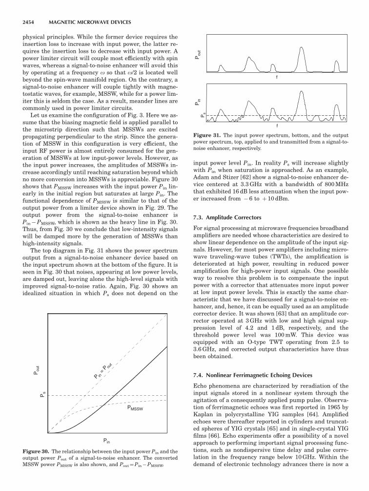
physical principles. While the former device requires theinsertion loss to increase with input power, the latter re-quires the insertion loss to decrease with input power. Apower limiter circuit will couple most efficiently with spinwaves, whereas a signal-to-noise enhancer will avoid thisby operating at a frequency o so that o/2 is located wellbeyond the spin-wave manifold region. On the contrary, asignal-to-noise enhancer will couple tightly with magne-tostatic waves, for example, MSSW, while for a power lim-iter this is seldom the case. As a result, meander lines arecommonly used in power limiter circuits.
Let us examine the configuration of Fig. 3. Here we as-sume that the biasing magnetic field is applied parallel tothe microstrip direction such that MSSWs are excitedpropagating perpendicular to the strip. Since the genera-tion of MSSW in this configuration is very efficient, theinput RF power is almost entirely consumed for the gen-eration of MSSWs at low input-power levels. However, asthe input power increases, the amplitudes of MSSWs in-crease accordingly until reaching saturation beyond whichno more conversion into MSSWs is appreciable. Figure 30shows that PMSSW increases with the input power Pin lin-early in the initial region but saturates at large Pin. Thefunctional dependence of PMSSW is similar to that of theoutput power from a limiter device shown in Fig. 29. Theoutput power from the signal-to-noise enhancer isPin�PMSSW, which is shown as the heavy line in Fig. 30.Thus, from Fig. 30 we conclude that low-intensity signalswill be damped more by the generation of MSSWs thanhigh-intensity signals.
The top diagram in Fig. 31 shows the power spectrumoutput from a signal-to-noise enhancer device based onthe input spectrum shown at the bottom of the figure. It isseen in Fig. 30 that noises, appearing at low power levels,are damped out, leaving alone the high-level signals withimproved signal-to-noise ratio. Again, Fig. 30 shows anidealized situation in which Ps does not depend on the
input power level Pin. In reality Ps will increase slightlywith Pin when saturation is approached. As an example,Adam and Stizer [62] show a signal-to-noise enhancer de-vice centered at 3.3 GHz with a bandwidth of 800 MHzthat exhibited 16 dB less attenuation when the input pow-er increased from � 6 to þ10 dBm.
7.3. Amplitude Correctors
For signal processing at microwave frequencies broadbandamplifiers are needed whose characteristics are desired toshow linear dependence on the amplitude of the input sig-nals. However, for most power amplifiers including micro-wave traveling-wave tubes (TWTs), the amplification isdeteriorated at high power, resulting in reduced poweramplification for high-power input signals. One possibleway to resolve this problem is to compensate the inputpower with a corrector that attenuates more input powerat low input power levels. This is exactly the same char-acteristic that we have discussed for a signal-to-noise en-hancer, and, hence, it can be equally used as an amplitudecorrector device. It was shown [63] that an amplitude cor-rector operated at 3 GHz with low and high signal sup-pression level of 4.2 and 1 dB, respectively, and thethreshold power level was 100 mW. This device wasequipped with an O-type TWT operating from 2.5 to3.6 GHz, and corrected output characteristics have thusbeen obtained.
7.4. Nonlinear Ferrimagnetic Echoing Devices
Echo phenomena are characterized by reradiation of theinput signals stored in a nonlinear system through theagitation of a consequently applied pump pulse. Observa-tion of ferrimagnetic echoes was first reported in 1965 byKaplan in polycrystalline YIG samples [64]. Amplifiedechoes were thereafter reported in cylinders and truncat-ed spheres of YIG crystals [65] and in single-crystal YIGfilms [66]. Echo experiments offer a possibility of a novelapproach to performing important signal processing func-tions, such as nondispersive time delay and pulse corre-lation in the frequency range below 10 GHz. Within thedemand of electronic technology advances there is now a
Pin
PMSSW
Ps
P in =
P out
Pou
t
Figure 30. The relationship between the input power Pin and theoutput power Pout of a signal-to-noise enhancer. The convertedMSSW power PMSSW is also shown, and Pout¼Pin�PMSSW.
f
Ps
f
Pou
tP
in
Figure 31. The input power spectrum, bottom, and the outputpower spectrum, top, applied to and transmitted from a signal-to-noise enhancer, respectively.
2454 MAGNETIC MICROWAVE DEVICES

renewed interest in the use of ferrimagnetic echoingdevices.
Among many nonlinear systems capable of producingan echoed signal (e.g., cyclotron echo, plasma echo, molec-ular echo, phonon echo, and spin echo), only ferrimagneticecho can show amplification. This feature renders theferrimagnetic echo phenomena in a very unique positionfor device applications. Ferrimagnetic echo is concernedmainly with the reservoir of the electron spin system pro-vided by a YIG crystal that is nearly the perfect mediumfor signal storage. Thus, in view of the extremely narrowFMR linewidth (0.3 Oe at X band) the damping action ac-companying the spin motion in the YIG crystal is verysmall; once the spins are put in motion, they will continuethe motion indefinitely in time exhibiting very little at-tenuation. The lifetime of the magnons in a YIG crystal isvery long, usually exceeding 1 ms. Ferrimagnetic echo sig-nals are shown at the top of Fig. 6 in conjunction with in-termodulation signals shown at bottom that are inducedby a ferrite junction when excited at high power. We imag-ine that at the time instant t¼ � t a signal pulse is appliedto the YIG crystal setting the spins in precessional motion.Before the spin motion damps out, a pump pulse is appliedat the time instant t¼ 0, which is so intense that nonlinearinteraction is aroused in the spin system. Due to the (odd)cubic nature of the interaction, the process of time conju-gation is recalled, which reverses the timescale for thestored signal such that the spins begin to precess in theopposite direction. As a consequence, at time t¼ t ( 1 ms)the original signal pulse recovers, which appears as theimage, or replica, of the original signal echoed back by thepump pulse (see Fig. 6, the top diagram).
However, we must emphasize that if the cubic interac-tion is local in nature, no amplification is possible for theechoed signals, as occurs in the other nonlinear systemsinvolving only isolated echoing sites. For ferrimagneticecho the nonlinear interaction is brought about by thedipolar field interacting with the nonlocal spin wavesshowing a long-range dependence (this nonlocal interac-tion can be described in terms of a Green function whosekernel shows a 1/r dependence [25,26], see Eq. (100)below). As such, the echoed signal can show amplification,receiving power from the pump pulse not only to duplicatethe signal waveform to result in an echo but also to am-plify the echoed signal to high intensity. The amplificationgain can be as large as 100, as measured experimentally[64] and calculated theoretically [25,26].
Ferrimagnetic echo experiments are carried out usingcrystal YIG bulk or thin-film materials in the presence of ahigh-magnetic-field gradient (E1 kOe/cm). In order to ob-tain high amplification gain, the YIG material needs to beclamped between two polycrystalline poles to effectivelysuppress the demagnetizing field. Theoretically it hasbeen demonstrated that the DC demagnetizing field hasadverse effect in reducing the echo gain to zero [25,26].This result is consistent with Suhl’s finding [13] that theDC demagnetizing field is apt to enhance spin-wave in-stability resulting in subsidiary absorption during micro-wave resonance measurements.
Finally, we want to point out the similarities betweenthe ferrimagnetic echo signals and the intermodulation
noise observed in a ferrite circulator junction [24]. Asshown at bottom of Fig. 6, two RF signals at adjacent fre-quencies f1 and f2 will couple each other to form intermod-ulation noises at frequencies 2f1� f2 and 2 f2� f1.Intermodulation signals grow rapidly with power, whichmay be identified as clicking noises in a telephone line.Actually, both the echoing signals and the intermodula-tion noises are generated through the same cubic interac-tion terms in the equation of motion, Eq. (64). The onlydifference is that echo is a phenomenon in the time do-main, whereas intermodulation is manifested in the fre-quency domain. While the DC demagnetizing field hasbeen shown to have adverse effects in influencing the echogain in the time domain, it has also been demonstratedthat the same demagnetizing field will enhance the inter-modulation level in a circulator junction [24]. Therefore,the DC demagnetizing field needs to be suppressed orminimized in nonlinear studies of ferrites applied at highpower concerning the phenomena of spin-wave instabili-ties, the echo gain, and the intermodulation noise.
8. MAGNETIC SOLITONS
It is widely recognized that the study of nonlinear equa-tions and their solutions is of great importance in manyareas of physics. Of particular importance are nonlinearwave equations that admit large-amplitude solitary waveor soliton solutions that retain their shape during propa-gation. Such solutions have received considerable atten-tion by elementary particle physicists since they may beregarded as extended particle-like solutions of nonlinearfield equations. The study of solitary waves has provedfruitful in many areas of condensed-matter physics aswell, for example, in theories of Bloch walls that separatedomains in magnetic materials [3], structural phase tran-sitions [67], liquid helium 3He [68], 2D fluxons in Joseph-son weak-link junction [69], and low-temperature chargedensity wave condensates [70]. Engineering applicationsprefer solitonlike wavepackets or pulses to be formed inmaterials allowing the carried information to be transmit-ted over long distance without experiencing much atten-uation and dispersion, such as for the study of optical [71]and microwave [72] magnetic envelope solitons. In thissection Bloch wall solitons and magnetic microwave en-velope solitons, referred to in general as magnetic solitons,are briefly introduced.
The first documented observation of the solitary wavewas made in 1834 by the Scottish scientist John ScottRussell [73]. While observing the movement of a canalbarge, Scott Russell noticed a novel type of water wave onthe surface of the canal, in the form of a long bell-shapedwave that emerged and traveled down the channel—it didnot cause rippling of the water, instead it remained stableand localized without change of waveform and diminutionof speed over a distance about 2 miles in propagation. Thistype of water wave is now known as KdV solitons, short-ened for Kortweg and de Vries, who first successfully dem-onstrated the underlying mathematical solutions in 1895.The other two well-known soliton systems are associatedwith the sine Gordon and the nonlinear Schrodinger
MAGNETIC MICROWAVE DEVICES 2455

equations, describing the kinetics and dynamics of mag-netic Bloch walls and microwave magnetic envelope soli-tons, respectively, discussed in the section.
In a nonlinear system that admits soliton-like solu-tions, two kinds of elementary exciations are possible: (1)particles with a finite amplitude in excitation called sol-iton/antisoliton, or bright/dark solitons, which possesses afinite mass; and (2) massless particles, with an infinites-imal excitation amplitude, called quasiparticles. Exam-ples of solitons/antisolitons are electrons/positrons, and soforth, and quasiparticles are phonons, magnons, photons.Solitons and anti-solitons are topological entities, some-times called ‘‘kinks’’, whose waveform shapes are self-bal-anced so that dispersion imposed by the wave equationcancels exactly the nonlinear contribution from the am-plitude of wave excitation. Thus, solitons and antisolitonscarry shape integrity along with their motion, retainingtheir respective waveform shapes after the collision pro-cesses, similar to those massive particles observed in thephysical world. Furthermore, like particles and antiparti-cles, a soliton can collide with an antisoliton, resulting inpair annihilation, ending up with radiations in the form ofmassless particles. Although losses can be readily added tothe system, they will not affect the waveform shapes ofsolitons and antisolitons. Rather, the added loss terms inthe equation of motion can merely introduce dampingforces impeding the particles’ mobility in their kinetic mo-tion. At a given temperature the thermodynamic quanti-ties of the system, which describe the equilibrium states ofsolitons/antisolitons and the massless particles, can all becalculated, and phase transition can result at a Currietemperature in a manner analogous to that induced bysoft-phonon/displacive modes, as described in Ref. 67. Thefollowing section describes domain wall solitons and mi-crowave envelope solitons.
8.1. Magnetic Bloch Wall Soliton
A Bloch wall defines a magnetic transition layer that sep-arates two magnetic domains of opposite magnetization.That is, inside a magnetic Bloch wall the magnetizationvector reverses its direction undergoing 1801 in-plane ro-tation in a manner so as to minimize the total free energyimposed by the uniaxial anisotropy and the exchangeterms defined for HA and HE, respectively, following Eq.(18). Besides Bloch walls, the process of magnetization re-versal can also take place by assuming 1801 out-of-planerotation, giving rise to Neel walls, which are not discussedin this section. After applying the Lagrangian equationutilizing the energy densities given by Eq. (15), one ob-tains the following equation governing the dynamic mo-tion of a magnetic Bloch wall [3]
@2C@t2þ sin C�
@2C@x2¼ � f sin
C2� G
@C@t
þB cosC2
@2Ry
@x@tþ sin
C2
@2Rz
@x@t
� �
ð97Þ
where c denotes twice the azimuthal angle of the magne-tization vector swinging away from the easy axis, the z
axis, and Ry and Rz are the y and z components of the dis-placement fields. In Eq. (97) f, G, and B are dimensionlessparameters characterizing the magnitudes of the othercoupling terms, including the external driving force (theZeeman field), the Gilbert damping term, and the magne-toelastic constant of the medium, respectively. Here, x de-notes the direction normal to the Bloch wall surface. InEq. (97) the right-hand-side (RHS) terms may be treatedas perturbations to the left-hand-side (LHS) terms, whichrenders the original sine-Gordon equation, describing anddefining the unperturbed profile, kinetics, and dynamicsof magnetic Bloch wall solitons/anti-solitons. Namely, thefirst term is associated with the kinetic energy of a sine-Gordon soliton (of a unified mass or inertia), and the sec-ond and the third terms are potential energies, arisingfrom the uniaxial anisotropy, and the normalized ex-change interaction, respectively. The effects of externalmagnetic driving f, the Gilbert damping G, and the mag-netoelastic coupling B in influencing the soliton’s profileand its subsequent motion can thus be calculated [3]. Astability analysis on the mobility of a Bloch wall soliton/anti-soliton has also been performed in Ref. 3, discussed inconjunction with Slonzewski’s formula, which assumedthe low-magnetization limits.
8.2. Magnetic Microwave Envelope Soliton
In the absence of an externally applied RF signal field theresultant equation of motion up to the third order in RFmagnetization m is, from Eq. (9)
dm
dt¼ gez� Hom� Ms �
m .m
2MS
� �
hd �2A
MS
� �
r2mþlg
dm
dt
� �
;
ð98Þ
where H0 denotes the externally applied DC magneticfield normalized with respect to Ms, the saturation mag-netization, and A and l denote the exchange stiffness andGilbert damping constant introduced following Eq. (18),respectively; the nonlinear term comes from Eq. (46) as-suming large excursion angle of the magnetization vectoraway from the z axis, the applied field direction. In Eq.(98) hd denotes the dipole field induced by the rf-magne-tization m, all normalized with respect to Ms. Assumingthe magnetostatic limit, the relationship between hd andm is specified by Eq. (24). Or
hd¼ ð1=m0ÞrCr .m ð99Þ
where the Green function operator C is defined, upon op-eration on a regular function f(r) as
Cf ðrÞ¼
Z
all spaced3r0
1
jr� r0jf ðr0Þ ð100Þ
which represents the nonlocal effect characteristics of adipole field [25,26]. However, if one insists on a local ap-proximation enforcing the dipole field to be equal to the rf
2456 MAGNETIC MICROWAVE DEVICES

magnetization, or
hd¼ ð1=m0Þm ð101Þ
Eq. (98) becomes
dfdt¼
� jg Hof�MS
m0
1�jfj2
2
� �
f�2A
MSr2fþ
lg
dfdt
� �
; ð102Þ
where
f¼ðmx � jmyÞ=MS ð103Þ
denotes the (normalized) circularly polarization field.From Eq. (102) one recognizes immediately the (damped)nonlinear Schrodinger equation [73], which admits solu-tions for microwave magnetic envelope solitons whose ex-istence has been reported by various authors [74–76].
Although we have derived the desired equation of mo-tion characteristic of microwave magnetic envelope soli-tons [Eq. (102)], caution is needed regarding use of thenonlinear term that was derived on the basis of the localassumption of the dipole field, Eq. (101), which was pro-posed intuitively without justification. Actually the samelocal assumption, Eq. (101), was used by Hermann in for-mulating the ferrimagnetic echo–gain calculations [77].Although Hermann was able to predict the existence offerrimagnetic echos, the calculated echo gain factors weretwo orders smaller than actually measured [64,65], indi-cating the insufficiency or inadequacy of the local dipolefield assumption, Eq. (104). As such, Eq. (102) can poseonly limited value; it at best leads to heuristic conclusionsthat in Eq. (102) the cubic interaction term, due to thelarge excursion angle of spins performing precessionalmotion, and dispersion, due to the exchange couplingamong spins, constitute the two necessary ingredientsfor the generation of solitonlike solutions coincident withthe nonlinear Schrodinger equation under the very crudeassumptions. Only after the nonlocal nature of the dipolefield rigorously treated in the equation of motion, can theformulation predict reliable results, Eqs. (99) and (100).Also, Eq. (98) assumes an infinite system for which theboundary conditions have been ignored. In real measure-ments finite samples such as single-crystal YIG films arenormally used in conjunction with the microstrip launchercircuits shown in Fig. 24. As such, boundary conditionsneed to be included and the demagnetizing field effects tobe explicitly considered [Eq. (66)]. The demagnetizing fieldhas been found effective in triggering profound processesin ferrite samples undergoing high-power excitations, asobserved in ferrimagnetic echo, intermodulation, andstabilities measurements. More work in these areas isneeded.
Two different types of envelope solitons, bright solitonsand dark solitons, or solitons and antisolitons, can prop-agate in nonlinear waveguiding dispersive media. Brightand dark solitons may be classified as dynamical and to-pological, respectively. The term ‘‘dynamical’’ for bright
solitons means that these pulses are essentially nonlinearwavepackets for which the carrier signal maintains a con-stant phase over the pulse. The term ‘‘topological’’ denotesthe fact that the passage of a single dark soliton modifiesthe medium or the medium response in some critical way.‘‘Dark envelope’’ solitons may be described in terms of acarrier signal of constant amplitude that has a dip in am-plitude at the soliton position. If this dip goes completelyto zero, one has a black soliton. If the minimum power atthe dip is nonzero, one has a gray soliton. Dark envelopesolitons have a nonzero jump in phase for the carrier sig-nal as one crosses the dip. In the case of black solitons, thisjump in phase is exactly 1801.
Observation of self-generated bright and dark micro-wave magnetic envelope solitons in ferrite films can befound in Refs. 75 and 76, respectively. Interaction betweenmicrowave magnetic envelope solitons and between mi-crowave magnetic envelope solitons and continuous mag-netostatic waves can be found in Refs. 74 and 78,respectively. Before ending this section, we note that itwas generally observed that formulation, propagation,and decay of microwave magnetic envelope solitons werealways accompanied by the generation of high-wavenum-ber spin waves, indicating that the equation of motion ofthe system is more involved than described by the simplenonlinear Schrodinger equation, Eq. (102), which allowsfor isolation of stable clean solitons and continuous waves.Thus, a complete description of the nonlinear spin systemhas to recruit the long-range dipole field, Eqs. (99) and(100), not only to faithfully describe soliton behaviors butalso to understand interactions between themselves andbetween themselves and continuous waves, including thescattering processes involving three magnons and the re-sultant (modulation) instabilities of the system. Theseareas are discussed further in Refs. 79–81.
9. MAGNETOOPTIC DEVICES
At optical frequencies the Polder permeability tensor of aferrite specimen is nearly isotropic with the diagonalelement mE1 and off-diagonal element kE10�5, as canbe calculated from Eqs. (11) and (12). Although small, theresultant magnetic anisotropy or gyrotropy can be mea-sured using a laser optical beam. On incidence, the re-flected and the transmitted beams will carry themagnetization information of the specimen, resulting innot only a rotation in polarization but also a change inreflectivity and transmission. These are called magneto-optic Kerr and Faraday effects for reflection and transmis-sion measurements, respectively. Kerr and Faraday effectshave been used in observing the dynamic processes ofdomain wall motion in a ferromagnetic metal or a ferri-magnetic insulator sample, respectively [82].
The most important devices utilizing magnetooptic cou-pling for electronic signal processing applications concernthe scattering process between photons and magnons.This process is called Bragg diffraction, where in a ferri-magnetic medium a photon of momentum P is scatteredby a magnon of momentum k, resulting in a photon ofmomentum Pþk. This interaction is second order in
MAGNETIC MICROWAVE DEVICES 2457

nature and is described a term of gm0 mk�hP includedwith the right hand side of Eq. (7). Here mk denotes themagnetization field of the magnon and hP is the magneticfield of the photon. As such, the photon wave is said to bemodulated by the magnetization wave, carrying alongwith it the electronic information after scattering. Be-cause of the nature of a second-order interaction, Braggdiffraction between photons and magnons, or MSWs in amagnetic film, is not very prominent, and only about 4%light diffraction was observed experimentally with a 7-mminteraction length for MSSW excitations approaching sat-uration [83].
Optical techniques are being increasingly utilized tomeet the ever-growing data rate requirements of signalprocessing and communication applications. A key ele-ment to such applications has been acoustooptic modula-tors based on Bragg diffraction between photons andphonons. A large time–bandwidth product (TBW; i.e.,time delay of acoustic signal in traversing the opticalbeam times signal bandwidth) is usually desirable.However, acoustic waves cannot be efficiently excitedat frequencies above 2 GHz. Instead, magnetoopticdevices offer the potential of large TBW modulation di-rectly at microwave frequencies. The diffraction of guidedoptical waves by MSW is analogous to optical diffractionby a SAW and has the potential to enhance a wide varietyof integrated optical applications such as spectrumanalyzer, optical filters, deflectors, switches, and con-volvers.
The basic theories of the MSW–optical interaction, in-cluding the development of expressions for optical diffrac-tion efficiency and coupling factor as a function of theMSW power and other relevant parameters, has been de-rived by Fisher [83]. The theory applies to the collinearconfiguration, shown in Fig. 32, with the MSW travelingin a direction parallel or antiparallel to the optical beam,as well as to the transverse configuration, shown inFig. 33, where the MSW travels at a 901 angle to the op-tical beam. In Figs. 32 and 33 prisms are used to guideoptical beams onto the YIG layers that are transparent
to lightwave propagation. In Figs. 32 and 33 the MSWconfiguration may be replaced by the superstrate struc-ture shown in Fig. 3. To achieve good optical properties,the YIG film is usually highly doped, mainly by bismuth.As such, Bragg diffraction of guided optical waves byMSSWs and MSFVWs has been demonstrated in the con-figurations shown in Figs. 32 and 33, and the conversionsbetween TE and TM modes have been experimentally ob-served from 1 to 6.5 GHz [83].
In experimental solid-state physics photons are usedas instrumentation tools to probe the phonon spectra insolids. This is termed Brillouin light scattering. Analo-gously, Brillouin light scattering can be applied to a ferritesample to study the magnon or spin-wave spectrum in thepresence of solitons as well as to investigate the role ofspin waves at the onset of instabilities [84,85]. In a ferritea photon can create or absorb a magnon. The photonwill be scattered in the process; its wavevector willchange from k to k0 and its frequency from o to o0.Suppose a magnon is created with a wavevector K andangular frequency O. The kinematics of the collision orscattering event are simple. According to the conservationof energy
o¼o0 þO ð104Þ
and per the wavevector selection rule
k¼k0 þK ð105Þ
where, for simplicity, we do not include the possibility thatthe scattering may be combined with a Bragg diffractioninvolving a reciprocal lattice vector of the crystallinestructure of a ferrite crystal. When o, o0, k, and k0 areknown, O and K can thus be determined.
In conclusion, MSW optical devices are currently in anearly stage of development, and their basic feasibility hasbeen demonstrated. However, they are expected to lead toa variety of high-performance integrated optical signalprocessing devices.
Ground plane YIG film
(Power in)
(Power out)
TM
TE
GGG
Figure 33. Transverse configuration for MSW and optical beams.Bragg diffraction of the guided optical wave by an MSW inducesconversion between orthogonally polarized optical modes.
Ground planeYIG film
(Power out)
TM
TE
GGG
(Power in)
MSW
Figure 32. Collinear configuration with codirectional MSW andoptical beams. Due to Bragg diffraction between the optical beamand the MSWs, the original TM guided optical beam is scatteredinto a TE beam with deflected angle of propagation.
2458 MAGNETIC MICROWAVE DEVICES

10. ANTIREFLECTION LAYERS AND ABSORBING LAYERS
To date microwave or millimeter-wave antireflection lay-ers and absorbing layers are almost exclusively used forradome design applications. Because of the highly classi-fied nature of this topic, not much data have been pub-lished in the literature. In this section we discuss only theconcepts that lead to the construction of microwave ormillimeter-wave antireflection and absorbing layers. Noexplicit design parameters are given here. By definition,an antireflection/absorbing layer is placed on top of a sub-strate such that an incident microwave or millimeter-wave beam will be totally transmitted/absorbed whenpassing across the layer without causing reflection. Thelayer should be functional over a frequency range as broadas possible to be independent of the incident angle andpolarization of the incident beam.
To realize the design of an antireflection layer, we con-sider first the case of normal incidence of the incidentbeam. According to the transmission-line theory, one con-cludes immediately that the first-order solution would re-quire the layer to behave like a quarter-wave transformer.This implies that the layer shall possess a thickness equalto one quarter the wavelength with a characteristic im-pedance
ZL¼ ðZ0ZSÞ1=2
ð106Þ
where
Z0¼m0
e0
� �1=2
ð107Þ
ZS¼mS
eS
� �1=2
ð108Þ
where Z0 (ZS) is the characteristic impedance of air (sub-strate) and e0 (eS) and m0 (mS) are the permittivity and per-meability of air (substrate), respectively. When broaderbandwidth is desired, higher-order solutions are required,and this results in a multilayer system with progressivelychanging electromagnetic parameters matching the im-pedance difference between air and substrate.
For an absorbing layer design the air impedance canalso be matched by a multilayer system with progressivelyincreasing damping parameters such that the series of thelayers satisfies the transformer matching requirement.Thus, we use the same impedance transformer theory forthe design of absorbing layers, except that the impedancesof the layers are now complex numbers, since the permit-tivity and permeability of the layers are complex numbers.As such, the incident wave damps out when it passesthrough the layer system before arriving at the substrate.
When oblique-angle incidence is considered, the imped-ance transformer theory can be generalized using thetransfer matrix technique [41,86]. The present problemis to determine an optimal layer system design allowingfor polarization independent operation over a frequencyband and angle range on beam incidence as broad as pos-sible. Also, the design task is subject to a very importantconstraint requiring the thickness of the layers to be
minimal, since at microwave and/or millimeter frequen-cies a practical layer system should be thin enough com-pared to the wavelength of the waves propagating in air.The design is in general not a trivial problem, and efficientcomputer algorithms are needed.
Once an optimal multilayer system is determined, theremaining task is to synthesize it using real materials.Unfortunately, nature does not provide general materialscovering the whole range of electromagnetic parameters.Instead, artificial materials need to be developed. The firstkind of artificial materials include particle compositeswhere dielectric particles [87], metal-shelled particles[88], ferrite particles [89,90], and graphite powders areembedded in a matrix epoxy such that the effective per-mittivity, permeability, and/or conductivity of the compos-ite can be controlled over the desired frequency band byadjusting the mixing faction of the particles.
The second class of artificial materials is quite new; itinvolves periodic patterns of metal strips or grooves (sur-face relief gratings) to be fabricated on top of a layer sur-face. In fact, when electromagnetic waves interact withperiodic structures much finer than the wavelength, theydo not diffract, but instead reflect and transmit as if theywere encountering a nonstructured medium. Effectivefield theory describes the interaction between electromag-netic waves and such subwavelength structures by repre-senting a region of subwavelength heterogeneity in termsof a homogeneous material possessing a single set of ef-fective electromagnetic parameters: permittivity, perme-ability, and conductivity [91]. Actually, the antireflectionstructures consisting of surface relief gratings can befound on the cornea of certain night-flying moths, andthe first scientists to investigate antireflection-structuredsurfaces for application in the visible or near-infraredportion of the spectrum worked to replicate moth eye sur-faces [92].
Antireflection means establishing a resonant structureon the substrate surface that is able to ‘‘capture’’ the in-cident electromagnetic signal forming standing modes soas to dissipate the captured energy, converting it into heatbefore it reaches the substrate. In this sense an antire-flection layer is a sheet of absorbent. Two kinds of reso-nant structures are possible. Standing modes can beformed along the propagation direction, or the longitudi-nal direction, of the signal by constructing a quarter-wavetransformer [Eq. (106)] or a transformer of high order, asdiscussed previously. Alternatively, standing modes can beformed along the transverse directions. For example, met-al patches or meshes of a diameter equal to one-half thewavelength of the incident electromagnetic waves can bedeployed in front of the substrate surface accompanied byan dissipation layer responsible for wave damping. Mul-tiple antireflection layers can be stacked together to joint-ly capture and damp a broadband signal, thereby realizingthe broadband operation.
BIBLIOGRAPHY
1. B. Lax and K. J. Button, Microwave Ferrites and Ferrimag-
netics, McGraw-Hill, New York, 1962.
MAGNETIC MICROWAVE DEVICES 2459

2. J. C. Slater, Quantum Theory of Matter, 2nd ed., McGraw-Hill,New York, 1972.
3. H. How, R.C. O’Handley, and F. R. Morgenthaler, Soliton the-ory for realistic domain wall dynamics, Phys. Rev. B
40(7):4809 (1989).
4. C. Vittoria, Microwave Properties of Magnetic Films, WorldScientific, Singapore, 1993.
5. S. Chikazumi and S. H. Charap, Physics of Magnetism, Wiley,New York, 1964.
6. C. Kittel, Introduction to Solid State Physics, 4th ed., Wiley,New York, 1971.
7. F. R. Morgenthaler, Dynamic magnetoelastic coupling in fer-romagnets and antiferromagnets, IEEE Trans. Magn. Mag-8(1):130 (1972).
8. H. How, Microstrip antennas, in Encyclopedia of Electrical
and Electronics Engineering, Wiley, Hoboken, NJ, 2003.
9. H. How and C. Vittoria, Surface retarded modes in multilay-ered structures: Parallel magnetization, Phys. Rev. B
39(10):6823 (1989).
10. H. How and C. Vittoria, Bulk and surface retarded modes inmultilayered structures: Antiparallel magnetization, Phys.Rev. B 39(10):6831 (1989).
11. R. E. Collin, Foundations for Microwave Engineering, Mc-Graw-Hill, New York, 1966.
12. C. Vittoria and N. D. Wilsey, Magnetostatic wave propagationlosses in an anisotropic insulator, J. Appl. Phys. 45:414(1974).
13. H. Suhl, The theory of ferromagnetic resonance at high signalpowers, J. Phys. Chem. Solids 1:209 (1957).
14. K. Nakamura, S. Ohta, and K. Kawasaki, J. Phys. C 15:L143(1982).
15. F. M. de Aguiar and S. M. Rezende, Observation of subhar-monic routes to chaos in parallel-pumped spin waves in yt-trium iron garnet, Phys. Rev. Lett. 56:1070 (1986).
16. F. Bloch, Z. Physik 61:206 (1930); 74:295 (1932).
17. F. R. Morgenthaler, J. Appl. Phys. 31:95S (1960).
18. E. Shloemann, J. J. Green, and U. Milano, J. Appl. Phys.31:386S (1960).
19. H. Bosma, On the principle of stripline circulation, Proc. IEE
B 109:137 (1962).
20. H. Bosma, On stripline Y-junction at UHF, IEEE Trans. Mi-crowave Theory Tech. MTT-12:61 (1964).
21. C. E. Fay and R. L. Comstock, Operation of the ferrite junc-tion circulators, IEEE Trans. Microwave Theory Tech. MTT-13:15 (1965).
22. Y. S. Wu and F. J. Rosenbaum, Wide-band operation of mi-crostrip circulators, IEEE Trans. Microwave Theory Tech.MTT-22:849 (1974).
23. E. Schloemann and R. E. Blight, Broad-band stripline circu-lators based on YIGand Li-ferrite single crystals, IEEE Trans.Microwave Theory Tech. MTT-34:1394 (1986).
24. H. How, T.-M. Fang, C. Vittoria, and R. Schmidt, Non-linear intermodulation coupling in ferrite circulator junc-tions, IEEE Trans. Microwave Theory Tech. MTT-45(2):245(1997).
25. H. How and C. Vittoria, Theory on amplified ferrimagneticechoes, Phys. Rev. Lett. 66(12):1626 (1991).
26. H. How and C. Vittoria, Amplification factor of echo signals inferrimagnetic materials, IEEE Trans. Microwave TheoryTech. MTT-39(11):1828 (1991).
27. W. H. Von Aulock, ed., Handbook of Microwave Ferrite Mate-
rials, Academic Press, New York, 1965.
28. M. E. Hines, Reciprocal and nonreciprocal modes of propaga-tion in ferrite stripline and microstrip devices, IEEE Trans.Microwave Theory Tech. MTT-19:442–451 (1961).
29. H. How, C. Vittoria, and C. Carosella, Novel filter design in-corporating stripline Y-junction circulators, IEEE Trans. Mi-
crowave Theory Tech. MTT-39(1):40 (1991).
30. H. How, C. Vittoria, and C. Carosella, Experiments on wide-stopband filters utilizing asymmetric circulators, IEEE Trans.
Microwave Theory Tech. MTT-40(1):161 (1992).
31. H. How, R. Schmidt, and C. Vittoria, Design of six-port ferritejunction circulators: Theory and experiments, IEEE Trans.Microwave Theory Tech. MTT-42(7):1272 (1994).
32. N. Zeina, H. How, and C. Vittoria, Self-biasing circulators op-erating at Ka band utilizing M-type hexagonal ferrites, IEEE
Trans. Magn. Mag-28(5):3219 (1992).
33. H. How, T. M. Fang, C. Vittoria, and R. Schmidt, ‘‘Losses inStripline/Microstrip Circulators,’’ IEEE Trans. Microwave
Theory Tech. MTT-46(5):543, 1997.
34. H. S. Newman and C. M. Krowne, Analysis of ferrite circula-tors by 2-D finite-element and recursive Green’s functiontechniques, IEEE Trans. Microwave Theory Tech. MTT-46(2):167–177 (1998).
35. H. How, S. W. McKnight, S. A. Oliver, P. M. Zavracky, N. E.McGruer, and C. Vittoria, Influence of non-uniform magneticfield on a ferrite junction circulator, IEEE Trans. Microwave
Theory Tech. MTT-47(10), 1982–1989 (1999).
36. H. How, S. A. Oliver, S. W. McKnight, P. M. Zavracky, N. E.McGruer, and C. Vittoria, Theory and experiment of thin-filmjunction circulator, IEEE Trans. Microwave Theory Tech.MTT-46:1645–1653 (Nov. 1998).
37. K. C. Kupta, R. Garg, and I. J. Bahl, Microstrip Lines and
Slotline, Artech, House, Norwood, MA: 1979.
38. H. How, R. Seed, C. Vittoria, D. B. Chrisey, and J. S. Horwitz,Microwave characteristics of superconducting coplanar wave-guide resonator, IEEE Trans. Microwave Theory Tech. MTT-41(3):255 (1993).
39. T. Miura and Y. Konishi, New lumped element circulator byceramic integrated circuit technology, IEEE Trans. Broad-
cast. 4(3):101–106 (1995).
40. J. Deutsch and B. Wieser, Resonance isolator and Y-circulatorwith lumped element at VHF, IEEE Trans. Magn. Mag-2(3):278–282 (1966).
41. H. How, X. Zuo, E. Hokanson, and C. Vittoria, Calculated andmeasured characteristics of a microstrip line fabricated on aY-type hexaferrite substrate, IEEE Trans. Microwave Theory
Tech. MTT-50(5):1280–1288 (2002).
42. E. Schloemann, R. I. Joseph, and I. Bady, Spin-wave insta-bility in hexagonal ferrites with a preferential plane, J. Appl.
Phys. 34(3):672 (1963).
43. A. V. Nazarov and C. E. Patton, Effect of large magnetocrys-talline anisotropy on the spin wave linewidth in Zn-Y hexag-onal ferrite, J. Appl. Phys. 93(11):9195 (2003).
44. R. G. Cox, C. E. Patton, M. A. Wittenauer, P. Kabos, and L.Chen, Spin wave instability in single crystal Zn-Y hexagonalferrite at 8.93 GHz, J. Appl. Phys. 89(8):4454 (2001).
45. A. V. Nazarov, R. G. Cox, and C. E. Patton, High power mi-crowave properties of Zn-Y hexagonal ferrite-parallel pump-ing size effects, J. Appl. Phys. 92(7):3890 (2002).
46. S. V. Lebedev, C. E. Patton, and M. A. Wittenauer, Frequencyand temperature dependence of the ferromagnetic resonancelinewidth in single crystal platelets and pulsed laserdeposited films of barium ferrite, J. Appl. Phys. 91(7):4426,(2002).
2460 MAGNETIC MICROWAVE DEVICES

47. H. How, Method and Apparatus of Obtaining Phase Shift Us-
ing Non-Reciprocal Resonator, U.S. Patent 6,483,393 (Nov. 19,2002).
48. D. M. Pozar, Radiation and scattering characteristics of mi-crostrip antennas on normally biased ferrite substrates, IEEE
Trans. Anten. Propag. AP-30:1084 (1992).
49. V. L. Taylor, J. C. Setjares, and C. V. Smith, Jr., MSWtermi-nations, Proc. IEEE Ultrasonic Symp. 1980, p. 562.
50. M. R. Daniel, J. D. Adam, and T. W. O’Keeffe, Linearly dis-persive delay lines at microwave frequencies using magneto-static waves, Proc. IEEE Ultrasonics Symp. 1979, p. 806.
51. K. W. Chang, J. M. Owens, and R. L. Carter, Linearly disper-sive delay control of magnetostatic surface wave by variableground-plane spacing, Electron. Lett. 19:546 (1983).
52. F. R. Morgenthaler, Field gradient control of magnetostaticwaves for microwave signal processing applications, Proc.RADC Microwave Magnetic Workshop, 1981, p. 133.
53. L. R. Adkins and H. L. Glass, Dispersion control in magne-tostatic delay lines by means of multiple magnetic layer struc-tures, Proc. IEEE Ultrasonic Symp. 1980, p. 526.
54. W. S. Ishak and K. W. Chang, Magnetostatic wave devices formicrowave signal processing, Hewlett-Packard J. 10 (1985).
55. J. D. Adam, An MSWtunable bandpass filter, Proc. IEEE Ul-
trasonic Symp., 1985, p. 157.
56. J. P. Castera and P. Hartemann, Adjustable magnetostaticsurface wave multistrip directional coupler, Electron. Lett.16:195 (1980).
57. J. P. Castera, New configurations for magnetostatic wave de-vices, Proc. IEEE Ultrasonic Symp. 1980, p. 514.
58. J. P. Castera and P. Hartemann, A multipole magnetostaticwave resonator filter, IEEE Trans. Magn. MAG-18:1601(1982).
59. K. W. Chang and W. S. Ishak, Magnetostatic forward volumewaves straight-edge resonators, Proc. IEEE Ultrasonic Symp.1986, p. 473.
60. G. S. Uebele, Characteristics of ferrite microwave limiters,IEEE Trans. Microwave Theory Tech. 7:18 (1959).
61. S. N. Stizer, and H. Goldie, A multi-octave frequency selectivelimiter, IEEE Digest MTT-S:326 (1983).
62. J. D. Adam and S. N. Stizer, A magnetostatic signal to noiseenhancer, Appl. Phys. Lett. 36:485 (1980).
63. W. S. Ishak, E. Reese, and E. Huijer, Magnetostatic wave de-vices for UHF band applications, J. P. Parekh, ed., Circuits
Systems Signal Processing, 1985, Vol. 4, p. 285.
64. D. E. Kaplan, Magnetostatic mode echo in ferromagnetic res-onance, Phys. Rev. Lett. 14(8):254 (1965).
65. D. E. Kaplan, R. M. Hill, G. F. Herrmann, Amplified ferri-magnetic echoes, J. Appl. Phys. 40(3):1164 (1969).
66. F. Bucholtz, D. C. Webb, and C. W. Young, Jr., Ferrimagneticechoes of magnetostatic surface wave modes in ferrite films, J.
Appl. Phys. 56(6):1859 (1984).
67. J. A. Krumbansl and J. R. Schieffer, Phys. Rev. B. 11:3535(1975).
68. K. Maki and P. Kumar, Phys. Rev. B. 14:118 (1976).
69. K. Nakajima, Y. Sawada, and Y. Onodera, J. Appl. Phys.46:5272 (1975).
70. M. J. Rice, A. R. Bishop, J. A. Krumhansl, and S. E. Trullinger,Phys. Rev. Lett. 36:432 (1976).
71. G. P. Agrawal, Nonlinear Fiber Optics, Academic Press, Bos-ton, 1989.
72. B. A. Kalinikos, N. G. Kovshikov, and A. N. Slavin, Sov. Phys.
JETP 67:303 (1988).
73. R. K. Dodd, J. C. Eilbeck, J. D. Gibbon, and H. C. Morris,Solitons and Nonlinear Wave Equations, Academic Press,London, 1982.
74. K. G. Kovshikov, B. A. Kalinikos, C. E. Patton, E. S. Wright,and J. M. Nash, Formation, propagation, reflection, and col-lision of microwave envelope solitons in yttrium iron garnetfilms, Phys. Rev. B 54:15210 (1996).
75. M. M. Scott, B. A. Kalinikos, and C. E. Patton, Self-generationof bright microwave magnetic envelope soliton trains in fer-rite films through frequency filtering, Appl. Phys. Lett.78(7):970 (2001).
76. B. A. Kalinikos, M. M. Scott, and C. E. Patton, Self-generationof fundamental dark Solitons in magnetic films, Phys. Rev.
Lett. 84(20):4697 (2000).
77. G. F. Hermann, R. M. Hill, and D. E. Kaplan, Phys. Rev. B2:2587 (1970).
78. M. M.Scott, Y. K. Fetisov, V. T. Synogach, and C. E. Patton,Suppression of microwave magnetic envelope solitons by con-tinuous wave magnetostatic wave signals, J. Appl. Phys.88(7):4232 (2000).
79. V. T. Synogach, Y. K. Fetisov, C. Mathieu, and C. E. Patton,Ultrashort microwave pulses generated due to three magnoninteractions, J. Appl. Phys. 85(10):2184 (2000).
80. B. A. Kalinikos, N. G. Kovshikov, and A. N. Slavin, Envelopesolitons and modulation instability of dipole-exchange mag-netization waves in yttrium iron garnet films, Sov. Phys.
JETP 67(2):303 (1988).
81. M. M. Scott, B. A. Kalinikos, and C. E. Patton, Spatial recur-rence for nonlinear magnetostatic wave excitations, J. Appl.
Phys. 94(9):5877 (2003).
82. J. M. Florczak and E. D. Dahlberg, Detecting two magneti-zation components by the magneto-optical Kerr effect, J. Appl.Phys. 67:7520 (1990).
83. A. D. Fisher, Optical signal processing with magnetostaticwaves, in J. P. Parekh, ed., Circuits Systems Signal Process-
ing, 1985, Vol. 4, p. 265.
84. H. Y. Zhang, P. Kabos, H. Xia, P. A. Kolodin, and C. E. Patton,Brillouin light scattering observation of the nonlinear spin-wave decay in yttrium iron garnet thin films, Phys. Rev. B
61(1):22 (2000).
85. C. Mathieu, V. T. Synogatch, and C. E. Patton, Brillouin lightscattering analysis of three-magnon splitting processes in yt-trium iron garnet films, Phys. Rev. B 67:10440 (2003).
86. H. How, W. Tian, and C. Vittoria, AC Hall effect in multilay-ered semiconductors, J. Lightwave Technol. 15(6):1006 (1997).
87. L. Rayleigh, On the influence of obstacles arranged in rect-angular order upon the properties of a medium, Phil. Mag.34:481 (1982).
88. H. How, W. A. Spurgeon, and C. Vittoria, The Microwave
Properties of Conducting Spherical Shells, Technical Report,U.S. Army Materials Technology Laboratory, MTL TR 90-7,February, 1990.
89. H. How and C. Vittoria, Demagnetizing energy and magneticpermeability tensor of spheroidal magnetic particles dis-persed in cubic lattices, Phys. Rev. B 43(10):8094 (1991).
90. H. How and C. Vittoria, The polder tensor of spherical mag-netic particles in cubic lattices: An exact solution in multipoleexpansion, Phys. Rev. B 44(17):9362 (1991).
91. D. H. Raguin and G. M. Morris, Antireflection structuredsurfaces for the infrared spectral region, Appl. Opt. 32:1154(1993).
92. P. B. Clapham and M. C. Hutley, Reduction of lens reflectionby the ‘‘moth eye’’ principle, Nature (Lond.) 244:281 (1973).
MAGNETIC MICROWAVE DEVICES 2461

MAGNETIC RESONANCE IMAGING
ANDREW WEBB
University of Illinois atUrbana–Champaign
Urbana, Illinois
1. INTRODUCTION
Magnetic resonance imaging (MRI) is one of the major ra-diological diagnostic modalities in the clinic. More than 20million exams per year are carried out in the UnitedStates alone. A large number of academic and commerciallaboratories are involved in the development of new hard-ware, data processing algorithms and applications. Stud-ies can be performed on size scales ranging from humansto single neurons. One factor linking many of the mostrecent developments in MRI is the trend towards higherstatic magnetic fields. Higher fields provide many bene-fits, which will be outlined in this article, but also presentconsiderable challenges in engineering design. Since the‘‘operating frequency’’ of the system and associated hard-ware is proportional to the strength of the static magneticfield, high-frequency analysis of system design, as well asthe interactions between electromagnetic radiation andthe human body are increasingly important areas of re-search. As shown in Fig. 1, MRI now spans almost theentire radiofrequency spectrum.
The MRI signal arises from protons in the body, pri-marily water but also lipid. The patient is placed inside asuperconducting magnet, which produces a static mag-netic field several tens of thousands times stronger thanEarth’s magnetic field. Each proton, which is a chargedparticle with angular momentum, can be considered asacting as a small magnet. The protons align in two con-figurations, with their magnetic fields aligned either par-allel or antiparallel to the direction of the large staticmagnetic field, with slightly more found in the parallelstate. The protons precess around the direction of thestatic magnetic field, analogously to a spinning gyroscopeunder the influence of gravity. The frequency of precessionis proportional to the strength of the static magnetic field.Application of a weak radiofrequency (RF) field causes the
protons to precess coherently, and the sum of all the mag-netic moments of the precessing protons is detected as aninduced voltage in a tuned detector coil. Spatial informa-tion is encoded into an image using magnetic field gradi-ents [1,2]. These impose a three-dimensional linearvariation in the magnetic field present within the patient.As a result of these variations, the precessional frequen-cies of the protons depend on their position within thebody. The frequency and phase of the precessing magne-tization are detected by the RF coil, and the analog signalis digitized. An inverse two-dimensional Fourier trans-form is performed to convert the time-domain signal intothe spatial domain to produce the image. By varying dataacquisition parameters, differential contrast between softtissues can be introduced into the image. Figure 2 shows ablock diagram of an MRI system. Many of the subsystemsare described in detail later in this article.
2. BASIC PRINCIPLES
For this article, only proton MRI will be considered, al-though useful spatial information from other nuclei suchas 23Na, 19F, and 31P can also be obtained. In proton MRIthe signal comes essentially from the protons in water,with a minor component from those in fat. From a quan-tum mechanical standpoint, the proton possesses two nu-clear energy levels, which correspond to the z componentof the magnetic moment of the proton being aligned eitherparallel or antiparallel to the applied static magnetic field,as shown in Fig. 3.
The energy gap between the two energy levels is givenby
DE¼ghB0
2pð1Þ
In order to stimulate transitions between the two energylevels, an oscillating magnetic field must be applied at afrequency o, such that
ho2p¼
ghB0
2p) o¼ gB0 ð2Þ
1 10 50 100 500 1000 2000
Frequency/MHz
Human MRI systems
0.1T 0.2T 0.5T 1.5T1T 3T 4T 7T 8T 9.4T
4.7T 17.6T
Animal MRI systems
Figure 1. Operating frequencies of humanand animal MRI systems. The correspondingstatic magnetic field strengths are given intesla (T).
2462 MAGNETIC RESONANCE IMAGING
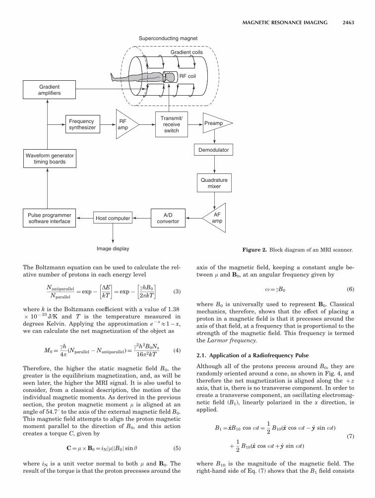
The Boltzmann equation can be used to calculate the rel-ative number of protons in each energy level
Nantiparallel
Nparallel¼ exp�
DE
kT
� �
¼ exp�ghB0
2pkT
� �
ð3Þ
where k is the Boltzmann coefficient with a value of 1.38� 10� 23 J/K and T is the temperature measured indegrees Kelvin. Applying the approximation e� xE1� x,we can calculate the net magnetization of the object as
M0¼gh4pðNparallel �NantiparallelÞ¼
g2h2B0Ns
16p2kTð4Þ
Therefore, the higher the static magnetic field B0, thegreater is the equilibrium magnetization, and, as will beseen later, the higher the MRI signal. It is also useful toconsider, from a classical description, the motion of theindividual magnetic moments. As derived in the previoussection, the proton magnetic moment m is aligned at anangle of 54.71 to the axis of the external magnetic field B0.This magnetic field attempts to align the proton magneticmoment parallel to the direction of B0, and this actioncreates a torque C, given by
C¼ m�B0¼ iNjmjjB0j sin y ð5Þ
where iN is a unit vector normal to both m and B0. Theresult of the torque is that the proton precesses around the
axis of the magnetic field, keeping a constant angle be-tween m and B0, at an angular frequency given by
o¼ gB0 ð6Þ
where B0 is universally used to represent B0. Classicalmechanics, therefore, shows that the effect of placing aproton in a magnetic field is that it precesses around theaxis of that field, at a frequency that is proportional to thestrength of the magnetic field. This frequency is termedthe Larmor frequency.
2.1. Application of a Radiofrequency Pulse
Although all of the protons precess around B0, they arerandomly oriented around a cone, as shown in Fig. 4, andtherefore the net magnetization is aligned along the þ zaxis, that is, there is no transverse component. In order tocreate a transverse component, an oscillating electromag-netic field (B1), linearly polarized in the x direction, isapplied.
B1¼ xxB10 cos ot¼1
2B10ðxx cos ot� yy sin otÞ
þ1
2B10ðxx cos otþ yy sin otÞ
ð7Þ
where B10 is the magnitude of the magnetic field. Theright-hand side of Eq. (7) shows that the B1 field consists
Gradientamplifiers
Frequencysynthesizer
Superconducting magnet
Gradient coils
RF coil
Waveform generatortiming boards
Pulse programmersoftware interface
Image display
Host computerA/D
convertorAF
amp
Quadraturemixer
Demodulator
PreampTransmit/receiveswitch
RFamp
Figure 2. Block diagram of an MRI scanner.
MAGNETIC RESONANCE IMAGING 2463

of the sum of two rotating magnetic fields, one rotatingclockwise and the other anticlockwise. It can be shownthat only the clockwise rotating field interacts with thenuclear spins. Application of the B1 field at the Larmorfrequency rotates the net magnetization M0 toward the yaxis, creating a component of magnetization My, given by
My¼M0 sinðgB1tB1Þ¼M0 sin a ð8Þ
where a is the excitation tip angle. This process of tippingthe magnetization is shown in Fig. 4. After the RF pulse,the component of magnetization in the xy plane precessesaround B0 at the Larmor frequency.
2.2. Signal Detection
Signal detection involves placing an RF coil close to thesample. In its simplest form, this coil can be a single loopof wire. Faraday’s law states that, when the magnetic fluxenclosed by a loop of wire changes with time, a current isproduced in the loop, and a voltage is induced across the
ends of the loop. The induced voltage E is proportional tothe negative of the time rate of change of the magnetic flux(df/dt):
E / �dfdt
ð9Þ
The time-varying magnetic field produced by the preces-sion of the magnetization vectors results in a voltage in-duced in the RF coil. The requirement for a time-varyingmagnetic flux is the reason why only precessing magneti-zation in the xy plane gives rise to an NMR signal; the zcomponent does not precess and therefore produces novoltage. At higher strengths of the B0 field, the protonsprecess at a higher frequency [Eq. (6)], and the value ofdf/dt increases. Therefore, higher magnetic fields producehigher signal not only because of greater nuclear polar-izations [Eq. (4)] but also because of the higher voltageinduced in the RF coil. Overall, we obtain
E /g2h2B0Ns
16p2kTgB0 sin a ð10Þ
4�
=
E
E4�
Direction of B0
h 3=
Magnetic fieldpresent
E= − hB04�h
4��z= + h
�
�
E4�
E= + hB0
Antiparallel
Parallel
Nomagnetic field
Parallel
Antiparallel
�→
4�
=h 3
=�→
∆E
�z= −
(a) (b)
Figure 3. (a) Quantization of the magnitudeof the z-component of a proton’s angular mo-mentum means that the z component of theproton’s magnetic moment (mz) has two possi-ble physical orientations, parallel and antipar-allel, with respect to the direction of the mainmagnetic field—the value of the angle y is54.71; (b) in the absence of an external mag-netic field, there is only one energy level. Whenan external magnetic field is present, ‘‘Zee-man’’ splitting results in two energy levels,with more protons occupying the lower energylevel, corresponding to the proton magneticmoments being aligned parallel to the mainmagnetic field, than the higher energy level,corresponding to an antiparallel alignment.
B1,x B1,x
x
z
y
z
z z
y
yy
x
(a) (b)
(d)(c)
Figure 4. (a) Application of a B1 field (B1,x) alongthe x axis rotates the individual proton magneticmoments about the x axis toward the y axis; (c)After applying the B1 field for a certain time du-ration, the ‘‘cone’’ of magnetic moments has beenrotated by 901 (the magnetic moments continueto precess around the B0 axis); (b,d) the vectormodel representations of the effect of the B1 field.The initial longitudinal magnetization (Mz) hasbeen rotated into the transverse plane and hasbeen converted into transverse magnetization(My) along the y axis.
2464 MAGNETIC RESONANCE IMAGING

2.3. Relaxation
Each of the magnetization components Mz, Mx, and My
must return to their thermal equilibrium values overtime. The time evolutions of Mz, Mx, and My are charac-terized by the Bloch equations [3]
dMx
dt¼ gMy B0 �
og
� �
�Mx
T2
dMy
dt¼ gMzB1 � gMx B0 �
og
� �
�My
T2
dMz
dt¼ � gMyB1 �
Mz �M0
T1
ð11Þ
where T1 is the spin–lattice relaxation time and governsthe z component of magnetization and T2 is the spin–spinrelaxation time governing the transverse component. Inthe well-known rotating reference frame—a frame ofreference where the x0y0 axes rotate around B0 at theLarmor frequency—simple expressions can be obtainedfor the time evolution of longitudinal and transversemagnetization:
MzðtÞ ¼Mzðt¼ 0Þþ ½M0 �Mzðt¼ 0Þ�ð1� e�t=T1 Þ ð12Þ
MyðtÞ¼Myðt¼ 0Þe�t=T2
MxðtÞ¼Mxðt¼ 0Þe�t=T2
ð13Þ
As seen later in the article, image contrast dependsstrongly on the different T1 and T2 values for various tis-sues in the human body.
2.4. Magnetic Field Gradients
Three separate gradient coils are required to encode un-ambiguously the three spatial dimensions within the body.Since only the z component of the magnetic field interactswith the proton magnetic moments, it is the spatial vari-ation in the z component of the magnetic field which is
important. Image reconstruction is simplified consider-ably if the magnetic field gradients are linear over theregion to be imaged:
@Bz
@z¼Gz
@Bz
@x¼Gx
@Bz
@y¼Gy ð14Þ
By convention, for human studies the z direction lies alongthe head-to-foot axis, the y axis corresponds to the vertical(spine-to-abdomen) direction, and the x axis extends fromside to side. The gradient coils are designed (as discussedlater in this article) such that there is no additional con-tribution to the static magnetic field at the isocenter (z¼ 0,y¼ 0, x¼ 0) of the magnet, which means that the magneticfield at this position is simply B0. If a gradient Gz isapplied, the magnetic field Bz experienced by all nucleiwith a common coordinate z is
Bz¼B0þ zGz ð15Þ
where Gz has units of tesla (T) per meter or gauss (G) percentimeter (cm). The corresponding precessional frequen-cies (oz) of the protons, as a function of their position in z,is given by
oz¼ gBz¼ gðB0þ zGzÞ ð16Þ
In the rotating reference frame the precessional frequencyis
oz¼ g zGz ð17Þ
Analogous expressions can be obtained for the spatial de-pendence of the resonant frequencies in the presence ofthe x and y gradients.
The process of image formation can be broken downinto three components: slice selection, phase encoding,and frequency encoding. Examples of common imagingsequences are shown in Fig. 5. In the gradient echo se-quence the combination of a frequency-selective 901 pulse
TRTR
TE
TE
RF
Gslice
Gfreq
Gphase
Nr data points
Np
A/D
RF
Gslice
Gphase
Gfreq
A/D
t
�pe
90°
90°180°
(a) (b)
Figure 5. (a) Basic scheme for a gradient–echo imaging sequence and (b) for a spin–echosequence. In both cases the acquisition matrixsize is Nr � Np data points.
MAGNETIC RESONANCE IMAGING 2465

and the slice gradient tips protons within a thickness Do/gGslice, where Do is the frequency bandwidth of the pulse,into the transverse plane. Protons outside this slice arenot excited. Application of the phase encoding gradientGphase, denoted as the y direction here, imparts a spatiallydependent phase shift into the signal. During signal ac-quisition, the frequency encoding gradient (x direction)generates a spatially dependent precessional frequency inthe acquired signal. Overall, ignoring relaxation effects,the detected signal is given by
sðGy; tpe;Gx; tÞ /
Z
slice
Z
slicerðx; yÞe�jgGxxte�jgGyytpe dx dy ð18Þ
where r(x,y) is the spatially dependent proton density,specifically, the number of protons at a given x,y coordi-nate. Using the k-space formalism [4], this signal can beexpressed as
Sðkx; kyÞ /
Z
slice
Z
slicerðx; yÞ e�j2pkxxe�j2pkyydx dy ð19Þ
where the two variables kx and ky are defined as
kx¼g
2pGxt; ky¼
g2p
Gytpe ð20Þ
This representation of the acquired data is particularlyuseful since the image can simply be reconstructed by aninverse two-dimensional Fourier transform.
rðx; yÞ¼Z 1
�1
Z 1
�1
Sðkx; kyÞeþ j2pðkxxþ kyyÞdkxdky ð21Þ
The k-space representation of the data is shown in Fig. 6.In the kx dimension Nr data points are acquired (seeFig. 5). The imaging sequence is repeated Np times, withthe phase encoding gradient incremented for each repeti-tion. This results in Np lines being acquired in the ky
direction.If the effects of T1 and T2 relaxation are taken into
account, it can be shown that in a gradient–echo sequence,the image intensity I(x,y) is given by
Iðx; yÞ /rðx; yÞð1� e�TR=T1 Þ e�TE=T�2 sin a
1� e�TR=T1 cos að22Þ
where T2� is the spin–spin relaxation time, including the
effects of magnetic field inhomogeneity. For a spin–echoimaging sequence, the corresponding expression is
Iðx; yÞ / rðx; yÞð1� e�TR=T1 Þe�TE=T2 ð23Þ
The times TR (repetition time) and TE (echo time) withinthe imaging sequence can be chosen to give different con-trasts in the image. For example, Fig. 7 shows the effects ofincreasing the TE on a simple brain scan.
The ability to produce many different contrast charac-teristics in images is one of the major advantages of MRIas a clinical diagnostic technique. Clinical applicationsinclude brain scanning (for tumors, hematomas, astro-cytomas, etc.), musculoskeletal (shoulder, knee, etc.), car-diac, and liver/kidney imaging. Contrast agents such asgadolinium DTPA and superparamagnetic iron oxide areoften used to highlight pathological features fromsurrounding healthy tissue [5]. Detailed descriptions ofclinical MRI can be found in Ref. 6.
3. HARDWARE DESIGN
The major hardware components of an MRI system arethe magnet, magnetic field gradients, and RF coil, in ad-dition to the receiver. The first three components involvesimilar analytical methods [7,8] to design, respectively, ahomogenous DC static magnetic field, linear spatially de-pendent rapidly switched magnetic fields, and high-frequency (60–750 MHz) resonators producing a uniformmagnetic field.
kx
ky
x
y
2D-IFFT
2D-FFT
(a) (b)
Figure 6. (a) The magnitude of the signal, S(kx,ky),from a scan of the human head (the center datapoints have the highest signal intensity and repre-sent the low-spatial-frequency components; datapoints at the extremities of k space correspond tothe high spatial frequencies); (b) a magnitude rep-resentation of the image produced by inverse two-dimensional Fourier transformation of the k-spacedata.
(a) (b)
Figure 7. Axial images of the brain acquired at 1.5 T. The imagein (a) is acquired with a TE value of 34 ms. Increasing the TEvalue to 102 ms produces the image in (b).
2466 MAGNETIC RESONANCE IMAGING

3.1. Superconducting Magnets
For all imaging studies performed at field strengths aboveB0.5 T, a superconducting magnet is required. For fieldsbelow this, permanent magnets can be used. In either casethe critical factors in magnet design are high homogeneityof the field [o1 part per million (ppm) over the sample],and a high degree of temporal stability(o50 Hz drift perhour). Almost all clinical superconducting magnets have acylindrical bore, approximately 1 m in diameter, whichencloses the magnetic field gradients, radiofrequency coil,and patient, as shown in Fig. 1. In order to create highstatic magnetic fields, it is necessary for the superconduc-tor to carry a large current, and this capability is pos-sessed only by certain alloys, particularly those made fromniobium–titanium. Below a critical temperature (9 K) andcritical magnetic field (10 T), once current has been fedinto such an alloy, this current will run through the wirewith constant magnitude essentially indefinitely. The su-perconducting alloy is formed into multistrand filamentsand interspersed within a conducting matrix. This ar-rangement can support a much higher critical currentthan a single, large-diameter superconducting wire. Thesuperconducting coils shown in Fig. 8 are housed in astainless-steel can containing liquid helium at a temper-ature of 4.2 K. This inner container is surrounded by aseries of radiation shields and vacuum vessels to minimizeheat transfer to the liquid helium. Liquid nitrogen is usedto cool the outside of the vacuum chamber and the radi-ation shields. Since heat transfer cannot be completelyeliminated, liquid nitrogen and liquid helium must be re-plenished on a regular basis.
The exact placement of the superconducting filamentswithin the magnet is designed to give the maximum fieldhomogeneity over the patient. The basic design consists ofa number of wire helices, or solenoids, of different diam-eters and separations, each wound along the major axis ofthe magnet. A typical layout is shown in Fig. 8.
For a single loop of wire, the field can be expressed as
Bzðr; yÞ¼X
1
n¼ 0
r
r0
� �n
BnPnðcos yÞ ð24Þ
where r0 is half the length of the region of interest and Pn
(cos y) is the standard Legendre polynomial of degree n.The design problem is to determine the optimum number,spacing, and diameter of wire loops such that the Bn co-efficients are zero up to the maximum order. The largerthe number of current-carrying elements that are present,the higher the order of the harmonics that can be mini-mized; however, one constraint is the total length of themagnet.
Slight errors in positioning the wires can lead to sig-nificant variations in the field uniformity, in which casethe Bz field is given by the complete solution to Laplace’equation. Additional coils of wire are added in series withthe main coil as superconducting correction coils. After themagnet has been energized by passing current into themajor filament windings, the current can be changed inthese correction coils to improve the homogeneity. Finetuning is performed by using a series of independentlywired coils at room temperature, termed ‘‘shim coils.’’ Theoperator can adjust the current in these coils for eachclinical examination, and so the magnet homogeneity canbe optimized for individual patients.
A strong magnetic field is also present outside the mag-net, and this can interfere with any electronic equipmentnearby. Machines with moving parts, such as inductionmotors, or any object with metallic elements must beplaced outside the fringe field; this creates an effective‘‘deadspace’’ around the magnet. In many clinical andacademic institutions space is limited, and so a reductionin the extent of the ‘‘stray’’ field is highly desirable.‘‘Active shielding’’ of a magnet uses secondary windings,placed outside the primary magnet windings, with thecurrent traveling in the opposite direction, in order tominimize the fringe field. Clearly, the presence of thesesecondary windings also reduces the field within thepatient, and so an increased current is now neededin the primary windings. The alternative method of ‘‘pas-sive magnet shielding’’ incorporates iron plates into themagnet exterior. The disadvantage of this method ofshielding is that the mass of the magnet is increased sig-nificantly.
3.2. Magnetic Field Gradient Coils
Three separate ‘‘gradient coils’’ are required to encode thex, y, and z dimensions of the sample. The requirements forgradient coil design are that the gradients are as linear aspossible over the region being imaged, that they are effi-cient in terms of producing high gradients per unit cur-rent, and that they have fast switching times for use inrapid imaging sequences. Copper is used as the conductor,with chilled-water cooling to remove the heat generated bythe current. Since the gradient coils fit directly inside thebore of the cylindrical superconducting magnet, the geo-metric design is usually also cylindrical. The simplest con-figuration for a coil producing a gradient in the z directionis a ‘‘Maxwell pair,’’ shown in Fig. 9a, which consists of twoseparate loops of multiple turns of wire, each loop con-taining equal currents I flowing in opposite directions. Inorder to estimate the distance between the two loops thatmaximizes the linearity of the gradient, the value of Bz is
z
Figure 8. Schematic of the layout of the su-perconducing wires to produce a homoge-neous magnetic field Bz within the patient.
MAGNETIC RESONANCE IMAGING 2467

first calculated
Bz¼m0Ia2
2½ðd=2� zÞ2þa2�1:5�
m0Ia2
2½ðd=2þ zÞ2þa2�1:5ð25Þ
where m0 is the permeability of free space and a is the ra-dius of the gradient set. The first term that can give anonlinear contribution is the third derivative, given by
d3Bz
dz3¼
15m0Ia2
2
4ðd=2� zÞ3 � 3ðd=2� zÞa2
½ðd=2� zÞ2þa2�9=2
(
þ4ðd=2þ zÞ3 � 3ðd=2þ zÞa2
½ðd=2þ zÞ2þa2�9=2
)
ð26Þ
This term becomes zero at a value of d¼aH3. The magneticfield produced by this gradient coil is zero at the center ofthe coil, and is linearly dependent on position in the zdirection over about one-third of the separation of the twoloops. The region over which the gradient is linear can beextended by adding other sets of coils in the axial dimension.
The x- and y-gradient coils are completely independentof the z-gradient coils. The derivation of gradient fieldlinearity for the transverse gradients is somewhat morecomplicated than for the Maxwell pair. The usual config-uration is to use four arcs of wire as shown in Fig. 9b. Thewire segments in the z direction do not produce a trans-verse component to the field, and the four outer arcs pro-vide return paths for the current. The Bz field produced byan arc on a cylinder of radius a is given by
Bzðr; y;fÞ
¼X
1
n¼ 0
X
n
m¼ 0
rnPmn ðAnm cos mfþBnm sin mfÞ Pnm cos y
ð27Þ
If the four inner arcs are placed symmetrically aroundz¼ 0, then Anm¼ 0 for all m, and Bnm¼ 0 if n or m is even.Equation (27) can now be expanded as follows:
Bzðr; y;fÞ¼ � B11r sin y sin fþB31r3P13 cos y sin f
þB33r3P33 cos y sin 3fþ � � �
ð28Þ
The first term is a linear function of y, but the other termsare nonlinear. The term in B33 can be made zero by settingthe angle c¼ 1201, and the term in B31 can be eliminatedby setting y0¼ 21.31 for z0¼ 2.57a. These results meanthat the separation between the arcs along the z axis isB0.8 times the radius of the gradient coil. From symmetryconsiderations the same basic design can be used for coilsproducing gradients in the x direction with the geometrysimply rotated by 901.
A second design criterion is that the current in thegradient coils should be switched on and off in the shortestpossible time. This reduces the time that must be allowedfor gradient stabilization in imaging sequences. This cri-terion is achieved by minimizing the inductance L of thegradient coils. A related issue is achieving high efficiencyZ, where Z is defined as the gradient strength per unitcurrent at the center of the gradient set. These three cri-teria (homogeneity, switching speed and efficiency) forjudging gradient performance can be combined into a so-called figure of merit b, defined as
b¼Z2
L
ffiffiffiffiffiffiffiffiffiffiffiffiffiffiffiffiffiffiffiffiffiffiffiffiffiffiffiffiffiffiffiffiffiffiffiffiffiffiffiffiffiffiffiffiffiffiffi
1
V
Z
BðrÞ
B0ðrÞ� 1
� �2
d3r
s ð29Þ
where B0(r) is the ‘‘desired’’ magnetic field, B(r) is the ac-tual magnetic field, and V is the volume of interest overwhich the integral is evaluated.
When the current in the gradient coils is switched rap-idly, eddy currents can be induced in nearby conductingsurfaces, such as the radiation shield in the magnet. Theseeddy currents, in turn, produce additional unwanted gra-dients in the sample that may decay only very slowly, evenafter the original gradients have been switched off. Theseeddy currents can result in image artifacts, and are par-ticularly problematic for sensitive measurements of diffu-sion coefficients and in localized spectroscopy. All gradientcoils in commercial MRI systems are now ‘‘actively shield-ed’’ to reduce the effects of eddy currents. Active shieldinguses a second set of coils placed outside the main gradientcoils, the effect of which is to minimize the stray gradientfields.
3.3. Radiofrequency Coils for MRI
Radiofrequency coils for MRI differ from conventional an-tennas in that they are designed to maximize the near-field magnetic energy that is stored in the patient. Thedesirable properties of such a coil include: (1) a homoge-neous B1 distribution within the patient, (2) minimumelectric fields within the patient since these lead to signal-to-noise ratio (SNR) losses and also to an increasedspecific absorption ratio (SAR; i.e., patient heating), (3)maximum B1 intensity per unit driving current, and (4)minimum resistive losses in the RF coil.
Since most RF coils are used to image either the brainor torso, the form of the coil is usually cylindrical as shownin Fig. 1. Assuming that this cylinder is infinitely long andcarries a surface current Js, given by
Js¼ zzJ0 sin f ð30Þ
I I
z0
�0
d
a
I I
z z
(a) (b)
Figure 9. (a) Schematic of a Maxwell gradient set that producesa linear magnetic field gradient in the z direction; (b) schematic ofa saddle geometry gradient set producing a linear magnetic fieldin the y direction.
2468 MAGNETIC RESONANCE IMAGING

the field inside the cylinder is given by
Bðr;fÞ¼ � rrX
1
m¼ 1
mrm�1ðAm cos mfþBm sin mfÞ
þ ffX
1
m¼ 1
mrm�1ðAm sin mf� Bm cos mfÞ
ð31Þ
By applying boundary conditions at the cylinder surface(considering the B1 field created outside the cylinder), allthe Bm coefficients must be zero, and the only nonzero Am
coefficient is given by A1¼ � m0J0/2. Therefore
Bðr;fÞ¼m0J0
2ðrr cos f� ff sin fÞ¼ xx
m0J0
2ð32Þ
This shows that a perfectly uniform B1 field, directedalong the x direction, is produced by a sinusoidal currentalong the surface of a cylinder of infinite length. Of course,this configuration cannot be realized in practice, but thebasic tenet of coil design is to approximate this sinusoidalsurface current. The most common such realization iscalled the ‘‘birdcage’’ resonator [9], which is shown inFig. 10. The resonator is usually constructed in a high-pass configuration, with a series of equidistantly spaced‘‘rungs’’ and two ‘‘end rings.’’
The birdcage coil has multiple resonant modes. For ann-rung highpass birdcage the highest-frequency mode isthe so-called end-ring mode, the next n� 2 modes are each
doubly degenerate (the highest-frequency one produces ahomogeneous transverse B1 field), and there is a singlemode at the lowest frequency. Since the birdcage coil hastwo orthogonal, degenerate homogeneous modes, it can beoperated in quadrature; that is, it can produce a circularlypolarized B1 field. This reduces the power required for RFtransmission by a factor of 2, and increases the image SNRalso by a factor of
ffiffiffi
2p
. Practical implementation simplyinvolves splitting the transmitter pulse through a quad-rature hybrid, the two outputs of which are connected tothe coil at feedpoints that are physically 901 apart.
Impedance matching of the coil must be performed inorder to ensure maximum power transmission and effi-cient reception. Since amplifier outputs, transmission ca-bles, and preamplifier input impedances are almostexclusively 50O, this is the impedance to which the coilis matched at the Larmor frequency. A balanced imped-ance-matching network should be used to reduce electricfield losses in the sample, and the most common is a stan-dard pi-matching network, with variable capacitors to ad-just for different sample-dependent loads. Often, baluns orcabletraps are used to reduce currents traveling on theoutside of the transmission cable connecting to the coil.
Noise in MRI originates from the sample and also theRF coil. Coil losses are linearly dependent on the operat-ing frequency, and sample losses in human patients in-crease as the square of the operating frequency. Ingeneral, at low frequencies coil losses are dominant,whereas at high frequencies sample losses are the domi-nant factor. In all cases it is desirable to minimize the loss
Lk−1,k−1
Lk−1,k−1
Lk+1,k+1
Lk+1,k+1
Mk+1,k+1
Ck−1
Ck−1
Ik−1
Ck+1
Ck+1
Ik+1
Lk,k
Lk,k
Mk,k
Ck
Ck
Ik
(a) (b)
(c)
Figure 10. (a) Highpass birdcage coil; (b) equivalent circuit model for the highpass birdcage in-cluding the mutual inductance between individual loops; (c) photograph of a 12-leg birdcage coil fora 1.5-T system.
MAGNETIC RESONANCE IMAGING 2469

inherent in the coil, that is, to maximize the quality factorQ of the tuned circuit. At high magnetic field strengths thedimensions of the RF coil constitute a substantial fractionof the wavelength of the electromagnetic wave inside thepatient. This leads to a number of problematic issues, in-cluding increased radiative losses and nonuniform currentdistribution along the conductors, which reduces the B1
homogeneity. One way to minimize these effects is to de-sign the coil using distributed capacitance rather thandiscrete lumped elements. Thus, familiar elements in mi-crowave technology, such as transmission lines and cavi-ties, will potentially play an increasingly important role inthe design of high frequency coils. For example, one suchdesign, termed a transverse electromagnetic (TEM) reso-nator, has been used for human studies up to frequenciesof 300 MHz [10].
3.4. Mutually Decoupled Coil Arrays
In many MRI applications, it is not necessary to acquiresignal from the entire patient, but only from a localizedregion. In this case, a small ‘‘surface coil’’ can be placednext to the region of interest. Typically, this surface coil isa simple circular or square loop. Since the B1 field pro-duced from such a coil is very inhomogeneous, a larger-‘‘volume’’ coil, such as the birdcage described previously, isused for transmitting a homogeneous B1 field, and thesurface coil is used to receive the signal. Using the smallsurface coil in this way gives a local SNR much higherthan that from the volume coil alone, due to both the highintrinsic sensitivity of the small surface coil and the re-duced noise contribution from the patient. However, sincethere are now two circuits impedance-matched at thesame frequency in relatively close proximity, there canbe considerable coupling between the two circuits. Thiscoupling must be minimized, and is normally achievedusing active detuning of the surface coil during transmis-sion, and the volume coil during signal reception, via PINdiodes.
An extension of the surface coil concept is the design ofarrays of mutually decoupled surface coils [11,12], oftenmisleadingly called ‘‘phased arrays,’’ as shown schemati-cally in Fig. 11. The use of many coils requires that theimaging system has multiple receiver channels; as of2004, most commercial vendors have up to 32 such receiv-er channels. Each coil in the array is connected to a sep-arate preamplifier and receiver. Using such arrays, muchlarger imaging fields of view can be covered than with asingle small coil, while maintaining the high sensitivity ofthe individual small surface coils. Image reconstruction isnormally implemented using a simple sum-of-squares al-gorithm. The major engineering challenge is to reduce thecoupling between individual coils; this coupling introducesnoise correlation into the reconstructed image and reducesthe image SNR. Effective coil decoupling can be achievedby optimal overlapping of the coils, a process thatminimizes the mutual impedance between neighboringcoils, and also by using high-input impedance preamplifi-ers for each of the coils, which minimizes the currentspresent in the individual coils, and therefore the intercoilcoupling [11].
3.5. The MRI Receiver
The basic elements of an analog MRI receiver chain are apreamplifier, a one- or two-stage demodulator, a quadrature-phase-sensitive detector, lowpass filters, two second-stageaudio amplifiers with variable gain, and finally two analog-to-digital converters; the MRI receiver as such is very simi-lar to a conventional superheterodyne radio receiver.
Figure 12 shows the first stage of the receiver chainand the connections to the MRI coil. The purpose of thetransmit/receive (Tx/Rx) switch is to ensure that the high-power transmitted RF pulse does not leak into the receiv-er, and also that during signal reception all of the signalpasses to the preamplifier. During transmission of theRF pulse, diodes D1 and D2 are turned on and thereforeconduct. Diodes D3 and D4 are also in ON state, and thequarter-wavelength cable to ground provides a highimpedance, preventing current from traveling to the pre-amplifier. The received signal (typically of the order ofmillivolts) is several orders of magnitude lower than thetransmitted pulse, and so, during signal reception, alldiodes are OFF. The transmitter chain presents a highimpedance, and all the signal passes through the quar-ter-wavelength cable to the preamplifier. In certainimplementations the quarter-wavelength cable can bereplaced by a lumped-element circuit, typically a ‘‘pi’’ net-work with two capacitors and one inductor. Rather thanthe single set of diodes shown in the diagram, in practicemany sets of diodes are used.
The second stage of the receiver chain is shown inFig. 13. The first stage demodulates the signal from theLarmor frequency to an intermediate frequency (IF), typ-ically B10.7 MHz. A second demodulation stage to base-band can be used, but most modern scanners directlysample at the intermediate frequency. The signal entersa quadrature mixer to produce real and imaginary
(a) (b)
Figure 11. Schematic of a four-element one-dimensional MRIcoil array (a) and an eight-element two-dimensional MRI coilarray (b).
2470 MAGNETIC RESONANCE IMAGING

outputs. These pass through lowpass filters, the cutoff fre-quency of which depends on the particular data acquisitionparameters used in the image. After final amplification,the signal is digitized, typically with a resolution of 16 bits.
3.6. Direct Digital Synthesis and Digital Detection
The rapid spread of digital transmission and reception inthe communication industry has recently been mirrored inthe design of MRI systems, in particular the receiver. Us-ing digital filters, for example, enables a much better filtershape than for the analog case. In addition, the data canbe oversampled many times, which provides a higher SNRin the reconstructed image. Direct digital synthesis (DDS)has the advantage of faster frequency- and phase-contin-uous switching than does its analog counterpart. A com-plete DDS unit is available on-chip (e.g., the AD9854 fromAnalog Devices, with 48 bit frequency resolution and 14
bit phase resolution). A DDS chip typically consists of anaddress counter, a lookup table for production of the sinewave at the frequency of interest, and a digital-to-analogconverter. Although such chips are currently limited inthe highest frequency that can be produced, the imagefrequency output can potentially be used for such appli-cations.
4. ADVANCED TOPICS
4.1. Parallel Imaging
One of the major limitations of MRI, particularly incomparison with computed tomography and ultrasonicimaging, is the relatively slow data acquisition. The fun-damental limits on imaging speed are the time requiredfor current switching in the gradient coils, and the rela-tively large number of phase encoding steps (typically
D1
D2 D3 D4
Baluns
Impedance matching networks
MRI coil
Hybrid couplerTx/Rx switch
�/4
RFtransmitter
0 90
in out
Preamplifier
Figure 12. A schematic of the first stage ofthe receiver chain with a Tx/Rx switch used toisolate the receiver from the transmitter.
LPF
Mixer
cos (�0 - �IF)t
Oscillator
Preamplifier
Demodulator
90°
(A/D)1
(A/D)2
cos�IFt
LPF
LPF
Mixer
Mixer
Quadrature mixer Variable-gainaudio amplifiers
Figure 13. A schematic of the second stage ofthe receiver chain and analog-to-digital (A/D)conversion, where o0 is the Larmor frequency,oIF the intermediate frequency, and LPF a low-pass filter.
MAGNETIC RESONANCE IMAGING 2471
128–256) required for reasonable spatial resolution. Morerecently, a general class of imaging techniques, termedparallel imaging, have been developed that use the spatialinformation from an array of mutually decoupled coils toreduce the number of acquired phase encoding steps, andtherefore increase the imaging speed. Acceleration factorsof 4 in one-phase-encoding direction, and up to 10 in two-phase-encoding directions have been achieved.
The basic principle of parallel imaging is that it ispossible to reconstruct many lines of k space from a singleacquired line. The original method, termed simulta-neous acquisition of spatial harmonics (SMASH) [13],achieves this by using combinations of signals from anarray of surface coils to directly mimic the spatial encod-ing normally performed by phase encoding. In analogyto Eq. (19), the k-space signal acquired in the pth coil isgiven by
Spðkx;kyÞ /
Z
slice
Z
slicerðx; yÞCpðx; yÞe
�j2pkxxe�j2pkyydx dy
ð33Þ
where Cp(x,y) is the spatial distribution of the RF sensi-tivity for the pth coil in the array. If the array is con-structed appropriately, then a linear combination of theindividual coil sensitivities can be used to produce shifts inky that are identical to acquiring different phase encodingsteps
X
p
nðmÞp Spðkx; kyÞ �X
p
nð0Þp Spðkx; kyþmDkyÞ ð34Þ
where m is an integer, either positive or negative. For ex-ample, if m¼ þ 1, then the even lines in ky space could beacquired, and the odd lines synthesized from the (mea-sured) coil sensitivity profiles, thus reducing the data ac-quisition time by a factor of 2.
For image reconstruction without artifacts, the SMASHtechnique relies on accurate knowledge or a good estimateof the relative RF sensitivities of the component coils in thearray in order to determine the optimal complex weightsnðmÞp . Many improvements have been made to the originalimplementation; for example, the technique known as gen-eralized autocalibrating partially parallel acquisitions(GRAPPA) acquires additional autocalibration scan (ACS)lines. Data from multiple lines from all the coils are used tofit ACS lines in a single coil. This fit gives the weights,which are then used to generate the missing k-space linesfrom that particular coil. After this procedure has beenperformed for each coil in the array, the full set of imagescan be combined using an optimal sum-of-squares recon-struction. Using GRAPPA several problems such as sub-optimal image reconstruction, phase cancellation andinexact estimates of coil sensitivities are minimized.
An alternative parallel imaging strategy is the sensi-tivity encoding (SENSE) method [15], which provides anoptimized reconstruction if a perfectly accurate complexcoil sensitivity map can be obtained. If the acquired k-space data are reduced by a factor of R by skipping certaink-space lines, then inverse Fourier transformation of thedata leads to aliased images from all the coils in the array.
In order to reconstruct an accurate image of the sample,the true signals and folded signals have to be separated.This can be achieved since, in the image from each indi-vidual coil, signal superposition occurs with differentweights according to the local coil sensitivities. The una-liased components v of every aliased pixel can be obtainedby an appropriate linear combination of the pixel values inthe various single-coil images
v¼ ðSHC�1SÞ�1SHC�1a ð35Þ
where vector v contains the unaliased pixel values, athe aliased values, and S the complex coil sensitivi-ties; the superscript H represents the transposed com-plex conjugate, and C noise correlation in the receiverchannels.
In addition to speeding up data acquistion, partial par-allel imaging can also be used to improve image quality insingle-shot imaging techniques, where short T2 valueslead to image blurring. An example is shown in Fig. 14.
4.2. Dielectric and Penetration Effects at High Frequencies
As described previously, higher static magnetic fields re-sult in a higher image SNR, and are particularly advan-tageous in functional magnetic resonance imaging, forexample. However, as the Larmor frequency increases,the dimensions of the human patient (head or torso) be-come a significant fraction of the radiofrequency wave-length, and the B1 field distribution is distortedsignificantly by the patient [16,17]. In general, two com-peting effects arise from the dielectric and conductivityproperties of the patient. Materials with a high dielectricconstant, for instance water with er¼ 80, reduce the effec-tive wavelength within the patient, and can give rise todielectric resonances that produce areas of high signal in-tensity at the center of the object. For a dielectric cylinderwith radius a cm and length L cm, the resonant frequencyof the TE01d mode is given by
fMHz¼3400
affiffiffiffi
erp
a
Lþ 3:45
� �
ð36Þ
(a) (b)
Figure 14. Single-shot inversion recovery HASTE images in thelungs of a healthy volunteer acquired with an eight-element car-diac array: (a) conventional acquisition matrix 128 � 256 (207 msimaging time, interecho spacing 2.88 ms); (b) GRAPPA acquisition(acceleration factor 3) with matrix 256 � 256 (150 ms imagingtime, interecho time 0.96 ms). (Reproduced from Ref. 14, copy-right 2002, with permission from John Wiley & Sons.)
2472 MAGNETIC RESONANCE IMAGING

The conductivity of the sample, however, dampens thiseffect and reduces the penetration of the RF field. Sinceboth effects are highly frequency-dependent, the relativeeffects are manifested very differently at different fieldstrengths. Specifically, the wavelength is given by
l¼2p
ffiffiffiffiffiffiffiffiffiffiffiffiffiffiffiffiffiffiffiffiffiffiffiffiffiffiffiffiffiffiffiffiffiffiffiffiffi
o2m0e0er � jom0sp ð37Þ
At field strengths up to 7 T, the dominant effect is from thedielectric ‘‘focussing,’’ which is typically seen as a brightareas in the center of the patient, as shown in Fig. 15 [18].
BIBLIOGRAPHY
1. P. C. Lauterbur, Image formation by induced local interac-tions: Examples employing nuclear magnetic resonance, Na-
ture 242:190–191 (1973).
2. P. Mansfield and P. K. Grannell, NMR diffraction in solids, J.
Phys. C Solid State Phys. 6:L422–L426 (1973).
3. F. Bloch, Nuclear induction, Phys. Rev. 70:460–474 (1946).
4. S. Ljunggren, A simple graphical representation of Fourier-based imaging methods, J. Magn. Reson. 54:338–343 (1983).
5. W. Krause, ed., Magnetic Resonance Contrast Agents, Spring-er-Verlag, Berlin, 2002.
6. D. D. Stark, and W. G. Bradley, Jr., Magnetic Resonanceimaging, Vols. 1 and 2, 2nd ed., Mosby-Year Books, 1992.
7. C. -N. Chen and D. I. Hoult, Biomedical Magnetic Resonance
Technology, Adam Hilger, Bristol and New York, 1989.
8. J. -M. Jin, Electromagnetic Analysis and Design in Magnetic
Resonance Imaging, CRC Press, Boca Raton, FL, 1998.
9. C. E. Hayes, W. A. Edelstein, J. F. Schenck, O. M. Mueller, andM. Eash, An efficient, highly homogeneous radiofrequencycoil for whole-body NMR imaging at 1.5 T, J. Magn. Reson.63:622–628 (1985).
10. J. T. Vaughan, H. P. Hetherington, J. O. Otu, J. W. Pan, and G.M. Pohost, High frequency volume coils for clinical NMRimaging and spectroscopy. Magn. Reson. Med. 32:206–218(1994).
11. P. B. Roemer, W. A. Edelstein, C. E. Hayes, S. P. Souza, and O.M. Mueller, The NMR phased array, Magn. Reson. Med.16:192–225 (1990).
12. S. M. Wright, R. L. Magin, and J. R. Kelton, Arrays of mutu-ally coupled receiver coils: theory and application, Magn. Re-
son. Med. 17:252–268 (1991).
13. D. K. Sodickson and W. J. Manning, Simultaneous acquisitionof spatial harmonics (SMASH): Fast imaging with radiofre-quency coil arrays, Magn. Reson. Med. 29:681–688 (1993).
14. M. A. Griswold, P. M. Jakob, R. M. Heidemann, M. Nittka, V.Jellus, J. Wang, B. Kiefer, and A. Haase, Generalized auto-calibrating partially parallel acquisitions (GRAPPA). Magn.
Reson. Med. 47:1202–1210 (2002).
15. K. P. Pruessmann, M. Weiger, M. B. Schneidegger, and P.Boesinger, SENSE: Sensitivity encoding for fast MRI, Magn.Reson. Med. 42:952–992 (1999).
16. G. H. Glover, C. E. Hayes, N. J. Pelc, W. A. Edelstein, O. M.Muller, H. R. Hart, C. J. Hardy, M. O’Donnell, and W. D. Bar-ber, Comparison of linear and circular polarization for mag-netic resonance imaging, J. Magn. Reson. 64:277–270 (1985).
17. D. I. Hoult, Sensitivity and power deposition in a high-fieldimaging experiment, J. Magn. Reson. Imag. 12:46–67 (2000).
18. J. T. Vaughan, M. Garwood, C. M. Collins, W. Liu, L. Dela-Barre, G. Adriany, P. Andersen, H. Merkle, R. Goebel, M. B.Smith, and K. Ugurbil. 7 T vs. 4T: RF power, homogeneity,and signal-to-noise comparison in head images, Magn. Reson.
Med. 46:24–30 (2001).
FURTHER READING
E. M. Haake, R. W. Brown, M. R. Thompson, and R. Venkatesan,Magnetic Resonance Imaging: Physical Principles and Se-
quence Design, Wiley-Liss, 2000.
Z.-P. Liang, and P. C. Lauterbur, Principles of Magnetic ResonanceImaging. A Signal Processing Perspective, IEEE Press Seriesin Biomedical Engineering, IEEE Press, 2000.
R. R. Ernst, G. Bodenhausen, and A. Wokaun, Principles of Nu-
clear Magnetic Resonance in One and Two Dimensions, OxfordScience Publications, 1987.
C. P. Slichter, Principles of Magnetic Resonance, Springer-Verlag,1990.
MAGNETIC SHIELDING
DAVID W. FUGATE
Electric Research andManagement, Inc.
FRANK S. YOUNG
Electric Power ResearchInstitute
Shielding is the use of specific materials in the form ofenclosures of barriers to reduce field levels in some regionof space. In traditional usage, magnetic shielding refersspecifically to shields made of magnetic materials like ironand nickel. However, this article is more general becauseit covers not just traditional magnetic shielding but also
(a) (b)
Figure 15. Magnetic resonance images acquired at (a) a fieldstrength of 4 T (proton Larmor frequency 170 MHz) and (b) at afield strength of 7 T (proton Larmor frequency 300 MHz). Thepresence of a dielectric resonance at the higher field strength isclearly visible. (Reproduced from reference 18, copyright (2001),with permission from John Wiley & Sons.)
MAGNETIC SHIELDING 2473

shielding of alternating magnetic fields with conductingmaterials, such as copper and aluminum. In typicalapplications, shielding eliminates magnetic field interfer-ence with electron microscopes, computer displays (CRTs),sensitive electronics, or other devices affected by magneticfields.
Although shielding of electric fields is relatively effec-tive with any conducting material, shielding of magneticfields is more difficult, especially at extremely low fre-quencies (ELFs). The ELF range is defined as 3 Hz–3 kHz[1]. The selection of proper shield materials, shield geom-etry, and shield dimensions are all important factors inachieving a specified level of magnetic field reduction.Placing a shield around a magnetic field source, as shownin Fig. 1a, reduces the field magnitude outside the shield,and placing a shield around sensitive equipment, asshown in Fig. 1b, reduces the field magnitude inside theshield. These two options are often called ‘‘shielding thesource,’’ or ‘‘shielding the subject,’’ respectively.
Both examples in Fig. 1 illustrate shield geometry. Inmany applications, it is impractical or impossible (due tophysical constraints) to use an enclosure, and open shieldgeometries, also called partial shields, are required.Figure 2 shows two basic partial shield geometries, aflat-plate shield (a), and a channel shield (b). For theseconfigurations, the region where shielding occurs may belimited because the shield does not fully enclose the sourceor the subject, resulting in edge effects. A discussion of thegeometric aspects of shielding in contained in Ref. 2.
1. ELF SHIELDING VERSUS HIGH-FREQUENCY SHIELDING
Electric and magnetic fields radiate away from a source atthe speed of light c. In the time it takes a source alternat-ing with frequency f to complete one full cycle, these fieldshave traveled a distance l, known as the electromagnetic
wavelength:
l¼ c=f ð1Þ
At distances from a field source on the order of one wave-length and larger, the dominant parts of the electric andmagnetic fields are coupled as a propagating electromag-netic wave. If a shield is placed in this region, shieldinginvolves the interaction of electromagnetic waves with theshield materials. Any mathematical description must bebased on the full set of Maxwell’s equations, which in-volves calculating both electric and magnetic fields.Shielding of electromagnetic waves is often described interms of reflection, absorption, and transmission [3]. Be-cause wavelength decreases with increasing frequency,shielding at radio frequencies in the FM band(88–108 MHz) and higher typically involves the interac-tion of electromagnetic waves with shield materials.
At distances much less than one wavelength, the non-radiating portion of the fields is much larger than theradiating portion. In this region, called the ‘‘reactivenear-field region,’’ the coupling between the electric andmagnetic fields can be ignored, and the fields may be cal-culated independently. This is called a quasistatic descrip-tion. At 3 kHz (the upper end of the ELF band), awavelength in air is 100 km. Thus, for ELF field sources,one is in the reactive near-field region in all practicalcases, and a full electromagnetic solution is not required.Instead, one need focus only on interaction of the magneticfield or the electric field with the shield material, depend-ing on which field is being shielded. In some cases, shield-ing of the electric field with metallic enclosures isrequired. This article deals specifically with the shieldingof DC and ELF magnetic fields.
2. MAGNETIC FIELDS
Moving electric charges, typically currents in electricalconductors, produce magnetic fields. Magnetic fields aredefined by the Lorentz equation as the force acting on atest charge q, moving with velocity v at a point in space
F¼ qðv� mHÞ ð2Þ
in which H is the magnetic field strength with units ofamperes per meter and m is the permeability of the medi-um. By definition of the vector cross-product, the force ona moving charge is at right angles to both the velocityvector and the magnetic field vector. Lorentz forces pro-duce torque in generators and motors and focus electronbeams in imaging devices.
Unwanted, or stray magnetic fields deflect electronbeams in the same imaging devices, often causing inter-ference problems. Sources that use, distribute, or producealternating currents, like the 60 Hz currents in a powersystem, produce magnetic fields that are time-varying atthe same frequency.
Magnetic fields are vector fields with magnitude anddirection that vary with position relative to their sources.This spatial variation or field structure depends on the
Figure 1. (a) Shielding the source—placing a shield around afield source reduces the fields everywhere outside the shield; (b)shielding the subject—a shield placed around a sensitive devicereduces the fields from external sources.
Figure 2. Examples of open shield geometries: (a) flat plateshield, (b) inverted channel shield.
2474 MAGNETIC SHIELDING

distribution of sources. Equal and opposite currents pro-duce a field structure that can be visualized by plottinglines of magnetic flux, as show in Fig. 3. The spacing be-tween flux lines, or line density, indicates relative fieldmagnitudes, and the tangent to any flux line representsfield direction. Another way to visualize field structure isthrough a vector plot, shown in Fig. 4. Lengths of the ar-rows represent relative field magnitudes, and the arrowsindicate field direction.
Shield performance, or field reduction, is measured bycomparing field magnitudes before shielding with the fieldmagnitudes after shielding. In general, field reductionvaries with position relative to the source and shield.The shielding factor s is defined as the ratio of the shield-ed field magnitude B to the field magnitude B0 withoutthe shield present at a point in space:
s¼ jBj=jB0j ð3Þ
The shielding factor represents the fraction of the originalfield magnitude that remains after the shield is in place. A
shielding factor of zero represents perfect shielding. Ashielding factor of one represents no shielding, and shield-ing factors greater than one occur at locations where thefield is increased by the shield. It is incorrect to define theshielding factor as the ratio of the fields on opposite sidesof a shield. Shielding factor is often called shielding effec-tiveness (SE), expressed in units of decibels (dB):
SE ðdBÞ¼ � 20 log10 jBj=jB0j ð4Þ
Shielding effectiveness is sometimes alternatively defineas the inverse of the shielding factor, the ratio of unshield-ed to shielded fields at a point, but it is really a matter ofpreference. For example, a shielding effectiveness of twodefined in this manner represents a twofold reduction,that is, the field is halved by the shield and the shieldingfactor is 0.5. When fields are time-varying, shielding istypically defined as the ratio of RMS magnitudes.
3. SHIELDING MECHANISMS
Although shielding implies a blocking action, DC and ELFmagnetic field shielding is more aptly described as alter-ing or restructuring magnetic fields by the use of shieldingmaterials. To illustrate this concept, Fig. 5a shows a fluxplot of a uniform, horizontal, magnetic field altered(Fig. 5b) by the introduction of a ferromagnetic material.
These are two basic mechanisms by which shield ma-terials alter the spatial distribution of magnetic fields,thus providing shielding. They are the flux-shuntingmechanism and the induced-current mechanism [5].
Figure 3. The lines of magnetic flux illustrate the field structureassociated with one or more sources. The density of flux lines in-dicates the relative field strength and the tangent to any line in-dicates the field direction at that point.
Figure 4. A vector plot graphically illustrates both field strengthand direction as a function of position.
Figure 5. (a) Horizontal uniform field (b) altered by introductionof a ferromagnetic material; illustrates the concept that shieldingis the result of induced sources in the shield material.
MAGNETIC SHIELDING 2475

3.1. Flux Shunting
An externally applied magnetic field induces magnetiza-tion in ferromagnetic materials. (All materials have mag-netic properties, but in most materials these propertiesare insignificant. Only ferromagnetic materials haveproperties that provide shielding of magnetic fields.) Mag-netization is the result of electrons acting as magneticsources at the atomic level. In most matter, these sourcescancel one another, but electrons in atoms with unfilledinner shells make a net contribution, giving the atoms amagnetic moment [6]. These atoms spontaneously aligninto groups called domains. Without an external field, do-mains are randomly oriented and cancel each other. Whenan external field is applied, the Lorentz forces align someof the domains in the same direction, and together, thedomains act as a macroscopic magnetic field source. A fa-miliar magnetic field source is a bar magnet, which ex-hibits permanent magnetization even without an appliedfield. Unlike a permanent magnet, most of the magneti-zation in ferromagnetic shielding materials goes awaywhen the external field is removed.
Basic ferromagnetic elements are iron, nickel, and co-balt, and the most typical ferromagnetic shielding mate-rials are either iron-based or nickel-based alloys (metals).Less common as shielding materials are ferrites such asiron oxide.
Induced magnetization in ferromagnetic materials actsas a secondary magnetic field source, producing fields thatadd vectorially to the existing fields and change the spa-tial distribution of magnetic fields in some region of space.The term flux shunting comes from the fact that a ferro-magnetic shield alters the path of flux lines so that theyappear to be shunted through the shield and away fromthe shielded region, as shown by the example in Fig. 6.Flux-shunting shielding is often described in terms ofmagnetic circuits as providing a low-reluctance path formagnetic flux.
Permeability m is a measure of the induced magnetiza-tion in a material. Thus, permeability is the key propertyfor flux-shunting shielding. The constitutive law
B¼ mH ð5Þ
relates magnetic flux density B to the magnetic fieldstrength H. More typically used, relative permeability is
the ratio of permeability in any medium to the permeabil-ity of free space, mr¼ m/m0. Nonferrous materials have arelative permeability of one, and ferromagnetic materialshave relative permeabilities much greater than one, rang-ing from hundreds to hundreds of thousands. In thesematerials, permeability is not constant but varies with theapplied field H.
The nonlinear properties of a ferromagnetic materialcan be seen by plotting flux density B, as the applied fieldH is cycled. Figure 7 shows a generic B–H plot that illus-trates hysteresis. When the applied field is decreased froma maximum, the flux density does not return along thesame curve, and plotting one full cycle forms a hystereticloop. A whole family of hysteretic loops exists for any fer-romagnetic material as the amplitude of field strength His varied. The area of a hysteretic loop represents the en-ergy required to rotate magnetic domains through one cy-cle. Known as hysteretic losses, this energy is dissipated asheat in the shield material.
For effective flux-shunting shielding, the flux density ina magnetic material should follow the applied field closely.However, it is obvious from the hysteretic loop of Fig. 7that B does not track H. B lags H, as seen by the fact thatthere is a residual flux density (nonzero B) when H hasreturned to zero and that B does not return to zero until Hincreases in the opposite direction. Thus, soft ferromag-netic materials with narrow hysteretic loops are best forshielding, in contrast to hard ferromagnetic materialswith wide hysteretic loops, typically used as permanentmagnets and in applications such as data storage.Hysteretic curves illustrating ‘‘soft’’ and ‘‘hard’’ ferromag-netic materials are shown in Fig. 8.
At very low field levels relative permeability starts atsome initial value (initial permeability) increases to amaximum as the applied field is increased, and then de-creases, approaching a relative permeability of one as thematerial saturates, as shown in Fig. 9. Saturation occursbecause there is a limit to the magnetization that can beinduced in any magnetic material. In Fig. 7, the decreas-ing slope at the top and bottom of the curves occurs as thelimit of total magnetization is reached. When a materialsaturates, it cannot provide additional shielding.
For shielding alternating magnetic fields via fluxshunting, the key property is AC permeability, DB/DHthrough one cycle. Although Fig. 7 shows a hysteresis
Figure 6. Example of the flux-shunting mechanism. The regioninside a ferromagnetic duct is shielded from an external, hori-zontal magnetic field.
Figure 7. Typical B–H curves showing how nonlinear propertiesof ferromagnetic materials result in a hysteretic loop as the ap-plied field H is cycled.
2476 MAGNETIC SHIELDING

curve that swings from near saturation to near saturationin both directions, a hystersis curve caused by a very smallalternating field in the presence of a large DC field mightlook like Fig. 10. In this case, the ac permeability is lessthan the DC permeability, B=H. In addition, the DC fieldcreates a constant magnetization that affects the time-varying magnetization. Figure 11 shows how AC perme-ability for a small alternating field is reduced with in-creasing DC field. This plot, called a ‘‘butterfly’’ curve, isgenerated by measuring the AC permeability at differentlevels of DC field. The DC field is increased from zero to amaximum, reversed to the same maximum in the oppositedirection, and then reduced to zero, and the AC perme-ability is measured at different points to generate the ‘‘but-terfly’’ curve. The extent to which the AC permeability isaffected depends on the properties of each ferromagneticmaterial. In general, the better ferromagnetic materialsare more sensitive. This type of curve is relevant for shield-ing small AC fields in the presence of a larger DC field.
To gain an understanding of how flux shunting varieswith shield parameters, one can look at the analyticalexpression for the shielding provided by a ferromagneticspherical shell with radius a, shield thickness D (thatis much smaller than the radius), and relative per-meability mr:
s¼3a
2mrDð6Þ
Equation (6) shows that shielding improves (shielding fac-tor decreases) with increasing relative permeability andincreasing shield thickness. It also shows that shieldinggets worse with increasing shield radius. From the per-spective of magnetic circuits, shielding improves as thereluctance of the flux path through the shield is lowered.Increasing permeability and thickness reduce the reluc-tance, improving shielding. Increasing shield radius in-creases reluctance by increasing the pathlength of themagnetic circuit, making shielding worse. In short, theflux-shunting mechanism works best in small, closed-geometry shields.
Flux-shunting shielding has been studied for a longtime. A journal article [7] dating back to 1899 describes aneffect whereby increased shielding is obtained using nest-ed shells of ferromagnetic material with nonmagnetic ma-terials or air gaps between the ferromagnetic shells. Inother words, by changing the shield form a single thicklayer to thinner double or triple layers, one can in somecases enhance the shielding effectiveness although usingthe same amount or even less ferromagnetic material.This effect occurs mainly with configurations where thetotal shield thickness is within an order of magnitude ofthe shield radius.
Figure 8. Examples of hysteretic loops for soft and hard ferro-magnetic materials.
Figure 9. Permeability as a function of applied field strength.
Figure 10. Hysteretic loop formed by a small AC field in thepresence of a large DC field.
Figure 11. ‘‘Butterfly’’ curve illustrates how the AC permeabilitychanges as a much larger DC field is applied and removed.
MAGNETIC SHIELDING 2477

In some cases, a double layer shield is used to avoidsaturation of the layer closest to the field source where thefields are strongest. For example, a steel material might beused as the first shield layer, whereas a high-performancenickel alloy is used as the second layer. The steel lowersthe field enough that the nickel alloy layer is not saturat-ed. Saturation flux densities of typical shield materials arelisted in Table 1.
3.2. Induced-Current Mechanism
Time-varying magnetic flux passing through a shield ma-terial induces an electric field in the material according toFaraday’s law:
r�E¼ �@B
@tð7Þ
In electrically conducting materials, the induced electricfield results in circulating currents, or eddy currents, inthe shield according to the constitutive relationship
J¼ sE ð8Þ
where J is the current density, s is the material conduc-tivity, and E is the electric field induced according toEq. (7). The fields from these induced currents opposethe impinging fields, providing field reductions. Figure 12shows a flat plate in a uniform field. Induced-currentshielding appears to exclude flux lines from the shield,providing field reductions adjacent to the shield on bothsides. Because the induced currents are proportional tothe time rate of change of the magnetic fields, induced-
current shielding improves with increasing frequency.Thus, at higher frequencies, magnetic fields are more eas-ily shielded via the induced-current mechanism. In thelimit of infinite conductivity or infinite frequency, fluxlines do not penetrate the shield as shown in Fig. 13.
In a conducting shield, the magnetic field and induced-current magnitudes decrease exponentially in the direc-tion of the shield’s thickness with a decay length called theskin depth d
d¼
ffiffiffiffiffiffiffiffiffiffiffi
1
pfsm
s
ð9Þ
which involves not only frequency f and conductivity s butalso permeability m because it affects the flux density,which induces the circulating currents. Because of expo-nential decay, shield enclosures with thickness on the or-der of a skin depth or thicker provide good shielding. Forshield thicknesses much less than a skin depth, the in-duced current densities are constant across a shield thick-ness. However, significant shielding can still be obtainedfrom thin conducting shields in some situations where theshield is sized properly. In these cases the shielding is aresult of induced currents flowing over large loops.
The shielding factor equation for a nonferrous, con-ducting, spherical shield with radius a, thickness D, andconductivity s provides insight into how these parametersaffect the induced-current mechanism:
s¼1
ffiffiffiffiffiffiffiffiffiffiffiffiffiffiffiffiffiffiffiffiffiffiffiffiffiffiffiffiffiffiffiffiffiffiffiffiffiffiffi
1þ2pfm0saD
3
� �2s ð10Þ
Because all parameters are in the denominator of Eq. (10),induced-current shielding improves (shielding factor
Figure 12. Conducting plate in an alternating vertical fieldtends to exclude flux from passing through the plate, thus pro-viding shielding.
Figure 13. In the limit of zero resistivity or infinite frequency, aconducting shield totally excludes flux lines.
Table 1. Properties of Typical Shielding Materials
Name Material TypeMaximum Relative
PermeabilitySaturation Flux
Density (T) Conductivity (S/m) Density (kg/m3)
Cold-rolled steel Basic steel 2,000 2.10 1.0 � 107 7880Silicon iron Electrical steel 7,000 1.97 1.7 � 106 765045 Permalloy 45%nickel alloy 50,000 1.60 2.2 � 106 8170Mumetal 78%nickel alloy 100,000 0.65 1.6 � 106 8580Copper High conductivity 1 NA 5.8 � 107 8960Aluminum High conductivity 1 NA 3.7 � 107 2699
From Hoburt (8).
2478 MAGNETIC SHIELDING

decreases) with increasing frequency f, increasing shieldthickness, and increasing shield radius. The effect ofshield radius is opposite to that for flux shunting shield-ing, and although flux shunting shields static fields, theinduced-current mechanism does not. In general, induced-current shielding is more effective for larger source shieldconfigurations whereas flux shunting is more effective forsmaller shield configurations.
3.3. Combined Shielding Mechanisms
Until now, the shielding mechanisms have been discussedseparately. Equations (6) and (10) are the shielding factorequations for flux shunting and induced-current shieldingalone. In many shields, both mechanisms are involved. Forexample, most ferromagnetic materials, being metals, alsohave significant conductivity in addition to high perme-ability. Or a shield might be constructed using two mate-rials, one layer of a high permeability material and onelayer of a high conductivity material. In these cases bothshielding mechanisms contribute to the shielding to anextent that depends on material properties, frequency ofthe fields, and details of the shield configuration.
To illustrate the combined effect of both shielding mech-anisms, Fig. 14 shows the shielding factor, calculated by amethod described in Ref. 8, as a function of shield radiusfor a spherical steel shield in a 60-Hz uniform field. Forthese calculations steel is assigned a conductivity of 6.76� 106 S/m, a relative permeability of 180, and the shieldthickness of 1 mm is held constant as the shield radius isvaried. Flux shunting dominates at the smaller radii, in-duced-current shielding dominates at the larger radii, andthere is a worst-case radius of about 0.4 m, where a tran-sition occurs between the dominant shielding mecha-nisms.
The combined effect of both flux shunting and induced-current shielding can be exploited with multilayer shieldsmade from alternating ferromagnetic and high-conductiv-ity materials. Also using the method described in Ref. 8,one can explore this type of shield construction. Alternat-ing thin layers of high permeability and high conductivity
perform like a single-layer shield made with a materialwith enhanced properties.
4. SHIELDING MATERIALS
Basic magnetic field shielding materials can be grouped intwo main categories: ferromagnetic materials and high-conductivity materials. For DC magnetic fields, ferromag-netic materials are the only option. They provide shieldingthrough the flux shunting mechanism. For AC magneticfields, both ferromagnetic and high-conductivity materialsmay be useful as shielding materials, and both shieldingmechanisms operate to an extent determined by the ma-terial properties, operating frequency, and shield configu-ration.
The practical high-conductivity materials are thosecommonly used as electrical conductors, aluminum andcopper. Copper is almost twice as conductive as aluminum,but aluminum is about 3.3 times lighter than copper andgenerally costs less than copper on a per pound basis. Forshielding that depends on the induced-current mecha-nism, conductivity across a shield is paramount and cop-per has the advantage that it is easily soldered whereasaluminum is not—it should be welded. Mechanical fas-teners can be used for connecting aluminum or coppersheets, but the longevity of these connections is question-able because of corrosion and oxidation.
Although there appears to be a large variety of ferro-magnetic shielding materials, most fit into one of five basictypes:
* Basic iron or steel—typically produced as coils andsheet for structural uses
* Electrical steels—engineered for good magnetic prop-erties and low losses when used as cores for trans-formers, motors, and other components
* 40–50% nickel alloys—moderately expensive materi-als with very good magnetic properties
* 70–80% nickel alloys—highest cost materials withthe best magnetic properties, often referred to gener-ically as mumetal, although this was originally atrade name.
* Amorphous metals—noncrsytalline metallic sheetformed by an ultrarapid quenching process that so-lidifies the molten metal; the noncrystalline form pro-vides enhanced ferromagnetic properties.
Different manufacturers produce slightly different com-positions of these basic materials, and they have differentprocedures for heat treating, but the percentages of themain elements, iron or nickel, are similar. There are only afew large producers of nickel alloy materials. Shieldingmanufacturers typically purchase materials from a largeproducer, heat the materials in a hydrogen atmosphere(hydrogen annealing) to improve the ferromagnetic prop-erties, and then utilize the metal to fabricate a shield en-closure or shield panels. Smaller shields are oftenannealed after fabrication because the fabrication processmay degrade the magnetic properties.
Figure 14. Calculated 60 Hz shielding factor for a spherical steelshell in a uniform magnetic field as a function of shield radius.The shield thickness of one millimeter is held constant.
MAGNETIC SHIELDING 2479

Important properties for ferromagnetic shield materialsare the initial permeability, the maximum permeability,and the magnetic field strength (or flux density) at whichthe material saturates and further shielding cannot be ob-tained. Because the ferromagnetic properties are nonlin-ear, the operating permeability depends on the magnitudeof the magnetic field being shielded. In general, increasingmagnetic properties go hand in hand with increasing cost,lower saturation levels, and lower conductivity. Table 1shows nominal values of maximum permeability, satura-tion flux density, conductivity, and density for basic shield-ing materials including copper and aluminum [9]. Notethat the initial permeabilities of ferromagnetic materialsare often one and two orders of magnitude smaller thanthe maximum permeabilities (see Table 1).
5. SHIELDING CALCULATIONS
Because there are an infinite variety of shield source con-figurations and a wide variety of shield materials for build-ing effective magnetic field shields, shielding calculationsare a key part of practical shield design. Elaborate exper-iments need not be made to characterize the performanceof each unique shield design. Extensive experiments arenot only impractical but also unnecessary. However,closed-form analytical expressions exist only for a limitedset of ideal shield geometries, such as cylindrical shells,spherical shells, and infinite flat sheets. Even for theseideal shield geometries, the expressions can be quite com-plicated, especially solutions for shields with more thanone material layer. For general shielding calculations, onemust either select a simple approximation to obtain an or-der-of-magnitude shielding estimate or utilize more com-plex numerical methods to solve the shielding problem.
In high frequency shielding, calculations for planewaves propagating through infinite sheets are used to ar-rive at shielding estimates. Because the resulting equa-tions are analogous to transmission line equations, thismethod is often called the transmission-line approach[10]. As described previously, this approach is not rele-vant to ELF shielding except for a limited set of condi-tions. Reference 8 describes a technique similar to thetransmission-line approach, but specifically tailored toELF magnetic field shielding calculations for ideal shieldgeometries with multiple layers having different materialproperties. This method is well suited for calculations in-volving nested cylindrical or spherical shields or shieldsconstructed from alternating layers of conducting and fer-romagnetic materials.
Another technique found in literature is the circuit ap-proach [11]. In this method, typically used to calculateELF induced-current shielding, the shield enclosure isviewed as a short-circuited turn that can be characterizedby an inductance and resistance. This method suffers fromthe assumption that significant details of field structurefor the shielding problem are known a priori to properlyset the circuit parameters. This severely limits applicationof the method.
General modeling of ELF magnetic field shieldingamounts to calculating magnetic fields in the presence of
conducting and ferromagnetic materials. The computationmust account for induced currents and magnetizationthroughout the shield material. This involves solutionsto the quasistatic form of Maxwell’s equations for mag-netic fields over a continuum that represents the problemregion. In differential form the basic equations to besolved are
r�H¼J ð11Þ
r .B¼ 0 ð12Þ
r�E¼ �@B
@tð13Þ
along with the constitutive relationships for permeability,Eq. (5), and conductivity, Eq. (8), which describe the mac-roscopic properties of shield materials. This quasistaticdescription, which ignores the displacement current term@D=@t, normally on the right-hand side of Eq. (11), is validas long as an electromagnetic wavelength is much largerthan the largest dimension of the shield. General solutionsto these equations are often called eddy-current or mag-netic diffusion solutions. At zero frequency or zero con-ductivity in the shield, there are no induced currents.Only permeability restructures the magnetic field. Thissimplification is called the magnetostatic case, and solu-tions must satisfy only Eqs. (11) and (12), along with theconstitutive relationship that defines permeability, Eq. (5).
In finding exact solutions to the governing magneticfield equations previously described, one approach is todefine a vector potential A that satisfies Eq. (12):
r�A¼B ð14Þ
Substituting Eq. (14) in Eq. (13), we obtain
E¼ �@A
@tð15Þ
Combining Eqs. (8), (11), (14), (15), and using a vectoridentity gives the following
r2A � ms@A
@t¼ � mJs ð16Þ
in which Js is the known distribution of source currentsproducing magnetic fields that require shielding.
When the source currents are sinusoidal, A and Js canbe represented as phasors, and the time derivative in Eq.(16) is replaced by jo:
r2A � jomsA¼ � mJs ð17Þ
When the shield material has zero conductivity or themagnetic fields are constant (zero frequency), Eq. (17)becomes
r2A¼ � mJs ð18Þ
Equation (17) can be used for the general case where ashield provides field reduction through both flux shunting
2480 MAGNETIC SHIELDING

and induced-current mechanisms. Equation (18) is onlyfor flux shunting. The shielding factor for a specific sourceshield configuration is determined by first solving for themagnetic vector potential A without the shield in theproblem and then solving for A with the shield. UsingEq. (14), one calculates the flux densities from both vectorpotential solutions. Ratios of the field magnitudes as inEq. (2) define the field reduction provided by the shield asa function of position.
6. NUMERICAL SOLUTIONS FOR SHIELDING
Except for the ideal shield geometries mentioned previ-ously, solving the governing equations requires numericalmethods. Two common numerical techniques are the fi-nite-element method and the boundary integral method[12–14].
In the finite-element method, the problem region issubdivided into elements—typically triangles for two-di-mensional problems and tetrahedra for three-dimensionalproblems—that form a mesh. The continuous variation ofvector potential A over each element is approximated by aspecified basis function. Then the unknowns become thecoefficients of the basis function for each element. Varia-tional concepts are used to obtain an approximate solutionto the governing partial-differential equation, for example,Eq. (17), across all elements. The net result is a system ofalgebraic equations that must be solved for the unknowns.Finite-element software is commercially available, andfeatures that provide automatic meshing, graphical pre-processing, and visualization of results make it an acces-sible and useful general shield calculating tool for someshield problems, especially problems that can be modeledin two dimensions or problems with symmetry about anaxis. Figures 3, 5, 6, 12, and 13 were produced with finite-element software.
However, there are weaknesses to the finite-elementmethod. Shield geometries typically involve very thinsheets of materials with much larger length and widthdimensions. This, along with the need to accurately modelsignificant changes in field magnitudes across the shieldthickness, requires large numbers of elements in theshield region. Shielding problems are also characterizedby large regions of air and complicated systems of con-ductors that are the field sources for the problem. In termsof energy density, the fields in the shielded region arenegligible compared with fields near the sources, so onecannot rely on energy as the criterion for determiningwhen an adequate solution has been obtained. Finally,solving the partial-differential equations means that theproblem region must be bounded and a boundary condi-tion must be specified at the edges. The problem regionmust be made large enough that the boundary conditionsdo not affect the solution in the region where shielding isbeing calculated. This results in more unknowns and alarger problem to solve.
Instead of differential equations, it is also possible touse the integral form of the quasistatic equations. Fordetermining magnetic fields in air due to some distribu-tion of currents, one can derive an integral equation, often
called the Biot–Savart law, which gives the magnetic fieldcontribution at a point in space due to a differential pieceof current density
H¼1
4p
Z
V 0
Jðr0Þ � ðr� r0Þ
jr� r0j3dv0 ð19Þ
in which Jðr0Þ is the current density in the problem as afunction of position defined by the vector r0 (from the or-igin to the integration point) and r defines the point wherethe magnetic field is being evaluated (vector from origin tothe field evaluation point). Integrating over all of the cur-rents in the problem gives the total field at one point inspace. This equation is not valid when shield materials,that is, conducting and ferromagnetic materials, are in-troduced into the problem region. The boundary integralmethod overcomes this difficulty by replacing the effect ofmagnetization or induced currents within the materialswith equivalent sources at the surface of the materialswhere discontinuities in material properties occur. In con-trast to the finite-element method, only the surfaces aredivided into elements. Basis functions are used to approx-imate a continuous distribution of equivalent sources overthese surfaces, and a system of equations is developed inwhich the unknowns are the coefficients for the basis func-tions. After solving for the unknown sources on the shieldsurface, one can then calculate the new magnetic field atany point by combining the contributions of all sources—the original field sources and the induced sources in theshield—to obtain the shielded magnetic field distribution.
The key advantages of the boundary integral methodare that only the surfaces of the shield need to be subdi-vided into elements and that the method is ideal for openboundary problems with a large air region. The method isalso ideally suited for complex systems of currents. Thus,the boundary-element method is better suited for three-dimensional problems than the finite-element method. Themain weakness of the boundary integral method is that itresults in a full system of equations that is more difficult tosolve than the sparse system produced by the finite-element method. An integral method based on surfaceelements, developed expressly for solving three-dimension-al quasistatic shielding problems, is described in Ref. 15.
The underlying theoretical basis for shield calculationsis as old as electricity itself and goes back to Faraday andMaxwell. Although materials science is a rapidly changingarea with developments in composite materials and ma-terials processing, the basic materials for shielding of DCand ELF magnetic fields have, for the most part, remainedunchanged. For basic shield configurations, calculationsare straightforward. However, actual application ofshielding requires practical expertise in addition to theo-retical knowledge. For example, construction methodsused to fabricate a shield from multiple sheets must en-sure that conductivity and permeability are maintainedacross the entire shield surface, especially in critical di-rections. Edge effects and holes in shields for conduits,doors, windows, and so on degrade shield performance andmust be accounted for early in the design process. Withproper shield calculating tools and proper constructionpractices, shields can be designed that attenuate magnetic
MAGNETIC SHIELDING 2481

fields by factors ranging from 10 to 1000 (shielding factorsranging from 0.100 to 0.001), thus eliminating problemswith stray or unwanted magnetic fields.
BIBLIOGRAPHY
1. IEEE Standard Dictionary of Electrical and Electronics
Terms, ANSI Std 100-1997, 6th ed., IEEE, New York, 1997.
2. L. Hasselgren and J. Luomi, Geometrical aspects of magneticshielding at extremely low frequencies, IEEE Trans. Elect-
romagn. Compat. 37:409–420 (1995).
3. R. B. Schulz, V. C. Plantz, and D. R. Brush, Shielding theoryand practice, IEEE Trans. Electromagn. Compat. 30:187–201(1988).
4. J. F. Hoburg, Principles of quasistatic magnetic shielding withcylindrical and spherical shields, IEEE Trans. Electromagn.
Compat. 37:547–579 (1995).
5. T. Rikitake, Magnetic and Electromagnetic Shielding, Reidel,Boston, 1987.
6. R. M. Bozorth, Ferromagnetism, IEEE Press, Piscataway, NJ,1993 Reprint.
7. A. P. Wills, On the magnetic shielding effect of trilamellarspherical and cylindrical shells, Phys. Rev. IX(4):193–243 (1899).
8. J. F. Hoburt, A computational methodology and results forquasistatic multilayered magnetic shielding, IEEE Trans.
Electromagn. Compat. 38:92–103 (1996).
9. R. C. Weast, ed., Handbook of Chemistry and Physics, 56thed., CRC Press, Boca Raton, FL, 1975–1976.
10. S. A. Schelkunoff, Electromagnetic Waves, Van Nostrand, NewYork, 1943.
11. D. A. Miller and J. E. Bridges, Review of circuit approach tocalculate shielding effectiveness, IEEE Trans. Electromagn.Compat. EMC-10:52–62 (1968).
12. P. P. Silvester and R. L. Ferrari, Finite Elements for Electrical
Engineers, Cambridge Univ. Press, Cambridge, UK, 1983.
13. S. R. Hoole, Computer-Aided Analysis and Design of Electro-
magnetic Devices, Elsevier Science, New York, 1989.
14. R. F. Harrington, Field Computation by Moment Methods,Macmillan, New York, 1968.
15. K. C. Lim et al., Integral law descriptions of quasistatic mag-netic field shielding by thin conducting plate, IEEE Trans.Power Deliv.12:1642–1650 (1997).
MAGNETRONS
JOHN M. OSEPCHUK
Concord, Massachusetts
THOMAS E. RUDEN1
Newton Highlands,Massachusetts
1. INTRODUCTION
The magnetron is an unique surviving example of an elec-tron tube, or vacuum-electronic device, in the modern ageof RF and microwave semiconductor devices. Its definition
is complicated in historical length (back to 1921) andbreadth, types, and derived devices. In this review theterm ‘‘magnetron’’ usually connotes a source (oscillator) ofmicrowave power, where ‘‘microwave’’ is used to designatefrequencies between roughly 300 MHz and 300 GHz. Prac-tical application is dominated by its use in the microwaveoven, although a significant number of other military andindustrial applications remain.
In the IEEE dictionary (1997 edition), ‘‘magnetron’’ isdefined as ‘‘An electron tube characterized by the interac-tion of electrons with the electric field of a circuit elementin crossed steady electric and magnetic fields to producealternating current power output’’. If ‘‘alternating cur-rent’’ is replaced by RF/microwave, then this definition isroughly equivalent to the one used here with some furthercaveats. The IEEE definition would apply to amplifiers aswell as oscillators. Also, a strict reading would allow itsapplication to a possible class of ‘‘cyclotron resonance’’ de-vices, which would not generally be termed as magnet-rons. If the interaction mechanism is restricted to theclass of ‘‘velocity synchronism,’’ then the IEEE definitionwould be apt. It should be noted that in modern technologythe term ‘‘magnetron’’ also applies to devices not coveredby the IEEE definition but that demonstrably are derivedfrom the basic elements of the magnetron, which are de-picted in Fig. 1. A uniform static magnetic field B is ap-plied parallel to a cylindrical (generally) cathode, of radiusrc, which is an effective emitter of electrons when a voltageVa is applied between the concentric anode, of radius ra,and the cathode, with conventional polarity. Axial con-finement of the electrons is achieved by the presence ofend shields or end hats, which are attached to the cathodeas depicted in Fig. 1, where the distance between endshields is denoted as L. The anode electrode, of height H inthe axial direction, could be merely a solid (generally cop-per) block, in which case the term ‘‘magnetron diode’’ isused. Alternatively the anode could be made of a circuit, orperiodic structure for the purpose of achieving interactionof circuit and electron cloud. The cathode is shown as auniform cylindrical tube heated by an internal filament(usually tungsten) and thus dubbed an ‘‘indirectly heated’’cathode. Alternatively, which is the case for most magnet-rons in ‘‘power applications,’’ the cathode itself could bedirectly heated when it itself consists of a tungsten (orthoriated tungsten) helix or coil.
rm
2rc
(a) (b)
Pole pieceEnd shield
Anode structure
2ra
L H
Figure 1. Basic structure of a magnetron: (a) midplane crosssection; (b) longitudinal cross section through axis.1Section 3,5, and 7 were contributed by Thomas E. Ruden.
2482 MAGNETRONS
Next Page