76 laser diodes for mid-ir spectroscopy
TRANSCRIPT

While laserdiodes (LDs)are well
established for appli-cations in the visible andnear-infrared parts ofthe spectrum, longer-wavelength mid-infrareddevices are still in devel-opment. In particular,new device structuressuch as quantum cascadelasers (QCLs) and interband cascade lasers(ICLs) are the subject ofmuch research and com-panies are keen to driveand commercialize thesetechnologies into newproducts.Spectroscopy is an
application where laserdiodes can be used tocreate low-cost, compactdevices with a widerange of uses such aschemical analysis andmedical inspection.Mature laser diode technology in the nearinfrared (0.75–1.4μm) isalready being deployedin this application.However, wavelengths longer than 2.4μm (short-
infrared) and up into the mid-infrared (3–5μm) providemore detailed information about many molecules. For example, the 3μm region of the mid-infrared spectrum can be used to study stretch vibrations incarbon-hydrogen bonds. Most organic materials havesuch bonds and the different spectroscopic responsescan be used to “fingerprint” particular molecules. For such fingerprinting, one seeks strong absorptioncross-sections and high spectral selectivity.
In addition to QCLs (3–10μm) and ICLs (2.7−5.5μm),some more traditional and mature quantum well lasertechnologies reach out to these wavelengths. Here, we look at some recent research seeking to providelaser diode technology for ~3μm spectroscopy.
Reducing interband cascade wavelengthsResearchers based in Germany and UK claim recordshort 2.8μm wavelength performance for interbandcascade lasers [Julian Scheuermann et al, Appl. Phys.Lett., vol106, p161103, 2015].
Technology focus: Lasers
semiconductorTODAY Compounds&AdvancedSilicon • Vol. 10 • Issue 5 • June/July 2015 www.semiconductor-today.com
76
Figure 1. Band structure of conduction and valence bands for one and a half stages,containing two W-QWs and respective hole and electron injectors. Dashed (solid)lines depict absolute moduli square of heavy hole (electron) wave functions at W-QW as well as in injector region.
Mike Cooke reports on developments of devices around the 3μm wavelengthcarbon-hydrogen bond fingerprint region.
Laser diodes for mid-IRspectroscopy
The team from nanoplusNanosystems and Tech-nologies GmbH and Universität Würzburg inGermany and Universityof St Andrews in the UKare interested in tunablelaser absorption spec-troscopy (TLAS) or otherspectroscopic analysis.nanoplus provides ICL
laser diodes with 3–6μmwavelength with a view tospectroscopy. Theirdevices have recentlybeen used in an opticalfeedback cavity-enhancedabsorption spectroscopy(OF-CEAS) experimentwhere the minimumdetectable absorptioncoefficient for a methane(CH4) wavelength at3.24μm, corresponded to 3 parts per billion sensitivityat atmospheric pressure[K. M. Manfred et al, Appl. Phys. Lett., vol106,p221106, 2015].ICLs are seen as a sort of
hybrid of traditional diodeand quantum cascadelaser technology. The“sweet spot” for emissions is in the range3.6–3.8μm. Advantagesof ICLs over QCLs arelower threshold currentsand power consumption.However, ICLs generallyhave lower output power.A 5-stage structure was
grown on tellurium-dopedgallium antimonide(GaSb) using solid-sourcemolecular beam epitaxy.The stages (Figure 1)included a W-type quantum well with 2.5nm AlSb/1.4nm InAs/3.0nm Ga0.65In0.35Sb/1.1nm InAs/1.0nm AlSb. Theelectron injector region consisted of six InAs/AlSb pairswith the five nearest to the W-QW highly silicon dopedto encourage carrier rebalancing. Although the paperdoes not report the structure of the hole injector, itseems likely to consist of GaSb/AlSb layers.
The ICL region was sandwiched in a waveguide with200nm GaSb confinement on each side and1.5μm/2.5μm upper/lower cladding with InAs/AlSbsuperlattice layers. The confinement and cladding wereseparated by transition layers that smoothed the conduction-band discontinuity.
Technology focus: Lasers
www.semiconductor-today.com semiconductorTODAY Compounds&AdvancedSilicon • Vol. 10 • Issue 5 • June/July 2015
77
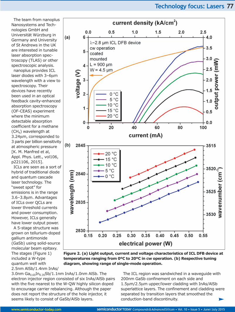
Figure 2. (a) Light output, current and voltage characteristics of ICL DFB device attemperatures ranging from 0ºC to 20ºC in cw operation. (b) Respective tuningdiagram, showing range of single-mode operation.

Broad-area, ridge-waveguide (RWG) and distributedfeedback (DFB) devices were produced from the epi-taxial material. The RWG and DFB laser diodes werepassivated with silicon nitride and silicon dioxide.For the DFB laser diodes, metal gratings on the sides
of the ridges were used for longitudinal mode selection.The top contact metals were sputtered. Electrochemicaldeposition of 10μm of gold provided thermal manage-ment. The substrate was thinned to 150μm beforedeposition of the bottom contact. The structures were cleaved into bars with 900μm
cavities. The devices were further passivated with aluminium oxide on the front facet. The back facet wascoated with a highly reflective metal mirror.The DFB devices were mounted on aluminium nitride
heat spreaders and soldered into TO packaging withthermoelectric cooling. The packaging was hermeticallysealed. The windows were anti-reflective.The broad-area laser diodes had a threshold current
density of 383A/cm2 at 20ºC under pulsed operation.According to the researchers, the threshold is onlyslightly higher than for devices with wavelengthslonger than 3μm.Cascaded type-I QW devices have been reported with
thresholds as low as 100A/cm2 for quinary diode lasersand around 300 A/cm2 for a superlattice design. QCLthresholds tend to be greater than 2kA/cm2, dependingon materials.
The characteristic tempera-ture for the threshold (T0) ofthe broad-area ICL was 67K,claimed as a record for ICLmaterial by the researchers.The emission wavelengthpeaked around 2.84μm.Narrow-RWG laser diodes
with 3mm long, 7.8μm-widecavity had continuous wave(cw) output power of morethan 11mW at 20ºC. Thesediodes emitted laser light upto 50ºC. Previous reports ofICLs with emission wave-lengths shorter than 3μmhave been for broad-areadevices in pulsed operation.The DFB output up to a few
milliwatts (less than 4mW) incw operation at room tem-perature. The threshold wasat 1.4kA/cm2. The thresholdpower was 6.2kW/cm2 —much lower than the bestindium phosphide QCLsreported so far.Current based tuning
(Figure 2) gave a 7nm wavelength range (21nm/W,0.13nm/mA). Combining current and temperature(0.29nm/K) tuning extended this to 12nm. Theresearchers say that this is more than sufficient forTLAS. By varying the DFB gratings, wavelengthsbetween 2777.5nm and 2928.8nm, a range of morethan 150nm, could be produced.
Antimony-free QWChina’s Shanghai Institute of Microsystem and Infor-mation Technology has developed a long-wavelengthindium arsenide (InAs) QW laser diode grown onindium phosphide (InP) substrate [Y. Gu et al, Appl.Phys. Lett., vol106, p121102, 2015]. The researchersclaim the longest wavelength achieved, 2.9μm, as arecord for antimony-free (Sb) structures.Antimony-based semiconductor lasers can achieve
3μm cw operation at room temperature, using gallium antimonide substrates. However, GaSb is moreexpensive than InP and presently is of lower quality.Further, GaSb-based devices suffer thermal manage-ment problems due to its low thermal conductivity. Gas-source molecular beam epitaxy (GS-MBE) was
used to grow the laser structure (Figure 3) on sulfur-doped (001) n-InP. An indium aluminium arsenidetemplate/cladding layer of 0.87μm metamorphic n-In0.8Al0.2As (485ºC) was grown on 1.6μm composi-tionally graded InAlAs buffer (495–455ºC) on top of
Technology focus: Lasers
semiconductorTODAY Compounds&AdvancedSilicon • Vol. 10 • Issue 5 • June/July 2015 www.semiconductor-today.com
78
Figure 3. Energy-band structure of InP-based metamorphic type-I QW laser.Injection directions of electrons and holes are indicated.

In0.52Al0.48As, lattice-matched with theunderlying InP substrate. The indium-content grading went from 52% to 84%,overshooting the 80% of the metamorphictemplate layer. The overshoot was designedto ensure full relaxation of the templatelayer. The n- and p-type doping for InAlAslayers were provided by silicon and beryl-lium, respectively.The active region featured a multiple QW
structure with eight 15nm InAs wells in15nm In0.6Ga0.4As barriers, grown at 435ºC.The QW material composition and thick-nesses were designed to provide straincompensation with respect to the template.The use of eight wells compensated for theimpact on radiative recombination from therelatively large density of threading disloca-tions (106–107/cm2) in the template layer. In0.8Al0.2As was chosen for the waveguide
material, which has been found to have better performance than In0.8Al0.2As orIn0.8AlyGa1–yAs alternatives. The upper p-InAlAs cladding was 1.8μm, followed by300nm p-In0.8Al0.2As for the contact. Thewaveguide, cladding and contact weregrown at 465ºC.Ridge waveguide laser diodes were pro-
duced with 8μm wide ridges. Isolation wasprovided by 300nm silicon nitride. Finisheddevices were mounted epi-side up on copper heat sinks. The measurements weremade with the devices in a liquid nitrogencryostat. A laser diode with a 0.8mm-long cavity
lased around 2.80μm at 160K under 200ns100kHz pulsed operation at 1.2x the thresh-old current. The wavelength red-shifted to2.91μm at 230K, “by far the longest wave-length of InP-based type-I QW lasers,”according to the research team.Continuous wave operation was limited to
less than 180K due to self-heating effects.The 150K cw output power was 1.2mW/facetat 400mA injection. The cw lasing operationvoltage was ~1V at 150K and ~1.2V at 180K.The pulsed and cw current density thresholds at 120K
were 812A/cm2 and 797A/cm2, respectively (Figure 4).The increase in threshold for pulsed operation had acharacteristic temperature (T0) of around 60K between120K and 200K. The corresponding figure for cw injec-tion was 53K. Above 200K, T0 for pulsed operationdecreased to 17K. This drop is attributed to increasedcarrier loss.Extrapolating the cw threshold current at 120K to
infinite cavity length gave a value of 465A/cm2. The
1.4mm cavity threshold was 650A/cm2.The researchers say that they need to improve carrier
confinement to increase operation temperatures. Electron and hole leakage could be reduced with blocking layers on the n- and p-sides of the device. The researchers describe their work as being at anearly stage. ■
The author Mike Cooke is a freelance technology journalistwho has worked in the semiconductor and advancedtechnology sectors since 1997.
Technology focus: Lasers
www.semiconductor-today.com semiconductorTODAY Compounds&AdvancedSilicon • Vol. 10 • Issue 5 • June/July 2015
79
Figure 4. Temperature dependence of threshold current densityof laser with 0.8mm cavity length under (a) pulsed and (b) cwoperation. Inset of figure (b) cw threshold current density (Jth) as a function of reciprocal cavity length (1/L) at 120K. Solid anddotted lines are fits to experimental data and extrapolation,respectively.