8-1 digital ic terminology - computer engineeringjgallaher/download/etem212/chapter8-ic...• most...
TRANSCRIPT

1
8-1 Digital IC Terminology
• Current and voltage parameters• Fan-Out• Propagation delays• Power requirements• Speed-power product• Noise immunity• Invalid voltage levels• Current-sourcing and current-sinking action• IC Packages
Ronald Tocci/Neal Widmer/Gregory MossDigital Systems: Principles and Applications, 9e
Copyright ©2004 by Pearson Education, Inc.Upper Saddle River, New Jersey 07458
All rights reserved.

2
8-2 The TTL Logic Family
• The NAND gate is the basic TTL circuit.
Ronald Tocci/Neal Widmer/Gregory MossDigital Systems: Principles and Applications, 9e
Copyright ©2004 by Pearson Education, Inc.Upper Saddle River, New Jersey 07458
All rights reserved.
3
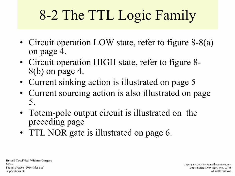
8-2 The TTL Logic Family
• Circuit operation LOW state, refer to figure 8-8(a) on page 4.
• Circuit operation HIGH state, refer to figure 8-8(b) on page 4.
• Current sinking action is illustrated on page 5• Current sourcing action is also illustrated on page
5.• Totem-pole output circuit is illustrated on the
preceding page• TTL NOR gate is illustrated on page 6.
Ronald Tocci/Neal Widmer/Gregory MossDigital Systems: Principles and Applications, 9e
Copyright ©2004 by Pearson Education, Inc.Upper Saddle River, New Jersey 07458
All rights reserved.

4
FIGURE 8-8 TTL NAND gate in its two output states.
Ronald Tocci/Neal Widmer/Gregory MossDigital Systems: Principles and Applications, 9e
Copyright ©2004 by Pearson Education, Inc.Upper Saddle River, New Jersey 07458
All rights reserved.

5
FIGURE 8-9 (a) When the TTL output is in the LOW state, Q4 acts as a current sink, deriving its current from the load. (b) In the output HIGH state, Q3 acts as a current source, providing current to the load gate.
Ronald Tocci/Neal Widmer/Gregory MossDigital Systems: Principles and Applications, 9e
Copyright ©2004 by Pearson Education, Inc.Upper Saddle River, New Jersey 07458
All rights reserved.

6
FIGURE 8-10 TTL NOR gate circuit.
Ronald Tocci/Neal Widmer/Gregory MossDigital Systems: Principles and Applications, 9e
Copyright ©2004 by Pearson Education, Inc.Upper Saddle River, New Jersey 07458
All rights reserved.

7
8-2 The TTL Logic Family
• TTL circuits have a similar structure• The input will be the cathode of a PN junction
– A HIGH input will turn off the junction and only a leakage current will flow
– A LOW input turns on the junction and a large current will flow
• Most TTL circuits have some type of totem-pole output configuration
Ronald Tocci/Neal Widmer/Gregory MossDigital Systems: Principles and Applications, 9e
Copyright ©2004 by Pearson Education, Inc.Upper Saddle River, New Jersey 07458
All rights reserved.

8
8-3 TTL Data Sheets• First line of TTL ICs was the 54/74 series
– 54 series operates over a wider temperature range• Same numbering system, prefix indicates
manufacturer– SN – Texas Instruments– DM – National Semiconductor– S – Signetics– DM7402, SN7402, S7402 all perform the same
function• Data sheets contain electrical characteristics,
switching characteristics, and recommended operating conditions.
Ronald Tocci/Neal Widmer/Gregory MossDigital Systems: Principles and Applications, 9e
Copyright ©2004 by Pearson Education, Inc.Upper Saddle River, New Jersey 07458
All rights reserved.

9
8-3 TTL Data Sheets
Ronald Tocci/Neal Widmer/Gregory MossDigital Systems: Principles and Applications, 9e
Copyright ©2004 by Pearson Education, Inc.Upper Saddle River, New Jersey 07458
All rights reserved.

10
8-3 TTL Data Sheets
• Supply voltage and temperature range• Voltage levels• Maximum voltage ratings• Power dissipation• Propagation delays
Ronald Tocci/Neal Widmer/Gregory MossDigital Systems: Principles and Applications, 9e
Copyright ©2004 by Pearson Education, Inc.Upper Saddle River, New Jersey 07458
All rights reserved.

11
8-4 TTL Series Characteristics
• Standard 74 series TTL has evolved into other series:– Standard TTL, 74 series– Schottky TTL, 74S series– Low power Schottky TTL, 74LS series (LS-TTL)– Advanced Schottky TTL, 74AS series (AS-TTL)– Advanced low power Schottky TTL, 74ALS series– 74F fast TTL
• Refer to Table 8-6 on the next page for a comparison between the series characteristics
Ronald Tocci/Neal Widmer/Gregory MossDigital Systems: Principles and Applications, 9e
Copyright ©2004 by Pearson Education, Inc.Upper Saddle River, New Jersey 07458
All rights reserved.

12
8-4 TTL Series Characteristics (Continued)
74 74S 74LS 74AS 74ALS 74F
Performance Ratings
Propagation delay (ns) 9 3 9.5 1.7 4 3
Power dissipation (mW) 10 20 2 8 1.2 6
Speed-power product (pJ) 90 60 19 13.6 4.8 18
Max. clock rate (MHz) 35 125 45 200 70 100
Fan-out (same series) 10 20 20 40 20 33
Voltage parameters
VOH(min) 2.4 2.7 2.7 2.5 2.5 2.5
VOL(max) 0.4 0.5 0.5 0.5 0.5 0.5
VIH(min) 2.0 2.0 2.0 2.0 2.0 2.0
VIL(max) 0.8 0.8 0.8 0.8 0.8 0.8
Table 8-6 Typical TTL series characteristics.

13
8-5 TTL Loading and Fan Out
• Fan out refers to the load drive capability of an IC output– A TTL output has a limit on how much current
it can sink in the LOW state– A TTL output has a limit on how much current
it can source in the HIGH state.– Exceeding these currents will result in output
voltage levels outside specified ranges
Ronald Tocci/Neal Widmer/Gregory MossDigital Systems: Principles and Applications, 9e
Copyright ©2004 by Pearson Education, Inc.Upper Saddle River, New Jersey 07458
All rights reserved.

14
FIGURE 8-13 Currents when a TTL output is driving several inputs.
Ronald Tocci/Neal Widmer/Gregory MossDigital Systems: Principles and Applications, 9e
Copyright ©2004 by Pearson Education, Inc.Upper Saddle River, New Jersey 07458
All rights reserved.

15
8-5 TTL Loading and Fan Out
• Determining fan out– Add the IIH for all inputs connected to an
output. The sum must be less than the output IOH specification.
– Add the IIL for all inputs connected to an output. The sum must be less than the output IOL specification.
Ronald Tocci/Neal Widmer/Gregory MossDigital Systems: Principles and Applications, 9e
Copyright ©2004 by Pearson Education, Inc.Upper Saddle River, New Jersey 07458
All rights reserved.
16
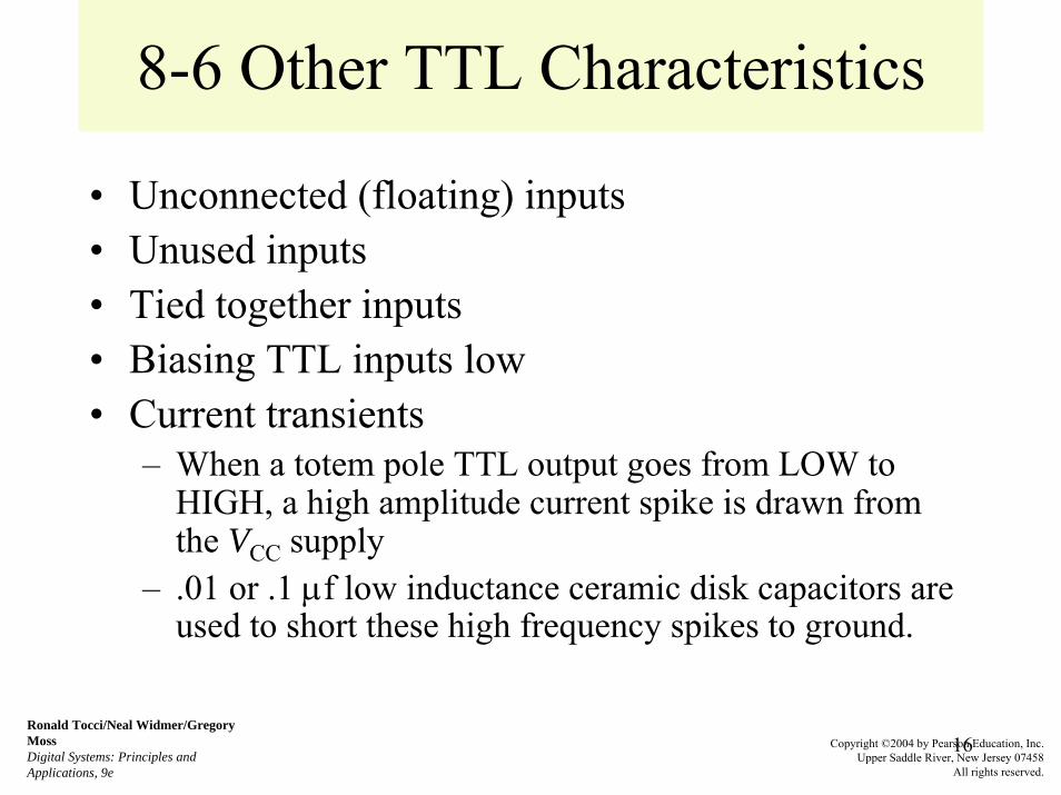
8-6 Other TTL Characteristics
• Unconnected (floating) inputs• Unused inputs• Tied together inputs• Biasing TTL inputs low• Current transients
– When a totem pole TTL output goes from LOW to HIGH, a high amplitude current spike is drawn from the VCC supply
– .01 or .1 μf low inductance ceramic disk capacitors are used to short these high frequency spikes to ground.
Ronald Tocci/Neal Widmer/Gregory MossDigital Systems: Principles and Applications, 9e
Copyright ©2004 by Pearson Education, Inc.Upper Saddle River, New Jersey 07458
All rights reserved.

17
FIGURE 8-15 Three ways to handle unused logic inputs.
Ronald Tocci/Neal Widmer/Gregory MossDigital Systems: Principles and Applications, 9e
Copyright ©2004 by Pearson Education, Inc.Upper Saddle River, New Jersey 07458
All rights reserved.

18
FIGURE 8-16 Example 8-10.
Ronald Tocci/Neal Widmer/Gregory MossDigital Systems: Principles and Applications, 9e
Copyright ©2004 by Pearson Education, Inc.Upper Saddle River, New Jersey 07458
All rights reserved.

19
FIGURE 8-17 Biasing an input low.
Ronald Tocci/Neal Widmer/Gregory MossDigital Systems: Principles and Applications, 9e
Copyright ©2004 by Pearson Education, Inc.Upper Saddle River, New Jersey 07458
All rights reserved.
20
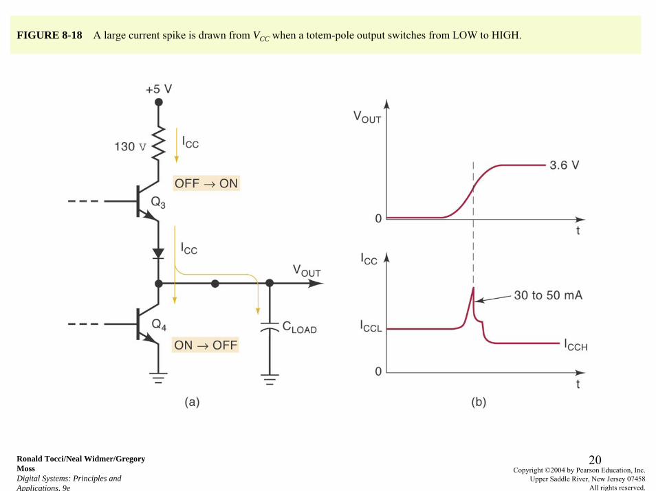
FIGURE 8-18 A large current spike is drawn from VCC when a totem-pole output switches from LOW to HIGH.
Ronald Tocci/Neal Widmer/Gregory MossDigital Systems: Principles and Applications, 9e
Copyright ©2004 by Pearson Education, Inc.Upper Saddle River, New Jersey 07458
All rights reserved.

21
8-7 MOS Technology
• Metal Oxide Semiconductor Field Effect Transistors (MOSFETs)– Simple and cheap to fabricate– Consumes very little power– More circuit elements are possible– Susceptible to static electricity damage
Ronald Tocci/Neal Widmer/Gregory MossDigital Systems: Principles and Applications, 9e
Copyright ©2004 by Pearson Education, Inc.Upper Saddle River, New Jersey 07458
All rights reserved.

22
8-7 MOS Technology
• Schematic symbols for P and N channel enhancement MOSFETs.
Ronald Tocci/Neal Widmer/Gregory MossDigital Systems: Principles and Applications, 9e
Copyright ©2004 by Pearson Education, Inc.Upper Saddle River, New Jersey 07458
All rights reserved.

23
8-7 MOS Technology (Continued)
Drain-to-Source Bias
Gate-to-Source
Voltage (VGS) Needed for Conduction
RON(Ω) ROFF(Ω)
P-channel Negative Typically more negative than -1.5v 1000 (typical) 1010
N-channel Positive Typically more positive than +1.5v 1000 (typical 1010
Table 8-8 P-channel and N-channel switching characteristics.

24
8-7 MOS Technology
• The basic MOSFET switch
Ronald Tocci/Neal Widmer/Gregory MossDigital Systems: Principles and Applications, 9e
Copyright ©2004 by Pearson Education, Inc.Upper Saddle River, New Jersey 07458
All rights reserved.

25
8-8 Digital MOSFET Circuits
• P-MOS – uses only P channel enhancement MOSFETs
• N-MOS – uses only N channel enhancement MOSFETs
• CMOS – uses both P and N channel devices
Ronald Tocci/Neal Widmer/Gregory MossDigital Systems: Principles and Applications, 9e
Copyright ©2004 by Pearson Education, Inc.Upper Saddle River, New Jersey 07458
All rights reserved.

26
FIGURE 8-21 N-MOS INVERTER.
Ronald Tocci/Neal Widmer/Gregory MossDigital Systems: Principles and Applications, 9e
Copyright ©2004 by Pearson Education, Inc.Upper Saddle River, New Jersey 07458
All rights reserved.

27
8-9 Complementary MOS Logic
• The CMOS family uses both P and N channel MOSFETs– Faster– Consumes less power– More complex fabrication
• CMOS Inverter• CMOS NAND gate• CMOS NOR gate• CMOS SET-CLEAR FF
Ronald Tocci/Neal Widmer/Gregory MossDigital Systems: Principles and Applications, 9e
Copyright ©2004 by Pearson Education, Inc.Upper Saddle River, New Jersey 07458
All rights reserved.

28
8-10 CMOS Series Characteristics
• CMOS devices compete directly with TTL– Pin compatible– Functionally equivalent– Electrically compatible
• 4000/1400 series• 74C series• 74HC/HCT (high speed CMOS)• 74AC/ACT (advanced CMOS)
Ronald Tocci/Neal Widmer/Gregory MossDigital Systems: Principles and Applications, 9e
Copyright ©2004 by Pearson Education, Inc.Upper Saddle River, New Jersey 07458
All rights reserved.

29
8-10 CMOS Series Characteristics
• 74AHC/AHCT (advanced high speed CMOS)• BiCMOS 5 volt logic (combined bipolar & CMOS)
• Power supply voltage (3-15 v)
• Logic voltage levels (VIH = higher, VIL = higher than TTL)
• Noise margins (CMOS is better than TTL)
• Power dissipation (Low)
Ronald Tocci/Neal Widmer/Gregory MossDigital Systems: Principles and Applications, 9e
Copyright ©2004 by Pearson Education, Inc.Upper Saddle River, New Jersey 07458
All rights reserved.

30
8-10 CMOS Series Characteristics
• PD increases with frequency (power supply spikes waste energy)
• Fan out (each load = 5 pf. => effects source current and propagation delay)
• Switching speed (tpd = 50 ns @ VDD = 5 and tpd = 25 @ VDD = 10 V)
• Unused inputs (tie either high or low – don’t leave un-terminated)
• Static sensitivity– ESD precautions
• Latch up (from parasitic PNP and NPN transistors embedded in the substrate)
Ronald Tocci/Neal Widmer/Gregory MossDigital Systems: Principles and Applications, 9e
Copyright ©2004 by Pearson Education, Inc.Upper Saddle River, New Jersey 07458
All rights reserved.

31
8-11 Low Voltage Technology
• CMOS family:– 74LVC (low voltage CMOS)– 74ALVC (advanced low voltage CMOS)– 74LV (low voltage)– 74AVC (advanced very low voltage CMOS)– 74AUC (advanced ultra-low voltage CMOS)– 74CBT (cross bar technology)– 74CBTLV (cross bar technology low voltage)– 74GTLP1394 (gunning transceivers logic plus)– 74SSTV (stub series terminated logic)– 74TVC (translation voltage clamp)
Ronald Tocci/Neal Widmer/Gregory MossDigital Systems: Principles and Applications, 9e
Copyright ©2004 by Pearson Education, Inc.Upper Saddle River, New Jersey 07458
All rights reserved.

32
8-11 Low Voltage Technology
• BiCMOS family:– 74LVT (low voltage BiCMOS technology)– 74ALVT (advanced low voltage BiCMOS technology)– 74ALB (advanced low voltage BiCMOS)
• The move toward low voltage systems will continue and the technician must be prepared to operate in an environment where devices may not necessarily operate on 5 volts.
Ronald Tocci/Neal Widmer/Gregory MossDigital Systems: Principles and Applications, 9e
Copyright ©2004 by Pearson Education, Inc.Upper Saddle River, New Jersey 07458
All rights reserved.

33
FIGURE 8-27 Logic product life cycle. (Courtesy of Texas Instruments)
Ronald Tocci/Neal Widmer/Gregory MossDigital Systems: Principles and Applications, 9e
Copyright ©2004 by Pearson Education, Inc.Upper Saddle River, New Jersey 07458
All rights reserved.

34
8-12 Open Collector/Open Drain Outputs
• Conventional CMOS outputs and TTL totem pole outputs should never be connected to the same point.
Ronald Tocci/Neal Widmer/Gregory MossDigital Systems: Principles and Applications, 9e
Copyright ©2004 by Pearson Education, Inc.Upper Saddle River, New Jersey 07458
All rights reserved.

35
8-12 Open Collector/Open Drain Outputs
• Open-collector/open-drain outputs
Wired-AND with open collectors

36
8-12 Open Collector/Open Drain Outputs
• Open-collector/open-drain buffer/drivers

37
8-13 Tristate (Three-State) Logic Outputs
• Three states are possible: HIGH, LOW, and high impedance.
• Advantages of tristate devices:– Share bus– No sacrifice of speed
Ronald Tocci/Neal Widmer/Gregory MossDigital Systems: Principles and Applications, 9e
Copyright ©2004 by Pearson Education, Inc.Upper Saddle River, New Jersey 07458
All rights reserved.

38
8-13 Tristate (Three-State) Logic Outputs
• Tristate buffers
• Tristate ICs (flip-flops, and other bus oriented devices)

39
8-14 High-Speed Bus Interface Logic
• At high frequencies bus wires of more than about 4 inches in length act like transmission lines.
• In order to prevent reflected waves, the end of a bus must be terminated with a resistance equal to the line impedance (about 50 Ohms).
• Figure 8-40 on the next page describes termination techniques.
Ronald Tocci/Neal Widmer/Gregory MossDigital Systems: Principles and Applications, 9e
Copyright ©2004 by Pearson Education, Inc.Upper Saddle River, New Jersey 07458
All rights reserved.

40
FIGURE 8-40 Bus termination techniques.
Ronald Tocci/Neal Widmer/Gregory MossDigital Systems: Principles and Applications, 9e
Copyright ©2004 by Pearson Education, Inc.Upper Saddle River, New Jersey 07458
All rights reserved.

41
8-15 The ECL Digital IC Family• Emitter coupled logic – increases switching speed.• Basic ECL circuit
Ronald Tocci/Neal Widmer/Gregory MossDigital Systems: Principles and Applications, 9e
Copyright ©2004 by Pearson Education, Inc.Upper Saddle River, New Jersey 07458
All rights reserved.
Basic ECL Circuit with Operating States Emitter-Follower Stages for Level Shifting

42
8-15 The ECL Digital IC Family
• ECL OR/NOR gate

43
8-15 The ECL Digital IC Family
• ECL characteristics– Very fast switching, typical propagation delay is 360 ps– -0.8 V logic 1, -1.7 V logic 0– Noise margins approximately 150 mV– Output complement is produced, eliminating need for
inverters– Typical fan out is 25– Typical power dissipation is 25 mW– Current flow remains constant, eliminating noise spikes
44
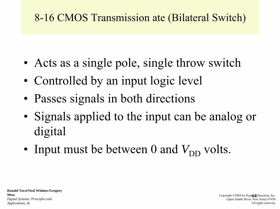
8-16 CMOS Transmission ate (Bilateral Switch)
• Acts as a single pole, single throw switch• Controlled by an input logic level• Passes signals in both directions• Signals applied to the input can be analog or
digital• Input must be between 0 and VDD volts.
Ronald Tocci/Neal Widmer/Gregory MossDigital Systems: Principles and Applications, 9e
Copyright ©2004 by Pearson Education, Inc.Upper Saddle River, New Jersey 07458
All rights reserved.

45
FIGURE 8-43 CMOS bilateral switch (transmission gate).
Ronald Tocci/Neal Widmer/Gregory MossDigital Systems: Principles and Applications, 9e
Copyright ©2004 by Pearson Education, Inc.Upper Saddle River, New Jersey 07458
All rights reserved.

46
FIGURE 8-45 Example 8-12: 74HC4016 bilateral switches used to switch an analog signal to two different outputs.
Ronald Tocci/Neal Widmer/Gregory MossDigital Systems: Principles and Applications, 9e
Copyright ©2004 by Pearson Education, Inc.Upper Saddle River, New Jersey 07458
All rights reserved.

47
8-17 IC Interfacing
• Driver – provides the output signal.• Load – receives the signal.• Interface circuit – connected between driver
and load to condition the signal for the load.• Interfacing between logic families is
common in digital systems.• Table 8-12 on the next page summarizes
current parameters for standard devices.
Ronald Tocci/Neal Widmer/Gregory MossDigital Systems: Principles and Applications, 9e
Copyright ©2004 by Pearson Education, Inc.Upper Saddle River, New Jersey 07458
All rights reserved.

48
8-17 IC Interfacing
CMOSParameter 4000B 74HC/HCT 74AC/ACT 74AHC/AHCTIIH(max) 1 uA 1 uA 1 uA 1 uAIIL(max) 1 uA 1 uA 1 uA 1 uAIOH(max) 0.4 mA 4 mA 24 mA 8 mAIOL(max) 0.4 mA 4 mA 24 mA 8 mA
TTL
8 mA4.0 mA100 uA20 uA74ALS
20 mA20 mA8 mA16 mAIOL(max)1.0 mA2 mA4 mA0.4 mAIOH(max)0.6 mA0.5 mA0.4 mA1.6 mAIIL(max)20 uA20 uA20 uA40 uAIIH(max)74F74AS74LS74Parameter

49
8-18 TTL Driving CMOS
• TTL easily meets CMOS input current requirements• TTL output voltage must be raised for input to some
CMOS devices. The most common solution is a pull-up resistor.
• TTL driving high voltage CMOS
Ronald Tocci/Neal Widmer/Gregory MossDigital Systems: Principles and Applications, 9e
Copyright ©2004 by Pearson Education, Inc.Upper Saddle River, New Jersey 07458
All rights reserved.

50
8-19 CMOS Driving TTL
• CMOS output for both logic states• CMOS driving TTL in the HIGH state• CMOS driving TTL in the LOW state
Ronald Tocci/Neal Widmer/Gregory MossDigital Systems: Principles and Applications, 9e
Copyright ©2004 by Pearson Education, Inc.Upper Saddle River, New Jersey 07458
All rights reserved.

51
8-19 CMOS Driving TTL
• High voltage CMOS driving TTL
4058 buffer acts as level translator

52
8-20 Analog Voltage Comparators
• Useful in systems with analog and digital components• Compares two voltages. If voltage on the (+) input is
greater than (-) input the output is high. If input on the (-) is greater the output is low.
• May be considered a one bit analog to digital converter.• The LM339 IC
Ronald Tocci/Neal Widmer/Gregory MossDigital Systems: Principles and Applications, 9e
Copyright ©2004 by Pearson Education, Inc.Upper Saddle River, New Jersey 07458
All rights reserved.

53
8-21 Troubleshooting
• Logic pulser – tool that generates a short pulse when actuated– Senses the existing voltage level and produces a
pulse in the opposite polarity– Output impedance of 2 Ohms or less
• Using logic pulser and probe to test a circuit• Finding shorted nodes
Ronald Tocci/Neal Widmer/Gregory MossDigital Systems: Principles and Applications, 9e
Copyright ©2004 by Pearson Education, Inc.Upper Saddle River, New Jersey 07458
All rights reserved.

54
FIGURE 8-53 A logic pulser can inject a pulse at any node that is not shorted directly to ground or VCC.
Ronald Tocci/Neal Widmer/Gregory MossDigital Systems: Principles and Applications, 9e
Copyright ©2004 by Pearson Education, Inc.Upper Saddle River, New Jersey 07458
All rights reserved.

55
FIGURE 8-54 A logic pulser and a logic probe can be used to trace shorted nodes.
Ronald Tocci/Neal Widmer/Gregory MossDigital Systems: Principles and Applications, 9e
Copyright ©2004 by Pearson Education, Inc.Upper Saddle River, New Jersey 07458
All rights reserved.