8-channel differential das with 18-bit, bipolar
TRANSCRIPT
8-Channel Differential DAS with 18-Bit, Bipolar, Simultaneous Sampling ADC
Data Sheet AD7609
FEATURES 8 simultaneously sampled inputs True differential inputs True bipolar analog input ranges: ±10 V, ±5 V Single 5 V analog supply and 2.3 V to 5.25 V VDRIVE Fully integrated data acquisition solution
Analog input clamp protection Input buffer with 1 MΩ analog input impedance Second-order antialiasing analog filter On-chip accurate reference and reference buffer 18-bit ADC with 200 kSPS on all channels Oversampling capability with digital filter
Flexible parallel/serial interface SPI/QSPI™/MICROWIRE™/DSP compatible Performance
7 kV ESD rating on analog input channels 98 dB SNR, −107 dB THD Dynamic range: up to 105 dB typical Low power: 100 mW Standby mode: 25 mW
64-lead LQFP package
APPLICATIONS Power line monitoring and protection systems Multiphase motor control Instrumentation and control systems Multiaxis positioning systems Data acquisition systems (DAS)
COMPANION PRODUCTS External References: ADR421, ADR431 Digital Isolators: ADuM1402, ADuM5000, ADuM5402 Power: ADIsimPower, Supervisor Parametric Search Additional companion products on the AD7609 product page
Table 1. High Resolution, Bipolar Input, Simultaneous Sampling DAS Solutions
Resolution
Single-Ended Inputs
True Differential Inputs
Number of Simultaneous Sampling Channels
18 Bits AD7608 AD76091 8 16 Bits AD7606 8 AD7606-6 6 AD7606-4 4 14 Bits AD7607 8
1 Protected by U.S. Patent Number 8,072,360 B2.
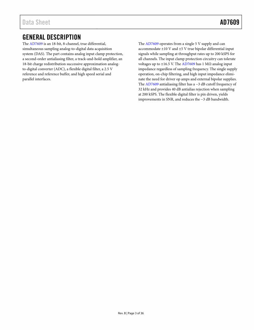
FUNCTIONAL BLOCK DIAGRAM
V1+V1–
RFB
RFB
RFB
RFB
RFB
RFB
RFB
RFB
RFB
RFB
RFB
RFB
RFB
RFB
RFB
RFB
1MΩ
1MΩ
CLAMPCLAMP
T/H
V2+V2–
1MΩ
1MΩ
CLAMPCLAMP
T/H
V3+V3–
1MΩ
1MΩ
CLAMPCLAMP
T/H
V4+V4–
1MΩ
1MΩ
CLAMPCLAMP
T/H
V5+V5–
1MΩ
1MΩ
CLAMPCLAMP
T/H
V6+V6–
1MΩ
1MΩ
CLAMPCLAMP
T/H
V7+V7–
1MΩ
1MΩ
CLAMPCLAMP
T/H
V8+V8–
1MΩ
1MΩ
CLAMPCLAMP
T/H
8:1MUX
AGND
BUSYFRSTDATA
CONVST A CONVST B RESET RANGE
CONTROLINPUTS
CLK OSC
REFIN/REFOUT
REF SELECT
AGND
OS 2OS 1OS 0
DOUTADOUTB
RD/SCLKCS
PAR/SER SELVDRIVE
18-BITSAR
DIGITALFILTER
PARALLEL/SERIAL
INTERFACE
2.5VREF
REFCAPB REFCAPA
SERIAL
PARALLEL
REGCAP
2.5VLDO
REGCAP
2.5VLDO
AVCCAVCC
DB[15:0]
AD7609
0976
0-00
1SECOND-
ORDER LPF
SECOND-ORDER LPF
SECOND-ORDER LPF
SECOND-ORDER LPF
SECOND-ORDER LPF
SECOND-ORDER LPF
SECOND-ORDER LPF
SECOND-ORDER LPF
Figure 1.
Rev. B Document Feedback Information furnished by Analog Devices is believed to be accurate and reliable. However, no responsibility is assumed by Analog Devices for its use, nor for any infringements of patents or other rights of third parties that may result from its use. Specifications subject to change without notice. No license is granted by implication or otherwise under any patent or patent rights of Analog Devices. Trademarks and registered trademarks are the property of their respective owners.
One Technology Way, P.O. Box 9106, Norwood, MA 02062-9106, U.S.A. Tel: 781.329.4700 ©2011–2014 Analog Devices, Inc. All rights reserved. Technical Support www.analog.com

AD7609 Data Sheet
TABLE OF CONTENTS Features .............................................................................................. 1 Applications ....................................................................................... 1 Companion Products ....................................................................... 1 Functional Block Diagram .............................................................. 1 Revision History ............................................................................... 2 General Description ......................................................................... 3 Specifications ..................................................................................... 4
Timing Specifications .................................................................. 7 Absolute Maximum Ratings .......................................................... 11
Thermal Resistance .................................................................... 11 ESD Caution ................................................................................ 11
Pin Configuration and Function Descriptions ........................... 12 Typical Performance Characteristics ........................................... 15 Terminology .................................................................................... 19 Theory of Operation ...................................................................... 21
Converter Details ....................................................................... 21 Analog Input ............................................................................... 21 ADC Transfer Function ............................................................. 22 Internal/External Reference ...................................................... 23 Typical Connection Diagram ................................................... 24 Power-Down Modes .................................................................. 24 Conversion Control ................................................................... 25
Digital Interface .............................................................................. 26 Parallel Interface (PAR/SER SEL = 0) ...................................... 26 Serial Interface (PAR/SER SEL = 1) ......................................... 26 Reading During Conversion ..................................................... 27 Digital Filter ................................................................................ 28 Layout Guidelines....................................................................... 32
Outline Dimensions ....................................................................... 34 Ordering Guide .......................................................................... 34
REVISION HISTORY 5/14—Rev. A to Rev. B
Changes to Patent Footnote ............................................................. 1 Changes to Figure 37 ....................................................................... 22 Changes to Figure 39 and Figure 40 .............................................. 23 2/12—Rev. 0 to Rev. A Changes to Analog Input Ranges Section .................................... 21
7/11—Revision 0: Initial Version
Rev. B | Page 2 of 36
Data Sheet AD7609
GENERAL DESCRIPTION The AD7609 is an 18-bit, 8-channel, true differential, simultaneous sampling analog-to-digital data acquisition system (DAS). The part contains analog input clamp protection, a second-order antialiasing filter, a track-and-hold amplifier, an 18-bit charge redistribution successive approximation analog-to-digital converter (ADC), a flexible digital filter, a 2.5 V reference and reference buffer, and high speed serial and parallel interfaces.
The AD7609 operates from a single 5 V supply and can accommodate ±10 V and ±5 V true bipolar differential input signals while sampling at throughput rates up to 200 kSPS for all channels. The input clamp protection circuitry can tolerate voltages up to ±16.5 V. The AD7609 has 1 MΩ analog input impedance regardless of sampling frequency. The single supply operation, on-chip filtering, and high input impedance elimi-nate the need for driver op amps and external bipolar supplies. The AD7609 antialiasing filter has a −3 dB cutoff frequency of 32 kHz and provides 40 dB antialias rejection when sampling at 200 kSPS. The flexible digital filter is pin driven, yields improvements in SNR, and reduces the −3 dB bandwidth.
Rev. B | Page 3 of 36
AD7609 Data Sheet
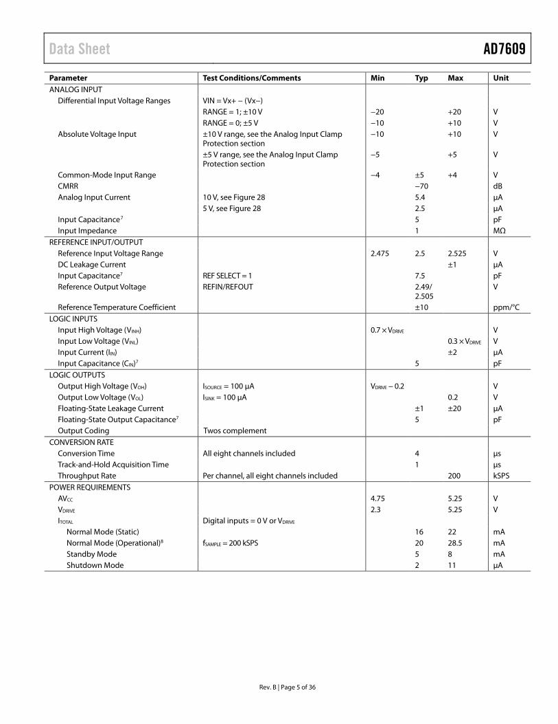
SPECIFICATIONS VREF = 2.5 V external/internal, AVCC = 4.75 V to 5.25 V, VDRIVE = 2.3 V to 5.25 V; fSAMPLE = 200 kSPS, TA = TMIN to TMAX, unless otherwise noted.1
Table 2. Parameter Test Conditions/Comments Min Typ Max Unit DYNAMIC PERFORMANCE fIN = 1 kHz sine wave unless otherwise noted
Signal-to-Noise Ratio (SNR)2, 3 Oversampling by 16; ±10 V range; fIN = 160 Hz 98 101 dB Oversampling by 16; ±5 V range; fIN = 160 Hz 100 dB No oversampling; ±10 V range 90 91 dB No oversampling; ±5 V range 89.5 90.5 dB Signal-to-(Noise + Distortion) (SINAD)2 No oversampling; ±10 V range 89.5 91 dB No oversampling; ±5 V range 89 90 dB Dynamic Range No oversampling; ±10 V range 91.5 dB No oversampling; ±5 V range 90.5 dB Total Harmonic Distortion (THD)2, 3 No oversampling; ±10 V range −107 −97 dB No oversampling; ±5 V range −110 −96 dB Peak Harmonic or Spurious Noise (SFDR)2 −108 dB Intermodulation Distortion (IMD)2 fa = 1 kHz, fb = 1.1 kHz
Second-Order Terms −110 dB Third-Order Terms −106 dB
Channel-to-Channel Isolation2 fIN on unselected channels up to 160 kHz −95 dB ANALOG INPUT FILTER
Full Power Bandwidth −3 dB, ±10 V range 32 kHz −3 dB, ±5 V range 23 kHz −0.1 dB, ±10 V range 13 kHz −0.1 dB, ±5 V range 10 kHz tGROUP DELAY ±10 V range 7.1 µs ±5 V range 10.2 µs
DC ACCURACY Resolution No missing codes 18 Bits Differential Nonlinearity2 ±0.75 −0.99/+2 LSB4 Integral Nonlinearity2 ±3 ±7.5 LSB Total Unadjusted Error (TUE) ±10 V range ±10 LSB ±5 V range ±90 LSB Positive Full-Scale Error2, 5 External reference ±8 ±140 LSB Internal reference ±40 LSB Positive Full-Scale Error Drift External reference ±2 ppm/°C Internal reference ±7 ppm/°C Positive Full-Scale Error Matching2 ±10 V range 12 80 LSB ±5 V range 40 100 LSB Bipolar Zero Code Error2, 6 ±10 V range ±3 ±24 LSB ± 5 V range ±3 ±48 LSB Bipolar Zero Code Error Drift ±10 V range 10 µV/°C ± 5 V range 5 µV/°C Bipolar Zero Code Error Matching2 ±10 V range 2.7 30 LSB ±5 V range 13 65 LSB Negative Full-Scale Error2, 5 External reference ±8 ±140 LSB Internal reference ±40 LSB Negative Full-Scale Error Drift External reference ±4 ppm/°C Internal reference ±8 ppm/°C Negative Full-Scale Error Matching2 ±10 V range 12 80 LSB ±5 V range 40 100 LSB
Rev. B | Page 4 of 36
Data Sheet AD7609
Parameter Test Conditions/Comments Min Typ Max Unit ANALOG INPUT
Differential Input Voltage Ranges VIN = Vx+ − (Vx−) RANGE = 1; ±10 V −20 +20 V RANGE = 0; ±5 V −10 +10 V Absolute Voltage Input ±10 V range, see the Analog Input Clamp
Protection section −10 +10 V
±5 V range, see the Analog Input Clamp Protection section
−5 +5 V
Common-Mode Input Range −4 ±5 +4 V CMRR −70 dB Analog Input Current 10 V, see Figure 28 5.4 µA 5 V, see Figure 28 2.5 µA Input Capacitance7 5 pF Input Impedance 1 MΩ
REFERENCE INPUT/OUTPUT Reference Input Voltage Range 2.475 2.5 2.525 V DC Leakage Current ±1 µA Input Capacitance7 REF SELECT = 1 7.5 pF Reference Output Voltage REFIN/REFOUT 2.49/
2.505 V
Reference Temperature Coefficient ±10 ppm/°C LOGIC INPUTS
Input High Voltage (VINH) 0.7 × VDRIVE V Input Low Voltage (VINL) 0.3 × VDRIVE V Input Current (IIN) ±2 µA Input Capacitance (CIN)7 5 pF
LOGIC OUTPUTS Output High Voltage (VOH) ISOURCE = 100 µA VDRIVE − 0.2 V Output Low Voltage (VOL) ISINK = 100 µA 0.2 V Floating-State Leakage Current ±1 ±20 µA Floating-State Output Capacitance7 5 pF Output Coding Twos complement
CONVERSION RATE Conversion Time All eight channels included 4 µs Track-and-Hold Acquisition Time 1 µs Throughput Rate Per channel, all eight channels included 200 kSPS
POWER REQUIREMENTS AVCC 4.75 5.25 V VDRIVE 2.3 5.25 V ITOTAL Digital inputs = 0 V or VDRIVE
Normal Mode (Static) 16 22 mA Normal Mode (Operational)8 fSAMPLE = 200 kSPS 20 28.5 mA Standby Mode 5 8 mA Shutdown Mode 2 11 µA
Rev. B | Page 5 of 36
AD7609 Data Sheet
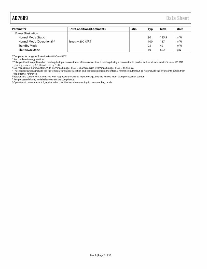
Parameter Test Conditions/Comments Min Typ Max Unit Power Dissipation
Normal Mode (Static) 80 115.5 mW Normal Mode (Operational)8 fSAMPLE = 200 kSPS 100 157 mW Standby Mode 25 42 mW Shutdown Mode 10 60.5 µW
1 Temperature range for B version is −40°C to +85°C. 2 See the Terminology section. 3 This specification applies when reading during a conversion or after a conversion. If reading during a conversion in parallel and serial modes with VDRIVE = 5 V, SNR
typically reduces by 1.5 dB and THD by 3 dB. 4 LSB means least significant bit. With ±5 V input range, 1 LSB = 76.29 µV. With ±10 V input range, 1 LSB = 152.58 µV. 5 These specifications include the full temperature range variation and contribution from the internal reference buffer but do not include the error contribution from
the external reference. 6 Bipolar zero code error is calculated with respect to the analog input voltage. See the Analog Input Clamp Protection section. 7 Sample tested during initial release to ensure compliance. 8 Operational power/current figure includes contribution when running in oversampling mode.
Rev. B | Page 6 of 36

Data Sheet AD7609
TIMING SPECIFICATIONS AVCC = 4.75 V to 5.25 V, VDRIVE = 2.3 V to 5.25 V, VREF = 2.5 V external reference/ internal reference, TA = TMIN to TMAX, unless otherwise noted.1
Table 3. Limit at TMIN, TMAX Parameter Min Typ Max Unit Description PARALLEL/SERIAL/BYTE MODE
tCYCLE 1/throughput rate 5 µs Parallel mode, reading during; or after conversion VDRIVE = 2.7 V to 5.25 V; or
serial mode: VDRIVE = 3.3 V to 5.25 V, reading during a conversion using DOUTA and DOUTB lines
5 µs Parallel mode reading after conversion VDRIVE = 2.3 V 10.1 µs Serial mode reading after conversion; VDRIVE = 2.7 V, DOUTA and DOUTB lines 11.5 µs Serial mode reading after a conversion; VDRIVE = 2.3 V, DOUTA and DOUTB lines tCONV Conversion time 3.45 4 4.15 µs Oversampling off 7.87 9.1 µs Oversampling by 2 16.05 18.8 µs Oversampling by 4 33 39 µs Oversampling by 8 66 78 µs Oversampling by 16 133 158 µs Oversampling by 32 257 315 µs Oversampling by 64 tWAKE-UP STANDBY 100 µs STBY rising edge to CONVST x rising edge; power-up time from standby mode
tWAKE-UP SHUTDOWN Internal Reference 30 ms STBY rising edge to CONVST x rising edge; power-up time from
shutdown mode External Reference 13 ms STBY rising edge to CONVST x rising edge; power-up time from
shutdown mode tRESET 50 ns RESET high pulse width tOS_SETUP 20 ns BUSY to OS x pin setup time tOS_HOLD 20 ns BUSY to OS x pin hold time t1 45 ns CONVST x high to BUSY high t2 25 ns Minimum CONVST x low pulse t3 25 ns Minimum CONVST x high pulse t4 0 ns BUSY falling edge to CS falling edge setup time
t52 0.5 ms Maximum delay allowed between CONVST A, CONVST B rising edges
t6 25 ns Maximum time between last CS rising edge and BUSY falling edge
t7 25 ns Minimum delay between RESET low to CONVST x high PARALLEL READ OPERATION
t8 0 ns CS to RD setup time
t9 0 ns CS to RD hold time
t10 RD low pulse width
19 ns VDRIVE above 4.75 V 24 ns VDRIVE above 3.3 V 30 ns VDRIVE above 2.7 V 37 ns VDRIVE above 2.3 V t11 15 ns RD high pulse width
t12 22 ns CS high pulse width (see Figure 5); CS and RD linked
Rev. B | Page 7 of 36
AD7609 Data Sheet
Limit at TMIN, TMAX Parameter Min Typ Max Unit Description
t13 Delay from CS until DB[15:0] three-state disabled
19 ns VDRIVE above 4.75 V 24 ns VDRIVE above 3.3 V 30 ns VDRIVE above 2.7 V 37 ns VDRIVE above 2.3 V t14
3 Data access time after RD falling edge
19 ns VDRIVE above 4.75 V 24 ns VDRIVE above 3.3 V 30 ns VDRIVE above 2.7 V 37 ns VDRIVE above 2.3 V t15 6 ns Data hold time after RD falling edge
t16 6 ns CS to DB[15:0] hold time
t17 22 ns Delay from CS rising edge to DB[15:0] three-state enabled
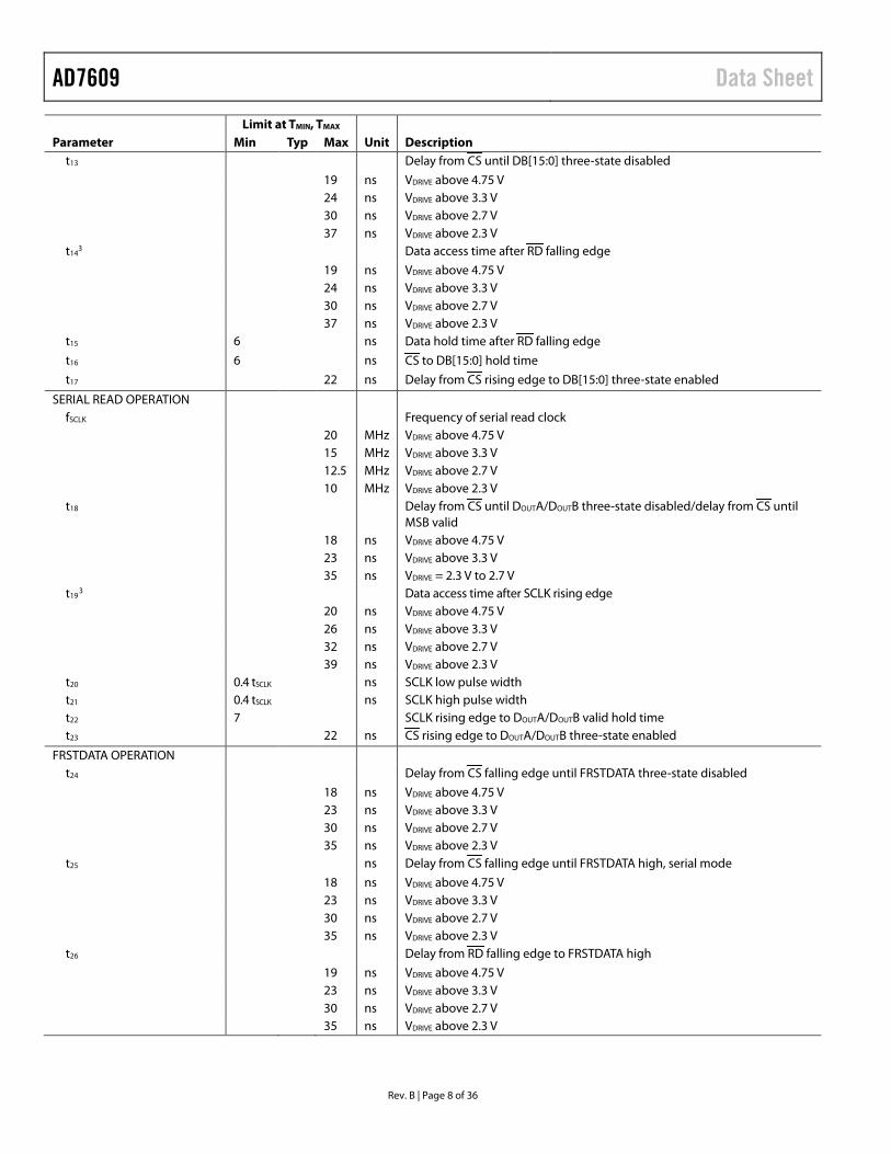
SERIAL READ OPERATION fSCLK Frequency of serial read clock 20 MHz VDRIVE above 4.75 V 15 MHz VDRIVE above 3.3 V 12.5 MHz VDRIVE above 2.7 V 10 MHz VDRIVE above 2.3 V t18 Delay from CS until DOUTA/DOUTB three-state disabled/delay from CS until
MSB valid 18 ns VDRIVE above 4.75 V 23 ns VDRIVE above 3.3 V 35 ns VDRIVE = 2.3 V to 2.7 V t19
3 Data access time after SCLK rising edge 20 ns VDRIVE above 4.75 V 26 ns VDRIVE above 3.3 V 32 ns VDRIVE above 2.7 V 39 ns VDRIVE above 2.3 V t20 0.4 tSCLK ns SCLK low pulse width t21 0.4 tSCLK ns SCLK high pulse width t22 7 SCLK rising edge to DOUTA/DOUTB valid hold time t23 22 ns CS rising edge to DOUTA/DOUTB three-state enabled
FRSTDATA OPERATION t24 Delay from CS falling edge until FRSTDATA three-state disabled
18 ns VDRIVE above 4.75 V 23 ns VDRIVE above 3.3 V 30 ns VDRIVE above 2.7 V 35 ns VDRIVE above 2.3 V t25 ns Delay from CS falling edge until FRSTDATA high, serial mode
18 ns VDRIVE above 4.75 V 23 ns VDRIVE above 3.3 V 30 ns VDRIVE above 2.7 V 35 ns VDRIVE above 2.3 V t26 Delay from RD falling edge to FRSTDATA high
19 ns VDRIVE above 4.75 V 23 ns VDRIVE above 3.3 V 30 ns VDRIVE above 2.7 V 35 ns VDRIVE above 2.3 V
Rev. B | Page 8 of 36

Data Sheet AD7609
Limit at TMIN, TMAX Parameter Min Typ Max Unit Description
t27 Delay from RD falling edge to FRSTDATA low
22 ns VDRIVE = 3.3 V to 5.25 V 29 ns VDRIVE = 2.3 V to 2.7 V t28 Delay from 18th SCLK falling edge to FRSTDATA low 20 ns VDRIVE = 3.3 V to 5.25 V 27 ns VDRIVE = 2.3 V to 2.7 V t29 29 ns Delay from CS rising edge until FRSTDATA three-state enabled
1 Sample tested during initial release to ensure compliance. All input signals are specified with tR = tF = 5 ns (30% to 70% of VDD) and timed from a voltage level of 1.6 V. 2 The delay between the CONVST x signals was measured as the maximum time allowed while ensuring a <40 LSB performance matching between channel sets. 3 A buffer is used on the data output pins for these measurements, which is equivalent to a load of 20 pF on the output pins.
Timing Diagrams
tCYCLE
t3
t5
t2
t4
t1
t7tRESET
tCONV
CONVST A/CONVST B
CONVST A/CONVST B
BUSY
CS
RESET
0976
0-00
2
Figure 2. CONVST x Timing—Reading After a Conversion
tCYCLE
t3
t5
t6
t2
t1
tCONV
CONVST A/CONVST B
CONVST A/CONVST B
BUSY
CS t7
tRESETRESET
0976
0-00
3
Figure 3. CONVST x Timing—Reading During a Conversion
DATA:DB[15:0]
FRSTDATA
CS
RD
INVALIDV1
[17:2]V1
[1:0]V2
[17:2]V8
[17:2]V8
[1:0]V2
[1:0]
t10t8
t13
t24t26 t27
t14
t11t9
t16
t17
t29
t15
0976
0-00
4
Figure 4. Parallel Mode Separate CS and RD Pulses
Rev. B | Page 9 of 36
AD7609 Data Sheet
DATA:DB[15:0]
FRSTDATA
CS, RD
V1[17:2]
V1[1:0]
V2[17:2]
V2[1:0]
V7[17:2]
V7[1:0]
V8[17:2]
V8[1:0]
t12
t13 t16 t17
0976
0-00
5
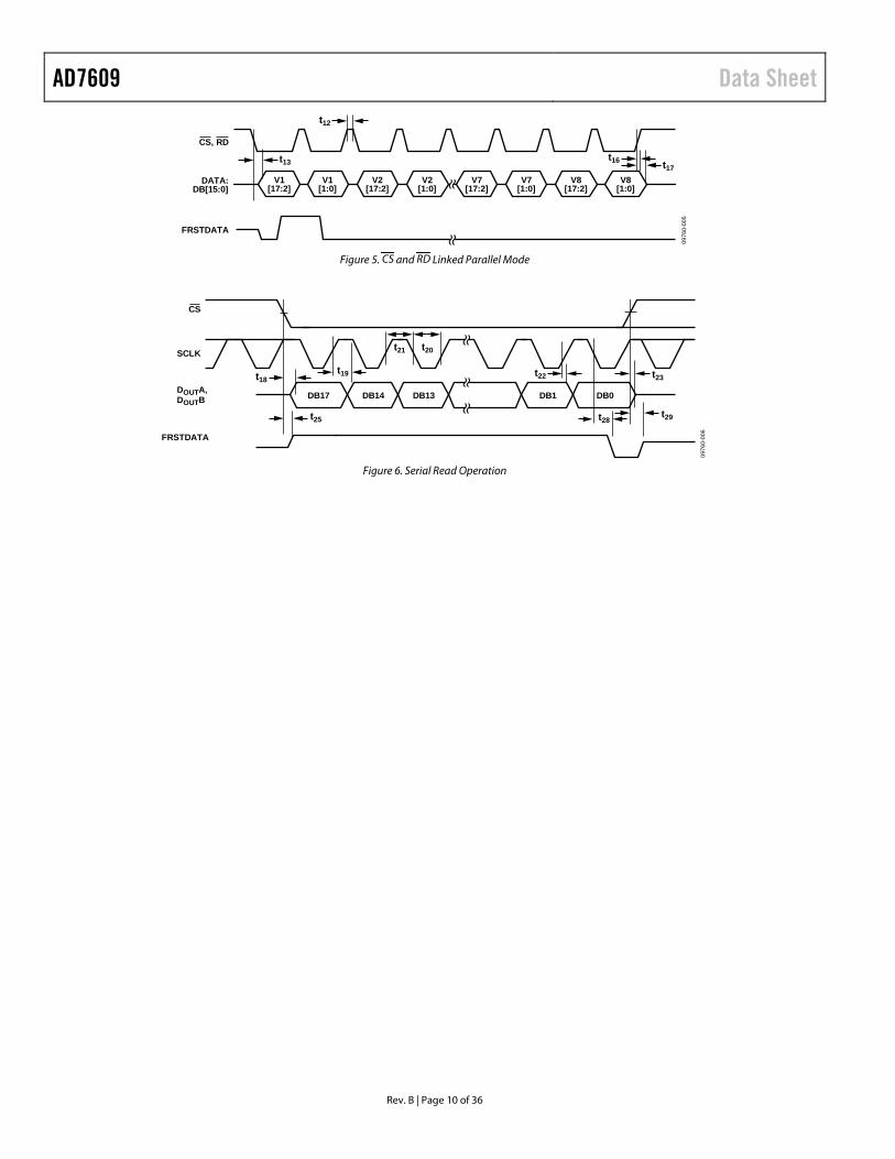
Figure 5. CS and RD Linked Parallel Mode
SCLK
DOUTA,DOUTB
FRSTDATA
CS
DB17 DB14 DB13 DB1 DB0
t18t19
t21 t20
t23
t29t28t25
t22
0976
0-00
6
Figure 6. Serial Read Operation
Rev. B | Page 10 of 36

Data Sheet AD7609
ABSOLUTE MAXIMUM RATINGS TA = 25°C, unless otherwise noted.
Table 4. Parameter Rating AVCC to AGND −0.3 V to +7 V VDRIVE to AGND −0.3 V to AVCC + 0.3 V Analog Input Voltage to AGND1 ±16.5 V Digital Input Voltage to AGND −0.3 V to VDRIVE + 0.3 V Digital Output Voltage to AGND −0.3 V to VDRIVE + 0.3 V REFIN to AGND −0.3 V to AVCC + 0.3 V Input Current to Any Pin Except
Supplies1 ±10 mA
Operating Temperature Range B Version −40°C to +85°C
Storage Temperature Range −65°C to +150°C Junction Temperature 150°C Pb/SN Temperature, Soldering
Reflow (10 sec to 30 sec) 240(+0)°C Pb-Free Temperature, Soldering Reflow 260(+0)°C ESD (All Pins Except Analog Inputs) 2 kV ESD (Analog Input Pins Only) 7 kV
1 Transient currents of up to 100 mA do not cause SCR latch-up.
Stresses above those listed under Absolute Maximum Ratings may cause permanent damage to the device. This is a stress rating only; functional operation of the device at these or any other conditions above those indicated in the operational section of this specification is not implied. Exposure to absolute maximum rating conditions for extended periods may affect device reliability.
THERMAL RESISTANCE θJA is specified for the worst-case conditions, that is, a device soldered in a circuit board for surface-mount packages. These specifications apply to a 4-layer board.
Table 5. Thermal Resistance Package Type θJA θJC Unit 64-Lead LQFP 45 11 °C/W
ESD CAUTION
Rev. B | Page 11 of 36
AD7609 Data Sheet
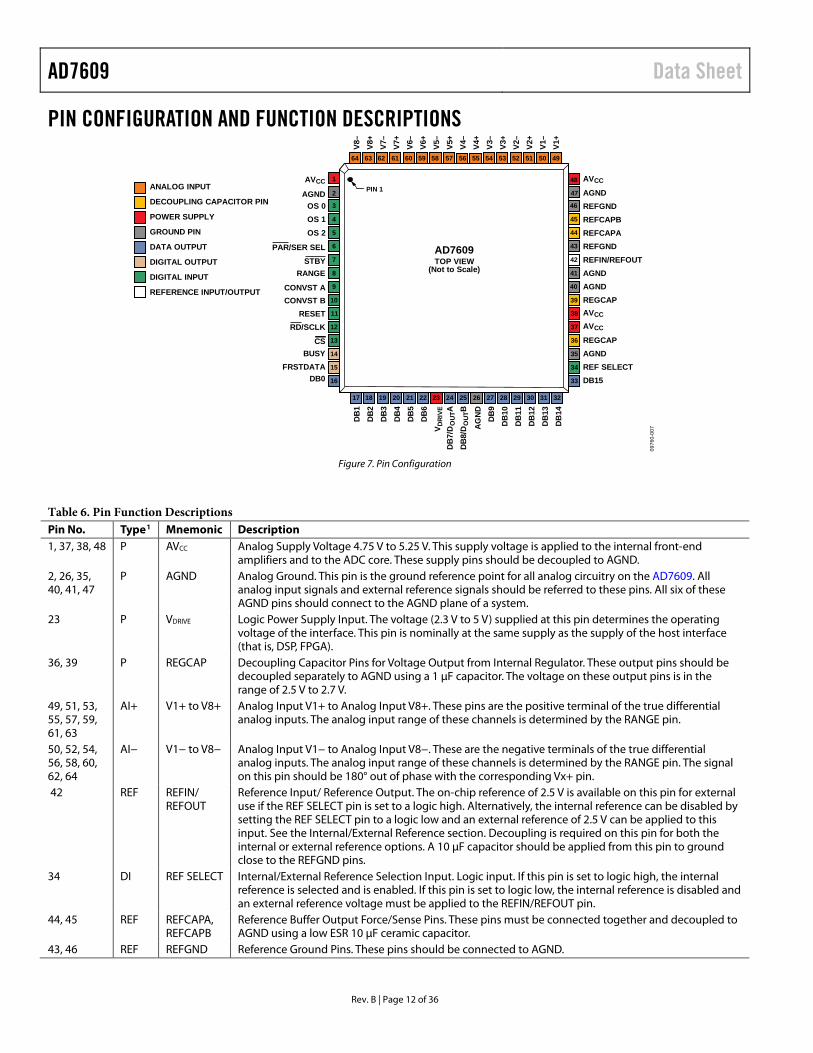
PIN CONFIGURATION AND FUNCTION DESCRIPTIONS
AD7609TOP VIEW
(Not to Scale)
64 63 62 61 60 59 58 57
V1–
56 55 54 53 52 51 50 49
V5+
V4+
V6+
V3+
V2+
V1+
PIN 1
V7+
V8+
V2–
V3–
V4–
V5–
V6–
V7–
V8–
DB
13D
B12
DB
11
DB
14
V DR
IVE
DB
1
17 18 19 20 21 22 23 24 25
AG
ND
26 27 28 29 30 31 32
DB
2D
B3
DB
4D
B5
DB
6
DB
7/D
OU
TA
DB
9D
B10
DB
8/D
OU
TB
AGND
AVCC 1
3
4
FRSTDATA
7
6
5OS 2
2
8
9
10
12
13
14
15
16
11
DB0
BUSY
CONVST BCONVST A
RANGE
RESETRD/SCLK
CS
PAR/SER SEL
OS 1OS 0
STBY
DECOUPLING CAPACITOR PIN
DATA OUTPUT
POWER SUPPLY
ANALOG INPUT
GROUND PIN
DIGITAL OUTPUT
DIGITAL INPUT
REFERENCE INPUT/OUTPUT
DB15
REFIN/REFOUT
48
46
45
42
43
44
47
41
40
39
37
36
35
34
33
38
AGND
AVCC
REFGND
REFCAPA
AGNDAGND
AGND
REFCAPB
REFGND
REGCAP
REGCAP
AVCC
AVCC
REF SELECT
0976
0-00
7
Figure 7. Pin Configuration
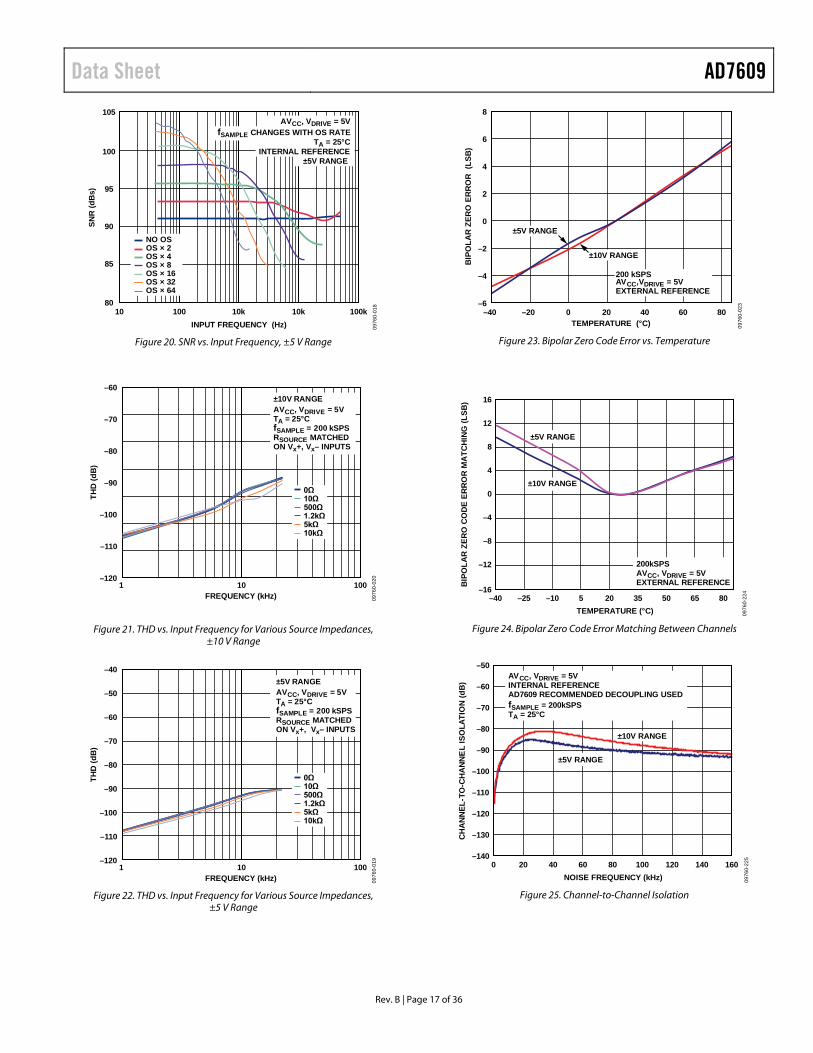
Table 6. Pin Function Descriptions Pin No. Type1 Mnemonic Description 1, 37, 38, 48 P AVCC Analog Supply Voltage 4.75 V to 5.25 V. This supply voltage is applied to the internal front-end
amplifiers and to the ADC core. These supply pins should be decoupled to AGND. 2, 26, 35, 40, 41, 47
P AGND Analog Ground. This pin is the ground reference point for all analog circuitry on the AD7609. All analog input signals and external reference signals should be referred to these pins. All six of these AGND pins should connect to the AGND plane of a system.
23 P VDRIVE Logic Power Supply Input. The voltage (2.3 V to 5 V) supplied at this pin determines the operating voltage of the interface. This pin is nominally at the same supply as the supply of the host interface (that is, DSP, FPGA).
36, 39 P REGCAP Decoupling Capacitor Pins for Voltage Output from Internal Regulator. These output pins should be decoupled separately to AGND using a 1 μF capacitor. The voltage on these output pins is in the range of 2.5 V to 2.7 V.
49, 51, 53, 55, 57, 59, 61, 63
AI+ V1+ to V8+ Analog Input V1+ to Analog Input V8+. These pins are the positive terminal of the true differential analog inputs. The analog input range of these channels is determined by the RANGE pin.
50, 52, 54, 56, 58, 60, 62, 64
AI− V1− to V8− Analog Input V1− to Analog Input V8−. These are the negative terminals of the true differential analog inputs. The analog input range of these channels is determined by the RANGE pin. The signal on this pin should be 180° out of phase with the corresponding Vx+ pin.
42 REF REFIN/ REFOUT
Reference Input/ Reference Output. The on-chip reference of 2.5 V is available on this pin for external use if the REF SELECT pin is set to a logic high. Alternatively, the internal reference can be disabled by setting the REF SELECT pin to a logic low and an external reference of 2.5 V can be applied to this input. See the Internal/External Reference section. Decoupling is required on this pin for both the internal or external reference options. A 10 µF capacitor should be applied from this pin to ground close to the REFGND pins.
34 DI REF SELECT Internal/External Reference Selection Input. Logic input. If this pin is set to logic high, the internal reference is selected and is enabled. If this pin is set to logic low, the internal reference is disabled and an external reference voltage must be applied to the REFIN/REFOUT pin.
44, 45 REF REFCAPA, REFCAPB
Reference Buffer Output Force/Sense Pins. These pins must be connected together and decoupled to AGND using a low ESR 10 μF ceramic capacitor.
43, 46 REF REFGND Reference Ground Pins. These pins should be connected to AGND.
Rev. B | Page 12 of 36

Data Sheet AD7609
Pin No. Type1 Mnemonic Description 8 DI RANGE Analog Input Range Selection. Logic input. The polarity on this pin determines the input range of the
analog input channels. If this pin is tied to a logic high, the analog input range is ±10 V for all channels. If this pin is tied to a logic low, the analog input range is ±5 V for all channels. A logic change on this pin has an immediate effect on the analog input range. Changing this pin during a conversion is not recommended. See the Analog Input section for more details.
6 DI PAR/ SER SEL
Parallel/Serial Interface Selection Input. Logic input. If this pin is tied to a logic low, the parallel interface is selected. If this pin is tied to a logic high, the serial interface is selected. In serial mode, the RD/SCLK pin functions as the serial clock input. The DB7/DOUTA and DB8/DOUTB pins function as serial data outputs. When the serial interface is selected, the DB[15:9] and DB[6:0] pins should be tied to AGND.
9, 10 DI CONVST A, CONVST B
Conversion Start Input A, Conversion Start Input B. Logic inputs. These logic inputs are used to initiate conversions on the analog input channels. For simultaneous sampling of all input channels, CONVST A and CONVST B can be shorted together and a single conversion start signal applied. Alternatively, CONVST A can be used to initiate simultaneous sampling for V1, V2, V3, and V4, and CONVST B can be used to initiate simultaneous sampling on the other analog inputs (V5, V6, V7, and V8). This is only possible when oversampling is not switched on. When the CONVST A or CONVST B pin transitions from low to high, the front-end track-and-hold circuitry for their respective analog inputs is set to hold. This function allows a phase delay to be created inherently between the sets of analog inputs.
13 DI CS Chip Select. This active low logic input frames the data transfer. When both CS and RD are logic low in parallel mode, the output bus (DB[15:0]) is enabled and the conversion result is output on the parallel data bus lines. In serial mode, the CS is used to frame the serial read transfer and clocks out the MSB of the serial output data.
12 DI RD/SCLK Parallel Data Read Control Input When Parallel Interface is Selected (RD)/Serial Clock Input When Serial Interface is Selected (SCLK). When both CS and RD are logic low in parallel mode, the output bus is enabled. In parallel mode, two RD pulses are required to read the full 18 bits of conversion results from each channel. The first RD pulse outputs DB[17:2], and the second RD pulses outputs DB[1:0]. In serial mode, this pin acts as the serial clock input for data transfers. The CS falling edge takes the data output lines, DOUTA and DOUTB, out of three-state and clocks out the MSB of the conversion result. The rising edge of SCLK clocks all subsequent data bits onto the serial data outputs, DOUTA and DOUTB. For further information, see the Conversion Control section.
14 DO BUSY Busy Output. This pin transitions to a logic high after both CONVST A and CONVST B rising edges and indicates that the conversion process has started. The BUSY output remains high until the conversion process for all channels is complete. The falling edge of BUSY signals that the conversion data is being latched into the output data registers and will be available to be read after a time, t4. Any data read while BUSY is high should be complete before the falling edge of BUSY occurs. Rising edges on CONVST A or CONVST B have no effect while the BUSY signal is high.
11 DI RESET Reset Input. When set to logic high, the rising edge of RESET resets the AD7609. The part must receive a RESET pulse after power-up. To achieve the specified performance after the RESET signal, the tWAKE_UP
SHUTDOWN time should elapse between power-on and the RESET pulse. The RESET high pulse should be typically 100 ns wide. If a RESET pulse is applied during a conversion, the conversion is aborted. If a RESET pulse is applied during a read, the contents of the output registers reset to all zeros.
15 DO FRSTDATA Digital Output. The FRSTDATA output signal indicates when the first channel, V1, is being read back on either the parallel or serial interface. When the CS input is high, the FRSTDATA output pin is in three-state. The falling edge of CS takes FRSTDATA out of three-state. In parallel mode, the falling edge of RD corresponding to the result of V1 then sets the FRSTDATA pin high, indicating that the result from V1 is available on the output data bus. The FRSTDATA output returns to a logic low following the third falling edge of RD. In serial mode, FRSTDATA goes high on the falling edge of CS as this clocks out the MSB of V1 on DOUTA. It returns low on the 18th SCLK falling edge after the CS falling edge. See the Conversion Control section for more details.
7 DI STBY Standby Mode Input. This pin is used to place the AD7609 into one of two power-down modes: standby mode or shutdown mode. The power-down mode entered depends on the state of the RANGE pin, as shown in Table 8. When in standby mode, all circuitry except the on-chip reference, regulators, and regulator buffers is powered down. When in shutdown mode, all circuitry is powered down.
Rev. B | Page 13 of 36
AD7609 Data Sheet
Pin No. Type1 Mnemonic Description 5, 4, 3 DI OS [2:0] Oversampling Mode Pins. Logic inputs. These inputs are used to select the oversampling ratio. OS 2 is
the MSB control bit, and OS 0 is the LSB control bit. See the Digital Filter section for additional details on the oversampling mode of operation and Table 9 for oversampling bit decoding.
33 DO/DI DB15 Parallel Output Data Bits, Data Bit 15. When PAR/SER SEL = 0, this pin acts as three-state parallel digital output pin. This pin is used to output DB17 of the conversion result during the first RD pulse and DB1 of the same conversion result during the second RD pulse. When PAR/SER SEL = 1, this pin should be tied to AGND.
32 DO/DI DB14 Parallel Output Data Bits, Data Bit 14. When PAR/SER SEL = 0, this pin acts as three-state parallel digital output pin. When CS and RD are low, this pin is used to output DB16 of the conversion result during the first RD pulse and DB0 of the same conversion result during the second RD pulse. When PAR/SER SEL = 1, this pin should be tied to AGND.
31 to 27 DO DB[13:9] Parallel Output Data Bits, Data Bit 13 to Data Bit 9. When PAR/SER SEL = 0, these pins act as three-state parallel digital input/output pins. When CS and RD are low, these pins are used to output DB15 to DB11 of the conversion result during the first RD pulse and output 0 during the second RD pulse. When PAR/SER SEL = 1, these pins should be tied to AGND.
24 DO DB7/DOUTA Parallel Output Data Bit 7 (DB7)/Serial Interface Data Output Pin (DOUTA). When PAR/SER SEL = 0, this pins acts as a three-state parallel digital input/output pin. When CS and RD are low, this pin is used to output DB9 of the conversion result. When PAR/SER SEL = 1, this pin functions as DOUTA and outputs serial conversion data. See the Conversion Control section for further details.
25 DO DB8/DOUTB Parallel Output Data Bit 8 (DB8)/Serial Interface Data Output Pin (DOUTB). When PAR/SER SEL = 0, this pins acts as a three-state parallel digital input/output pin. When CS and RD are low, this pin is used to output DB10 of the conversion result. When PAR/SER SEL = 1, this pin functions as DOUTB and outputs serial conversion data. See the Conversion Control section for further details.
22 to 16 DO DB[6:0] Parallel Output Data Bits, Data Bit 6 to Data Bit 0. When PAR/SER SEL = 0, these pins act as three-state parallel digital input/output pins. When CS and RD are low, these pins are used to output DB8 to DB2 of the conversion result during the first RD pulse and output 0 during the second RD pulse. When PAR/SER SEL = 1, these pins should be tied to AGND.
1 Refers to classification of pin type; P denotes power, AI denotes analog input, REF denotes reference, DI denotes digital input, DO denotes digital output.
Rev. B | Page 14 of 36
Data Sheet AD7609
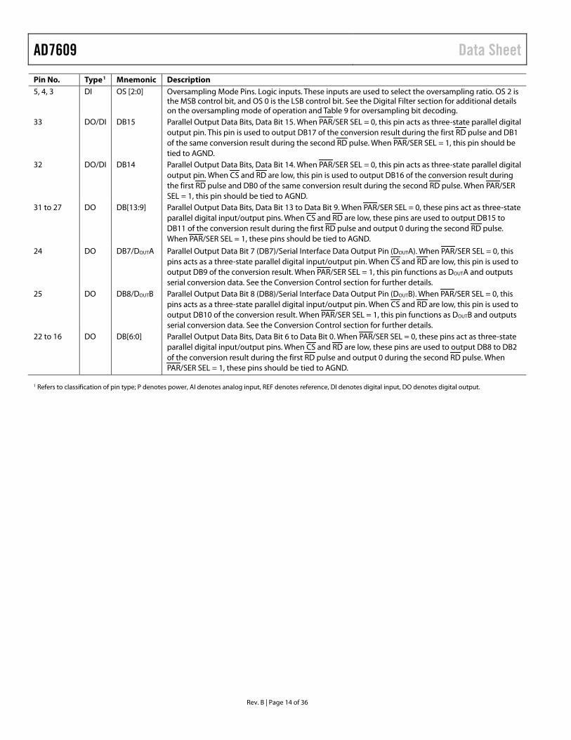
TYPICAL PERFORMANCE CHARACTERISTICS
–160
–140
–120
–100
–80
–60
–40
–20
0
0 20k 40k 60k 80k 100k
SNR
(dB
)
INPUT FREQUENCY (Hz)
AVCC, VDRIVE = 5VINTERNAL REFERENCE±10V RANGEfSAMPLE = 200 kSPSfIN = 1kHz16384 POINT FFTSNR = 91.52dBTHD = –111.05dB
0976
0-00
8
Figure 8. FFT Plot, ±10 V Range
–160
–140
–120
–100
–80
–60
–40
–20
0
0 20k 40k 60k 80k 100k
AM
PLIT
UD
E (d
B)
INPUT FREQUENCY (Hz)
AVCC, VDRIVE = 5VINTERNAL REFERENCE±5V RANGEfSAMPLE = 200kSPSf IN = 1kHz16,384 POINT FFTSNR = 91.12dBTHD = –109.77dB
0976
0-00
9
Figure 9. FFT Plot, ±5 V Range
–160
–140
–120
–100
–80
–60
–40
–20
0
0 1 2 3 4 5 6
AM
PLIT
UD
E (d
B)
INPUT FREQUENCY (kHz) 0976
0-10
9
AVCC, VDRIVE = 5VINTERNAL REFERENCE±10V RANGEfSAMPLE = 12.5kSPSfIN = 1Hz8192 POINT FFTSNR = 100.71dBTHD: –111.74dB
Figure 10. FFT Plot, ±10 V Range
–3
–2
–1
0
1
2
3
0
32,7
68
INL
(LSB
)
CODE
65,5
36
98,3
04
131,
072
163,
840
196,
608
229,
376
±10V RANGEAVCC, VDRIVE = 5VTA = 25°CfSAMPLE = 200 kSPSWCP INL = 1.69 LSBWCN INL = –1.3 LSB
0976
0-01
0
Figure 11. Typical INL, ±10 V Range
0
32,7
68
CODE
65,5
36
98,3
04
131,
072
163,
840
196,
608
229,
376
0976
0-01
1
–1.0
0
1.0
0.8
0.6
0.4
0.2
–0.2
–0.4
–0.6
–0.8
DN
L (L
SB)
±10V RANGEAVCC, VDRIVE = 5VTA = 25°CfSAMPLE = 200 kSPSWCP DNL = 0.33 LSBWCN DNL = –0.32 LSB
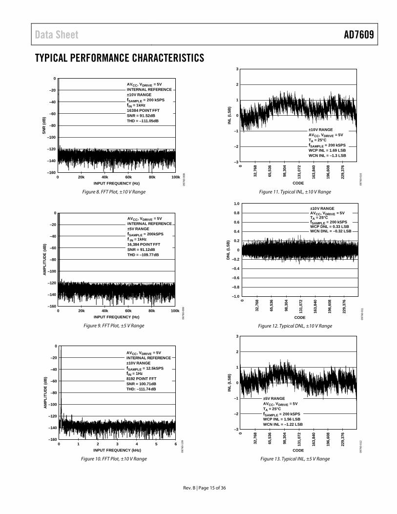
Figure 12. Typical DNL, ±10 V Range
–3
–2
–1
0
1
2
3
0
32,7
68
INL
(LSB
)
CODE
65,5
36
98,3
04
131,
072
163,
840
196,
608
229,
376
±5V RANGEAVCC, VDRIVE = 5VTA = 25°CfSAMPLE = 200 kSPSWCP INL = 1.56 LSBWCN INL = –1.22 LSB
0976
0-01
2
Figure 13. Typical INL, ±5 V Range
Rev. B | Page 15 of 36
AD7609 Data Sheet
0
32,7
68
CODE
65,5
36
98,3
04
131,
072
163,
840
196,
608
229,
376
0976
0-01
3
DN
L (L
SB)
–1.0
0
1.0
0.8
0.6
0.4
0.2
–0.2
–0.4
–0.6
–0.8
±5V RANGEAVCC, VDRIVE = 5VTA = 25°CfSAMPLE = 200 kSPSWCP INL = 0.45 LSBWCN INL = –0.38 LSB
Figure 14. Typical DNL, ±5 V Range
80
60
40
20
0
–20
–40
–60
–40 –25 –10 5 20 35 50 65 80–80
NFS
ER
RO
R (L
SB)
TEMPERATURE (°C)
200kSPSAVCC, VDRIVE = 5VEXTERNAL REFERENCE
±5V RANGE
±10V RANGE
0976
0-11
7
Figure 15. NFS Error vs. Temperature
80
60
40
20
0
–20
–40
–60
–40 –25 –10 5 20 35 50 65 80–80
PFS
ERR
OR
(LSB
)
TEMPERATURE (°C)
200kSPSAVCC, VDRIVE = 5VEXTERNAL REFERENCE
±5V RANGE
±10V RANGE
0976
0-11
8
Figure 16. PFS Error vs. Temperature
40
–40 –25 –10 5 20 35 50 65 80–40
–32
–24
–16
–8
0
8
16
24
32
NFS
/PFS
CH
AN
NEL
MA
TCH
ING
(LSB
)
TEMPERATURE (°C)
±10V RANGEAVCC, VDRIVE = 5VEXTERNAL REFERENCE
PFS ERROR
NFS ERROR
0976
0-21
8
Figure 17. NFS and PFS Error Matching
10
8
6
4
2
0
0 120k100k80k60k40k20k–2
PFS/
NFS
ER
RO
R (%
FS)
SOURCE RESISTANCE (Ω)
AVCC, VDRIVE = 5VfSAMPLE = 200 kSPSTA = 25°CEXTERNAL REFERENCESOURCE RESISTANCE IS MATCHED ONTHE V– INPUT±10V AND ±5V RANGE
0976
0-21
9
Figure 18. PFS and NFS Error vs. Source Resistance
80
85
90
95
100
105
10 100 10k 10k 100k
SNR
(dB
s)
INPUT FREQUENCY (Hz)
NO OSOS × 2OS × 4OS × 8OS × 16OS × 32OS × 64
AVCC, VDRIVE = 5VfSAMPLE CHANGES WITH OS RATE
TA = 25°CINTERNAL REFERENCE
±10V RANGE09
760-
017
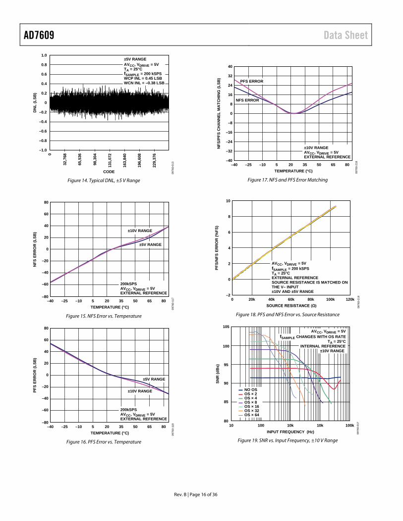
Figure 19. SNR vs. Input Frequency, ±10 V Range
Rev. B | Page 16 of 36
Data Sheet AD7609
80
85
90
95
100
105
10 100 10k 10k 100k
SNR
(dB
s)
INPUT FREQUENCY (Hz)
NO OSOS × 2OS × 4OS × 8OS × 16OS × 32OS × 64
AVCC, VDRIVE = 5VfSAMPLE CHANGES WITH OS RATE
TA = 25°CINTERNAL REFERENCE
±5V RANGE
0976
0-01
8
Figure 20. SNR vs. Input Frequency, ±5 V Range
–120
–110
–100
–90
–80
–70
–60
1 10 100
THD
(dB
)
FREQUENCY (kHz)
±10V RANGEAVCC, VDRIVE = 5VTA = 25°CfSAMPLE = 200 kSPSRSOURCE MATCHEDON Vx+, Vx– INPUTS
10kΩ5kΩ
10Ω0Ω
1.2kΩ500Ω
0976
0-02
0
Figure 21. THD vs. Input Frequency for Various Source Impedances, ±10 V Range
–120
–110
–100
–90
–80
–70
–60
–50
–40
1 10 100
THD
(dB
)
FREQUENCY (kHz) 0976
0-01
9
±5V RANGEAVCC, VDRIVE = 5VTA = 25°CfSAMPLE = 200 kSPSRSOURCE MATCHEDON Vx+, Vx– INPUTS
10kΩ5kΩ
10Ω0Ω
1.2kΩ500Ω
Figure 22. THD vs. Input Frequency for Various Source Impedances,
±5 V Range
200 kSPSAVCC,VDRIVE = 5VEXTERNAL REFERENCE
0976
0-02
3
±5V RANGE
±10V RANGE
–6
–4
–2
0
2
4
6
8
–40 –20 0 20 40 60 80
BIP
OLA
R Z
ERO
ER
RO
R (
LSB
)
TEMPERATURE (°C) Figure 23. Bipolar Zero Code Error vs. Temperature
16
12
8
4
0
–4
–8
–12
–40 –25 –10 5 20 35 50 65 80–16B
IPO
LAR
ZER
O C
OD
E ER
RO
R M
ATC
HIN
G (L
SB)
TEMPERATURE (°C)
200kSPSAVCC, VDRIVE = 5VEXTERNAL REFERENCE
±5V RANGE
±10V RANGE
0976
0-22
4
Figure 24. Bipolar Zero Code Error Matching Between Channels
–50
–60
–70
–80
–90
–100
–110
–120
–130
0 16014012010080604020–140
CH
AN
NEL
-TO
-CH
AN
NE
L IS
OL A
TIO
N (d
B)
NOISE FREQUENCY (kHz)
AVCC, VDRIVE = 5VINTERNAL REFERENCEAD7609 RECOMMENDED DECOUPLING USEDfSAMPLE = 200kSPSTA = 25°C
0976
0-22
5
±5V RANGE
±10V RANGE
Figure 25. Channel-to-Channel Isolation
Rev. B | Page 17 of 36
AD7609 Data Sheet
0976
0-02
380
85
90
95
100
105
110
NO OS OS × 2 OS × 4 OS × 8 OS × 16 OS × 32 OS × 64
DYN
AM
IC R
AN
GE
(dB
)
OVERSAMPLING RATIO
AVCC = VDRIVE = 5VTA = 25°CINTERNAL REFERENCEfSAMPLE SCALES WITH OS RATIO
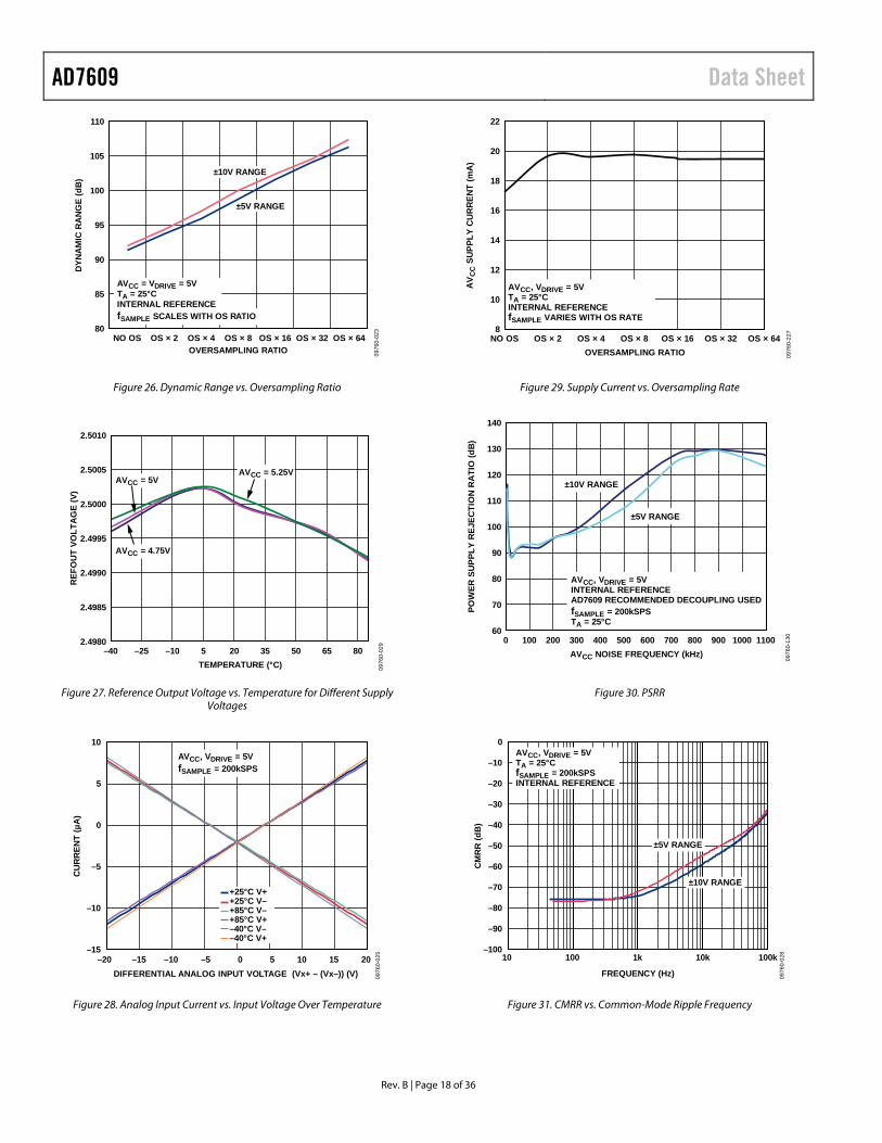
±10V RANGE
±5V RANGE
Figure 26. Dynamic Range vs. Oversampling Ratio
2.5010
2.5005
2.5000
2.4995
2.4990
2.4985
–40 –25 –10 5 20 35 50 65 802.4980
REF
OU
T VO
LTA
GE
(V)
TEMPERATURE (°C)
AVCC = 4.75V
AVCC = 5VAVCC = 5.25V
0976
0-02
9
Figure 27. Reference Output Voltage vs. Temperature for Different Supply Voltages
–15
–10
–5
0
5
10
–20 –15 –10 –5 0 5 10 15 20
CU
RR
ENT
(µA
)
DIFFERENTIAL ANALOG INPUT VOLTAGE (Vx+ – (Vx–)) (V)
+25°C V++25°C V–+85°C V–+85°C V+–40°C V––40°C V+
AVCC, VDRIVE = 5VfSAMPLE = 200kSPS
0976
0-02
5
Figure 28. Analog Input Current vs. Input Voltage Over Temperature
22
20
18
16
14
12
10
8
AV C
C S
UPP
LY C
UR
REN
T (m
A)
OVERSAMPLING RATIO
AVCC, VDRIVE = 5VTA = 25°CINTERNAL REFERENCEfSAMPLE VARIES WITH OS RATE
NO OS OS × 2 OS × 4 OS × 8 OS × 16 OS × 32 OS × 64
0976
0-22
7
Figure 29. Supply Current vs. Oversampling Rate
140
0 1100100090080070060050040030020010060
70
80
90
100
110
120
130
POW
ER S
UPP
LY R
EJEC
TIO
N R
ATI
O (d
B)
AVCC NOISE FREQUENCY (kHz)
AVCC, VDRIVE = 5VINTERNAL REFERENCEAD7609 RECOMMENDED DECOUPLING USEDfSAMPLE = 200kSPSTA = 25°C
±10V RANGE
±5V RANGE
0976
0-13
0
Figure 30. PSRR
–100
–90
–80
–70
–60
–50
–40
–30
–20
0
–10
10 100 1k 10k 100k
CM
RR
(dB
)
FREQUENCY (Hz)
±10V RANGE
±5V RANGE
AVCC, VDRIVE = 5VTA = 25°CfSAMPLE = 200kSPSINTERNAL REFERENCE
0976
0-02
8
Figure 31. CMRR vs. Common-Mode Ripple Frequency
Rev. B | Page 18 of 36
Data Sheet AD7609
TERMINOLOGY Integral Nonlinearity The maximum deviation from a straight line passing through the endpoints of the ADC transfer function. The endpoints of the transfer function are zero scale, a ½ LSB below the first code transition, and full scale at ½ LSB above the last code transition.
Differential Nonlinearity The difference between the measured and the ideal 1 LSB change between any two adjacent codes in the ADC.
Bipolar Zero Code Error The deviation of the midscale transition (all 1s to all 0s) from the ideal VIN voltage, that is, AGND.
Bipolar Zero Code Error Match The difference in bipolar zero code error between any two input channels.
Positive Full-Scale Error The last transition (from 011 . . . 10 to 011 . . . 11 in twos complement coding) should occur for an analog voltage 1½ LSB below the nominal full scale (9.99977 V for the ±10 V range and 4.99988 V for the ±5 V range). The positive full-scale error is the deviation of the actual level of the last transition from the ideal level.
Positive Full-Scale Error Match The difference in positive full-scale error between any two input channels.
Negative Full-Scale Error The first transition (from 100 . . . 00 to 100 . . . 01 in twos complement coding) should occur for an analog voltage ½ LSB above the negative full scale (−9.999923 V for the ±10 V range and −4.9999618 for the ±5 V range). The negative full-scale error is the deviation of the actual level of the first transition from the ideal level.
Negative Full-Scale Error Match The difference in negative full-scale error between any two input channels.
Track-and-Hold Acquisition Time The track-and-hold amplifier returns to track mode at the end of the conversion. The track-and-hold acquisition time is the time required for the output of the track-and-hold amplifier to reach its final value, within ±1 LSB, after the end of the conversion. See the Track-and-Hold Amplifiers section for more details.
Signal-to-(Noise + Distortion) Ratio The measured ratio of signal-to-(noise + distortion) at the output of the ADC. The signal is the rms amplitude of the fundamental. Noise is the sum of all nonfundamental signals up to half the sampling frequency (fS/2, excluding dc). The ratio depends on the number of quantization levels in the digitization process: the more levels, the smaller the quantization noise. The theoretical signal-to-(noise + distortion) ratio for an ideal N-bit converter with a sine wave input is given by
Signal-to-(Noise + Distortion) = (6.02 N + 1.76) dB
Thus, for an 18-bit converter, this is 110.12 dB.
Total Harmonic Distortion (THD) The ratio of the rms sum of the harmonics to the fundamental. For the AD7609, it is defined as
THD (dB) =
20log1
98765432
VVVVVVVVV 22222222 +++++++
where: V1 is the rms amplitude of the fundamental. V2 to V9 are the rms amplitudes of the second through ninth harmonics.
Peak Harmonic or Spurious Noise The ratio of the rms value of the next largest component in the ADC output spectrum (up to fS/2, excluding dc) to the rms value of the fundamental. Normally, the value of this specification is determined by the largest harmonic in the spectrum, but for ADCs where the harmonics are buried in the noise floor, it is determined by a noise peak.
Intermodulation Distortion With inputs consisting of sine waves at two frequencies, fa and fb, any active device with nonlinearities creates distortion products at sum and difference frequencies of mfa ± nfb, where m, n = 0, 1, 2, 3. Intermodulation distortion terms are those for which neither m nor n is equal to 0. For example, the second-order terms include (fa + fb) and (fa − fb), and the third-order terms include (2fa + fb), (2fa − fb), (fa + 2fb), and (fa − 2fb).
The calculation of the intermodulation distortion is per the THD specification, where it is the ratio of the rms sum of the individual distortion products to the rms amplitude of the sum of the fundamentals expressed in decibels (dB).
Rev. B | Page 19 of 36

AD7609 Data Sheet Power Supply Rejection (PSR) Variations in power supply affect the full-scale transition but not the converter’s linearity. Power supply rejection is the maximum change in full-scale transition point due to a change in power supply voltage from the nominal value. The power supply rejection ratio is defined as the ratio of the power in the ADC output at full-scale frequency, f, to the power of a 200 mV p-p sine wave applied to the ADC VDD and VSS supplies of Frequency fS.
PSRR (dB) = 10 log (Pf/PfS)
where: Pf is equal to the power at Frequency f in the ADC output. PfS is equal to the power at Frequency fS coupled onto the VDD and VSS supplies.
Channel-to-Channel Isolation Channel-to-channel isolation is a measure of the level of crosstalk between any two channels. It is measured by applying a full-scale, 10 kHz sine wave signal to all unselected input channels and determining the degree to which the signal attenuates in the selected channel with a 1 kHz signal.
Common-Mode Rejection Ratio (CMRR) CMRR is defined as the ratio of the power in the ADC common-mode input at full-scale frequency, f, to the power in the output of a full-scale p-p sine wave applied to the common-mode voltage of VINX+ and VINX− of frequency, fS,
CMRR (dB) = 20 log (Pf/PfS)
where: Pf is equal to the power at Frequency f in the ADC input. PfS is equal to the power at Frequency fS in the ADC output.
Rev. B | Page 20 of 36
Data Sheet AD7609
Rev. B | Page 21 of 36
THEORY OF OPERATION CONVERTER DETAILS The AD7609 is a data acquisition system that employs a high speed, low power, charge redistribution successive approxima-tion analog-to-digital converter (ADC) and allows the simultaneous sampling of eight true differential analog input channels. The analog inputs on the AD7609 can accept true bipolar input signals. The RANGE pin is used to select either ±10 V or ±5 V as the input range. The AD7609 operates from a single 5 V supply.
The AD7609 contains input clamp protection, input signal scaling amplifiers, a second-order antialiasing filter, track-and-hold amplifiers, an on-chip reference, reference buffers, a high speed ADC, a digital filter, and high speed parallel and serial interfaces. Sampling on the AD7609 is controlled using CONVST x signals.
ANALOG INPUT Analog Input Ranges
The AD7609 can handle true bipolar input voltages. The logic level on the RANGE pin determines the analog input range of all analog input channels. If this pin is tied to a logic high, the analog input range is ±10 V for all channels. If this pin is tied to a logic low, the analog input range is ±5 V for all channels. A logic change on this pin has an immediate effect on the analog input range; however, there is a settling time of 80 μs typically, in addition to the normal acquisition time requirement. The recommended practice is to hardwire the RANGE pin according to the desired input range for the system signals.
During normal operation, the applied analog input voltage should remain within the analog input range selected via the RANGE pin. A RESET pulse must be applied to the part to ensure the analog input channels are configured for the range selected.
When in a power-down mode, it is recommended to tie the analog inputs together or both analog input pins (Vx+, Vx−) to GND. As per the Analog Input Clamp Protection section, the overvoltage clamp protection is recommended for use in transient overvoltage conditions, and should not remain active for extended periods. Stressing the analog inputs outside of these conditions may degrade the Bipolar Zero Code error and THD performance of the AD7609.
Analog Input Impedance
The analog input impedance of the AD7609 is 1 MΩ. This is a fixed input impedance and does not vary with the AD7609 sam-pling frequency. This high analog input impedance eliminates the need for a driver amplifier in front of the AD7609 allowing for direct connection to the source or sensor. With the need for a driver amplifier eliminated, bipolar supplies can be removed from the signal chain, which are often a source of noise in a system.
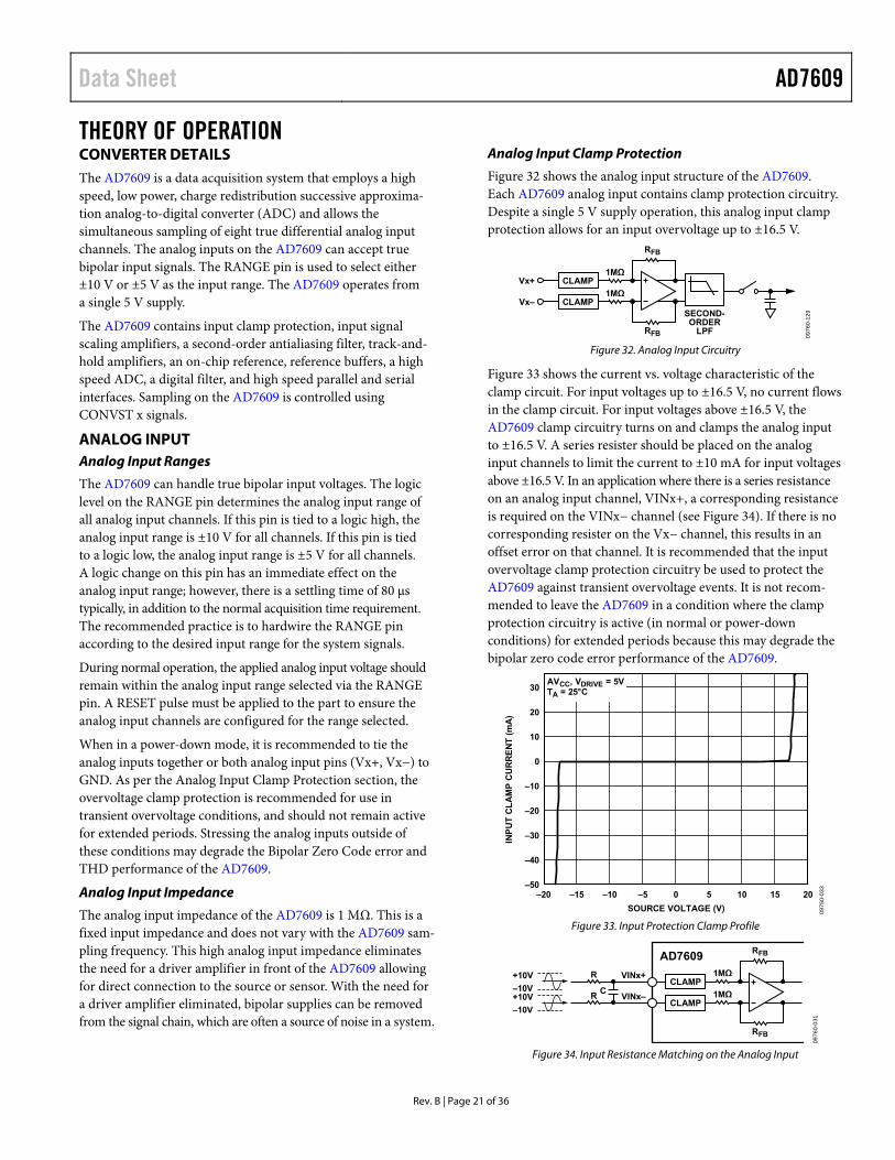
Analog Input Clamp Protection
Figure 32 shows the analog input structure of the AD7609. Each AD7609 analog input contains clamp protection circuitry. Despite a single 5 V supply operation, this analog input clamp protection allows for an input overvoltage up to ±16.5 V.
1MΩCLAMPVx+
1MΩCLAMPVx–
SECOND-ORDER
LPF
RFB
RFB 0976
0-12
9
Figure 32. Analog Input Circuitry
Figure 33 shows the current vs. voltage characteristic of the clamp circuit. For input voltages up to ±16.5 V, no current flows in the clamp circuit. For input voltages above ±16.5 V, the AD7609 clamp circuitry turns on and clamps the analog input to ±16.5 V. A series resister should be placed on the analog input channels to limit the current to ±10 mA for input voltages above ±16.5 V. In an application where there is a series resistance on an analog input channel, VINx+, a corresponding resistance is required on the VINx− channel (see Figure 34). If there is no corresponding resister on the Vx− channel, this results in an offset error on that channel. It is recommended that the input overvoltage clamp protection circuitry be used to protect the AD7609 against transient overvoltage events. It is not recom-mended to leave the AD7609 in a condition where the clamp protection circuitry is active (in normal or power-down conditions) for extended periods because this may degrade the bipolar zero code error performance of the AD7609.
0976
0-03
3
30
–50
–40
–30
–20
–10
0
10
20
–20 –15 –10 –5 0 5 10 15 20
INP
UT
CL
AM
P C
UR
RE
NT
(m
A)
SOURCE VOLTAGE (V)
AVCC, VDRIVE = 5VTA = 25°C
Figure 33. Input Protection Clamp Profile
1MΩCLAMP
VINx+
1MΩCLAMP
VINx–
RFB
RFB
C
R
R+10V
–10V
AD7609
0976
0-03
1
+10V
–10V
Figure 34. Input Resistance Matching on the Analog Input
AD7609 Data Sheet Analog Input Antialiasing Filter
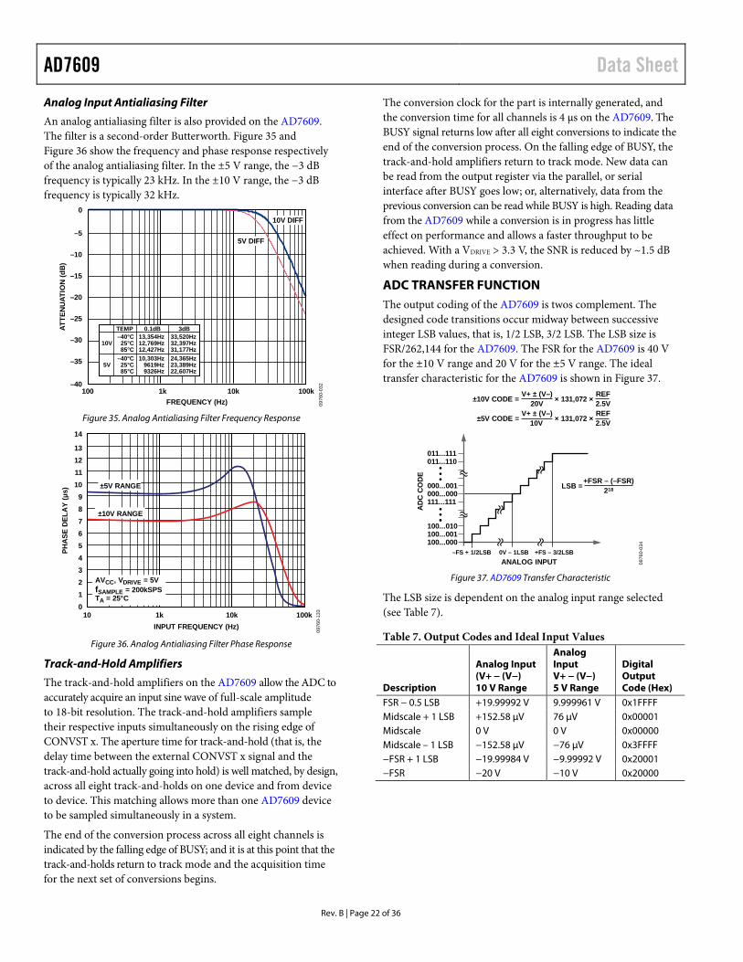
An analog antialiasing filter is also provided on the AD7609. The filter is a second-order Butterworth. Figure 35 and Figure 36 show the frequency and phase response respectively of the analog antialiasing filter. In the ±5 V range, the −3 dB frequency is typically 23 kHz. In the ±10 V range, the −3 dB frequency is typically 32 kHz.
–40
–35
–30
–25
–20
–15
–10
–5
0
100 1k 10k 100k
ATTE
NU
ATIO
N (d
B)
FREQUENCY (Hz)
10V DIFF
5V DIFF
0976
0-03
2
10V
0.1dBTEMP 3dB–40°C 13,354Hz 33,520Hz
25°C 12,769Hz 32,397Hz85°C 12,427Hz 31,177Hz
5V–40°C 10,303Hz 24,365Hz
25°C 9619Hz 23,389Hz85°C 9326Hz 22,607Hz
Figure 35. Analog Antialiasing Filter Frequency Response
0976
0-13
3
10 100k10k1k
PHA
SE D
ELA
Y (µ
s)
INPUT FREQUENCY (Hz)
0123456789
10111213
14
±5V RANGE
±10V RANGE
AVCC, VDRIVE = 5VfSAMPLE = 200kSPSTA = 25°C
Figure 36. Analog Antialiasing Filter Phase Response
Track-and-Hold Amplifiers
The track-and-hold amplifiers on the AD7609 allow the ADC to accurately acquire an input sine wave of full-scale amplitude to 18-bit resolution. The track-and-hold amplifiers sample their respective inputs simultaneously on the rising edge of CONVST x. The aperture time for track-and-hold (that is, the delay time between the external CONVST x signal and the track-and-hold actually going into hold) is well matched, by design, across all eight track-and-holds on one device and from device to device. This matching allows more than one AD7609 device to be sampled simultaneously in a system.
The end of the conversion process across all eight channels is indicated by the falling edge of BUSY; and it is at this point that the track-and-holds return to track mode and the acquisition time for the next set of conversions begins.
The conversion clock for the part is internally generated, and the conversion time for all channels is 4 µs on the AD7609. The BUSY signal returns low after all eight conversions to indicate the end of the conversion process. On the falling edge of BUSY, the track-and-hold amplifiers return to track mode. New data can be read from the output register via the parallel, or serial interface after BUSY goes low; or, alternatively, data from the previous conversion can be read while BUSY is high. Reading data from the AD7609 while a conversion is in progress has little effect on performance and allows a faster throughput to be achieved. With a VDRIVE > 3.3 V, the SNR is reduced by ~1.5 dB when reading during a conversion.
ADC TRANSFER FUNCTION The output coding of the AD7609 is twos complement. The designed code transitions occur midway between successive integer LSB values, that is, 1/2 LSB, 3/2 LSB. The LSB size is FSR/262,144 for the AD7609. The FSR for the AD7609 is 40 V for the ±10 V range and 20 V for the ±5 V range. The ideal transfer characteristic for the AD7609 is shown in Figure 37.
011...111011...110
000...001000...000111...111
100...010100...001100...000
–FS + 1/2LSB 0V – 1LSB +FS – 3/2LSB
AD
C C
OD
E
ANALOG INPUT
+FSR – (–FSR)218LSB =
V+ ± (V–)10V
REF2.5V±5V CODE = × 131,072 ×
V+ ± (V–)20V
REF2.5V±10V CODE = × 131,072 ×
0976
0-03
4
Figure 37. AD7609 Transfer Characteristic
The LSB size is dependent on the analog input range selected (see Table 7).
Table 7. Output Codes and Ideal Input Values
Description
Analog Input (V+ − (V−) 10 V Range
Analog Input V+ − (V−) 5 V Range
Digital Output Code (Hex)
FSR − 0.5 LSB +19.99992 V 9.999961 V 0x1FFFF Midscale + 1 LSB +152.58 µV 76 µV 0x00001 Midscale 0 V 0 V 0x00000 Midscale – 1 LSB −152.58 µV −76 µV 0x3FFFF −FSR + 1 LSB −19.99984 V −9.99992 V 0x20001 −FSR −20 V −10 V 0x20000
Rev. B | Page 22 of 36
Data Sheet AD7609
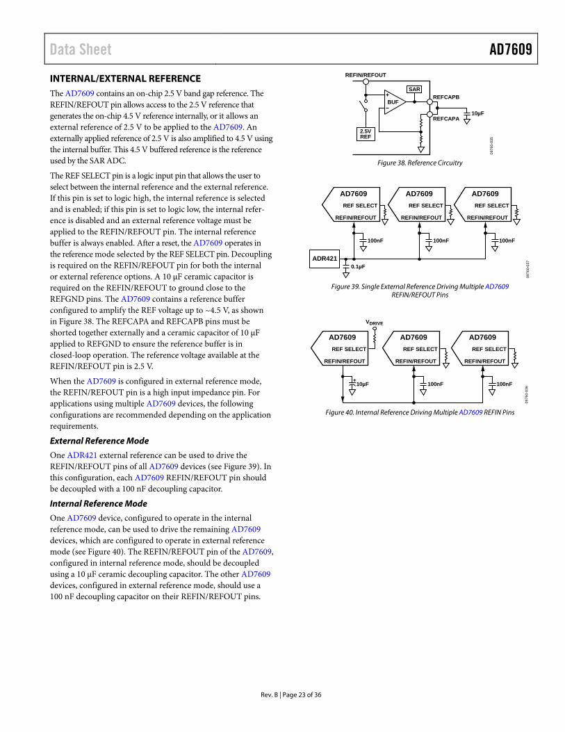
INTERNAL/EXTERNAL REFERENCE The AD7609 contains an on-chip 2.5 V band gap reference. The REFIN/REFOUT pin allows access to the 2.5 V reference that generates the on-chip 4.5 V reference internally, or it allows an external reference of 2.5 V to be applied to the AD7609. An externally applied reference of 2.5 V is also amplified to 4.5 V using the internal buffer. This 4.5 V buffered reference is the reference used by the SAR ADC.
The REF SELECT pin is a logic input pin that allows the user to select between the internal reference and the external reference. If this pin is set to logic high, the internal reference is selected and is enabled; if this pin is set to logic low, the internal refer-ence is disabled and an external reference voltage must be applied to the REFIN/REFOUT pin. The internal reference buffer is always enabled. After a reset, the AD7609 operates in the reference mode selected by the REF SELECT pin. Decoupling is required on the REFIN/REFOUT pin for both the internal or external reference options. A 10 µF ceramic capacitor is required on the REFIN/REFOUT to ground close to the REFGND pins. The AD7609 contains a reference buffer configured to amplify the REF voltage up to ~4.5 V, as shown in Figure 38. The REFCAPA and REFCAPB pins must be shorted together externally and a ceramic capacitor of 10 μF applied to REFGND to ensure the reference buffer is in closed-loop operation. The reference voltage available at the REFIN/REFOUT pin is 2.5 V.
When the AD7609 is configured in external reference mode, the REFIN/REFOUT pin is a high input impedance pin. For applications using multiple AD7609 devices, the following configurations are recommended depending on the application requirements.
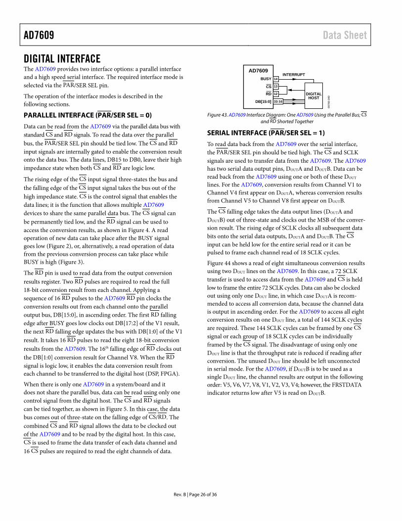
External Reference Mode
One ADR421 external reference can be used to drive the REFIN/REFOUT pins of all AD7609 devices (see Figure 39). In this configuration, each AD7609 REFIN/REFOUT pin should be decoupled with a 100 nF decoupling capacitor.
Internal Reference Mode
One AD7609 device, configured to operate in the internal reference mode, can be used to drive the remaining AD7609 devices, which are configured to operate in external reference mode (see Figure 40). The REFIN/REFOUT pin of the AD7609, configured in internal reference mode, should be decoupled using a 10 µF ceramic decoupling capacitor. The other AD7609 devices, configured in external reference mode, should use a 100 nF decoupling capacitor on their REFIN/REFOUT pins.
BUF
SAR
2.5VREF
REFCAPB
REFIN/REFOUT
REFCAPA10µF
0976
0-03
5
Figure 38. Reference Circuitry
AD7609REF SELECT
REFIN/REFOUT
AD7609REF SELECT
REFIN/REFOUT
100nF
0.1µF
100nF
AD7609REF SELECT
REFIN/REFOUT
100nF
ADR421
0976
0-03
7
Figure 39. Single External Reference Driving Multiple AD7609
REFIN/REFOUT Pins
AD7609REF SELECT
REFIN/REFOUT
+10µF
AD7609REF SELECT
REFIN/REFOUT
100nF
AD7609REF SELECT
REFIN/REFOUT
100nF
VDRIVE
0976
0-03
6
Figure 40. Internal Reference Driving Multiple AD7609 REFIN Pins
Rev. B | Page 23 of 36

AD7609 Data Sheet
TYPICAL CONNECTION DIAGRAM Figure 41 shows the typical connection diagram for the AD7609. There are four AVCC supply pins on the part that can be tied together and decoupled using a 100 nF capacitor at each supply pin and a 10 µF capacitor at the supply source. The AD7609 can operate with the internal reference or an externally applied reference. In this configuration, the AD7609 is config-ured to operate with the internal reference. When using a single AD7609 device on the board, the REFIN/REFOUT pin should be decoupled with a 10 µF capacitor. In an application with multiple AD7609 devices, see the Internal/External Reference section. The REFCAPA and REFCAPB pins are shorted together and decoupled with a 10 µF ceramic capacitor.
The VDRIVE supply is connected to the same supply as the pro-cessor. The voltage on VDRIVE controls the voltage value of the output logic signals. For layout, decoupling, and grounding hints, see the Layout Guidelines section.
After supplies are applied to the AD7609, a reset should be applied to the AD7609 to ensure that it is configured for the correct mode of operation.
POWER-DOWN MODES There are two power-down modes available on the AD7609. The STBY pin controls whether the AD7609 is in normal mode or one of the two power-down modes. The two power-down modes available are standby mode and shutdown mode. The power-down mode is selected through the state of the RANGE pin when the STBY pin is low. Table 8 shows the configurations required to choose the desired power-down mode. When the AD7609 is placed in standby mode, the current consumption is 8 mA maximum and power-up time is approximately 100 µs because the capacitor on the REFCAPA/REFCAPB pins must charge up. In standby mode, the on-chip reference and regulators remain powered up and the amplifiers and ADC core are powered down. When the AD7609 is placed in shutdown mode, the current consumption is 11 µA maximum and power up time is about 13 ms. In shutdown mode, all circuitry is powered down. When the AD7609 is powered up from shutdown mode, a reset signal must be applied to the AD7609 after the required power-up time has elapsed.
Table 8. Power-Down Mode Selection Power-Down Mode STBY RANGE Standby 0 1 Shutdown 0 0
AVCC
AGND
VDRIVE
+
REFIN/REFOUT
DB0 TO DB15
CONVST A, BCSRD
BUSYRESET
AD7609
1µF10µF100nF
DIGITAL SUPPLYVOLTAGE +2.3V TO +5V
ANALOG SUPPLYVOLTAGE 5V1
EIGHT DIFFERENTIALANALOG INPUT PAIRS
PARALLELINTERFACE
1DECOUPLING SHOWN ON THE AVCC PIN APPLIES TO EACH AVCC PIN (PIN 1, PIN 37, PIN 38, PIN 48).DECOUPLING CAPACITOR CAN BE SHARED BETWEEN AVCC PIN 37 AND PIN 38.
2DECOUPLING SHOWN ON THE REGCAP PIN APPLIES TO EACH REGCAP PIN (PIN 36, PIN 39).
REGCAP2
+10µF
REFCAPA
REFCAPB
OS 2OS 1OS 0
OVERSAMPLING
100nF
V1+
PAR/SER SEL
STBY
REF SELECT
RANGE
V2+
V3+
V4+
V5+
V6+
V7+
V8+
REFGND
V1–
V2–
V3–
V4–
V5–
V6–
V7–
V8–
VDRIVE
VDRIVE
MIC
RO
PRO
CES
SOR
/M
ICR
OC
ON
VER
TER
/D
SP
0976
0-03
8
Figure 41. Typical Connection Diagram
Rev. B | Page 24 of 36

Data Sheet AD7609
CONVERSION CONTROL Simultaneous Sampling on All Analog Input Channels
The AD7609 allows simultaneous sampling of all analog input channels. All channels are sampled simultaneously when both CONVST x pins (CONVST A, CONVST B) are tied together. A single CONVST x signal is used to control both CONVST x inputs. The rising edge of this common CONVST x signal initiates simultaneous sampling on all analog input channels.
The AD7609 contains an on-chip oscillator that is used to perform the conversions. The conversion time for all ADC channels is tCONV. The BUSY signal indicates to the user when conversions are in progress, so that when the rising edge of CONVST x is applied, BUSY goes logic high and transitions low at the end of the entire conversion process. The falling edge of the BUSY signal is used to place all eight track-and-hold amplifiers back into track mode. The falling edge of BUSY also indicates that the new data can now be read from the parallel bus (DB[15:0]) or the serial data lines, DOUTA and DOUTB.
Simultaneously Sampling Two Sets of Channels
The AD7609 also allows the analog input channels to be sampled simultaneously in two sets. This can be used in power line protection and measurement systems to compensate for phase differences between PT and CT transformers. In a 50 Hz system, this allows for up to 9° of phase compensation, and in a 60 Hz system, it allows for up to 10° of phase compensation.
This is accomplished by pulsing the two CONVST x pins inde-pendently and is only possible if oversampling is not in use. CONVST A is used to initiate simultaneous sampling of the first set of channels (V1 to V4). CONVST B is used to initiate simultaneous sampling on the second set of analog input channels (V5 to V8), as illustrated in Figure 42. On the rising edge of CONVST A, the track-and-hold amplifiers for the first set of channels are placed into hold mode. On the rising edge of CONVST B, the track-and-hold amplifiers for the second set of channels are placed into hold mode. The conversion process begins after both rising edges of CONVST x have occurred; therefore, BUSY goes high on the rising edge of the later CONVST x signal. The falling edge of BUSY also indicates that the new data can now be read from the parallel bus or the serial data lines, DOUTA and DOUTB. There is no change to the data read process when using two separate CONVST x signals.
Connect all unused analog input channel to AGND. The results for any unused channels are still included in the data read because all channels are always converted.
0976
0-03
9
CONVST A
CONVST B
BUSY
CS, RD
DATA: DB[15:0]
FRSTDATA
t5
tCONV
V1 TO V4 TRACK-AND-HOLDENTER HOLD
V5 TO V8 TRACK-AND-HOLDENTER HOLD
AD7609 CONVERTSON ALL 8 CHANNELS
V1 V8V2
Figure 42. Simultaneous Sampling on Channel Sets Using Independent CONVST A/CONVST B Signals—Parallel Mode
Rev. B | Page 25 of 36
AD7609 Data Sheet
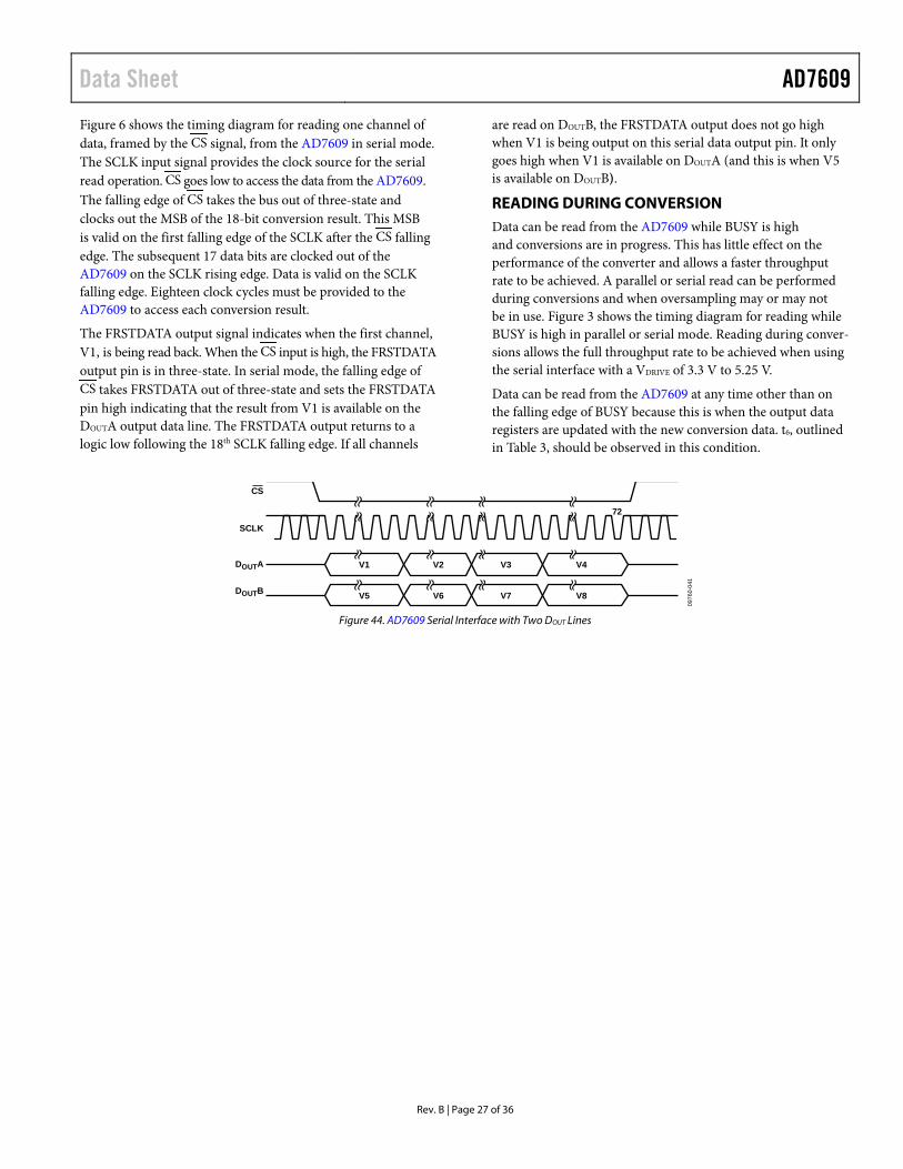
DIGITAL INTERFACE The AD7609 provides two interface options: a parallel interface and a high speed serial interface. The required interface mode is selected via the PAR/SER SEL pin.
The operation of the interface modes is described in the following sections.
PARALLEL INTERFACE (PAR/SER SEL = 0)
Data can be read from the AD7609 via the parallel data bus with standard CS and RD signals. To read the data over the parallel bus, the PAR/SER SEL pin should be tied low. The CS and RD input signals are internally gated to enable the conversion result onto the data bus. The data lines, DB15 to DB0, leave their high impedance state when both CS and RD are logic low.
The rising edge of the CS input signal three-states the bus and the falling edge of the CS input signal takes the bus out of the high impedance state. CS is the control signal that enables the data lines; it is the function that allows multiple AD7609 devices to share the same parallel data bus. The CS signal can be permanently tied low, and the RD signal can be used to access the conversion results, as shown in Figure 4. A read operation of new data can take place after the BUSY signal goes low (Figure 2), or, alternatively, a read operation of data from the previous conversion process can take place while BUSY is high (Figure 3).
The RD pin is used to read data from the output conversion results register. Two RD pulses are required to read the full 18-bit conversion result from each channel. Applying a sequence of 16 RD pulses to the AD7609 RD pin clocks the conversion results out from each channel onto the parallel output bus, DB[15:0], in ascending order. The first RD falling edge after BUSY goes low clocks out DB[17:2] of the V1 result, the next RD falling edge updates the bus with DB[1:0] of the V1 result. It takes 16 RD pulses to read the eight 18-bit conversion results from the AD7609. The 16th falling edge of RD clocks out the DB[1:0] conversion result for Channel V8. When the RD signal is logic low, it enables the data conversion result from each channel to be transferred to the digital host (DSP, FPGA).
When there is only one AD7609 in a system/board and it does not share the parallel bus, data can be read using only one control signal from the digital host. The CS and RD signals can be tied together, as shown in Figure 5. In this case, the data bus comes out of three-state on the falling edge of CS/RD. The combined CS and RD signal allows the data to be clocked out of the AD7609 and to be read by the digital host. In this case, CS is used to frame the data transfer of each data channel and 16 CS pulses are required to read the eight channels of data.
AD760914BUSY
12RD
33:16DB[15:0]
13CS
DIGITALHOST
INTERRUPT
0976
0-04
0
Figure 43. AD7609 Interface Diagram: One AD7609 Using the Parallel Bus; CS
and RD Shorted Together
SERIAL INTERFACE (PAR/SER SEL = 1)
To read data back from the AD7609 over the serial interface, the PAR/SER SEL pin should be tied high. The CS and SCLK signals are used to transfer data from the AD7609. The AD7609 has two serial data output pins, DOUTA and DOUTB. Data can be read back from the AD7609 using one or both of these DOUT lines. For the AD7609, conversion results from Channel V1 to Channel V4 first appear on DOUTA, whereas conversion results from Channel V5 to Channel V8 first appear on DOUTB.
The CS falling edge takes the data output lines (DOUTA and DOUTB) out of three-state and clocks out the MSB of the conver-sion result. The rising edge of SCLK clocks all subsequent data bits onto the serial data outputs, DOUTA and DOUTB. The CS input can be held low for the entire serial read or it can be pulsed to frame each channel read of 18 SCLK cycles.
Figure 44 shows a read of eight simultaneous conversion results using two DOUT lines on the AD7609. In this case, a 72 SCLK transfer is used to access data from the AD7609 and CS is held low to frame the entire 72 SCLK cycles. Data can also be clocked out using only one DOUT line, in which case DOUTA is recom-mended to access all conversion data, because the channel data is output in ascending order. For the AD7609 to access all eight conversion results on one DOUT line, a total of 144 SCLK cycles are required. These 144 SCLK cycles can be framed by one CS signal or each group of 18 SCLK cycles can be individually framed by the CS signal. The disadvantage of using only one DOUT line is that the throughput rate is reduced if reading after conversion. The unused DOUT line should be left unconnected in serial mode. For the AD7609, if DOUTB is to be used as a single DOUT line, the channel results are output in the following order: V5, V6, V7, V8, V1, V2, V3, V4; however, the FRSTDATA indicator returns low after V5 is read on DOUTB.
Rev. B | Page 26 of 36
Data Sheet AD7609 Figure 6 shows the timing diagram for reading one channel of data, framed by the CS signal, from the AD7609 in serial mode. The SCLK input signal provides the clock source for the serial read operation. CS goes low to access the data from the AD7609. The falling edge of CS takes the bus out of three-state and clocks out the MSB of the 18-bit conversion result. This MSB is valid on the first falling edge of the SCLK after the CS falling edge. The subsequent 17 data bits are clocked out of the AD7609 on the SCLK rising edge. Data is valid on the SCLK falling edge. Eighteen clock cycles must be provided to the AD7609 to access each conversion result.
The FRSTDATA output signal indicates when the first channel, V1, is being read back. When the CS input is high, the FRSTDATA output pin is in three-state. In serial mode, the falling edge of CS takes FRSTDATA out of three-state and sets the FRSTDATA pin high indicating that the result from V1 is available on the DOUTA output data line. The FRSTDATA output returns to a logic low following the 18th SCLK falling edge. If all channels
are read on DOUTB, the FRSTDATA output does not go high when V1 is being output on this serial data output pin. It only goes high when V1 is available on DOUTA (and this is when V5 is available on DOUTB).
READING DURING CONVERSION Data can be read from the AD7609 while BUSY is high and conversions are in progress. This has little effect on the performance of the converter and allows a faster throughput rate to be achieved. A parallel or serial read can be performed during conversions and when oversampling may or may not be in use. Figure 3 shows the timing diagram for reading while BUSY is high in parallel or serial mode. Reading during conver-sions allows the full throughput rate to be achieved when using the serial interface with a VDRIVE of 3.3 V to 5.25 V.
Data can be read from the AD7609 at any time other than on the falling edge of BUSY because this is when the output data registers are updated with the new conversion data. t6, outlined in Table 3, should be observed in this condition.
V1 V4V2 V3
V5 V8V6 V7
SCLK
DOUTA
DOUTB
CS
72
0976
0-04
1
Figure 44. AD7609 Serial Interface with Two DOUT Lines
Rev. B | Page 27 of 36
AD7609 Data Sheet
Rev. B | Page 28 of 36
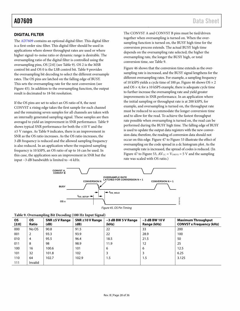
DIGITAL FILTER The AD7609 contains an optional digital filter. This digital filter is a first-order sinc filter. This digital filter should be used in applications where slower throughput rates are used or where higher signal-to-noise ratio or dynamic range is desirable. The oversampling ratio of the digital filter is controlled using the oversampling pins, OS [2:0] (see Table 9). OS 2 is the MSB control bit and OS 0 is the LSB control bit. Table 9 provides the oversampling bit decoding to select the different oversample rates. The OS pins are latched on the falling edge of BUSY. This sets the oversampling rate for the next conversion (see Figure 45). In addition to the oversampling function, the output result is decimated to 18-bit resolution.
If the OS pins are set to select an OS ratio of 8, the next CONVST x rising edge takes the first sample for each channel and the remaining seven samples for all channels are taken with an internally generated sampling signal. These samples are then averaged to yield an improvement in SNR performance. Table 9 shows typical SNR performance for both the ±10 V and the ±5 V ranges. As Table 9 indicates, there is an improvement in SNR as the OS ratio increases. As the OS ratio increases, the 3 dB frequency is reduced and the allowed sampling frequency is also reduced. In an application where the required sampling frequency is 10 kSPS, an OS ratio of up to 16 can be used. In this case, the application sees an improvement in SNR but the input −3 dB bandwidth is limited to ~6 kHz.
The CONVST A and CONVST B pins must be tied/driven together when oversampling is turned on. When the over-sampling function is turned on, the BUSY high time for the conversion process extends. The actual BUSY high time depends on the oversampling rate selected; the higher the oversampling rate, the longer the BUSY high, or total conversion time, see Table 9.
Figure 46 shows that the conversion time extends as the over-sampling rate is increased, and the BUSY signal lengthens for the different oversampling rates. For example, a sampling frequency of 10 kSPS yields a cycle time of 100 μs. Figure 46 shows OS × 2 and OS × 4; for a 10 kSPS example, there is adequate cycle time to further increase the oversampling rate and yield greater improvements in SNR performance. In an application where the initial sampling or throughput rate is at 200 kSPS, for example, and oversampling is turned on, the throughput rate must be reduced to accommodate the longer conversion time and to allow for the read. To achieve the fastest throughput rate possible when oversampling is turned on, the read can be performed during the BUSY high time. The falling edge of BUSY is used to update the output data registers with the new conver-sion data; therefore, the reading of conversion data should not occur on this edge. Figure 47 to Figure 53 illustrate the effect of oversampling on the code spread in a dc histogram plot. As the oversample rate is increased, the spread of codes is reduced. (In Figure 47 to Figure 53, AVCC = VDRIVE = 5 V and the sampling rate was scaled with OS ratio.)
CONVST A,CONVST B
BUSY
OS x
tOS_SETUP
tOS_HOLD
CONVERSION N CONVERSION N + 1OVERSAMPLE RATELATCHED FOR CONVERSION N + 1
0976
0-04
2
Figure 45. OS Pin Timing
Table 9. Oversampling Bit Decoding (100 Hz Input Signal) OS [2:0]
OS Ratio
SNR ±5 V Range (dB)
SNR ±10 V Range (dB)
−3 dB BW 5 V Range (kHz)
−3 dB BW 10 V Range (kHz)
Maximum Throughput CONVST x Frequency (kHz)
000 No OS 90.8 91.5 22 33 200 001 2 93.3 93.9 22 28.9 100 010 4 95.5 96.4 18.5 21.5 50 011 8 98 98.9 11.9 12 25 100 16 100.6 101 6 6 12.5 101 32 101.8 102 3 3 6.25 110 64 102.7 102.9 1.5 1.5 3.125 111 Invalid

Data Sheet AD7609
CS
RD
DATA:DB[15:0]
BUSY
CONVST A,CONVST B
tCYCLE
tCONV
4µs
t4t4
t4
9µs
19µs
OS = 0 OS = 2 OS = 4
0976
0-04
3
Figure 46. AD7609—No Oversampling, Oversampling × 4, and Oversampling × 8 Using Read After Conversion
0
200
400
600
800
1000
1200
1400
1600
–9 –8 –7 –6 –5 –4 –3 –2 –1 0CODE
1 2 3 4 5 6 7 8 9
NO OVERSAMPLING
NU
MB
ER O
F O
CC
UR
REN
CES
0976
0-04
4
2 10 2783
210
450
727
1062
1384 1373
1167
840
492
219
10032 11 2 1
Figure 47. Histogram of Codes—No OS (19 Codes)
0
200
400
600
800
1000
1400
1800
1200
1600
2000
–7 –6 –5 –4 –3 –2 –1 0CODE
1 2 3 4 5 6 7
OVERSAMPLING BY 2
NU
MB
ER O
F O
CC
UR
REN
CES
0976
0-04
5
1 12 46
214
599
1146
1785 1772
1389
788
317
10515 2 1
Figure 48. Histogram Of Codes—OS × 2 (15 Codes)
500
0
1000
1500
2500
2000
3000
–5 –4 –3 –2 –1 0CODE
1 2 3 4
OVERSAMPLING BY 4
NU
MB
ER O
F O
CC
UR
REN
CES
0976
0-04
6
5 49
341
1191
2363 2394
1340
422
79 8
Figure 49. Histogram of Codes—OS × 4 (10 Codes)
0
500
1000
1500
2000
2500
3000
4000
3500
–4 –3 –2 –1 0CODE
1 2 3
OVERSAMPLING BY 8
NU
MB
ER O
F O
CC
UR
REN
CES
0976
0-04
7
1 41
549
22915
1568
3392
2397
Figure 50. Histogram of Codes—OS × 8 (Eight Codes)
Rev. B | Page 29 of 36
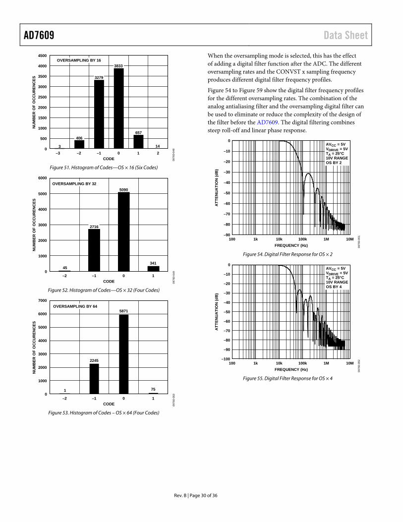
AD7609 Data Sheet
OVERSAMPLING BY 16
0
500
1000
1500
2000
3000
4000
2500
3500
4500
–2–3 –1 0CODE
1 2
385
NU
MB
ER O
F O
CC
UR
ENC
ES
0976
0-04
8
3
406
3279
3833
657
14
Figure 51. Histogram of Codes—OS × 16 (Six Codes)
45
5090
341
OVERSAMPLING BY 32
0
1000
2000
3000
4000
5000
6000
–2 –1CODE
0 1
NU
MB
ER O
F O
CC
UR
ENC
ES
0976
0-04
9
2716
Figure 52. Histogram of Codes—OS × 32 (Four Codes)
1
5871
75
OVERSAMPLING BY 64
0
1000
2000
3000
4000
6000
5000
7000
–2 –1CODE
0 1
NU
MB
ER O
F O
CC
UR
ENC
ES
0976
0-05
0
2245
Figure 53. Histogram of Codes – OS × 64 (Four Codes)
When the oversampling mode is selected, this has the effect of adding a digital filter function after the ADC. The different oversampling rates and the CONVST x sampling frequency produces different digital filter frequency profiles.
Figure 54 to Figure 59 show the digital filter frequency profiles for the different oversampling rates. The combination of the analog antialiasing filter and the oversampling digital filter can be used to eliminate or reduce the complexity of the design of the filter before the AD7609. The digital filtering combines steep roll-off and linear phase response.
0
–10
–20
–30
–40
–50
–60
–70
–80
100 1k 10k 100k 10M1M–90
ATT
ENU
ATI
ON
(dB
)
FREQUENCY (Hz)
AVCC = 5VVDRIVE = 5VTA = 25°C10V RANGEOS BY 2
0976
0-05
1
Figure 54. Digital Filter Response for OS × 2
0
–10
–20
–30
–40
–50
–60
–70
–80
100 1k 10k 100k 10M1M–100
–90
ATT
ENU
ATI
ON
(dB
)
FREQUENCY (Hz) 0976
0-05
2
AVCC = 5VVDRIVE = 5VTA = 25°C10V RANGEOS BY 4
Figure 55. Digital Filter Response for OS × 4
Rev. B | Page 30 of 36
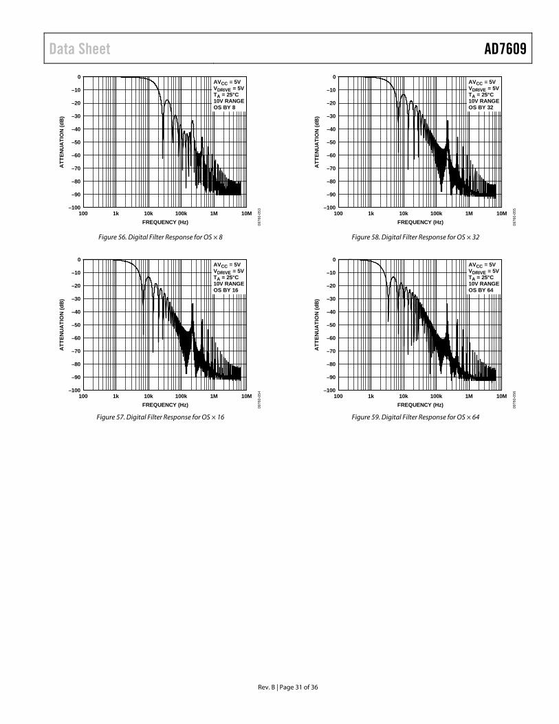
Data Sheet AD7609
0
–10
–20
–30
–40
–50
–60
–70
–80
100 1k 10k 100k 10M1M–100
–90
ATT
ENU
ATI
ON
(dB
)
FREQUENCY (Hz)
AVCC = 5VVDRIVE = 5VTA = 25°C10V RANGEOS BY 8
0976
0-05
3
Figure 56. Digital Filter Response for OS × 8
0
–10
–20
–30
–40
–50
–60
–70
–80
100 1k 10k 100k 10M1M–100
–90
ATT
ENU
ATI
ON
(dB
)
FREQUENCY (Hz)
AVCC = 5VVDRIVE = 5VTA = 25°C10V RANGEOS BY 16
0976
0-05
4
Figure 57. Digital Filter Response for OS × 16
0
–10
–20
–30
–40
–50
–60
–70
–80
100 1k 10k 100k 10M1M–100
–90
ATT
ENU
ATI
ON
(dB
)
FREQUENCY (Hz)
AVCC = 5VVDRIVE = 5VTA = 25°C10V RANGEOS BY 32
0976
0-05
5
Figure 58. Digital Filter Response for OS × 32
0
–10
–20
–30
–40
–50
–60
–70
–80
100 1k 10k 100k 10M1M–100
–90
ATT
ENU
ATI
ON
(dB
)
FREQUENCY (Hz)
AVCC = 5VVDRIVE = 5VTA = 25°C10V RANGEOS BY 64
0976
0-05
6
Figure 59. Digital Filter Response for OS × 64
Rev. B | Page 31 of 36

AD7609 Data Sheet
LAYOUT GUIDELINES The printed circuit board that houses the AD7609 should be designed so that the analog and digital sections are separated and confined to different areas of the board.
Use at least one ground plane. It can be common or split between the digital and analog sections. In the case of the split plane, the digital and analog ground planes should be joined in only one place, preferably as close as possible to the AD7609.
If the AD7609 is in a system where multiple devices require analog-to-digital ground connections, the connection should still be made at only one point, a star ground point, which should be established as close as possible to the AD7609. Good connections should be made to the ground plane. Avoid sharing one connection for multiple ground pins. Individual vias or multiple vias to the ground plane should be used for each ground pin.
Avoid running digital lines under the devices because doing so couples noise onto the die. Allow the analog ground plane to run under the AD7609 to avoid noise coupling. Shield fast-switching signals like CONVST A, CONVST B, or clocks with digital ground to avoid radiating noise to other sections of the board, and they should never run near analog signal paths. Avoid crossover of digital and analog signals. Run traces on layers in close proximity on the board at right angles to each other to reduce the effect of feedthrough through the board.
The power supply lines to the AVCC and VDRIVE pins on the AD7609 should use as large a trace as possible to provide low impedance paths and reduce the effect of glitches on the power supply lines. Where possible, use supply planes. Good connec-tions should be made between the AD7609 supply pins and the power tracks on the board; this should involve the use of a single via or multiple vias for each supply pin.
Good decoupling is also important to lower the supply imped-ance presented to the AD7609 and to reduce the magnitude of the supply spikes. Place the decoupling capacitors close to, ideally right up against, these pins and their corresponding ground pins. Place the decoupling capacitors for the REFIN/ REFOUT pin and the REFCAPA and REFCAPB pins as close as possible to their respective AD7609 pins. Where possible, they should be placed on the same side of the board as the AD7609 device. Figure 60 shows the recommended decoupling on the top layer of the AD7609 board. Figure 61 shows bottom layer decoupling. Bottom layer decoupling is for the four AVCC pins and the VDRIVE pin.
0976
0-05
7
Figure 60. Top Layer Decoupling REFIN/REFOUT, REFCAPA, REFCAPB, and
REGCAP Pins
0976
0-05
8
Figure 61. Bottom Layer Decoupling
Rev. B | Page 32 of 36
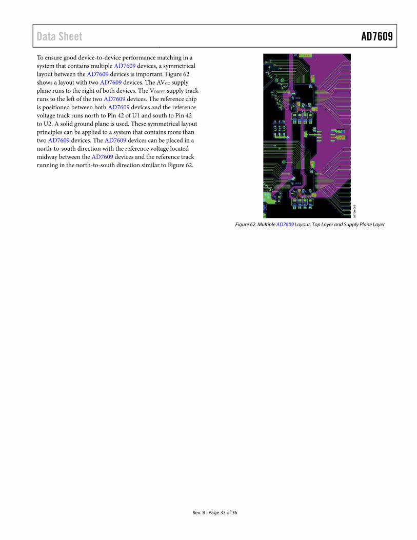
Data Sheet AD7609 To ensure good device-to-device performance matching in a system that contains multiple AD7609 devices, a symmetrical layout between the AD7609 devices is important. Figure 62 shows a layout with two AD7609 devices. The AVCC supply plane runs to the right of both devices. The VDRIVE supply track runs to the left of the two AD7609 devices. The reference chip is positioned between both AD7609 devices and the reference voltage track runs north to Pin 42 of U1 and south to Pin 42 to U2. A solid ground plane is used. These symmetrical layout principles can be applied to a system that contains more than two AD7609 devices. The AD7609 devices can be placed in a north-to-south direction with the reference voltage located midway between the AD7609 devices and the reference track running in the north-to-south direction similar to Figure 62.
0976
0-05
9
Figure 62. Multiple AD7609 Layout, Top Layer and Supply Plane Layer
Rev. B | Page 33 of 36
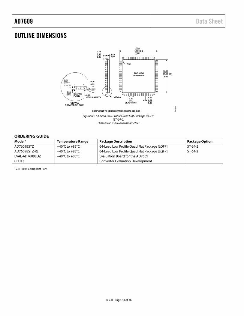
AD7609 Data Sheet
OUTLINE DIMENSIONS
COMPLIANT TO JEDEC STANDARDS MS-026-BCD 0517
06-A
TOP VIEW(PINS DOWN)
1
1617
3332
484964
0.270.220.17
0.50BSC
LEAD PITCH
12.2012.00 SQ11.80
PIN 1
1.60MAX
0.750.600.45
10.2010.00 SQ9.80
VIEW A
0.20 0.09
1.451.401.35
0.08COPLANARITY
VIEW AROTATED 90° CCW
SEATINGPLANE
0.150.05
7°3.5°0°
Figure 63. 64-Lead Low Profile Quad Flat Package [LQFP]
(ST-64-2) Dimensions shown in millimeters
ORDERING GUIDE Model1 Temperature Range Package Description Package Option AD7609BSTZ −40°C to +85°C 64-Lead Low Profile Quad Flat Package [LQFP] ST-64-2 AD7609BSTZ-RL −40°C to +85°C 64-Lead Low Profile Quad Flat Package [LQFP] ST-64-2 EVAL-AD7609EDZ −40°C to +85°C Evaluation Board for the AD7609 CED1Z Converter Evaluation Development
1 Z = RoHS Compliant Part.
Rev. B | Page 34 of 36

Data Sheet AD7609
NOTES
Rev. B | Page 35 of 36

AD7609 Data Sheet
NOTES
©2011–2014 Analog Devices, Inc. All rights reserved. Trademarks and registered trademarks are the property of their respective owners. D09760-0-5/14(B)
Rev. B | Page 36 of 36