fin1018 3.3v lvds 1-bit high speed differential...
TRANSCRIPT

© 2002 Fairchild Semiconductor Corporation DS500502 www.fairchildsemi.com
March 2001
Revised April 2002
FIN
1018 3.3V LV
DS
1-Bit H
igh
Sp
eed D
ifferential R
eceiver
FIN10183.3V LVDS 1-Bit High Speed Differential Receiver
General DescriptionThis single receiver is designed for high speed intercon-nects utilizing Low Voltage Differential Signaling (LVDS)technology. The receiver translates LVDS levels, with a typ-ical differential input threshold of 100 mV, to LVTTL signallevels. LVDS provides low EMI at ultra low power dissipa-tion even at high frequencies. This device is ideal for highspeed transfer of clock or data.
The FIN1018 can be paired with its companion driver, theFIN1017, or with any other LVDS driver.
Features■ Greater than 400Mbs data rate
■ 3.3V power supply operation
■ 0.4ns maximum pulse skew
■ 2.5ns maximum propagation delay
■ Low power dissipation
■ Power-Off protection
■ Fail safe protection for open-circuit, shorted and termi-nated conditions
■ Meets or exceeds the TIA/EIA-644 LVDS standard
■ Flow-through pinout simplifies PCB layout
■ 8-Lead SOIC and US-8 packages save space
Ordering Code:
Pin Descriptions
Function Table
H = HIGH Logic LevelL = LOW Logic LevelFail Safe = Open, Shorted, Terminated
Connection Diagrams
8-Lead SOIC
Pin Assignment for US-8 Package
TOP VIEW
Order Number Package Number Package Description
FIN1018M M08A 8-Lead Small Outline Integrated Circuit (SOIC), JEDEC MS-012, 0.150" Narrow[TUBE]
FIN1018MX M08A 8-Lead Small Outline Integrated Circuit (SOIC), JEDEC MS-012, 0.150" Narrow[TAPE and REEL]
FIN1018K8X MAB08A 8-Lead US8, JEDEC MO-187, Variation CA 3.1mm Wide[TAPE and REEL]
Pin Name Description
ROUT LVTTL Data Output
RIN+ Non-inverting Driver Input
RIN− Inverting Driver Input
VCC Power Supply
GND Ground
NC No Connect
Input Outputs
RIN+ RIN− ROUT
L H L
H L H
Fail Safe Condition H

www.fairchildsemi.com 2
FIN
1018 Absolute Maximum Ratings(Note 1) Recommended Operating
Conditions
Note 1: The “Absolute Maximum Ratings”: are those values beyond whichdamage to the device may occur. The databook specifications should bemet, without exception, to ensure that the system design is reliable over itspower supply, temperature and output/input loading variables. Fairchilddoes not recommend operation of circuits outside databook specification.
DC Electrical CharacteristicsOver supply voltage and operating temperature ranges, unless otherwise specified
Note 2: All typical values are at TA = 25°C and with VCC = 3.3V.
AC Electrical CharacteristicsOver supply voltage and operating temperature ranges, unless otherwise specified
Note 3: All typical values are at TA = 25°C and with VCC = 3.3V.
Note 4: tSK(PP) is the magnitude of the difference in propagation delay times between any specified terminals of two devices switching in the same direction
(either LOW-to-HIGH or HIGH-to-LOW) when both devices operate with the same supply voltage, same temperature, and have identical test circuits.
Supply Voltage (VCC) −0.5V to +4.6V
DC Input Voltage (RIN+, RIN−) −0.5V to +4.7V
DC Output Voltage (DOUT) −0.5V to +6V
DC Output Current (IO) 16 mA
Storage Temperature Range (TSTG) −65°C to +150°CMax Junction Temperature (TJ) 150°CLead Temperature (TL)
(Soldering, 10 seconds) 260°CESD (Human Body Model) ≥ 6500V
ESD (Bus Pins RIN−/RIN+ to GND) ≥ 9500V
ESD (Machine Model) ≥ 300V
Supply Voltage (VCC) 3.0V to 3.6V
Input Voltage (VIN) 0 to VCC
Magnitude of Differential Voltage
(|VID|) 100mV to VCC
Common-mode Input Voltage (VIC) 0.05V to 2.35V
Operating Temperature (TA) −40°C to +85°C
Symbol Parameter Test ConditionsMin Typ Max
Units(Note 2)
VTH Differential Input Threshold HIGH See Figure 1 and Table 1 100 mV
VTL Differential Input Threshold LOW See Figure 1 and Table 1 −100 mV
IIN Input Current VIN = 0V or VCC ±20 µA
II(OFF) Power-OFF Input Current VCC = 0V, VIN = 0V or 3.6V ±20 µA
VOH Output HIGH Voltage IOH = −100 µA VCC −0.2 V
IOH = −8 mA 2.4 V
VOL Output LOW Voltage IOH = 100 µA 0.2 V
IOL = 8 mA 0.5 V
VIK Input Clamp Voltage IIK = −18 mA −1.5 V
ICC Power Supply Current Inputs Open, (RIN+ = 1V and RIN− = 1.4V),7 mA
or (RIN+ = 1.4V and RIN− = 1V)
CIN Input Capacitance 4 pF
COUT Output Capacitance 6 pF
Symbol Parameter Test ConditionsMin Typ Max
Units(Note 3)
tPLH Propagation Delay LOW-to-HIGH 0.9 2.5 ns
tPHL Propagation Delay HIGH-to-LOW 0.9 2.5 ns
tTLH Output Rise Time (20% to 80%) |VID| = 400 mV, CL = 10 pF 0.5 ns
tTHL Output Fall Time (80% to 20%) See Figure 1 and Figure 2 0.5 ns
tSK(P) Pulse Skew |tPLH - tPHL| 0.4 ns
tSK(PP) Part-to-Part Skew (Note 4) 1.0 ns
3 www.fairchildsemi.com
FIN
1018
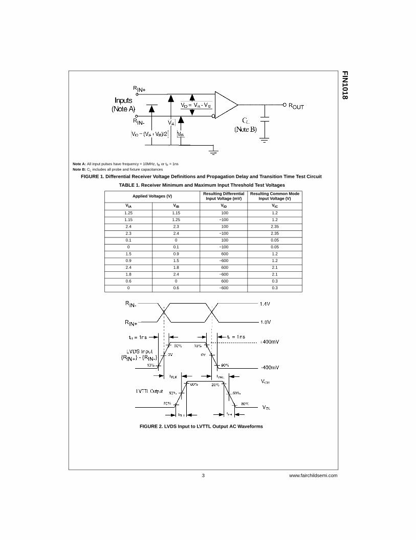
Note A: All input pulses have frequency = 10MHz, tR or tF = 1ns
Note B: CL includes all probe and fixture capacitances
FIGURE 1. Differential Receiver Voltage Definitions and Propagation Delay and Transition Time Test Circuit
TABLE 1. Receiver Minimum and Maximum Input Threshold Test Voltages
FIGURE 2. LVDS Input to LVTTL Output AC Waveforms
Applied Voltages (V)Resulting Differential
Input Voltage (mV)Resulting Common Mode
Input Voltage (V)
VIA VIB VID VIC
1.25 1.15 100 1.2
1.15 1.25 −100 1.2
2.4 2.3 100 2.35
2.3 2.4 −100 2.35
0.1 0 100 0.05
0 0.1 −100 0.05
1.5 0.9 600 1.2
0.9 1.5 −600 1.2
2.4 1.8 600 2.1
1.8 2.4 −600 2.1
0.6 0 600 0.3
0 0.6 −600 0.3

www.fairchildsemi.com 4
FIN
1018 DC / AC Typical Performance Curves
FIGURE 3. Output High Voltage vs.Power Supply Voltage
FIGURE 4. Output Low Voltage vs.Power Supply Voltage
FIGURE 5. Output Short Circuit Current vs.Power Supply Voltage
FIGURE 6. Power Supply Current vs.Frequency
FIGURE 7. Power Supply Current vs.Ambient Temperature
FIGURE 8. Differential Propagation Delay Power Supply Voltage
5 www.fairchildsemi.com
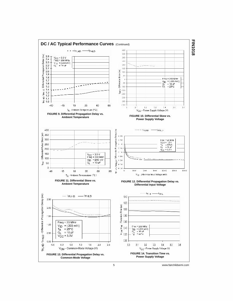
FIN
1018DC / AC Typical Performance Curves (Continued)
FIGURE 9. Differential Propagation Delay vs.Ambient Temperature FIGURE 10. Differential Skew vs.
Power Supply Voltage
FIGURE 11. Differential Skew vs.Ambient Temperature
FIGURE 12. Differential Propagation Delay vs.Differential Input Voltage
FIGURE 13. Differential Propagation Delay vs.Common-Mode Voltage
FIGURE 14. Transition Time vs.Power Supply Voltage
www.fairchildsemi.com 6
FIN
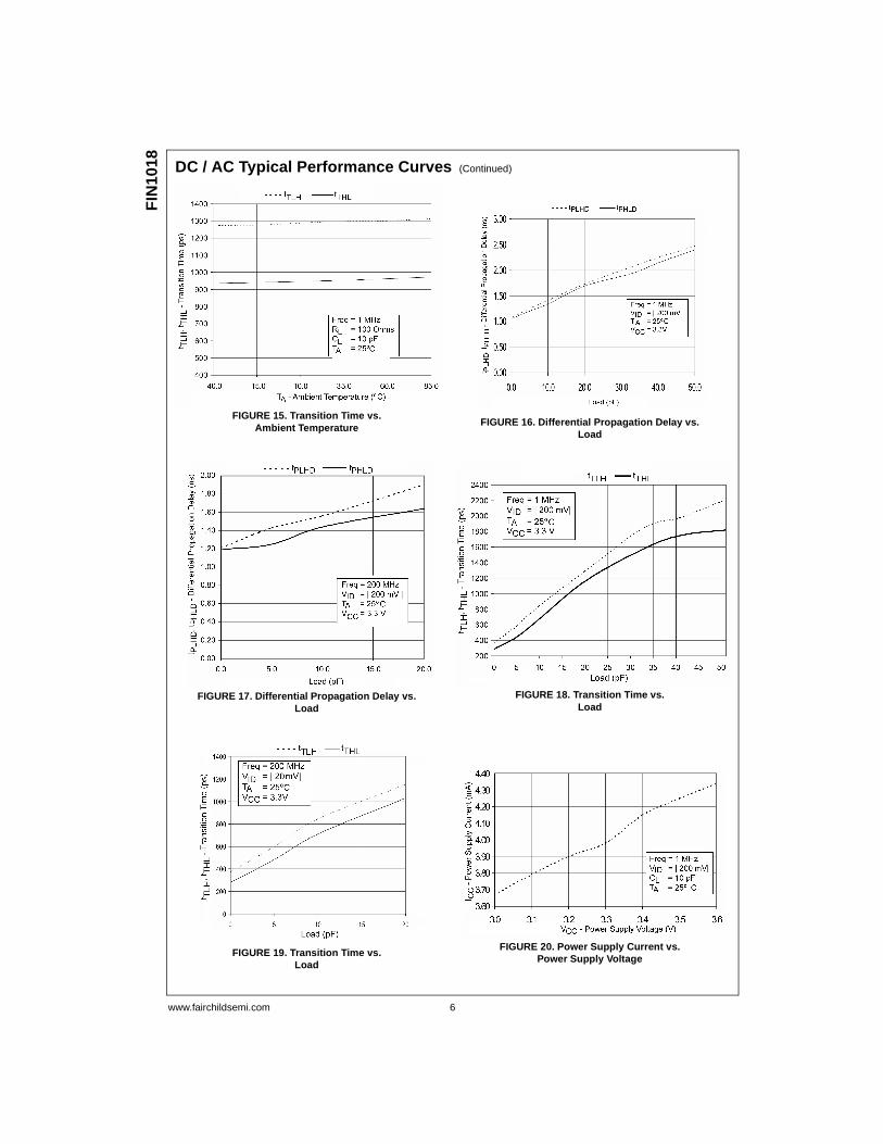
1018 DC / AC Typical Performance Curves (Continued)
FIGURE 15. Transition Time vs.Ambient Temperature FIGURE 16. Differential Propagation Delay vs.
Load
FIGURE 17. Differential Propagation Delay vs.Load
FIGURE 18. Transition Time vs. Load
FIGURE 19. Transition Time vs.Load
FIGURE 20. Power Supply Current vs.Power Supply Voltage
7 www.fairchildsemi.com
FIN
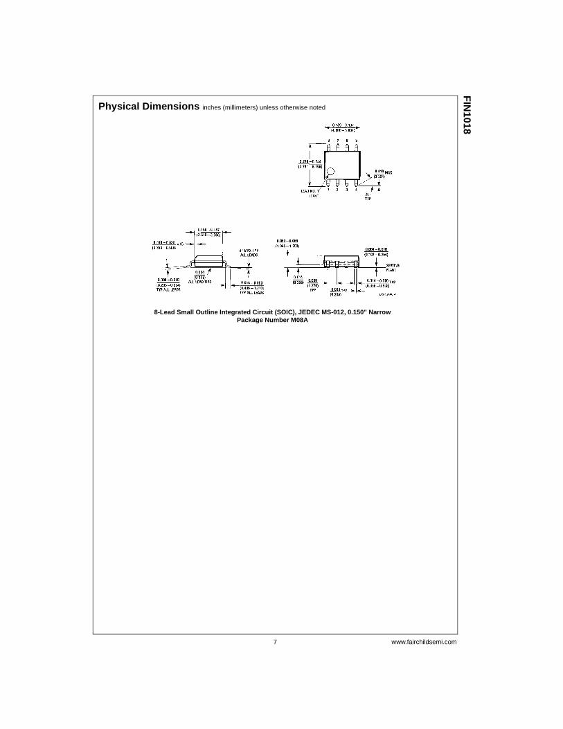
1018Physical Dimensions inches (millimeters) unless otherwise noted
8-Lead Small Outline Integrated Circuit (SOIC), JEDEC MS-012, 0.150" NarrowPackage Number M08A

www.fairchildsemi.com 8
FIN
1018
3.3
V L
VD
S 1
-Bit
Hig
h S
pee
d D
iffe
ren
tial
Rec
eive
rPhysical Dimensions inches (millimeters) unless otherwise noted (Continued)
8-Lead US8, JEDEC MO-187, Variation CA 3.1mm WidePackage Number MAB08A
Fairchild does not assume any responsibility for use of any circuitry described, no circuit patent licenses are implied andFairchild reserves the right at any time without notice to change said circuitry and specifications.
LIFE SUPPORT POLICY
FAIRCHILD’S PRODUCTS ARE NOT AUTHORIZED FOR USE AS CRITICAL COMPONENTS IN LIFE SUPPORTDEVICES OR SYSTEMS WITHOUT THE EXPRESS WRITTEN APPROVAL OF THE PRESIDENT OF FAIRCHILDSEMICONDUCTOR CORPORATION. As used herein:
1. Life support devices or systems are devices or systemswhich, (a) are intended for surgical implant into thebody, or (b) support or sustain life, and (c) whose failureto perform when properly used in accordance withinstructions for use provided in the labeling, can be rea-sonably expected to result in a significant injury to theuser.
2. A critical component in any component of a life supportdevice or system whose failure to perform can be rea-sonably expected to cause the failure of the life supportdevice or system, or to affect its safety or effectiveness.
www.fairchildsemi.com