fin1027 / fin1027a 3.3v lvds, 2-bit, high-speed
TRANSCRIPT
April 2009
© 2001 Fairchild Semiconductor Corporation www.fairchildsemi.com FIN1027 / FIN1027 • Rev. 1.0.3
FIN1027 / FIN
1027A —
3.3V LVDS, 2-B
it, High-Speed, D
ifferential Driver
FIN1027 / FIN1027A — 3.3V LVDS, 2-Bit, High-Speed, Differential Driver
Features Greater than 600Mbs Data Rate
3V Power Supply Operation
5ns Maximum Differential Pulse Skew
1.5ns Maximum Propagation Delay
Low Power Dissipation
Power-Off Protection
Meets or Exceeds the TIA/EIA-644 LVDS Standard
Flow-through Pinout Simplifies PCB Layout
Description This dual driver is designed for high-speed interconnects utilizing Low Voltage Differential Signaling (LVDS) technology. The driver translates LVTTL signal levels to LVDS levels with a typical differential output swing of 350mV, which provides low EMI at ultra-low power dissipation, even at high frequencies. This device is ideal for high-speed transfer of clock or data.
The FIN1027 or FIN1027A can be paired with its companion receiver, the FIN1028, or with any other LVDS receiver.
Ordering Information
Part Number Operating Temperature Range Eco Status Package Packing
Method
FIN1027M -40 to +85°C Green 8-Lead Small Outline Package (SOIC) JEDEC MS-012, 0.150 inch Narrow Trays
FIN1027MX -40 to +85°C Green 8-Lead Small Outline Package (SOIC) JEDEC MS-012, 0.150 inch Narrow Tape and Reel
FIN1027K8X -40 to +85°C RoHS 8-Lead US8, JEDEC MO-187, Variation CA 3.1mm Wide Tape and Reel
FIN1027AMX -40 to +85°C Green 8-Lead Small Outline Package (SOIC) JEDEC MS-012, 0.150 inch Narrow Tape and Reel
For Fairchild’s definition of Eco Status, please visit: http://www.fairchildsemi.com/company/green/rohs_green.html.
© 2001 Fairchild Semiconductor Corporation www.fairchildsemi.com FIN1027 / FIN1027A • Rev. 1.0.3 2
FIN1027 / FIN
1027A —
3.3V LVDS, 2-B
it, High-Speed, D
ifferential Driver
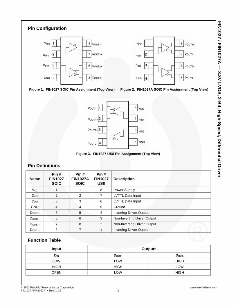
Pin Configuration
Figure 1. FIN1027 SOIC Pin Assignment (Top View) Figure 2. FIN1027A SOIC Pin Assignment (Top View)
Figure 3. FIN1027 US8 Pin Assignment (Top View)
Pin Definitions
Name Pin #
FIN1027 SOIC
Pin # FIN1027A
SOIC
Pin # FIN1027
US8 Description
VCC 1 1 8 Power Supply DIN1 2 2 7 LVTTL Data Input DIN2 3 3 6 LVTTL Data Input GND 4 4 5 Ground DOUT2- 5 5 4 Inverting Driver Output DOUT2+ 6 6 3 Non-Inverting Driver Output DOUT1+ 7 8 2 Non-Inverting Driver Output DOUT1- 8 7 1 Inverting Driver Output
Function Table
Input Outputs DIN DOUT+ DOUT-
LOW LOW HIGH HIGH HIGH LOW OPEN LOW HIGH
© 2001 Fairchild Semiconductor Corporation www.fairchildsemi.com FIN1027 / FIN1027A • Rev. 1.0.3 3
FIN1027 / FIN
1027A —
3.3V LVDS, 2-B
it, High-Speed, D
ifferential Driver
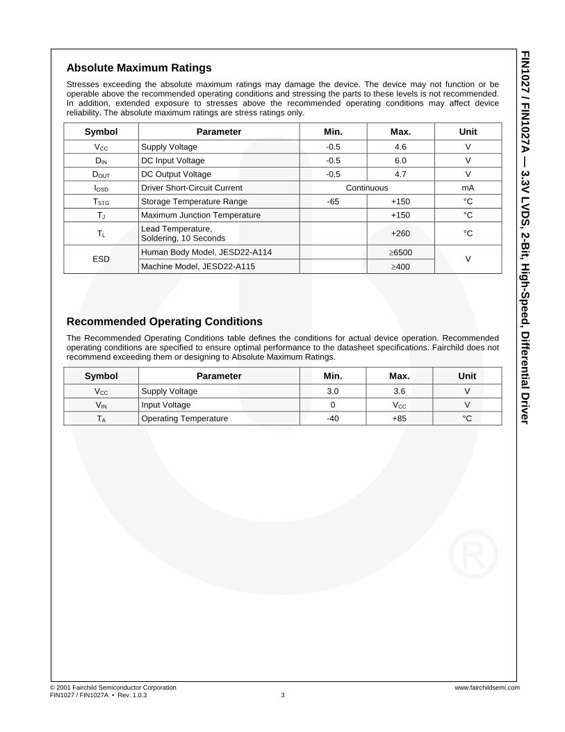
Absolute Maximum Ratings Stresses exceeding the absolute maximum ratings may damage the device. The device may not function or be operable above the recommended operating conditions and stressing the parts to these levels is not recommended. In addition, extended exposure to stresses above the recommended operating conditions may affect device reliability. The absolute maximum ratings are stress ratings only.
Symbol Parameter Min. Max. Unit VCC Supply Voltage -0.5 4.6 V DIN DC Input Voltage -0.5 6.0 V
DOUT DC Output Voltage -0.5 4.7 V IOSD Driver Short-Circuit Current Continuous mA TSTG Storage Temperature Range -65 +150 °C TJ Maximum Junction Temperature +150 °C
TL Lead Temperature, Soldering, 10 Seconds +260 °C
Human Body Model, JESD22-A114 ≥6500 ESD
Machine Model, JESD22-A115 ≥400 V
Recommended Operating Conditions The Recommended Operating Conditions table defines the conditions for actual device operation. Recommended operating conditions are specified to ensure optimal performance to the datasheet specifications. Fairchild does not recommend exceeding them or designing to Absolute Maximum Ratings.
Symbol Parameter Min. Max. Unit VCC Supply Voltage 3.0 3.6 V VIN Input Voltage 0 VCC V TA Operating Temperature -40 +85 °C
© 2001 Fairchild Semiconductor Corporation www.fairchildsemi.com FIN1027 / FIN1027A • Rev. 1.0.3 4
FIN1027 / FIN
1027A —
3.3V LVDS, 2-B
it, High-Speed, D
ifferential Driver
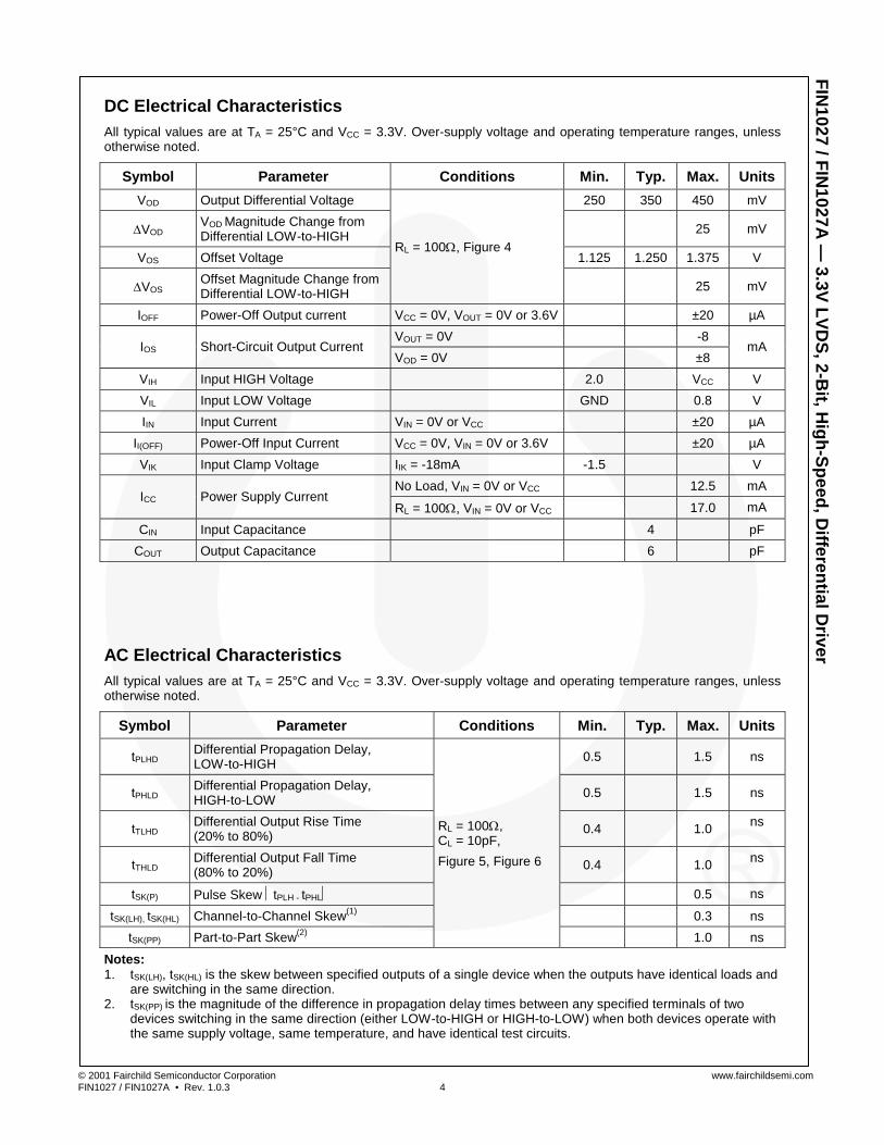
DC Electrical Characteristics All typical values are at TA = 25°C and VCC = 3.3V. Over-supply voltage and operating temperature ranges, unless otherwise noted.
Symbol Parameter Conditions Min. Typ. Max. Units VOD Output Differential Voltage 250 350 450 mV
ΔVOD VOD Magnitude Change from Differential LOW-to-HIGH 25 mV
VOS Offset Voltage 1.125 1.250 1.375 V
ΔVOS Offset Magnitude Change from Differential LOW-to-HIGH
RL = 100Ω, Figure 4
25 mV
IOFF Power-Off Output current VCC = 0V, VOUT = 0V or 3.6V ±20 µA VOUT = 0V -8
IOS Short-Circuit Output Current VOD = 0V ±8
mA
VIH Input HIGH Voltage 2.0 VCC V VIL Input LOW Voltage GND 0.8 V IIN Input Current VIN = 0V or VCC ±20 µA
II(OFF) Power-Off Input Current VCC = 0V, VIN = 0V or 3.6V ±20 µA VIK Input Clamp Voltage IIK = -18mA -1.5 V
No Load, VIN = 0V or VCC 12.5 mA ICC Power Supply Current
RL = 100Ω, VIN = 0V or VCC 17.0 mA
CIN Input Capacitance 4 pF COUT Output Capacitance 6 pF
AC Electrical Characteristics All typical values are at TA = 25°C and VCC = 3.3V. Over-supply voltage and operating temperature ranges, unless otherwise noted.
Symbol Parameter Conditions Min. Typ. Max. Units
tPLHD Differential Propagation Delay, LOW-to-HIGH 0.5 1.5 ns
tPHLD Differential Propagation Delay, HIGH-to-LOW 0.5 1.5 ns
tTLHD Differential Output Rise Time (20% to 80%) 0.4 1.0 ns
tTHLD Differential Output Fall Time (80% to 20%) 0.4 1.0 ns
tSK(P) Pulse Skew ⏐tPLH - tPHL⏐ 0.5 ns
tSK(LH), tSK(HL) Channel-to-Channel Skew(1) 0.3 ns tSK(PP) Part-to-Part Skew(2)
RL = 100Ω, CL = 10pF, Figure 5, Figure 6
1.0 ns
Notes: 1. tSK(LH), tSK(HL) is the skew between specified outputs of a single device when the outputs have identical loads and
are switching in the same direction. 2. tSK(PP) is the magnitude of the difference in propagation delay times between any specified terminals of two
devices switching in the same direction (either LOW-to-HIGH or HIGH-to-LOW) when both devices operate with the same supply voltage, same temperature, and have identical test circuits.
© 2001 Fairchild Semiconductor Corporation www.fairchildsemi.com FIN1027 / FIN1027A • Rev. 1.0.3 5
FIN1027 / FIN
1027A —
3.3V LVDS, 2-B
it, High-Speed, D
ifferential Driver
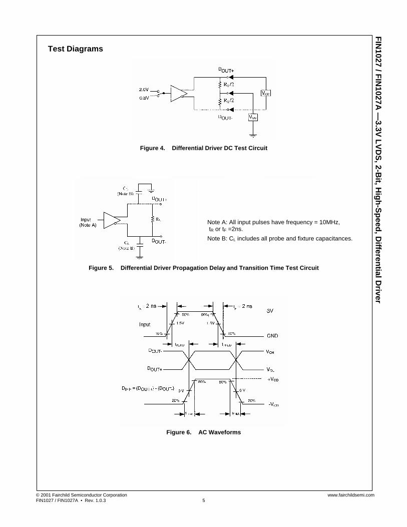
Test Diagrams
Figure 4. Differential Driver DC Test Circuit
Note A: All input pulses have frequency = 10MHz, tR or tF =2ns. Note B: CL includes all probe and fixture capacitances.
Figure 5. Differential Driver Propagation Delay and Transition Time Test Circuit
Figure 6. AC Waveforms
© 2001 Fairchild Semiconductor Corporation www.fairchildsemi.com FIN1027 / FIN1027A • Rev. 1.0.3 6
FIN1027 / FIN
1027A —
3.3V LVDS, 2-B
it, High-Speed, D
ifferential Driver
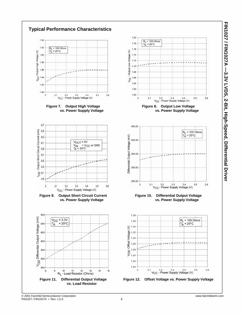
Typical Performance Characteristics
Figure 7. Output High Voltage
vs. Power Supply Voltage Figure 8. Output Low Voltage
vs. Power Supply Voltage
Figure 9. Output Short Circuit Current
vs. Power Supply Voltage Figure 10. Differential Output Voltage
vs. Power Supply Voltage
Figure 11. Differential Output Voltage
vs. Load Resistor Figure 12. Offset Voltage vs. Power Supply Voltage
© 2001 Fairchild Semiconductor Corporation www.fairchildsemi.com FIN1027 / FIN1027A • Rev. 1.0.3 7
FIN1027 / FIN
1027A —
3.3V LVDS, 2-B
it, High-Speed, D
ifferential Driver
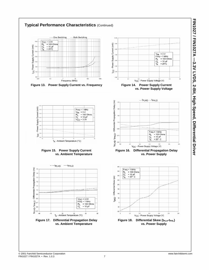
Typical Performance Characteristics (Continued)
Figure 13. Power Supply Current vs. Frequency Figure 14. Power Supply Current
vs. Power Supply Voltage
Figure 15. Power Supply Current vs. Ambient Temperature
Figure 16. Differential Propagation Delay vs. Power Supply
Figure 17. Differential Propagation Delay
vs. Ambient Temperature Figure 18. Differential Skew (tPLH-tPHL)
vs. Power Supply

© 2001 Fairchild Semiconductor Corporation www.fairchildsemi.com FIN1027 / FIN1027A • Rev. 1.0.3 8
FIN1027 / FIN
1027A —
3.3V LVDS, 2-B
it, High-Speed, D
ifferential Driver
Typical Performance Characteristics (Continued)
Figure 19. Differential Pulse Skew (tPLH-tPHL)
Figure 20. Transition Time vs. Power Supply Voltage
Figure 21. Transition Time vs. Ambient Temperature
© 2001 Fairchild Semiconductor Corporation www.fairchildsemi.com FIN1027 / FIN1027A • Rev. 1.0.3 9
FIN1027 / FIN
1027A —
3.3V LVDS, 2-B
it, High-Speed, D
ifferential Driver
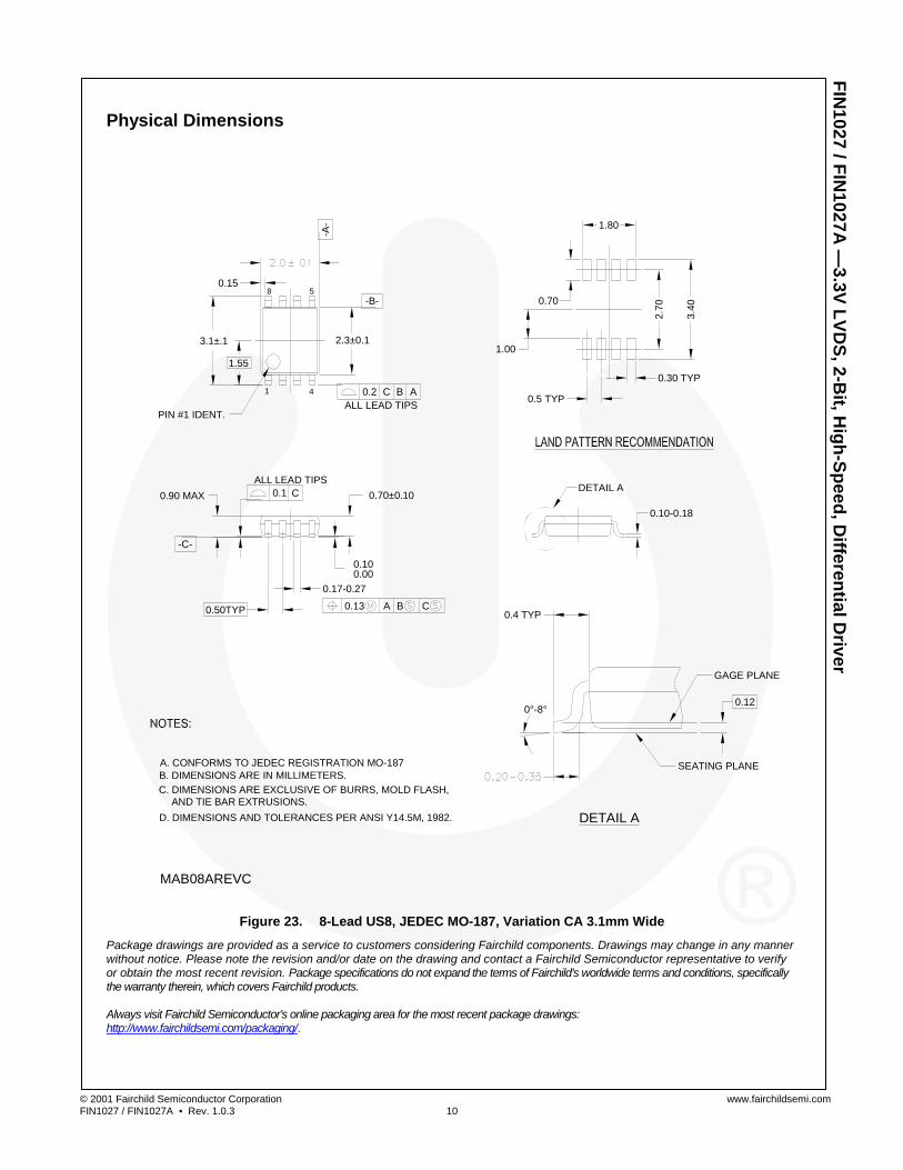
Physical Dimensions
8°0°
SEE DETAIL A
NOTES: UNLESS OTHERWISE SPECIFIED
A) THIS PACKAGE CONFORMS TO JEDEC MS-012, VARIATION AA, ISSUE C, B) ALL DIMENSIONS ARE IN MILLIMETERS. C) DIMENSIONS DO NOT INCLUDE MOLD FLASH OR BURRS. D) LANDPATTERN STANDARD: SOIC127P600X175-8M. E) DRAWING FILENAME: M08AREV13
LAND PATTERN RECOMMENDATION
SEATING PLANE
0.10 C
C
GAGE PLANE
x 45°
DETAIL ASCALE: 2:1
PIN ONEINDICATOR
4
8
1
CM B A0.25
B5
A
5.60
0.65
1.75
1.27
6.205.80
3.81
4.003.80
5.004.80
(0.33)1.27
0.510.33
0.250.10
1.75 MAX0.250.19
0.36
0.500.25R0.10
R0.10
0.900.406 (1.04)
OPTION A - BEVEL EDGE
OPTION B - NO BEVEL EDGE
Figure 22. 8-Lead, Small Outline Package (SOIC), JEDEC MS-012, 0.150-inch, Narrow Body
Click here for tape and reel specifications, available at:
http://www.fairchildsemi.com/products/discrete/pdf/soic8_tr.pdf Package drawings are provided as a service to customers considering Fairchild components. Drawings may change in any manner without notice. Please note the revision and/or date on the drawing and contact a Fairchild Semiconductor representative to verify or obtain the most recent revision. Package specifications do not expand the terms of Fairchild’s worldwide terms and conditions, specifically the warranty therein, which covers Fairchild products. Always visit Fairchild Semiconductor’s online packaging area for the most recent package drawings: http://www.fairchildsemi.com/packaging/.
© 2001 Fairchild Semiconductor Corporation www.fairchildsemi.com FIN1027 / FIN1027A • Rev. 1.0.3 10
FIN1027 / FIN
1027A —
3.3V LVDS, 2-B
it, High-Speed, D
ifferential Driver
Physical Dimensions
0.30 TYP
SEATING PLANE
0.10-0.18
0.13 A B C
C. DIMENSIONS ARE EXCLUSIVE OF BURRS, MOLD FLASH,
D. DIMENSIONS AND TOLERANCES PER ANSI Y14.5M, 1982. AND TIE BAR EXTRUSIONS.
MAB08AREVC
0.50TYP
B. DIMENSIONS ARE IN MILLIMETERS. A. CONFORMS TO JEDEC REGISTRATION MO-187
-C-
0.17-0.27
0.100.00
DETAIL A
0°-8°
0.4 TYP
-B-
0.70±0.10
ALL LEAD TIPS0.2 C B A
3.1±.1
0.15
PIN #1 IDENT.
0.90 MAXALL LEAD TIPS
0.1 C
1.55
8
1 4
2.3±0.1
5
-A-
0.70
2.70
3.40
1.00
0.5 TYP
DETAIL A
1.80
GAGE PLANE
0.12
Figure 23. 8-Lead US8, JEDEC MO-187, Variation CA 3.1mm Wide
Package drawings are provided as a service to customers considering Fairchild components. Drawings may change in any manner without notice. Please note the revision and/or date on the drawing and contact a Fairchild Semiconductor representative to verify or obtain the most recent revision. Package specifications do not expand the terms of Fairchild’s worldwide terms and conditions, specifically the warranty therein, which covers Fairchild products. Always visit Fairchild Semiconductor’s online packaging area for the most recent package drawings: http://www.fairchildsemi.com/packaging/.
© 2001 Fairchild Semiconductor Corporation www.fairchildsemi.com FIN1027 / FIN1027A • Rev. 1.0.3 11
FIN1027 / FIN
1027A —
3.3V LVDS, 2-B
it, High-Speed, D
ifferential Driver
Mouser Electronics
Authorized Distributor
Click to View Pricing, Inventory, Delivery & Lifecycle Information: Fairchild Semiconductor:
FIN1027MX FIN1027M