80 technical focus: iii-vs on silicon — optoelectronics ... · silicon photonics offers prospects...
TRANSCRIPT
The rise of cloud and other ‘big data’ services hasincreased the need to transfer information overlarger distances to link up otherwise ‘stranded’
computing capacity — an application for which light isa far better carrier than charge. In free space, light has carried information from almost
the time of the big bang, the beginning of time itself.On planet Earth, data carried by photons through fibersand other materials does require some refreshment, butfar less often than would be needed by electronic-basedcarriage.The key challenge is to integrate optical data transfer
with data processing electronics. In particular, emittersand detectors are the vital interface between siliconelectronics and optical systems.Silicon photonics offers prospects for such integration
and a number of companies already have productssampling and in ‘mass production’. However, the integ-ration is somewhat incomplete in the area of providinglaser or some other light power into the system. This isusually piped in from outside using fibers, althoughthere are increased possibilities for integrating laserchips more closely into the silicon photonics usingwafer- or chip-bonding. However, these techniquessuffer from problems such as implementing precisealignment, which adds complexity and expense.The problem is that the III-V compound semiconductor
materials favored for light emission (and detection)don’t mix well with silicon. Challenges include mis-matching of the lattice structure and poisoning of silicon electronics since the III and V groups of theperiodic table are the ones used for doping silicon forp- and n-type conduction, respectively.Direct integration of III-V materials on silicon should
reduce process complexity and cost, but lattice mis-matching reduces material quality and reduces thepossibilities for efficient light emission, particularly forlasers. Although there have been few explicit reports ofcross-fertilization up to now, there could in the futurebe transfer of expertise between those working onphotonics and III-V high-mobility transistors, wheresimilar integration problems have been raised.
While direct growth of III-V materials on silicon wouldbe desirable, wafer bonding is often more practical atthe present stage of technical development.The light used by silicon photonics is generally in the
infrared region, being restricted by the silicon trans-parency window and energy bandgap to wavelengthsabove 1.1μm. This window covers the common opticalcommunications wavelengths around 1.55μm. The substrates for such work are commonly silicon on
insulator. The high refractive index of 3.5 optically confines light by total internal reflection, allowingmicroscopic waveguides to be created.Waveguide paths for infrared light need less extreme
pattern definition of the order of a micron rather thanthe (tens of) nanometers of bleeding-edge electronics.This could give new life to processing facilities thatwould otherwise be due for running down and eventualclosure. Intel says that it has been developing silicon photonics
for 16 years — in other words the inception came atthe crescendo of the dotcom boom–bust and the subsequent cold dark years for optical networkingdevelopment.Prospects for silicon photonic optoelectronic integ-
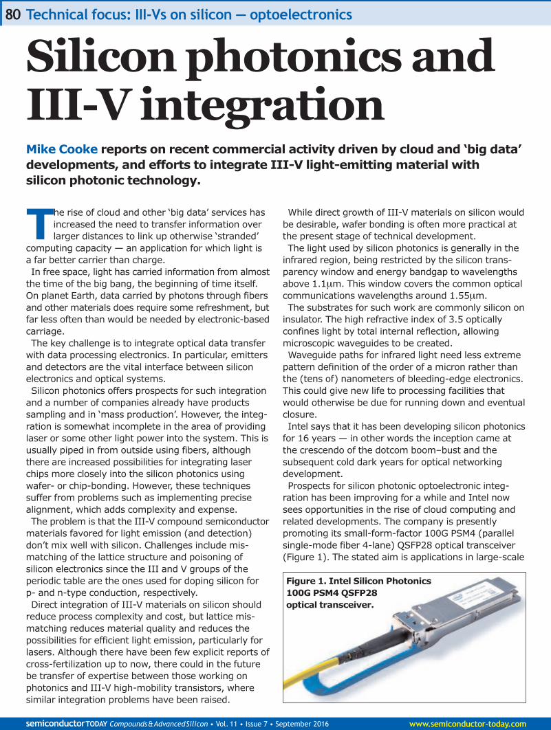
ration has been improving for a while and Intel nowsees opportunities in the rise of cloud computing andrelated developments. The company is presently promoting its small-form-factor 100G PSM4 (parallelsingle-mode fiber 4-lane) QSFP28 optical transceiver(Figure 1). The stated aim is applications in large-scale
Technical focus: III-Vs on silicon — optoelectronics
semiconductorTODAY Compounds&AdvancedSilicon • Vol. 11 • Issue 7 • September 2016 www.semiconductor-today.com
80
Mike Cooke reports on recent commercial activity driven by cloud and ‘big data’developments, and efforts to integrate III-V light-emitting material with silicon photonic technology.
Silicon photonics andIII-V integration
Figure 1. Intel Silicon Photonics100G PSM4 QSFP28 optical transceiver.
cloud and enterprise data centers, along withEthernet switch, router, andclient-side telecom inter-faces. The specification isfor 100 Gigabit [per second]Ethernet (100GbE) opticallinks over single-modefiber. Originally due in 2015, but
delayed due to unspecifieddifficulties, Intel now says that the product is“shipping in volume”. Thetransceiver incorporatesIntel’s hybrid laser technol-ogy that allows greater than90% coupling efficiency.Combined with high-densityoptical interconnects andIntel’s “unmatched manu-facturing capabilities”, thetechnology should deliverscaling and cost benefits.The reach of the device is
up to 2km, beyond thatrequired by the PSM4multi-source agreementoptical interface specifi-cation (www.psm4.org).The operating temperaturerange is 0ºC to 70ºC. Power consumption is ratedat 3.5W maximum.Beyond this specific device, Intel plans to move from
pluggable to near-future embedded products at 400G,and towards integrating optical interconnects directlyinto switch and server electronics. Intel’s roadmap alsoincludes integrated optical application specific circuits(ASICs).Intel has developed its hybrid silicon laser technology
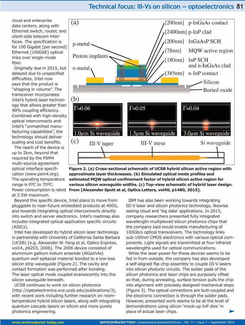
in partnership with University of California Santa Barbara(UCSB) [e.g. Alexander W. Fang et al, Optics Express,vol14, p9203, 2006]. The 2006 device consisted ofaluminium gallium indium arsenide (AlGaInAs) quantum well epitaxial material bonded to a low-losssilicon strip waveguide (Figure 2). The cavity and contact formation was performed after bonding. The laser optical mode coupled evanescently into thesilicon waveguide beneath.UCSB continues to work on silicon photonics
(http://optoelectronics.ece.ucsb.edu/publications/3),with recent work including further research on room-temperature hybrid silicon lasers, along with integratingquantum cascade lasers on silicon and more purelyphotonics engineering.
IBM has also been working towards integrating III-V laser and silicon photonics technology, likewiseseeing cloud and ‘big data’ applications. In 2015, company researchers presented fully integrated wavelength-multiplexed silicon photonics chips thatthe company said would enable manufacturing of100Gb/s optical transceivers. The technology linkssub-100nm CMOS electronics with various optical com-ponents. Light signals are transmitted at four infraredwavelengths used for optical communications.While the laser power for these devices seems to be
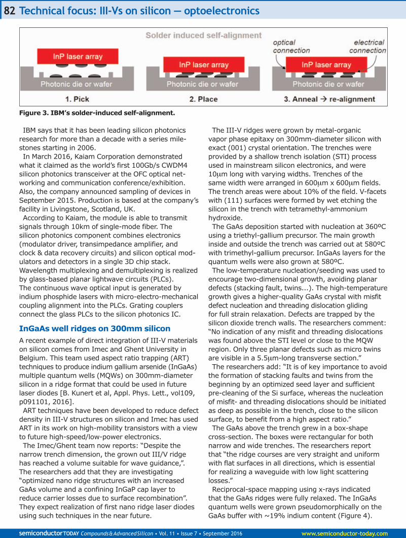
fed in from outside, the company has also developed a self-aligned flip-chip assembly to couple III-V lasersinto silicon photonic circuits. The solder pads of the silicon photonics and laser chips are purposely offsetso that, during annealing, surface tension pulls the chipinto alignment with precisely designed mechanical stops(Figure 3). The optical connections are butt-coupled andthe electronic connection is through the solder pads.However, presented work seems to be at the level ofdemonstrations using silicon ‘mock-up InP dies’ inplace of actual laser chips.
Technical focus: III-Vs on silicon — optoelectronics
www.semiconductor-today.com semiconductorTODAY Compounds&AdvancedSilicon • Vol. 11 • Issue 7 • September 2016
81
Figure 2. (a) Cross-sectional schematic of UCSB hybrid silicon active region withapproximate layer thicknesses. (b) Simulated optical mode profiles andestimated MQW optical confinement factor of hybrid silicon active region forvarious silicon waveguide widths. (c) Top-view schematic of hybrid laser design.From [Alexander Spott et al, Optics Letters, vol40, p1480, 2015].
IBM says that it has been leading silicon photonicsresearch for more than a decade with a series mile-stones starting in 2006.In March 2016, Kaiam Corporation demonstrated
what it claimed as the world’s first 100Gb/s CWDM4silicon photonics transceiver at the OFC optical net-working and communication conference/exhibition.Also, the company announced sampling of devices inSeptember 2015. Production is based at the company’sfacility in Livingstone, Scotland, UK.According to Kaiam, the module is able to transmit
signals through 10km of single-mode fiber. The silicon photonics component combines electronics(modulator driver, transimpedance amplifier, and clock & data recovery circuits) and silicon optical mod-ulators and detectors in a single 3D chip stack. Wavelength multiplexing and demultiplexing is realizedby glass-based planar lightwave circuits (PLCs). The continuous wave optical input is generated byindium phosphide lasers with micro-electro-mechanicalcoupling alignment into the PLCs. Grating couplersconnect the glass PLCs to the silicon photonics IC.
InGaAs well ridges on 300mm siliconA recent example of direct integration of III-V materialson silicon comes from Imec and Ghent University inBelgium. This team used aspect ratio trapping (ART)techniques to produce indium gallium arsenide (InGaAs)multiple quantum wells (MQWs) on 300mm-diametersilicon in a ridge format that could be used in futurelaser diodes [B. Kunert et al, Appl. Phys. Lett., vol109,p091101, 2016].ART techniques have been developed to reduce defect
density in III-V structures on silicon and Imec has usedART in its work on high-mobility transistors with a viewto future high-speed/low-power electronics.The Imec/Ghent team now reports: “Despite the
narrow trench dimension, the grown out III/V ridgehas reached a volume suitable for wave guidance,”.The researchers add that they are investigating “optimized nano ridge structures with an increasedGaAs volume and a confining InGaP cap layer toreduce carrier losses due to surface recombination”.They expect realization of first nano ridge laser diodesusing such techniques in the near future.
The III-V ridges were grown by metal-organic vapor phase epitaxy on 300mm-diameter silicon withexact (001) crystal orientation. The trenches were provided by a shallow trench isolation (STI) processused in mainstream silicon electronics, and were 10μm long with varying widths. Trenches of the same width were arranged in 600μm x 600μm fields.The trench areas were about 10% of the field. V-facetswith (111) surfaces were formed by wet etching thesilicon in the trench with tetramethyl-ammoniumhydroxide.The GaAs deposition started with nucleation at 360ºC
using a triethyl-gallium precursor. The main growthinside and outside the trench was carried out at 580ºCwith trimethyl-gallium precursor. InGaAs layers for thequantum wells were also grown at 580ºC. The low-temperature nucleation/seeding was used to
encourage two-dimensional growth, avoiding planardefects (stacking fault, twins...). The high-temperaturegrowth gives a higher-quality GaAs crystal with misfitdefect nucleation and threading dislocation gliding for full strain relaxation. Defects are trapped by the silicon dioxide trench walls. The researchers comment:“No indication of any misfit and threading dislocationswas found above the STI level or close to the MQWregion. Only three planar defects such as micro twinsare visible in a 5.5μm-long transverse section.” The researchers add: “It is of key importance to avoid
the formation of stacking faults and twins from thebeginning by an optimized seed layer and sufficientpre-cleaning of the Si surface, whereas the nucleationof misfit- and threading dislocations should be initiatedas deep as possible in the trench, close to the siliconsurface, to benefit from a high aspect ratio.”The GaAs above the trench grew in a box-shape
cross-section. The boxes were rectangular for bothnarrow and wide trenches. The researchers report that “the ridge courses are very straight and uniformwith flat surfaces in all directions, which is essential for realizing a waveguide with low light scatteringlosses.”Reciprocal-space mapping using x-rays indicated
that the GaAs ridges were fully relaxed. The InGaAsquantum wells were grown pseudomorphically on theGaAs buffer with ~19% indium content (Figure 4).
Technical focus: III-Vs on silicon — optoelectronics
semiconductorTODAY Compounds&AdvancedSilicon • Vol. 11 • Issue 7 • September 2016 www.semiconductor-today.com
82
Figure 3. IBM’s solder-induced self-alignment.

From bottom to top, the well thicknesses were9.9nm, 8.9nm and 7.7nm. The periods of timefor growth of the three wells was the same, as also for the three GaAs barrier layers.Although the growth is mainly on the top surface,there is some side-wall deposition.The researchers comment: “Side-wall
deposition leads to a very good lateral carrierconfinement, reducing non-radiative recombi-nation channels at the QW side surfaces and istherefore desirable. Especially, the evolvingdecrease in InGaAs thickness at the lateralends of the QWs will lead to higher quantizedelectronic states, which induces an injectionand repulsing of electrons and holes in theInGaAs layer at the box edges towards thecentered QW region with constant layer thick-ness and lower energetic states. The InGaAslayer of less than 2nm thickness on the {110}side walls is too thin to hold bonded states withan efficient radiative recombination rate.”In photoluminescence (PL, Figure 5), a peak
was seen between 1000nm and 1050nm,except for the very widest trench of 500nm.The photo-emission from the QWs was ordersof magnitude higher than from the silicon sub-strate, which was centered around 1140nm.Some of the spectra show a shoulder around980nm, which could be due to higher quan-tized states of the wells. The brightest peakwas for 60nm-wide trenches. However, comparisons are complicated by factors such asridge volume, carrier density, surface states,and so on.The team comments: “Although it is
difficult to judge about the overallimpact of these uncertainties, it is verylikely that the decrease in PL intensitytowards wide trenches is linked to anincrease in TD density. The aspectratio of trenches wider than 100nm isquite low, leading to an insufficientdefect trapping. Hence, the remainingdefect density in the ridge material of wider trenches could cause highcarrier losses. The intensity declinetowards narrow trenches could berelated to a disproportional rise inridge surface area or less pump lightabsorption.”The differences in peak position are
likely due to changes in indium contentand/or QW width. The photolumines-cence linewidth was 38meV for material grown from 100nm-widetrenches.
Technical focus: III-Vs on silicon — optoelectronics
www.semiconductor-today.com semiconductorTODAY Compounds&AdvancedSilicon • Vol. 11 • Issue 7 • September 2016
83
Figure 5. Room-temperature PL spectra from different trench widthsin log-scale.
Figure 4. High-angle annular dark-field scanning transmissionelectron microscopy of box-shaped GaAs ridge with threeInGaAs QWs. Top left: Cross-section of full ridge. Top right:Higher magnification of QW region. Bottom: Transverse sectionalong trench. The GaAs inside STI shows slightly differentcontrast because some STI oxide was cut out during samplepreparation.
Transfer printingGhent University/Imec in Belgium have also joined withX-Celeprint, Ireland/USA, to claim “the first III-V opto-electronic components transfer printed on and coupledto a silicon photonic integrated circuit”. [Andreas De Groote et al, Optics Express, vol24, p13754, 2016].“This work forms a stepping stone towards the cost-effective integration of III-V optoelectronic componentsonto silicon photonic integrated circuits, includinglasers, semiconductor optical amplifiers and electro-absorption modulators,” the team adds.The transfer method uses a polydimethylsiloxane
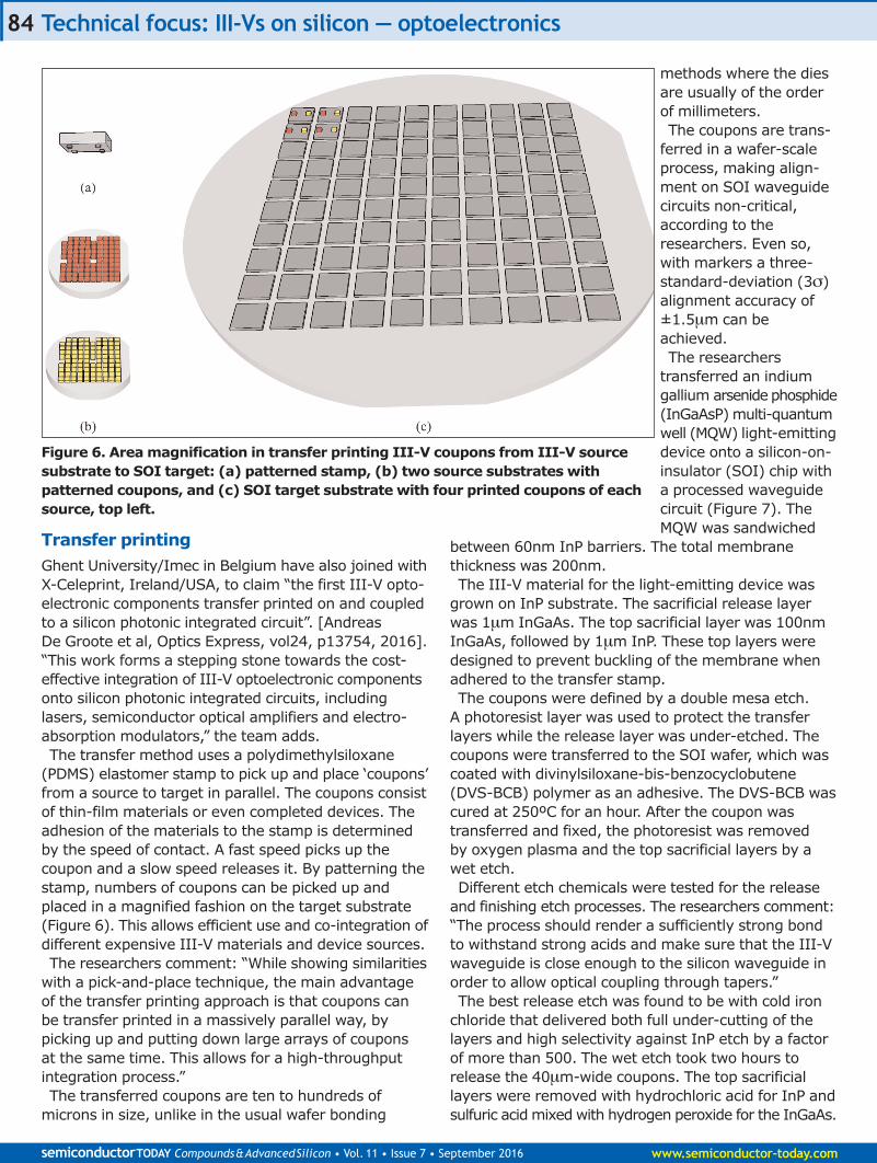
(PDMS) elastomer stamp to pick up and place ‘coupons’from a source to target in parallel. The coupons consistof thin-film materials or even completed devices. Theadhesion of the materials to the stamp is determinedby the speed of contact. A fast speed picks up thecoupon and a slow speed releases it. By patterning thestamp, numbers of coupons can be picked up andplaced in a magnified fashion on the target substrate(Figure 6). This allows efficient use and co-integration ofdifferent expensive III-V materials and device sources. The researchers comment: “While showing similarities
with a pick-and-place technique, the main advantageof the transfer printing approach is that coupons canbe transfer printed in a massively parallel way, by picking up and putting down large arrays of coupons at the same time. This allows for a high-throughputintegration process.”The transferred coupons are ten to hundreds of
microns in size, unlike in the usual wafer bonding
methods where the diesare usually of the orderof millimeters.The coupons are trans-
ferred in a wafer-scaleprocess, making align-ment on SOI waveguidecircuits non-critical,according to theresearchers. Even so,with markers a three-standard-deviation (3σ)alignment accuracy of±1.5μm can beachieved.The researchers
transferred an indiumgallium arsenide phosphide(InGaAsP) multi-quantumwell (MQW) light-emittingdevice onto a silicon-on-insulator (SOI) chip witha processed waveguidecircuit (Figure 7). TheMQW was sandwiched
between 60nm InP barriers. The total membrane thickness was 200nm.The III-V material for the light-emitting device was
grown on InP substrate. The sacrificial release layerwas 1μm InGaAs. The top sacrificial layer was 100nmInGaAs, followed by 1μm InP. These top layers weredesigned to prevent buckling of the membrane whenadhered to the transfer stamp.The coupons were defined by a double mesa etch.
A photoresist layer was used to protect the transferlayers while the release layer was under-etched. Thecoupons were transferred to the SOI wafer, which wascoated with divinylsiloxane-bis-benzocyclobutene(DVS-BCB) polymer as an adhesive. The DVS-BCB wascured at 250ºC for an hour. After the coupon wastransferred and fixed, the photoresist was removed by oxygen plasma and the top sacrificial layers by awet etch.Different etch chemicals were tested for the release
and finishing etch processes. The researchers comment:“The process should render a sufficiently strong bondto withstand strong acids and make sure that the III-Vwaveguide is close enough to the silicon waveguide inorder to allow optical coupling through tapers.”The best release etch was found to be with cold iron
chloride that delivered both full under-cutting of thelayers and high selectivity against InP etch by a factorof more than 500. The wet etch took two hours torelease the 40μm-wide coupons. The top sacrificial layers were removed with hydrochloric acid for InP andsulfuric acid mixed with hydrogen peroxide for the InGaAs.
Technical focus: III-Vs on silicon — optoelectronics
semiconductorTODAY Compounds&AdvancedSilicon • Vol. 11 • Issue 7 • September 2016 www.semiconductor-today.com
84
Figure 6. Area magnification in transfer printing III-V coupons from III-V sourcesubstrate to SOI target: (a) patterned stamp, (b) two source substrates withpatterned coupons, and (c) SOI target substrate with four printed coupons of eachsource, top left.

The proof-of-principle setup consisted of a single-spatial-mode broadband light-emitting device integratedwith SOI waveguides processed on 200mm wafers atImec’s CMOS pilot line. In this case, the III-V devicewas pumped with optical power from a 1310nm laserdirected through the SOI waveguide system. Measurements on the integrated III-V/SOI waveguide
structure indicate a power efficiency of the emitted lightat around 1550nm wavelength at the same order of
magnitude as achieved with traditional III-V-on-siliconbonding. “The 3dB bandwidth of 130nm is large, andcomparable as well to previously reported results,” the team writes. ■
The author Mike Cooke is a freelance technology journalistwho has worked in the semiconductor and advancedtechnology sectors since 1997.
Technical focus: III-Vs on silicon — optoelectronics
www.semiconductor-today.com semiconductorTODAY Compounds&AdvancedSilicon • Vol. 11 • Issue 7 • September 2016
85
Figure 7. Process flow of transfer printed, optically pumped light-emitting device: (a) InP starting layer stack,(b) coupon patterning, (c) encapsulation and tether definition, (d) top view after encapsulation and tetherdefinition. Further processing includes: (e) release etch, (f) pick-up of III-V coupon from source, (g) printing ofcoupon to SOI target, (h) removal of encapsulation and of sacrificial layers, (i) definition of light-emitting device.