a comparative study of c z-s m inverter … · in this paper, the conventional multilevel inverter...
TRANSCRIPT
Electrical and Electronics Engineering: An International Journal (ELELIJ) Vol 4, No 2, May 2015
DOI : 10.14810/elelij.2015.4212 143
A COMPARATIVE STUDY OF CONVENTIONAL AND
QUASI Z-SOURCE MULTILEVEL INVERTER FOR
PHOTOVOLTAIC APPLICATIONS
D.Umarani1 and Dr.R.Seyezhai
2
1Assistant Professor, Department of EEE, SSN College of Engineering, Chennai.
2Associate Professor, Department of EEE, SSN College of Engineering, Chennai.
ABSTRACT
In this paper, the conventional multilevel inverter (MLI) and Quasi Z-source multilevel inverter are
compared for their suitability to Photovoltaic (PV) applications. Five-level cascaded H-bridge
configuration has been considered for both the above mentioned inverter topologies. Simulation has been
carried for the PV source in Matlab/Simulink and interfaced with the above mentioned multilevel inverter
topologies. For the conventional MLI, an additional boost converter stage has been designed and
simulated. Impedance network has been designed for the Quasi Z-Source multilevel inverter. The
performance of the Quasi Z-Source multilevel inverter has been investigated based on its voltage boost
capability with the use of a single converter stage. Also, the additional converter stage required for the
conventional MLI for boost operation has been discussed. The suitability of the inverter topology for PV
application is analysed by computing the voltage gain, number of converter stages and output power. The
results are verified.
KEYWORDS
Multilevel inverter, Photovoltaic, Quasi Z-Source inverter, voltage boost, shoot through.
1.INTRODUCTION
The depletion of available non-renewable energy sources for the production of electricity may
lead to scarcity in the near future. Before it is completely vanished, we ought to find out a
solution that can replace the non-renewable energy source for production of electricity. The better
solution will be the use of renewable energy sources such as wind, solar etc., Solar energy based
electricity generation is clean and environment friendly. There are several researches going on to
efficiently trap the solar energy for generation of electricity. The electricity generated by the solar
panel will be a DC quantity. It should be converted to AC for feeding the power grid. So, the
inverter plays an important role in the energy conversion. In this paper a five-level cascaded H-
bridge configuration of the inverter has been considered. The conventional multilevel inverter
(MLI) consists of H-bridges connected in a cascaded way so that the total harmonic distortion of
the output may be reduced [8]-[9]. But it has several limitations. In order to overcome the
drawbacks, a new topology Quasi Impedance source multilevel inverter has been proposed for PV
applications. It has boost capability and voltage inversion in a single stage. Several modulation
strategies are available for generation of shoot through states. For the proposed Quasi Z-source
multilevel inverter (QZMLI), simple boost control technique is used. The shoot through is added
to the pulse width modulation so as to achieve voltage boost [1]-[3]. For the conventional MLI,
an additional boost converter stage is required for the same voltage boost as that of the QZMLI.
This boost converter is connected to the output of the solar source and then fed to the bridges of
Electrical and Electronics Engineering: An International Journal (ELELIJ) Vol 4, No 2, May 2015
144
the MLI. The simulation has been carried out using Matlab/Simulink platform and the simulation
results are discussed. Section- II explains the mathematical modeling of PV, section-III provides
the design specifications of boost converter employed in conventional MLI, section-IV discusses
the simulation results for the conventional five-level inverter. The proposed quasi Z-source MLI
is discussed in section -V followed by conclusion.
2. MATHEMATICAL MODELING OF PV
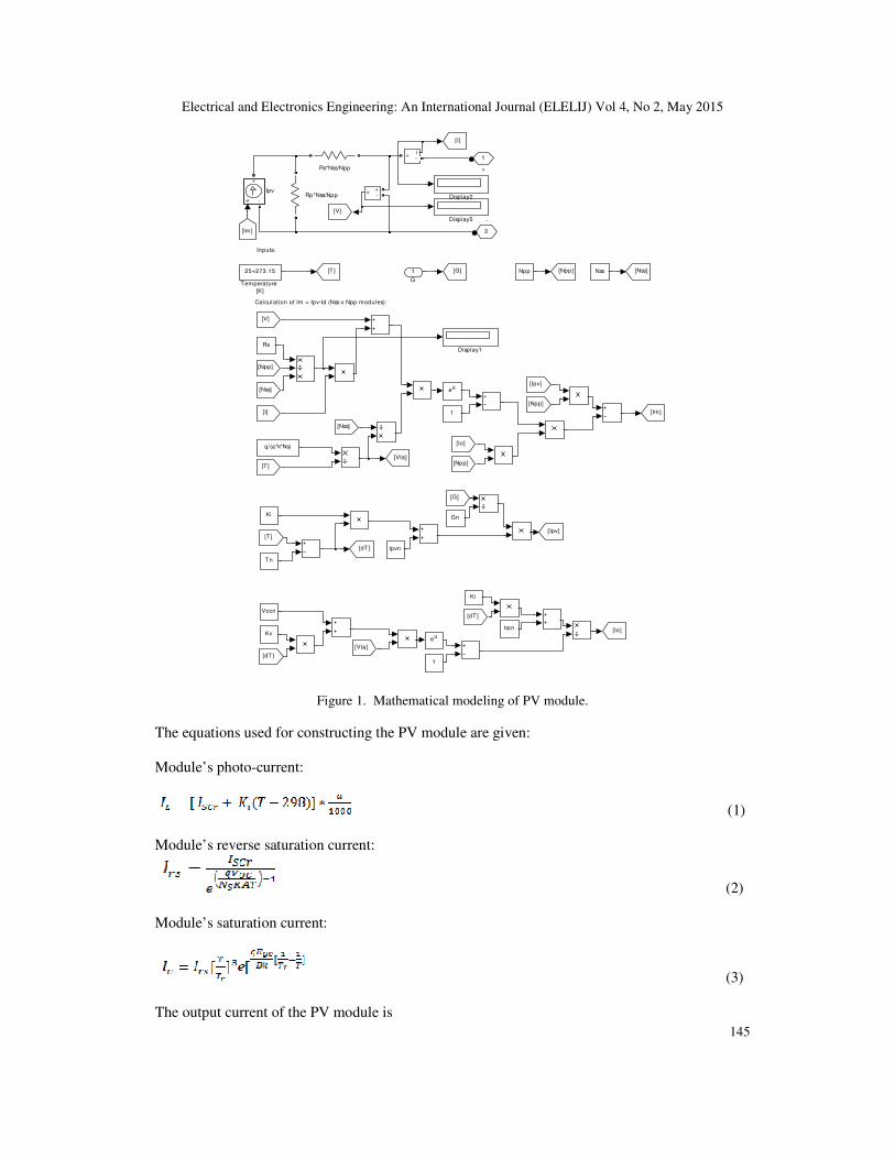
The PV module has been modeled using mathematical equations is shown in fig.1.The simulation
parameters are given in Table 1.
Table 1.PV Simulation Parameters
PV Parameters Rating
Open circuit voltage Voc 21.24 V
Short circuit current I sc 2.55 A
No of cells Ns 36
Insolation G 1000 W/m2
Ideality factor A 1.5
Operating temperature T 298 K
Electrical and Electronics Engineering: An International Journal (ELELIJ) Vol 4, No 2, May 2015
145
Calculation of Im = Ipv-Id (Nss x Npp modules):
Inputs:
2
-
1
+
v+-
25+273.15
Temperature
[K]
Rs*Nss/Npp
Rp*Nss/Npp
eu
eu
s -+
Ipv
i+
-
Display5
Display2
Display1Rs
Ki
1
q/(a*k*Ns)
Iscn
Nss
1
Kv
Vocn
Ki
Ipvn
Gn
Tn
Npp
[T]
[I]
[Im]
[V]
[Nss]
[Npp]
[Nss]
[Ipv]
[Io]
[Npp]
[dT]
[Vta]
[dT]
[G]
[T]
[Npp]
[Nss][Npp]
[Vta]
[dT]
[Ipv]
[Io]
[Im]
[G][T]
[V]
[I]
1
G
Figure 1. Mathematical modeling of PV module.
The equations used for constructing the PV module are given:
Module’s photo-current:
(1)
Module’s reverse saturation current:
(2)
Module’s saturation current:
(3)
The output current of the PV module is
Electrical and Electronics Engineering: An International Journal (ELELIJ) Vol 4, No 2, May 2015
146
(4)
Where V = VOC, NP = 1 and NS = 36, I is the PV array output current, V is the PV array output
voltage, Ns is the number of cells in series, Np is the number of cells in parallel, q is the charge of
an electron, k is the Boltzmann’s constant, A is the p-n junction ideality factor, T is the cell
temperature in Kelvin, Irs is the cell reverse saturation current [13].
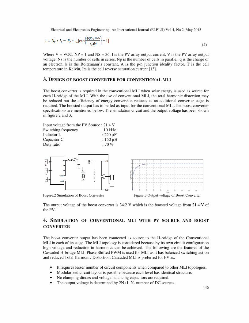
3. DESIGN OF BOOST CONVERTER FOR CONVENTIONAL MLI
The boost converter is required in the conventional MLI when solar energy is used as source for
each H-bridge of the MLI. With the use of conventional MLI, the total harmonic distortion may
be reduced but the efficiency of energy conversion reduces as an additional converter stage is
required. The boosted output has to be fed as input for the conventional MLI.The boost converter
specifications are mentioned below. The simulation circuit and the output voltage has been shown
in figure 2 and 3.
Input voltage from the PV Source : 21.4 V
Switching frequency : 10 kHz
Inductor L : 220 µF
Capacitor C : 150 µH
Duty ratio : 70 %
0 0.1 0.2 0.3 0.4 0.5 0.6 0.7 0.8 0.9 10
5
10
15
20
25
30
35
40
Time(s)
Ou
tpu
t V
olt
ag
e (
V)
Figure.2 Simulation of Boost Converter Figure.3 Output voltage of Boost Converter
The output voltage of the boost converter is 34.2 V which is the boosted voltage from 21.4 V of
the PV.
4. SIMULATION OF CONVENTIONAL MLI WITH PV SOURCE AND BOOST
CONVERTER
The boost converter output has been connected as source to the H-bridge of the Conventional
MLI in each of its stage. The MLI topology is considered because by its own circuit configuration
high voltage and reduction in harmonics can be achieved. The following are the features of the
Cascaded H-bridge MLI. Phase Shifted PWM is used for MLI as it has balanced switching action
and reduced Total Harmonic Distortion. Cascaded MLI is preferred for PV as:
• It requires lesser number of circuit components when compared to other MLI topologies.
• Modularized circuit layout is possible because each level has identical structure.
• No clamping diodes and voltage balancing capacitors are required.
• The output voltage is determined by 2N+1, N- number of DC sources.
Electrical and Electronics Engineering: An International Journal (ELELIJ) Vol 4, No 2, May 2015
147
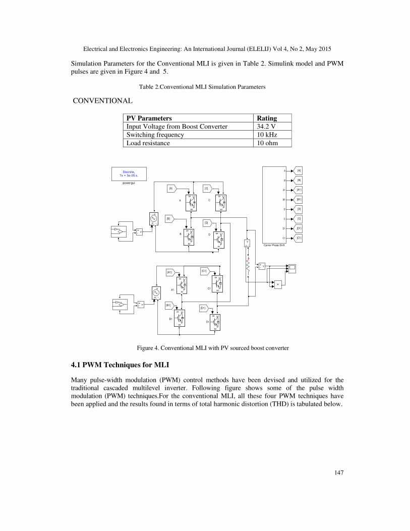
Simulation Parameters for the Conventional MLI is given in Table 2. Simulink model and PWM
pulses are given in Figure 4 and 5.
Table 2.Conventional MLI Simulation Parameters
CONVENTIONAL
PV Parameters Rating
Input Voltage from Boost Converter 34.2 V
Switching frequency 10 kHz
Load resistance 10 ohm
A1
B1
C1
D1
A
B
C
D
Discrete,Ts = 5e-05 s.
powergui
v+-
v+-
v+-
+
[C1]
[D1]
[C]
[D]
[B1]
[A1]
[B]
[A]
[C1]
[D1][B1]
[A1]
[B]
[D]
[C][A]
g CE
g CE
i+
-
s -+
s -+
A
B
A1
B1
D
C
D1
C1
Carrier Phase Shift
g CE
g CE
g CE
g CE
g CE
g CE
Figure 4. Conventional MLI with PV sourced boost converter
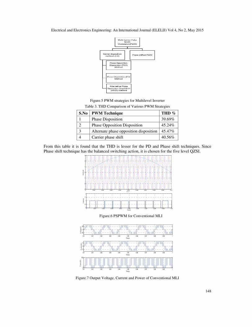
4.1 PWM Techniques for MLI
Many pulse-width modulation (PWM) control methods have been devised and utilized for the
traditional cascaded multilevel inverter. Following figure shows some of the pulse width
modulation (PWM) techniques.For the conventional MLI, all these four PWM techniques have
been applied and the results found in terms of total harmonic distortion (THD) is tabulated below.
Electrical and Electronics Engineering: An International Journal (ELELIJ) Vol 4, No 2, May 2015
148
Figure.5 PWM strategies for Multilevel Inverter
Table 3. THD Comparison of Various PWM Strategies
S.No PWM Technique THD %
1 Phase Disposition 39.69%
2 Phase Opposition Disposition 45.24%
3 Alternate phase opposition disposition 45.47%
4 Carrier phase shift 40.56%
From this table it is found that the THD is lesser for the PD and Phase shift techniques. Since
Phase shift technique has the balanced switching action, it is chosen for the five level QZSI.
0 0.001 0.002 0.003 0.004 0.005 0.006 0.007 0.008 0.009 0.01-3
-2
-1
0
1
2
3
Time(s)
Am
plit
ud
e
0 0.001 0.002 0.003 0.004 0.005 0.006 0.007 0.008 0.009 0.010
0.5
1
1.5
2
Time(S)
Am
plit
ud
e
Figure.6 PSPWM for Conventional MLI
Figure.7 Output Voltage, Current and Power of Conventional MLI
0.9 0.91 0.92 0.93 0.94 0.95 0.96 0.97 0.98 0.99 1
-50
0
50
Time(s)
Vo
lta
ge
(V)
0.9 0.91 0.92 0.93 0.94 0.95 0.96 0.97 0.98 0.99 1
-5
0
5
Time(s)
Cu
rre
nt(
A)
0.9 0.91 0.92 0.93 0.94 0.95 0.96 0.97 0.98 0.99 10
500
Time(s)
Po
we
r(W
)
Electrical and Electronics Engineering: An International Journal (ELELIJ) Vol 4, No 2, May 2015
149
The cascaded output voltage of the conventional MLI having PV sourced boost converter is found
to be 68.4 V. The power consumed by the load is 468 W. It is shown in fig.7
5. QUASI Z-SOURCE MLI INTERFACED WITH PV
Conventional MLI has the following limitations:
• The ac output voltage is limited below the dc–rail voltage.
• If overdrive is needed then an additional converter stage is added to obtain the desired
output. It increases the system cost and efficiency.
• The upper and lower devices cannot be gated simultaneously as it results in short-circuit
with the source and deterioration of devices.
• Dead time is required for triggering both upper and lower devices which results in the
distortion of the waveform.
So we go for the Impedance type inverters which can overcome all the disadvantages of
conventional MLI. In addition to that these type of inverters can invert as well as boost the
voltage in a single stage. These features are value added to the Z-source inverters because of the
unique impedance or LC network present as the interface between PV source and the inverter
bridge. In this paper, we have discussed the Quasi type impedance inverter as it acquires all the
advantages of the Z-source inverter. Also this type of topology has reduced component ratings
and improved reliability. Shoot-through is added to the PWM pulses in order to achieve the
voltage boosting action. The inverter operates in the shoot-through mode during the shoot-
through period. It results in a wide voltage gain [7] - [11]. The impedance network design is
shown below.
Inductance:
(5)
Capacitance:
(6)
Where,
To - Shoot-through Interval, m - Modulation Index, Rc - Peak current ripple in %, Rv - Peak
voltage ripple in %, IL - Rated Load current, fs - Switching frequency.
Electrical and Electronics Engineering: An International Journal (ELELIJ) Vol 4, No 2, May 2015
150
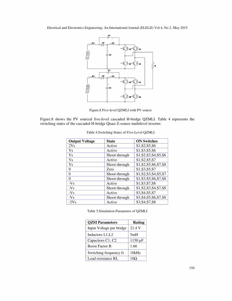
Figure.8 Five-level QZMLI with PV source
Figure.8 shows the PV sourced five-level cascaded H-bridge QZMLI. Table 4 represents the
switching states of the cascaded H-bridge Quasi Z-source multilevel inverter.
Table 4.Switching States of Five-Level QZMLI
Output Voltage State ON Switches
2Vs Active S1,S2,S5,S6
Vs Active S1,S3,S5,S6
Vs Shoot-through S1,S2,S3,S4,S5,S6
Vs Active S1,S2,S5,S7
Vs Shoot-through S1,S2,S5,S6,S7,S8
0 Zero S1,S3,S5,S7
0 Shoot-through S1,S2,S3,S4,S5,S7
0 Shoot-through S1,S3,S5,S6,S7,S8
-Vs Active S1,S3,S7,S8
-Vs Shoot-through S1,S2,S3,S4,S7,S8
-Vs Active S3,S4,S5,S7
-Vs Shoot-through S3,S4,S5,S6,S7,S8
-2Vs Active S3,S4,S7,S8
Table 5.Simulation Parameters of QZMLI
QZSI Parameters Rating
Input Voltage per bridge 21.4 V
Inductors L1,L2 5mH
Capacitors C1, C2 1150 µF
Boost Factor B 1.66
Switching frequency fs 10kHz
Load resistance RL 10Ω
Electrical and Electronics Engineering: An International Journal (ELELIJ) Vol 4, No 2, May 2015
151
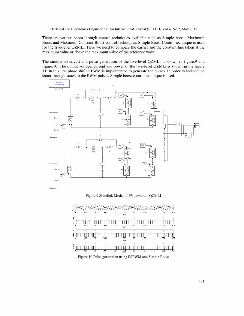
There are various shoot-through control techniques available such as Simple boost, Maximum
Boost and Maximum Constant Boost control techniques. Simple Boost Control technique is used
for the five-level QZMLI. Here we need to compare the carrier and the constant line taken at the
maximum value or above the maximum value of the reference wave.
The simulation circuit and pulse generation of the five-level QZMLI is shown in figure.9 and
figure.10. The output voltage, current and power of the five-level QZMLI is shown in the figure
11. In this, the phase shifted PWM is implemented to generate the pulses. In order to include the
shoot-through states to the PWM pulses, Simple boost control technique is used.
A1
B1
C1
D1
A
B
C
D
C1
C2
C3
C4
Discrete,Ts = 5e-05 s.
powergui
v+-
v+-
v+-
Conn1
Conn2
Subsystem1
Conn1
Conn2
Subsystem
+
+
++
+
+
L4
+
L3
+
L2
+
L1
[C1]
[D1]
[B1]
[A1]
[B][D]
[C][A]
g CE
D4
D3
g CE
i+
-
s -+
s -+
g CE
g CE
g CE
g CE
g CE
g CE
Figure.9 Simulink Model of PV powered QZMLI
Figure.10 Pulse generation using PSPWM and Simple Boost
Electrical and Electronics Engineering: An International Journal (ELELIJ) Vol 4, No 2, May 2015
152
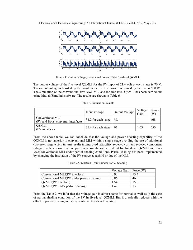
Figure.11 Output voltage, current and power of the five-level QZMLI
The output voltage of the five-level QZMLI for the PV input of 21.4 volt at each stage is 70 V.
The output voltage is boosted by the boost factor 1.5. The power consumed by the load is 550 W.
The simulation of the conventional five-level MLI and the five-level QZMLI has been carried out
using Matlab/Simulink software. The results are shown in Table 6.
Table 6. Simulation Results
Input Voltage Output Voltage
Voltage
Gain
Power
(W)
Conventional MLI
(PV and Boost converter interface) 34.2 for each stage 68.4 1 468
QZMLI
(PV interface) 21.4 for each stage 70 1.63 550
From the above table, we can conclude that the voltage and power boosting capability of the
QZMLI is far superior to conventional MLI within a single stage avoiding the use of additional
converter stage which in turn results in improved reliability, reduced cost and reduced component
ratings. Table 7 shows the comparison of simulation carried out for five-level QZMLI and five-
level conventional MLI under partial shading conditions. Partial shading has been implemented
by changing the insolation of the PV source at each H-bridge of the MLI.
Table 7.Simulation Results under Partial Shading
Voltage Gain Power(W)
Conventional MLI(PV interface) 0.93 53.3
Conventional MLI(PV under partial shading) 0.86 46
QZMLI(PV interface) 1.54 150
QZMLI(PV under partial shading) 1.47 130
From the Table 7, we infer that the voltage gain is almost same for normal as well as in the case
of partial shading condition of the PV in five-level QZMLI. But it drastically reduces with the
effect of partial shading in the conventional five-level inverter.
Electrical and Electronics Engineering: An International Journal (ELELIJ) Vol 4, No 2, May 2015
153
6. CONCLUSIONS
The simulation has been performed for the five-level cascaded H-bridge conventional inverter
with PV as the source at each H-bridge. For this, PV was modeled using mathematical modeling
in Matlab/Simulink. A boost converter was designed with duty ratio 70% for a switching
frequency of 10 kHz to achieve voltage boost in the output of the inverter. The output of the five-
level conventional MLI was obtained as 68.4 V for an input of 34.2 V at each stage of PV
interfaced with boost converter. The voltage gain achieved is 1. But the simulation model of five-
level cascaded H-bridge Quasi Z-source inverter connected to the same PV source without any
boost converter provided an output voltage of 70 V in a single stage with a voltage gain of 1.63.
Thus it indicates we can cut down the cost and improve the efficiency of the inverter. The L and
C components also have reduced ratings in the case of QZSI. The power of the five-level QZMLI
is 550 W which is greater when compared to the 468 W of the conventional five-level MLI. Also,
under the partial shading conditions of the PV module, the boost converter cannot provide a
stable voltage to the H-bridges of the conventional MLI. So the output voltage will reduce
drastically and it is clearly shown in the simulation results under partial shading. But because of
the presence of the impedance network between the PV source and the inverter bridge, the
QZMLI has continuous current characteristic. This will not aid in reducing the output voltage
because of its operation in shoot-through state. Thus, we can conclude that QZMLI can be
efficiently used for photovoltaic applications.
ACKNOWLEDGEMENTS
The authors would like to thank the All India Council for Technical Education (AICTE) for
funding and supporting this project.
REFERENCES
[1] Baoming Ge ; Abu-Rub, H. ; Fang Zheng Peng ; Qin Lei ; de Almeida, A.T. ; Ferreira, F.J.T.E. ;
Dongsen Sun ; Yushan Liu "An Energy Stored Quasi-Z-Source Inverter for Application to
Photovoltaic Power System." IEEE Transactions on Industrial Electronics, Volume 60 , Issue: 10 ,
Oct. 2013:4468 - 4481.
[2] Dongsen Sun, Baoming Ge, Fang Zheng Peng, Haitham, A.R., Daqiang Bi ,Yushan Liu "A new grid-
connected PV system based on cascaded H-bridge quasi-Z source inverter.", IEEE International
Symposium on Industrial Electronics (ISIE), 2012.
[3] S. Thangaprakash, A. Krishnan. “Comparative evaluation of modified pulse width modulation
schemes of Z-source inverter for various applications and demands”. International Journal of
Engineering, Science and Technology , Volume. 2, No. 1, 2010, pp. 103-115
[4] F.Z. Hamidon,P.D. Abd. Aziz,N.H. Mohd Yunus“Photovoltaic Array Modelling with P&O MPPT
Algorithm in MATLAB ”), IEEE International Conference on Statistics in Science, Business, and
Engineering (ICSSBE), 2012.
[5] J. Anderson and F. Z. Peng, "Four quasi-Z-Source inverters," PESC '08 - 39th IEEE Annual Power
Electronics Specialists Conference, June 15, 2008 - June 19, 2008, Rhodes, Greece, 2008, pp. 2743-
2749.
[6] Peng, Fang Zheng. "Z-source inverter. " , IEEE Transactions on Industry Applications , Volume 39.2
(2003),pp.504-510.
[7] Y. Li, J. Anderson, F.Z. Peng, and D.C. Liu, “Quasi-Z-source inverter for photovoltaic power
generation systems,” IEEE Twenty-Fourth Annual Applied Power Electronics Conference and
Exposition, APEC 2009, Washington DC, USA, pp. 918-924, 15-19 Feb. 2009.
[8] J. Rodriguez, J.-S. Lai, and F. Z. Peng, “Multilevel inverters: A survey of topologies, controls, and
applications,” IEEE Transactions on Industrial Electronics, volume 49.4, pp. 724–738, Aug. 2002.
[9] B. P. McGrath and D. G. Holmes, “Multicarrier PWM strategies for multilevel inverters,” IEEE
Transactions on Industrial Electronics, volume 49, no. 4, pp. 858– 867, Aug. 2002.
Electrical and Electronics Engineering: An International Journal (ELELIJ) Vol 4, No 2, May 2015
154
[10] M.Calais, L. J. Borle and V.G. Agelidis, “Analysis of Multicarrier PWM Methods for a Single-phase
Five Level Inverter”, IEEE Power Electronics Specialist Conference, PESC’01,July 2001,pp 1351-
1356.
Authors
D.Umarani received her B.E degree (Electrical and Electronics) in the year 2011 from
Mepco Schlenk Engineering College, Sivakasi and M.E in Power Electronics and Drives
from SSN College of Engineering in 2014. Currently she an assistant professor at SSN
College of Engineering, Chennai. Her areas of interest are Z-Source and Quasi Z-Source
inverters.
Dr.R.Seyezhai obtained her B.E. (Electronics & communication Engineering) from Noorul
Islam College of Engineering, Nagercoil in 1996 and her M.E in Power Electronics & Drives
from Shanmugha College of Engineering, Thanjavur in 1998 and Ph.D from Anna
University, Chennai, in 2010 . She has been working in the teaching field for about 15 Years.
She has published 120 papers in the area of Power Electronics & Drives. Her areas of interest
include SiC Power Devices & Multilevel Inverters.