a fully 3d-printed integrated electro-chemical sensor...
TRANSCRIPT

A Fully 3D-printed Integrated
Electro-chemical Sensor System
by
Yue Dong
B.Sc., Simon Fraser University, 2015
Thesis Submitted in Partial Fulfillment of the
Requirements for the Degree of
Master of Applied Science
in the
School of Mechatronic Systems Engineering
Faculty of Applied Science
© Yue Dong
SIMON FRASER UNIVERSITY
Summer 2017
Copyright in this work rests with the author. Please ensure that any reproduction or re-use is done in accordance with the relevant national copyright legislation.

ii
Approval
Name: Yue Dong
Degree: Master of Applied Science
Title: A Fully 3D-printed Integrated Electro-chemical Sensor System
Examining Committee: Chair: Dr. Siamak Arzanpour, P. Eng Associate Professor
Dr. Woo Soo Kim, P. Eng Senior Supervisor Associate Professor
Dr. Jiacheng (Jason) Wang Supervisor Assistant Professor
Dr. Ash M. Parameswaran, P. Eng Internal Examiner Professor School of Engineering Science
Date Defended/Approved:
30 August 2017

iii
Abstract
This thesis investigates the design, fabrication and characterization of a 3D printed
electro-chemical sensor as well as compact potentiostat circuit on Printed Circuit Board
(PCB) for portable electro-chemical sensing applications. Conductive 3D printing
technologies are investigated as well as the advances in sensors and electronics
applications. An optimized Directly Ink Writing (DIW) technique is adapted in a novel 3D-
PCB fabrication platform using silver nanoparticle ink for electronics applications. An
electrochemical device called potentiostat is designed based on an open source system.
Its prototype is 3D printed on FR4 substrate. Using the same 3D platform, a lactate sensor
which is comprised of 3-electrodes is printed on the flexible substrate. Together, the 3D
printed system demonstrates the electrochemistry test including cyclic voltammetry (CV)
and amperometry. Results of this research demonstrate that 3D-PCB technology can
significantly accelerate the fabrication process of conventional electronics, and merge its
capability into electrochemical applications.
Keywords: 3D printing; electrochemical devices; biosensors; 3D printed circuits;
flexible printed circuits

iv
I would like to dedicate this thesis to my loving family

v
Acknowledgements
I wish to thank my advisor, Dr. Woo Soo Kim, for his support on this project, as well as the
other members of my thesis committee.
To the staff of the SFU MSE department, a heartfelt thank you for all of your hard work
keeping the program operating.
Finally, it has been an honor working with all of the other members of the stretchable
devices laboratory, and our many conversations, on topic or off, were always a pleasure.

vi
Table of Contents
Approval .......................................................................................................................... ii
Abstract .......................................................................................................................... iii
Acknowledgements ......................................................................................................... v
Table of Contents ........................................................................................................... vi
List of Tables ................................................................................................................. viii
List of Figures................................................................................................................. ix
List of Acronyms ............................................................................................................ xiii
Chapter 1. Introduction .............................................................................................. 1
1.1. Motivation .............................................................................................................. 2
1.2. Objectives.............................................................................................................. 6
1.3. Contribution ........................................................................................................... 6
1.4. Thesis Organization ............................................................................................... 7
Chapter 2. Electrochemistry and 3D Electronics Printing ....................................... 8
2.1. Electrochemistry and its Application ...................................................................... 8
2.1.1. Electrochemical Cell .................................................................................... 12
Working Electrode .................................................................................................. 12
Reference Electrode .............................................................................................. 12
Counter Electrode .................................................................................................. 14
2.1.2. Potentiostat ................................................................................................. 14
2.1.3. Method of Analysis ...................................................................................... 15
2.1.4. Biosensor and Principle of Lactate Sensing ................................................. 21
2.2. 3D Printing Technologies for Sensors and Electronics......................................... 23
2.2.1. Current 3D Printing Technology ................................................................... 23
2.2.1.1 Fused Deposition Modeling (FDM) ............................................................. 24
2.2.1.2Direct Ink Writing (DIW) ............................................................................... 25
2.2.1.3. Photocuring (SLA, DLP) ............................................................................ 26
2.2.1.4. Lamination (LOM) ...................................................................................... 28
2.2.1.5. Selective Laser Sintering and Selective Laser Melting (SLS, SLM) ........... 29
2.2.1.6. Photopolymer Jetting (Ployjet) ................................................................... 30
2.2.2. 3D Biosensor Applications ........................................................................... 32
2.2.3. 3D Electronics Applications ......................................................................... 33
2.2.4. Conductive Nano-Material Printing .............................................................. 36
Chapter 3. Development of 3D Printed Electrochemical System .......................... 38
3.1. 3D Printing of Conductive Ink .............................................................................. 38
3.2. Building Processes for PCB Printing .................................................................... 40
3.2.1. Pre-calibration ............................................................................................. 41
3.2.2. Top Layer Circuit Printing ............................................................................ 42
3.2.3. Drilling ......................................................................................................... 42
3.2.4. Bottom Layer Circuit Printing ....................................................................... 43

vii
3.2.5. Filling ........................................................................................................... 44
3.2.6. Solder Paste Printing ................................................................................... 45
3.2.7. Reflow ......................................................................................................... 46
3.3. Parameter Control for PCB Printing ..................................................................... 47
3.4. 3D Printed Flexible Electro-chemical Sensor ....................................................... 52
3.4.1. Formation of Working Electrode .................................................................. 53
3.4.2. Generation of Reference Electrode .............................................................. 54
3.5. Design of 3D Printed Potentiostat ........................................................................ 55
3.5.1. Design and Fabrication of Potentiostat Circuits ............................................ 56
3.5.2. Development of Potentiostat Firmware ........................................................ 61
3.6. 3D Printed Potentiostat on Epoxy Board .............................................................. 62
3.6.1. Design Optimization of Potentiostat PCB ..................................................... 62
3.6.2. Prototyping of 3D Printed Potentiostat ......................................................... 63
Chapter 4. Characterization of 3D Printed Electrochemical System .................... 65
4.1. Characterization of 3D printed Lactate Sensor .................................................... 65
4.2. Cyclic Voltammetry for Redox Analysis ............................................................... 66
4.3. Amperometric i-t curve and Calibration ................................................................ 69
Chapter 5. Conclusion and Future Work ................................................................ 71
5.1. Conclusion........................................................................................................... 71
5.2. Future Works ....................................................................................................... 72
References ................................................................................................................... 73
Appendix A. Early electrodes design setup ......................................................... 82
Appendix B. Programming Setup ......................................................................... 83
Appendix C. Potentiostat Circuit Design Detail ................................................... 84
Appendix D. Microcontroller code ........................................................................ 86

viii
List of Tables
Table 2.1. Summary of each printing methods ........................................................ 31
Table 2.2. Summary of 3D-printed sensors ............................................................. 32

ix
List of Figures
Figure 1.1 Fabrication comparison between conventional PCB (left) and 3D PCB (right) ....................................................................................................... 3
Figure 2.1. A voltaic cell transforms the energy released by a spontaneous redox reaction into electrical energy [24]. Licensed under by CC 3.0. ................ 9
Figure 2.2. An electrolytic cell, an external electrical source is used to generate a potential difference between the electrodes that forces electrons to flow, driving a nonspontaneous redox reaction[24]. Licensed under by CC 3.0. ............................................................................................................... 10
Figure 2.3. Schematic of an Ag/AgCl reference electrode [27]. Licensed under by CC 3.0. ......................................................................................................... 13
Figure 2.4. Schematic diagram of a general potentiostat and connection with an electrochemical cell ................................................................................ 15
Figure 2.5 Summary of interfacial electrochemical techniques. The specific techniques are shown in red, the experimental conditions are shown in blue, and the analytical signals are shown in green [24]. By LibreTexts is licensed under CC 3.0. ........................................................................... 16
Figure 2.6. Close look of reaction at surface of electrode, both chemical transfer and mass transfer are involved [29]. Reprinted with permission. ................... 18
Figure 2.2.7. Typical potential sweep execution signal (A) and an ideal CV curve (B) [24]. By LibreTexts is licensed under CC 3.0. ......................................... 19
Figure 2.8. Cyclic voltammograms for R obtained at (A) a faster scan rate and (B) a slower scan rate [24]. By LibreTexts is licensed under CC 3.0. .............. 20
Figure 2.9. Illustration of the immobilized enzyme [29]. Reprinted with permission. . 21
Figure 2.10. 3D-printing process. A digital model of the object is obtained through CAD software or 3D scanner. The 3D model design is then converted to the STL format to G-code file. Finally, the printer starts depositing the material following the layer-by-layer sequence [51]. Reprinted with permission. ............................................................................................. 23
Figure 2.11. Schematic diagram of fused deposition modeling (FDM). A nozzle fed with a thermoplastic wire is moved in three dimensions across the building platform onto which molten voxels of a polymer are applied [51]. Reprinted with permission. ..................................................................... 24
Figure 2.12. Schematic diagram of direct ink writing. A material dispenser connected to a computer-controlled robot, scans across the building platform, depositing the ink material in a layer-by-layer manner[51]. Reprinted with permission. ............................................................................................. 25
Figure 2.13. (A) Stereolithography (SLA) in a bath configuration where a laser beam is scanned across the liquid surface to polymerize the resin. Successive layers are created by lowering the movable table, allowing the fresh liquid resin to be exposed. (B) DLP in a layer configuration in which a laser beam is scanned from the bottom of the liquid tank through a transparent window. The polymerized layer attaches to the table, which is then moved upwards to refill the gap between the first layer and the window with fresh resin[51]. Reprinted with permission. ...................................................... 26

x
Figure 2.14. Schematic diagram of laminated object manufacturing (LOM). The first sheet of material is loaded onto the building platform. A PC-controlled cutting system consisting of a laser beam (or a mechanical blade) is then used to define the layer contour. Once the excess material is removed, a new sheet is loaded with a laminating roller which ensures good adhesion of the layers [51]. Reprinted with permission. ......................................... 28
Figure 2.15. Schematic diagram of Selective Laser Sintering and Selective Laser Melting (SLS, SLM) [51]. Reprinted with permission. .............................. 29
Figure 2.16. Schematic diagram of Photopolymer jetting (Ployjet) [51]. Reprinted with permission. ............................................................................................. 30
Figure 2.17. 3D printed electronics (a)magnetic flux sensor system with curved surfaces and modern miniaturized electronic components[98] (b)CubeSat 3D-printed module produced by using stereolithography and direct print technologies[98] (c) 3D-printed CubeSat module produced by using fused deposition modeling [98]. Reprinted with permission. ............................. 35
Figure 2.18. Electrical resistivity properties of conductive materials [101-107] ........... 37
Figure 3.1. Voltera V-ONE Direct Ink Printer ............................................................ 38
Figure 3.2. Direct ink writing mechanism detail ....................................................... 39
Figure 3.3. Voltera Software Slicing Feature of SMD circuit pattern (left) SMD QFN28 footprint (middle) sliced STI file with 0.15 line space (right) 0.1 line space. ............................................................................................................... 39
Figure 3.4. Flow chart of the additive manufacturing of- of 3D printed PCB .............. 40
Figure 3.5. Calibration procedures for substrate height profile ................................. 41
Figure 3.6. Ink level calibration procedure before printing ........................................ 41
Figure 3.7. Top layer circuit printing procedure ........................................................ 42
Figure 3.8. Circuit patterns of through-hole, vias, and pads for printing .................... 43
Figure 3.9. (left) Dermer Mode 3000 press driller (middle) PCB drill bits set (right) image of drilling process for through-hole and vias ................................. 43
Figure 3.10. Illustration of cross section of PCB with vias and through-hole .............. 44
Figure 3.11. (a) Printed circuit pattern with vias on top layer after drilling (b) vias on bottom layer after drilling ........................................................................ 44
Figure 3.12. Image of filled vias, unfilled vias, and open through-holes on 3D-PCB ... 45
Figure 3.13. Image of dispensed solder paste on printed circuit pads ........................ 45
Figure 3.14. Reflow profile used for 3D-PCB .............................................................. 46
Figure 3.15. Sliced PCB G-code using different line spacing value ............................ 47
Figure 3.16. Printing quality comparison (a) large uncoverd area when line space is too high (b) bad dispense when nozzle position is too high or ink extrusion amount is too small (c) over pressed ink when nozzle position is too low or ink extrusion amount is too large ............................................ 48
Figure 3.17. Extruded ink pattern with optimized printing parameters ........................ 48
Figure 3.18. Electrical resistivity measurement by four point probe method [108]. Reprinted with permission. ..................................................................... 49
xi
Figure 3.19. Electrical resistivity measurement by two probe method [108]. Reprinted with permission. ..................................................................................... 50
Figure 3.20. (left) Printed ink specimen on PET substrate with different baking temperatures (right) resistivity measurement setup using the probe station ............................................................................................................... 50
Figure 3.21. Electrical resistivity of printed silver ink under different baking temperature ............................................................................................................... 51
Figure 3.22. Micro image of printed AgNP ink before baking and after baking using optimized baking temperature ................................................................ 51
Figure 3.23. First sensor design with card edge connection feature (left) CAD deisgn (middle) printed electrodes on rigid FR4 board (right) printed electrodes on PET substrate ................................................................................... 52
Figure 3.24. Final sensor design with card edge connection feature (left) CAD design (middle) printed electrodes on rigid FR4 board (right) printed electrodes on PET substrate ................................................................................... 53
Figure 3.25. Cross sectional structure of the working electrode with enzyme layer .... 54
Figure 3.26. (left) proposed printed lactate biosensor prototype with WE covered by the enzyme and chloridized RE (right) lactate biosensor connected with a 3-pin card edge connector ...................................................................... 55
Figure 3.27. Block diagram of the potentiostat ........................................................... 56
Figure 3.28. Detail schematic diagram of the proposed potentiostat system design ... 57
Figure 3.29. Electrometer generator circuit ................................................................ 58
Figure 3.30. OPA380 trans-impedance amplifier i-v converter ................................... 58
Figure 3.31. 2nd order Sallen-Key low pass filter circuit ............................................. 59
Figure 3.32. Schematic of potentiostat circuit design using Eagle PCB. Zoom in detail is in appendix C...................................................................................... 60
Figure 3.33. (left)Test potentiostat PCB fabricated by the conventional method (right) Test setup for the conventional potentiostat ........................................... 60
Figure 3.34. Early potentiostat prototype on separated 3D-PCBs .............................. 63
Figure 3.35. (a) latest PCB layout in EagleCAD (b) proposed connection feature between 3D-PCB potentiostat and sensor .............................................. 64
Figure 3.36. The final 3D-PCB p4otentiostat with SMD components and DIP sockets ............................................................................................................... 64
Figure 4.1. Lactate biosensor charetericaztion test results: (a) cyclic voltammetry curve using 5,10,and 15mM lactate solution. (b) Amperometric measurements in new condition and in 24 hours. ................................... 66
Figure 4.2. (left) cyclic voltammograms measurement of 15 mM Lactic Acid solution at different scan rates from 50mV/s to 400mV/s, (right) linear relation between absolute value of anodic current peak and square root of scan rate......................................................................................................... 67
Figure 4.3. Cyclic voltammetry measurements of lactic acid at 100mV/s scan rate via (a) proposed potentiostat design using conventional PCB fabrication method (b) proposed potentiostat design using 3D printing method ...... 68

xii
Figure 4.4. (a) test setup for 3D-PCB potentiostat prototype with lactate sensor (b) zoom in the image of drop cast of lactate acid solution on the sensor .... 69
Figure 4.5. Amperometric measurements within lactate solutions. (a) proposed potentiostat design using conventional PCB fabrication method (b) proposed potentiostat design using a 3D printing method ...................... 70

xiii
List of Acronyms
ABS Acrylonitrile Butadiene Styrene
ADC Analog To Digital Converter
AgNW Silver Nanowire
AgNP Silver Nanoparticle
AuNP Gold Nanoparticle
BSA Bovine Serum Albumin
CAD Computer-Aided Design
CE Counter Electrode
CV Cyclic Voltammetry
DAC Digital To Analog Converter
DIW Directly Ink Writing
FDM Fused Deposition Modeling
GA Glutaraldehyde
GUI Graphical User Interface
LOD Lactate Oxidase
LOM Laminated Object Manufacturing
PA Polyamide
PBS Phosphate Buffer Saline
PC Polycarbonate
PCB Printed Circuit Board
PDMS Polydimethylsiloxane
PET Polyethylene Terephthalate
PLA Polylactic Acid
PU Polyurethane
RE Reference Electrode
SLA Selective Laser Apparatus
SLS Selective Laser Sintering
SMD Surface Mounted Devices
STL Stereo Lithography
WE Working Electrode

1
Chapter 1. Introduction
The applications for 3D printing, also known as additive manufacturing (AM) are
exploding since 3D printing technology was first introduced in 1984 with the invention of
an innovative stereolithographic device by Charles Hull [1]. However, it was not until the
commercialization of 3D Systems’ stereolithography (STL) based 3D printer that
commercial 3D printers began to take off [2]. Following this, several other technologies for
AM were commercialized including Laminated Object Manufacturing (LOM) and Selective
Laser Sintering (SLS) in 1986, and Fused Deposition Modeling (FDM) and MIT’s inkjet
binder-based 3D printing in 1989 [2-3]. As new and more advanced technologies have
emerged, the possibility to produce end-use productions on AM systems has become a
reality, and the potential to create designs that are impossible to produce through other
means has emerged. The process of 3D-printing starts with the creation of a virtual model
of the object to be printed. This can be achieved by using computer-aided design (CAD)
software, a three-dimensional scanner, or using photogrammetry where the model is
obtained through the combination of several images of the object taken from different
positions. Once the 3D model is created, it needs to be converted to the STL file format
which stores the information of the model’s surfaces as a list of coordinates of triangulated
sections. This file format is universally recognized as it can be read by all 3D printer
software, which then converts the data to a G-code file after a slicing process. The slicing
procedure consists of the generation of several 2D cross section layers of the entire object.
Finally, the printer starts depositing the material following the successive sequencing of
such 2D layers, which are printed on top of the other, until the desired 3D object is created
[4].
3D-printing enables almost unlimited possibilities for rapid prototyping and even
massive manufacturing in some specific applications, such as fabricating thermofomring
unit. Therefore, it has been considered for applications in numerous research fields such
as mechanical engineering, medicine, and chemistry. Electrochemistry is one of the
potential applications that can certainly benefit from 3D-printing technologies, paving the
way for the design and rapid prototype of cheaper, higher performing, and ubiquitously

2
available electrochemical devices include sensor elements and backend electrochemical
measurement electronics. Electrochemistry is the branch of physical chemistry studies the
relationship between electricity, as a measurable and quantitative phenomenon, and
identifiable chemical change [5]. The modern electrochemical system consists of two
major parts: an electrochemical cell/sensor and an electrochemical signal acquisition
electronics. Developing such electronics system usually take months or even years of
time. Developers have to work from designing to prototyping back and forth in several
cycles; it is a very time-consuming process. Particularly during the prototyping stage, the
developer needs to send their design to off-site manufacturing service and the waiting
periods are quite long. Therefore, prototyping efficient can be significantly increased by
3D printing technology if it has capability to fabricating both the electronics device and
electrochemical sensors.
Usage of 3D printing for electronics device still remains largely unexplored, mainly
because the lack of capability to fabricate the printed circuit boards (PCBs). A PCB is used
primarily to create a connection between components, such as resistors, integrated
circuits (ICs), connectors [6]. Together they deliver the functionality in any electronics
today. Not surprisingly, the 3D printed electronics industry is in its early stage, more or
less at the same level of adoption as regular 3D prototyping was in 2009 [7-8]. The slow
adoption is not from a lack of interest or need; instead, it is because creating 3D printing
technology for PCBs is exceedingly complex and previously developed 3D printing method
did not solve these challenges. A suitable method and printer must be able to print
conductive traces, which is the domain of printed electronics and produce components
that meet the demanding performance requirements of consumer electronics, internet of
things and even wearables.
1.1. Motivation
According to the 3D PCB printer readiness survey which garnered responses from
nearly 300 electronics manufacturers and designers around the world [9]. 16% of
respondents said their companies spend more than $100,000 each year on PCB
prototypes, and 17% spend between $50,000 and $100,000. 44% of respondents noted
PCB spending of between $10,000 and $50,000 annually. Just 23% of respondents said
their companies spend less than $10,000 on PCB prototyping each year. 93% of all survey
participants said their companies work with short-run, low-volume external PCB

3
prototyping services at some point each year. 62% of survey respondents noted the PCBs
which their companies create and use have high layer counts, which means their designs
are more complex and the PCB prototyping process is expensive. 63% of the survey
respondents worry about the security of their intellectual property when they send out their
designs to third parties for prototyping. Other concerns companies typically cite when
sending their prototype designs to outside firms include turnaround time, expenses, and
potential delays in getting their products to market, particularly if prototypes need to be
reworked several times [9-10].
Figure 1.1 Fabrication comparison between conventional PCB (left) and 3D PCB (right)
According to the big data from this research, the global market for electronics
contract manufacturing (ECM) services reaches almost $560 billion by 2016 and $845
billion by 2021. The conventional PCB manufacturing method first laminates copper foil
on both sides of a dielectric substrate which mainly contain glass-reinforced epoxy. This
requires machining and lamination processes. Next, multiple chemicals resists mask

4
layers with designed circuit pattern are applied on the copper foil layer via lithography
method. Finally, chemical etching process removes the exposed copper area to form the
circuit trace (Fig. 1a). This subtractive manufacturing process is well-known as an energy-
intensive and chemical-intensive industry, which involves many chemical processes and
materials that are potentially harmful to the environment. To the developers, it is
expensive, time-consuming, and it puts intellectual property at risk. There is a huge
demand now for engineers to print their quality PCB prototypes in-house cheaply and
quickly. The possibility of using 3D printing to create professional PCBs offers
manufacturers the flexibility of printing their circuit board prototypes in-house for rapid
prototyping, R&D, or even for custom manufacturing projects [11].
While it is unlikely that 3D printing technology for electronics will replace all of the
traditional processes for in-house development of high-performance electronic device
applications, they will be particularly useful for prototyping. Researchers and
manufacturers adopting this 3D printing technology can expect a variety of gains, including
cutting their time to market with new products and speeding iterations and innovation
around PCBs. With a 3D PCB printer, they can even build and test PCBs in hours. For
many, one of the most exciting developments in this technology is that they will no longer
need to send out their intellectual property to be manufactured off-site by specialist
contractors, which essentially put their IP at risk. For others, the promise of rapid
prototyping, significant reductions in the development costs and increased competitive
edge are the most important benefits (Figure1.1). And perhaps most importantly, 3D
printing for circuit boards offers nearly limitless design flexibility.
Electrochemistry bio-sensing systems enable continuous monitoring of individual’s
physiological biomarker such as glucose and lactate [12-20]. They provide useful
information related to human physiological and metabolical status. Thus, the
electrochemical sensor system has become spotlighted recently combined with increased
interest in personal healthcare technologies. Portable biosensors have become essential
to the world of medicine, a need that materialized due to an ever increasing population
and as a means to provide health care to all. Leland Clark of the Children's Hospital
Research Foundation in Cincinnati developed the first glucose biosensor in 1962, but it
was not until 1975 that his discovery was commercialized [12]. As such, the development
of new biosensors for disease detection is of great interest. Electrochemical information
is conventionally acquired via the clinical point-of-care system. However, such systems
5
do not support continuous and real-time measurement due to lack of portability and high
manufacturing cost [13-15]. Moreover, any electronics system including an
electrochemistry system typically undergoes several re-designs and transformations of
circuits and sensors before becoming available for the accurate monitoring. To small
companies and lab searchers, these steps are a time-consuming significant obstacle for
their projects.
As previously mentioned, development of the electrochemical system can certainly
benefit from the use of 3D-printing technologies because they facilitate the construction of
custom made complex measurement systems not only due to the fast prototyping of
analyzing the circuit. Also, 3D-printing can be employed to produce a conductive sensor
with complex shapes or compositions to be used for redox and catalytic processes and
build liquid handling systems, such as voltammetric cells or microfluidic systems, which
can then be combined with electrodes. A sensor is an object that detects events or
changes in its environment and sends the information to other electronics, such as a
computer. The 3D-printing process can be started and stopped to incorporate
complementary fabrication processes or to embed subcomponents manufactured using
traditional methods. Thus, the 3D-printed sensors can be fabricated by either embedding
a sensor into printed structures or intrinsically printing the entire sensor [21]. A large
amount of current research on 3D-printed sensors has focused on selected areas such as
force, motion, optics, etc. Unlike force or motion sensors, which normally use capacitance
change as the transduction mechanism, an electrochemical sensor requires much
complex material for transduction. The ability of 3D print technology to achieve this
function is critical to delivering electrochemistry application.
6
1.2. Objectives
This research project aims towards integration of 3D printing technology with
prototyping of a portable lactate electrochemical system that could perform
electrochemical measurements for the purpose of medical diagnostics. The objectives of
this projects are as follows:
1. To design a fabrication metod for single layer double sided PCB using 3D printing technology
2. To design and develop a portable electrochemical system known as a potentiostat which can measure current from a lactate biosensor
3. To develop a 3D printed flexible electrode on the thin substrate for monitoring lactate concentration utilizing perspiration.
4. To fabricate the potentiostat on 3D-PCB and characterize the 3D printed potentiostat performance compare with a circuit using traditional PCB method.
5. To verify the capability of 3D fabrication for electronics applications by demonstrating voltammetry and amperometry tests for lactate measurement
1.3. Contribution
For this work, Stretchable Devices Laboratory (SDL) at Simon Fraser University
has expanded on the research in 3D printing technology for printed circuit boards, flexible
sensor electrodes, and application of electrochemistry. This work lays the foundation for
further fabrication optimization of 3D-PCB for complex electronics. The immobilization
procedure of enzyme for working electrode and method for incorporating the in-sensor
reference electrode was originally contributed by previous lab memebers in “Bendable
Electro-chemical Lactate Sensor Printed with Silver Nanoparticles” by Md Abu Abrar [22].
In this work, 3D printing of sensor electrodes and 3D-PCB based potentiostat circuit was
successfully demonstrated. This work has also been submitted to the journal of IEEE
Sensors: Y. Dong, and W. S. Kim, “A Fully 3D-printed Integrated Lactate Sensor System.”

7
1.4. Thesis Organization
The research presented in this thesis focuses on the design and fabricate a 3D
printed portable potentiostat system as well as the flexible lactate sensor electrodes to
achieve electrochemical analysis of lactate acid. Chapter 2 provides an overview of
electrochemistry background and 3D printing technology. Chapter 3 introduces the 3D
PCB printing method, material, and platform. Followed with the design and 3D printing
fabrication of the potentiostat as well as the flexible sensor electrode. Chapter 4 provides
the verification of the 3D printed device’s functionality and performance of the
electrochemical test. Finally, Chapter 5 draws a summary of this work and provides
insights into what steps to follow for a future opportunity for further improvement of the
3D-PCB printing.

8
Chapter 2. Electrochemistry and 3D Electronics Printing
Electrochemistry can certainly benefit from the use of 3D-printing technologies
because they facilitate the construction of custom made complex measurement systems
with great versatility. To date, several 3D-printing technologies have been invented, each
with methodology differing in the way the 2D layers of material are deposited. In order to
merge the most suitable 3D-printing technology with PCB fabrication as well as
electrochemical application, both fields must be fully understood. In this chapter, an
overview of electrochemistry and its technology are provided. Next, the most commonly
available 3D-printing methods are provided along with a review of recent developments in
electronics and sensors adopting 3D-printing as a possible rapid prototyping fabrication
tool.
2.1. Electrochemistry and its Application
The electron transfer plays the fundamental role in chemical reactions to produces
the current pathway. Electrochemical methods offer the ability to investigate the speed
and size of the electron movement directly by the detection of the electrical signals
generated by a chemical reaction for analytical purposes [23]. Particular interests for
electrochemistry are the redox reactions, whereby one molecule undergoes oxidation
(releasing electrons), and the other undergoes reduction (gaining electrons). When both
reactions are present within a single system, a spontaneous current can be generated. In
its simplest form, two solid metals which are called an electrode, that is submerged in the
same electrolyte solution. No reaction takes place inside the system until a conducting
path joins the two electrodes. Then, the electrodes are connected via an external circuit
through which the electrons may travel. Alessandro Volta invented the first battery in 1800
using the same structure by alternating stacks of copper and zinc disk separated by paper
soaked in the acid solution. This setup is known as a voltaic cell [24] (Figure 2.1). The
electrical energy released during the reaction always have a positive voltage. This
electrochemical current produced between the two electrodes can be measured by a
potentiometer or other analog measurement devices.
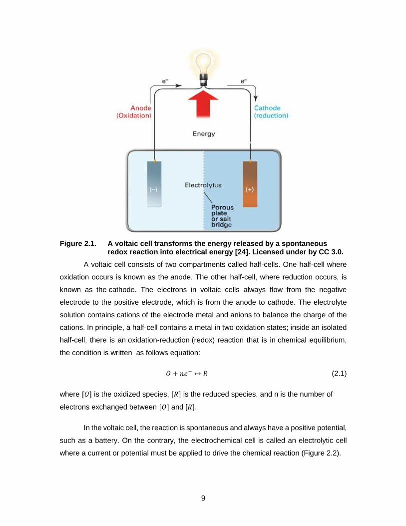
9
Figure 2.1. A voltaic cell transforms the energy released by a spontaneous redox reaction into electrical energy [24]. Licensed under by CC 3.0.
A voltaic cell consists of two compartments called half-cells. One half-cell where
oxidation occurs is known as the anode. The other half-cell, where reduction occurs, is
known as the cathode. The electrons in voltaic cells always flow from the negative
electrode to the positive electrode, which is from the anode to cathode. The electrolyte
solution contains cations of the electrode metal and anions to balance the charge of the
cations. In principle, a half-cell contains a metal in two oxidation states; inside an isolated
half-cell, there is an oxidation-reduction (redox) reaction that is in chemical equilibrium,
the condition is written as follows equation:
𝑂 + 𝑛𝑒− ↔ 𝑅 (2.1)
where [𝑂] is the oxidized species, [𝑅] is the reduced species, and n is the number of
electrons exchanged between [𝑂] and [𝑅].
In the voltaic cell, the reaction is spontaneous and always have a positive potential,
such as a battery. On the contrary, the electrochemical cell is called an electrolytic cell
where a current or potential must be applied to drive the chemical reaction (Figure 2.2).

10
Figure 2.2. An electrolytic cell, an external electrical source is used to generate a potential difference between the electrodes that forces electrons to flow, driving a nonspontaneous redox reaction[24]. Licensed under by CC 3.0.
The electrochemistry deals with cell potential as well as the energy of chemical
reactions. The energy of a chemical system drives the charges to move, and the driving
force gives rise to the cell potential of the cell. The energy aspect is related to the chemical
equilibrium, which is the relationship between the concentration of oxidized species [O],
concentration of reduced species [R], and free energy (∆𝐺[𝐽 ∙ 𝑚𝑜𝑙−1]).
∆𝐺 = ∆𝐺0 + 𝑅𝑇𝑙𝑛[𝑅]
[𝑂] (2.2)
where R is the gas constant (8.314 𝐽 ∙ 𝑚𝑜𝑙−1𝐾−1) and T[K] is the temperature. The critical
aspect of this equation is that the ratio between reduced and oxidized species can be
related to the Gibbs free energy change (∆𝐺), which the half-cell potential (𝐸[𝑉] ) can be
derived as
∆𝐺 = −𝑛𝐹𝐸 (2.3)
11
here 𝐸 is the maximum potential between cathode and anode electrodes, also known as
the open-circuit potential (OCP) or the equilibrium potential, which is present when no
current is flowing through the cell. F is Faraday constant. If the reactant and product have
unit activity, and R is the reaction in the direction of reduction, then equation (2.3) can be
written as
∆𝐺0 = −𝑛𝐹𝐸0 (2.4)
This potential is known as the standard electrode potential (𝐸0[𝑉]). As previously
described, a voltaic cell always deliver a positive potential. It can be explained by the
minus sign in the equation (2.4), thus spontaneous reaction in voltaic cell have a positive
standard electrode potential ( 𝐸0 > 0) . electrochemical cell has a negative standard
electrode potential (𝐸0 < 0).
When combining equations (2.2) - (2.4). All these relationships are tied together in
the concept of Nernst equation. Its mathematical expression describes the correlation
between cell potential and concentration for a cell reaction as:
𝐸 = 𝐸0 +𝑅𝑇
𝑛𝐹𝑙𝑛
[𝑂]
[𝑅] (2.5)
where 𝐸0the standard electrode potential, n is the number of electrons transferred in the
half-reaction, R is the gas constant, T is temperature, and F is the Faraday constant. At
any specific temperature, the Nernst equation derived above can be simplified into a
simple form. At the standard condition of 298 K (25°C), the Nernst equation becomes:
𝐸 = 𝐸0 +0.05916
𝑛𝑙𝑛
[𝑂]
[𝑅] (2.6)
With the know standard electrode potential (𝐸0), the resulting cell voltage (𝐸) can
be used to determine chemical composition in the reaction.
As previously mentioned, anodic currents are generated by ions (anions) diffusing
toward the anode and cathodic currents by ions (cations) diffusing toward the cathode.
The mathematical signs of currents and potentials measured at the anode and cathode
depend on the type of electrochemical cell being investigated. For a reaction to occur
spontaneously, certain conditions must be met, where the free energy change ∆𝐺0 < 0
(𝐸0 > 0) . When a chemical reaction does not occur spontaneously, the cell requires

12
external energy input in order to occur ∆𝐺0 ≥ 0 (𝐸0 < 0). This can be done by applying
potential between electrodes
𝐸𝑐𝑒𝑙𝑙 = 𝐸𝑐𝑎𝑡ℎ𝑜𝑑𝑒 − 𝐸𝑎𝑛𝑜𝑑𝑒 (2.7)
This process is called electrolysis [25]. During electrolysis, the applied potential
can be controlled. The analyte is an electroactive species which can give up or accept
electrons while interacting with the electrochemical cell’s surface.
2.1.1. Electrochemical Cell
Working Electrode
An electrochemical cell consists of two electrodes regardless the type of cell. There
is a working electrode (WE) where the half-cell corresponding to the reaction under study
take place. The working electrode, typically a cathode, represents the most critical
component of an electrochemical cell. The selection of a WE material is critical because
electron transfers occur at the interface between the WE and the analyte solution. Several
important factors should be considered. First, the material should exhibit favorable redox
behavior with the analyte, ideally fast, reproducible electron transfer without electrode
fouling. Secondly, the potential window over which the electrode performs in a given
electrolyte solution should be as broad as possible to allow for the greatest degree of
analyte characterization. Additional considerations include the cost of the material, its
ability to be machined or formed into useful geometries, the ease of surface renewal
following a measurement, and toxicity [25]. Common materials for working electrodes are
platinum, gold, and various forms of carbon, such as glassy carbon and graphite. They
are inert, and, therefore do not participate in the reaction; their sole purpose is to transmit
electrons to and from entities in the solution. WEs sometimes can be chemically modified
in order to increase their sensitivities toward specific species.
Reference Electrode
An electrolytic cell can have either two-electrode or three-electrode configuration.
Regardless the configuration, it must contain a reference electrode (RE), typically an
anode. It holds a stable potential during the redox reaction so that the resulting potential
may be measured with respect to a known potential [25-26]. There are several types of
reference electrodes such as Saturated Calomel Electrode (SCE), silver/silver
13
chloride(Ag/AgCl), mercury/mercurous sulfate (Hg/Hg2SO4) Mercury/Mercury Oxide, and
Normal Hydrogen Electrode (NHE), etc. Mercury based REs possess their disadvantages
because of using Hg which is not biocompatible. Hg/HgO could be used ideally for basic
solutions. In many applications, even a small amount of electrolyte solution leaking from
the reference electrode can immediately compromise the electrochemical reactions.
Primary among these applications is non-aqueous electrochemistry. In these applications,
it may be possible to use what is called a pseudo-reference electrode. The simplest
pseudo-reference electrode is a metal wire, like platinum, inserted directly into the analyte
solution.
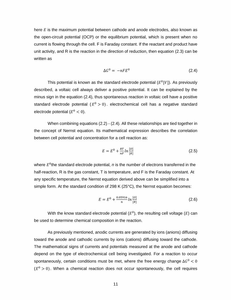
Figure 2.3. Schematic of an Ag/AgCl reference electrode [27]. Licensed under by CC 3.0.
The silver/silver chloride reference electrode is the most regularly used RE duo to
its simplicity, inexpensive design and nontoxic components [27]. The simplicity of the
Ag/AgCl lends many features to make it a great candidate to be used in biomedical and
biosensor applications. Ag/AgCl electrode is a silver wire coated with silver chloride
immersed in a rich 𝐶𝑙− solution (typically saturated KCl solution). If an electron flows to
the electrode, 𝐴𝑔+ from AgCl coating is going to be reduced to Ag and Cl- dissolves into
the solution (Figure 2.3). If electron flows in the reverse direction, Ag coated with AgCl will
give up the electron to get oxidized to 𝐴𝑔+ which later combines with Cl- from the solution
to make insoluble AgCl. The controlling redox process is:

14
𝐴𝑔𝐶𝑙 + 𝑒− ↔ 𝐴𝑔 + 𝐶𝑙− (2.8)
It has a standard potential 𝐸𝐴𝑔/𝐴𝑔𝐶𝑙0 = 0.222𝑉 versus NHE (25℃) [22].
Counter Electrode
The only purpose of the reference electrode is to retain an essentially constant
composition and therefore provides a stable potential. However, in most cases, REs can
be damage by the presence of large current densities and may lose their ideal non-
polarizable behavior. Therefore, a three-electrode configuration is often used in the
modern electrochemical cell. The third electrode called counter electrode (CE) or auxiliary
electrode (AE). The purpose of the counter electrode is to provide a pathway for current
to flow in the electrochemical cell without passing significant current through the RE [28].
There are no specific material requirements for the electrode beyond it not adversely
influencing reactions occurring at the working electrode (WE). Care should be taken that
CE does not interfere with the WE reaction.
Thus when implementing a three-electrode configuration sensor as an
electrochemical cell. A controllable potential is applied between the WE and RE during
electrolysis, while a current run between the WE and CE is monitored. Studying the
relationship between the current and potential, analyte solution can be characterized [28-
29]. The device that applies this potential and monitors the resulting current is called a
potentiostat.
2.1.2. Potentiostat
Simply speaking, potentiostats are amplifiers used to control a voltage between
two electrodes (WE and RE) to a constant value or patterns. Figure 2.4 shows a principle
schematic diagram for a potentiostat. The potential of the working electrode is measured
relative to a constant-potential reference electrode that is connected to the WE through a
high-impedance potentiometer E. To set the WE’s potential constantly, a feedback loop
control is essential. If the working electrode’s potential begins to drift, the feedback
amplifier can return the potential to its initial value. The current flowing between the CE
and the WE is measured with an ammeter. Modern potentiostats include waveform
generators that allow us to apply a time-dependent potential profile, such as a series of
potential sweep pattern to the working electrode.

15
Figure 2.4. Schematic diagram of a general potentiostat and connection with an electrochemical cell
2.1.3. Method of Analysis
Electrochemical techniques can be classified into several categories depending on
the experimental conditions and the analytical signal. In a static technique, no current is
allowed to pass through the analyte’s solution. Dynamic techniques, in which current is
allowed to flow through the analyte’s solution. Figure 2.5 provides one version of a
summary highlighting the experimental conditions, the analytical signal, and the
corresponding electrochemical techniques. Among the experimental conditions under
control are potential or the current, and whether the analyte solution is stirred [29]. Among
them, amperometry and voltammetry, in which we measure current as a function of a fixed
or variable potential, are the most important quantitative electrochemical methods.

16
Figure 2.5 Summary of interfacial electrochemical techniques. The specific techniques are shown in red, the experimental conditions are shown in blue, and the analytical signals are shown in green [24]. By LibreTexts is licensed under CC 3.0.
Amperometry in biosensor is the study of the current response or change in current
response based on analyte concentration when a certain potential is applied. For

17
electrochemical detections, amperometry could be defined as change in current response
due to presence of electrons in the solution. Either way, it’s the change in current response
when a fixed step potential is applied. In general, amperometry is the measurement of
electrode current between a pair of electrodes that are driving an electrolysis reaction. In
this reaction, the reactants is the intended analyte and the measured current is
proportional to the concentration of the analyte.
In order to grasp what is taking place in amperometry, the concept of how the
current changes when a stimulus is applied must be understood. As previously described,
Nernst equation predicts the relationship between the potential of an electrochemical cell
and concertation of analyte species. When we oxidize an analyte at the WE, the resulting
electrons pass through the potentiostat to the CE, reducing the solvent or some other
component of the solution matrix. If we reduce the analyte at the WE, the current flows
from the CE to the cathode. In either case, the current from redox reactions at the WE to
CE is called a faradaic current. In an unperturbed solution, when a potential step is applied
that causes as surface reaction to occur, the current decays according to the equation
called Cottrell equation as [30]:
i = 𝑛𝐹𝐴𝐷0
1/2𝐶0
∗
𝜋1/2𝑡1/2 (2.9)
where 𝐷0 is the diffusion coefficient for the species, A is the surface area of electrode, n
is the number of electrons transferred per electroactive molecule or ion, 𝐶0 is the
concentration of the oxidized species in mol cm3⁄ and t is the time in seconds.
There are four major factors that effect the reaction rate and current at electrodes:
(i) mass transfer to the electrode surface (ii) kinetics of electron transfer; (iii) preceding
and ensuing reaction; (iv)surface reactions. The slowest process will be the rate-
determining step [30]. As shown in Figure 2.6, the simple redox reaction may be
considered as a set of equilibria involved in the migration of the reactant toward the
electrode, the reaction at the electrode, and the migration of the product away from the
electrode surface into the bulk of the solution [30].

18
Figure 2.6. Close look of reaction at surface of electrode, both chemical transfer and mass transfer are involved [29]. Reprinted with permission.
Unfortunately, amperometry cannot determine the kinetics of the electron transfer
and hence the kinetics of the reaction. That is, it cannot determine whether a surface
confined or diffusion controlled reaction has occurred; information obtained from
amperometry is limited compared to that of voltammetry.
On the contrary, voltammetry is an electrochemical technique to study current
response as a function of applied voltage to the electrolytic cell; or in simple words- current
response at varying potential. Cyclic voltammetry (CV) is perhaps the most versatile
electroanalytical technique for the study of electroactive species and is often the first
experiment performed in an electrochemical study of a compound, biological material, or
an electrode surface. The effectiveness of CV results from its capability for rapidly
observing the redox behavior over a wide potential range. The resulting voltammogram is
analogous to a conventional spectrum in that it conveys information as a function of an
energy scan. The cyclic voltammetry completes a scan in both directions in either to more
positive potentials or more negative potentials. Figure 2.7a shows a typical potential-
excitation signal; the potential is first scanned to more positive values, resulting in the
oxidation reaction for the species R. This is known as forward scan in equation (2.2). When
the potential reaches a predetermined potential value, the direction of the scan is reversed
toward more negative potentials. The species O is generated on the forward scan, during
the reverse scan it is reduced back to R. This is known as reverse scan in equation (2.1)

19
Because cyclic voltammetry is carried out in an unstirred solution, the resulting CV,
as shown in Figure 2.7, has peak currents. As the voltage is decreased and swept towards
the reduction potential of the system, electron transfer between the electrode and the
oxidized species begins. This current continues to increase until a cathodic peak 𝑖𝑝,𝑐 is
observed, corresponding to a peak potential of 𝐸𝑝,𝑐 . Past this potential, the oxidized
species becomes depleted and the current decreases [24]. The voltage is then reversed
and swept towards the oxidation potential. This change in potential forces the reverse
reaction whereby the reduced species becomes oxidized, resulting in an anodic current
peak 𝑖𝑝,𝑎 at 𝐸𝑝,𝑎.
Figure 2.2.7. Typical potential sweep execution signal (A) and an ideal CV curve (B) [24]. By LibreTexts is licensed under CC 3.0.
The peak current in cyclic voltammetry can be predicted by Randles-Sevcik equation
[29]
𝑖𝑝 = 2.69 × 10⁵𝑛3/2𝐴𝐷1/2𝐶𝑣1/2 (2.10)
where n is the number of electrons in the redox reaction, A is the area of the working
electrode, D is the diffusion coefficient for the electroactive species, ν is the scan rate,
and C is the concentration of the electroactive species at the electrode. For a well-
behaved system, the anodic and cathodic peak currents are equal, and the ratio 𝑖𝑝,𝑎/𝑖𝑝,𝐶 is
1.00. The half-wave potential, 𝐸0 , is midway between the anodic and cathodic peak
potentials.
𝐸0 =𝐸𝑝,𝑎+𝐸𝑝,𝐶
2 (2.11)

20
Scanning the potential in both directions provides users with the opportunity to
study the electrochemical behavior of species generated at the electrode. This is a distinct
advantage of cyclic voltammetry over other voltammetric techniques. Figure2.8 shows the
cyclic voltammogram for the same redox couple at both a faster and a slower scan rate.
At the faster scan rate we see two peaks in Figure 2.8A. At the slower scan rate in Figure
2.8B, however, the peak on the reverse scan disappears. One explanation for this is that
the products from the reduction of R on the forward scan have sufficient time to participate
in a chemical reaction whose products are not electroactive [30].
Figure 2.8. Cyclic voltammograms for R obtained at (A) a faster scan rate and (B) a slower scan rate [24]. By LibreTexts is licensed under CC 3.0.

21
2.1.4. Biosensor and Principle of Lactate Sensing
Biosensors are used for the detection of biological analytes, such as lactate. The
development of the first biosensor is closely associated with the names of Leland C. Clark
and Champ Lyons. Clark and Lyons created the first enzyme based glucose biosensor at
the Cincinnati Children's Hospital in 1962 [31]. The primary structure of a biosensor
includes two main elements, the biological element, and the transducer element. These
two elements are connected to an electronic display that converts the signal into a
readable format for the viewer. The biological recognition element (number 2 in Figure
2.9) detects the desired analyte (number 3 in Figure 2.9). The desired analyte can be any
biological element, from nucleic acids to proteins. This is a selective element that should
only detect the desired analyte [32-36]. The biological element is what drives the selection
of the transducer element. The transducer converts the biological event into an electrical
signal. The transducer element can be electrochemical or biological. Electrochemical
transducers include nanotubes and nanoparticles while biological transducers include
enzymes other biological components [37]. Transducers can be combined to strengthen
the biosensor's signal. The signal is then amplified and sent to a display where it is
processed into a readable format for the viewer to use.
Figure 2.9. Illustration of the immobilized enzyme [29]. Reprinted with permission.
Lactate is the conjugate base of a lactic acid, also known as 2-hydroxy propanoic
acid. Being produced continuously from pyruvate. Lactate plays a cardinal role in several
biochemical processes. Hence lactate could be found in body fluids such as saliva [38],
interstitial fluids [39], tear [40] and exhaled breath [41]. Lactate could as well be found in
urine and sweat [42]. Sweat demonstrates a great prospect for continuous lactate
measurement being easily accessible to offer real-time physiological information. Sweat

22
is composed of various dissolved salts, lactate, urea, amino acids, bicarbonate, etc. [43-
48]. Human perspiration has been estimated to contain at least 61 different constituents
with varying concentrations. During normal metabolism, eccrine sweat gland obtains ATP
through oxidative phosphorylation. Under conditions such as ischemia or anaerobic
metabolism, glycolysis becomes the main pathway to produce ATP and gives rise to
lactate. The intensive exercise ends up leading to increasing in lactate production in sweat
from ~10 mM to as high as ~25 mM [49-50]. Therefore, lactate sensors can be useful for
measuring lactate level in sports medicine. The quest for non-invasive and continuous
lactate monitoring led researches to search for utilizing alternative body fluids. In an article
entitled, “Bendable Electro-chemical Lactate Sensor Printed with Silver Nanoparticles” by
M. A. Abrar outlines a flexible amperometric biosensor based on silver nanoparticles for
monitoring lactate concentration utilizing perspiration along with the demonstrate an
immobilization procedure of enzyme [22]. Lactate oxidase (LOD) enzyme was used for
lactate measurement due to its reaction simplicity and easy biosensor design. As the
name suggests, Lactate Oxidase (LOD) is an enzyme which catalyzes lactate by oxidation
to produce pyruvate. The enzyme can be reoxidized in the presence of O2 to release
hydrogen peroxide (H2O2). H2O2 gets oxidized at the electrode surface, restores O2
concentration and gives a current proportional to the amount of lactate. Reactions involved
in LOD-based sensor could be summarized as [22]:
𝐿 − 𝑙𝑎𝑐𝑡𝑎𝑡𝑒 + 𝐿𝑂𝐷𝑜𝑥 → 𝑝𝑦𝑟𝑢𝑣𝑎𝑡𝑒 + 𝐿𝑂𝐷𝑟𝑒𝑑 (2.12)
𝐿𝑂𝐷𝑟𝑒𝑑 + 𝑂2 → 𝐿𝑂𝐷𝑜𝑥 + 𝐻2𝑂2 (2.13)
𝐻2𝑂2 → 𝑂2 + 2𝐻+ + 2𝑒− (2.14)
The oxidation reaction of H2O2 that occurs on the electrode's surface allows the
biosensor to detect the lactate concentration by the current it produces. The current given
off by the electrode is linearly proportional to the H2O2 concentration. Because the
enzymatic induced reaction has a one-to-one molar ratio of L-lactate and H2O2, the current
recorded by the biosensor is also proportional to the detected the lactate concentration.
Therefore, the lactate concentration is also linearly proportional to the current given off by
the electrode.

23
2.2. 3D Printing Technologies for Sensors and Electronics
In this section, a brief review of existing techniques of 3D printing is introduced
along with an overview of current 3D-printed sensors and electronics. The advantages
and limitations in the different 3D fabricating processes are discussed in order to select
the best method for 3D-PCB and sensor printing.
2.2.1. Current 3D Printing Technology
The 3D-printing process starts with a digital model of the object. Its digital virtual
model can be generated using a three-dimensional scanner, computer-aided design
(CAD) software, or by photogrammetric technology. Then 3D model needs to be converted
into an STL file. This STL file contains a list of coordinates of triangulated sections which
store the information about the model’s surfaces. All 3D printer software can read STL
files, and then slice the object to obtain a series of 2D cross section layers by a Z direction
discrete approach. Finally, the desired 3D object is created using layer by layer printing.
A specific 3D printing process is shown in Figure 2.10 [51].
Figure 2.10. 3D-printing process. A digital model of the object is obtained through CAD software or 3D scanner. The 3D model design is then converted to the STL format to G-code file. Finally, the printer starts depositing the material following the layer-by-layer sequence [51]. Reprinted with permission.

24
Depending on the manufacturing principles and materials, 3D printing technologies
can be divided into six main categories: fused deposition modeling (FDM), directly ink
writing (DIW), laser-based stereolithography (SLA) and digital light processing (DLP),
Laminated object manufacturing (LOM), laser sintering and laser melting (SLS, SLM), and
photopolymer jetting (Ployjet) [52-63].
2.2.1.1 Fused Deposition Modeling (FDM)
FDM was first introduced by Crump [52]. The working principle of FDM 3D printers
involves melting and extruding a thermoplastic filament through a nozzle (Figure 2.11).
The melted material deposited on the fabrication platform then cools down and solidifies,
and this process is repeated in a layer-by-layer fashion to build up a 3D structure.
Thermoplastic materials such as polyamide (PA), polylactic acid (PLA), acrylonitrile
butadiene styrene (ABS), polycarbonate (PC), etc. are usually employed and provided as
a filament for FDM 3D printers [53]. FDM has been widely used for its low material cost
and open source nature, but it is limited by its low printing resolution and slow printing
speed.
Figure 2.11. Schematic diagram of fused deposition modeling (FDM). A nozzle fed with a thermoplastic wire is moved in three dimensions across the building platform onto which molten voxels of a polymer are applied [51]. Reprinted with permission.
25
2.2.1.2Direct Ink Writing (DIW)
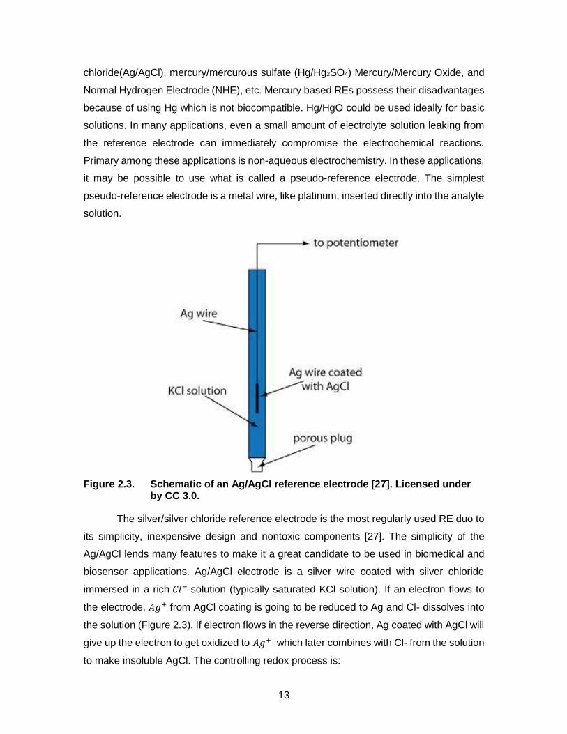
Direct ink writing printers use nozzles that directly extrude materials onto a
fabrication platform (Figure 2.12). This technology allows the controlled deposition of
materials in a highly viscous liquid state, which allows them to retain their shape after
deposition. Direct ink writing technology is extremely versatile because a large variety of
materials can be deposited, ranging from ceramics, plastics, foods, hydrogels and
conductive ink [53-54]. The nozzle size, viscosity, and density of the material, scanning
speed, eject speed, and other parameters can be adjusted to obtain an optimal deposition
object. A post-fabrication process may need to harden the created object and improve its
mechanical properties via sintering, heating, UV curing and drying step.
Figure 2.12. Schematic diagram of direct ink writing. A material dispenser connected to a computer-controlled robot, scans across the building platform, depositing the ink material in a layer-by-layer manner[51]. Reprinted with permission.

26
2.2.1.3. Photocuring (SLA, DLP)
Photocuring uses ultraviolet (UV) light to cure liquid polymers in a layer-by-layer
manner, building 3D structures on the platform. There are two types of photocuring
technologies: stereo lithography apparatus (SLA) [55] and digital light processing (DLP)
[56].
Figure 2.13. (A) Stereolithography (SLA) in a bath configuration where a laser beam is scanned across the liquid surface to polymerize the resin. Successive layers are created by lowering the movable table, allowing the fresh liquid resin to be exposed. (B) DLP in a layer configuration in which a laser beam is scanned from the bottom of the liquid tank through a transparent window. The polymerized layer attaches to the table, which is then moved upwards to refill the gap between the first layer and the window with fresh resin[51]. Reprinted with permission.

27
Figure 2.13A shows the fundamental principle of SLA. A tank is filled with a liquid
photosensitive resin, which changes from liquid to solid when exposed to a certain
ultraviolet light wavelength. The laser scanning of the layered cross section under the
control of the computer leaves the layer cured. The cured layer is covered with a layer of
the liquid resin after the platform reduces the height of a layer. [57]. Then a new layer is
ready to be scanned, and the new cured layer is firmly glued on the preceding layer. The
steps above are repeated until all the parts of the digital model are completed, and a 3D
model is obtained. SLA cures the photosensitive resin by means of a moving laser directly,
whereas DLP uses a laser or UV lamp as the light source. The light shines through special
patterns on a digital mirror device, then the exposed parts are cured and a layer is finished.
The platform rises a height of a layer and the next exposure period starts. A 3D solid model
is obtained when all the layer have been exposed to the light [58]. Figure 2.13B shows
the fundamental principle of DLP. The digital mirror device used as a dynamic mask is the
main difference between SLA and DLP. SLA and DLP can produce highly accurate
structures with complex internal features, but have the disadvantage of being limited to
the use of a single-material.
28
2.2.1.4. Lamination (LOM)
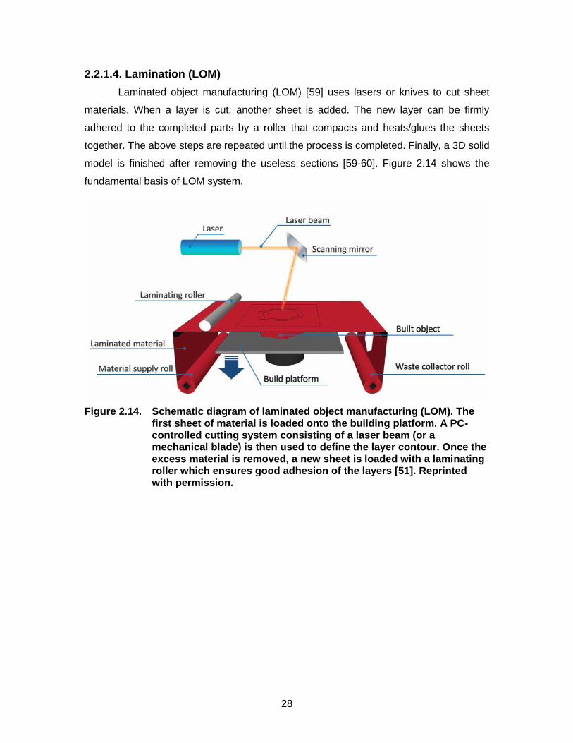
Laminated object manufacturing (LOM) [59] uses lasers or knives to cut sheet
materials. When a layer is cut, another sheet is added. The new layer can be firmly
adhered to the completed parts by a roller that compacts and heats/glues the sheets
together. The above steps are repeated until the process is completed. Finally, a 3D solid
model is finished after removing the useless sections [59-60]. Figure 2.14 shows the
fundamental basis of LOM system.
Figure 2.14. Schematic diagram of laminated object manufacturing (LOM). The first sheet of material is loaded onto the building platform. A PC-controlled cutting system consisting of a laser beam (or a mechanical blade) is then used to define the layer contour. Once the excess material is removed, a new sheet is loaded with a laminating roller which ensures good adhesion of the layers [51]. Reprinted with permission.
29
2.2.1.5. Selective Laser Sintering and Selective Laser Melting (SLS, SLM)
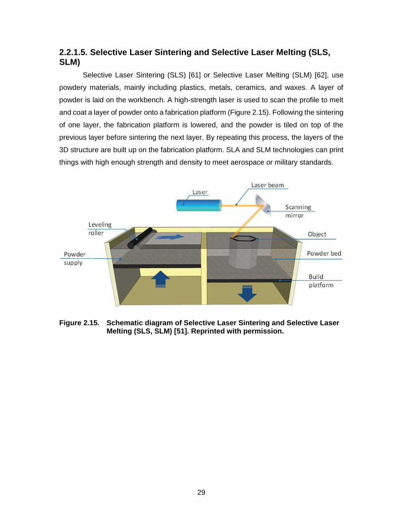
Selective Laser Sintering (SLS) [61] or Selective Laser Melting (SLM) [62], use
powdery materials, mainly including plastics, metals, ceramics, and waxes. A layer of
powder is laid on the workbench. A high-strength laser is used to scan the profile to melt
and coat a layer of powder onto a fabrication platform (Figure 2.15). Following the sintering
of one layer, the fabrication platform is lowered, and the powder is tiled on top of the
previous layer before sintering the next layer. By repeating this process, the layers of the
3D structure are built up on the fabrication platform. SLA and SLM technologies can print
things with high enough strength and density to meet aerospace or military standards.
Figure 2.15. Schematic diagram of Selective Laser Sintering and Selective Laser Melting (SLS, SLM) [51]. Reprinted with permission.

30
2.2.1.6. Photopolymer Jetting (Ployjet)
Photopolymer jetting was originally introduced by Gothait [63]. For Ployjet, a
photosensitive resin is used as printing material. This photosensitive resin is ejected from
an inkjet nozzle and deposited on a mobile platform, then cured by UV light and solidified
(Figure 2.16). This approach allows layer-by-layer fabrication. A 3D product can be
obtained after curing all layers of the entire model. This method can print products with
multiple materials and colors simultaneously. Ployjet is suitable for printing small and
delicate objects due to its high-resolution. The strength of parts produced by this process
is however weak.
Figure 2.16. Schematic diagram of Photopolymer jetting (Ployjet) [51]. Reprinted with permission.

31
Table 2.1. Summary of each printing methods
Technique Principle Material Advantage Limitation
Fused deposition modeling (FDM)
Extrusion-based
Thermoplastics (ABS, PLA, PC, PA, etc.); glass (new); eutectic metal; ceramics; edible material, etc.
Simple using and maintaining; easily accessible; multi-material structures; low cost
Rough surface low resolution; high cost (for glass and metal)
Directly ink writing (DIW)
Extrusion-based
Plastics, ceramic, food, living cells, composites
Versatile Low resolution; requires post-processing
Stereo lithography apparatus(SLA) & (Digital light procession)DLP
Photocuring Photopolymers High accuracy; simple
Single material; biocompatible
Laminated object manufacturing (LOM)
Lamination Sheet material (paper, plastic film, metal sheets, cellulose, etc.)
Versatile; low cost; easy to fabricate large parts
Time-consuming; limited mechanical properties; low material utilization; design limitations
Selective laser sintering(SLS) Selective laser melting(SLM)
Powder based laser curing
Powdered plastic, metal, ceramic, PC, PVC, ABS wax, acrylic styrene, etc.
High accuracy; wide adaptation of materials; high strength
Limited mechanical properties; high cost
Photopolymer jetting(Ployjet)
Inkjet-based Liquid photopolymers High accuracy High cost

32
2.2.2. 3D Biosensor Applications
Table 2.2. Summary of 3D-printed sensors
Application of Sensor
Method Material Transduction Mechanism
Ref.
Strain sensors
DIW Carbon-based ink Resistance [64]
LOM Silicone rubber Resistance [65]
DIW Graphene aerogel Resistance [66]
Pressure sensors
FDM ABS-based material Capacitance [67]
FDM PVDF Capacitance [68]
FDM ABS Optical absorbance [69]
Accelerometers 3DP Silver nanoparticles Capacitance [70]
FDM,SLA Thermoplastics Gravity [71]
EEG sensors FDM PLA, ABS Resistance [72]
FDM PLA Resistance [73]
Antennas
DIW Silver nanoparticle ink RF reception [74]
FDM Dupont 5064H RF reception [69]
3DP EPOLAM resin RF reception [75]
SLA Steel Patch antenna [76]
inkjet Silver nanoink Patch antenna [77]
Biosensors DLP Spot-A materials Chemiluminescent [78]
DIW PDMS, Hydrogel Resistance [79]
Temperature sensors
Inkjet printed Exfoliated graphite and latex solution
Resistance [80]
SLA Photopolymer Electro-chemiluminescence
[81]
The greatest difference between biosensors and other sensors is that the signal
detection of biosensors contains sensitive layers such as an enzyme. In recent decades,
we have witnessed a tremendous number of activities in the area of biosensors. Due to
characteristics such as intelligence, miniaturization, and specificity, biosensors offer
exciting opportunities for researchers and corporations in applications from situ analysis
to home self-testing. The biomaterial patterning of biosensor fabrication is one of the most
promising techniques for improving biosensor stability. 3D-printing technology is reliable
and efficient for facilitating controllability over the entire process and represents an
authentic breakthrough for the development and mass production of biosensors. A
detailed summary of 3D sensors including 3D printing technologies, transduction
mechanism, application, printing materials is listed in Table 2. Among them, flexible
electrochemical sensors were reported previously fabricated by conducting polymers
inorganic, and carbon nanotubes [82-88] have been reported. Conventional fabrication
approaches mostly involve screen-printing which produce electrode pattern. A flexible
amperometric lactate biosensor using silver nanoparticle (AgNP)-based conductive

33
electrodes have been reported. This biosensor is designed and fabricated by modifying
silver electrode with lactate oxidase immobilized by bovine serum albumin (BSA). The
silver electrodes are fabricated via stamping in conjunction with a simple spray coating of
AgNP ink [88]. AgNP inks normally have low resistance in order of 10−6Ω/𝑐𝑚 [84]. Figure
2.17 summarizes conductivity of conductive materials including bulk silver, copper, and
solder alloy which are not easy to be adapted in 3D-printed electronics. AgNP inks show
a great potential in 3D-printing.
2.2.3. 3D Electronics Applications
3D printing technologies have also been expanded to electronics field as early
stage. Previous works such as inkjet printing, directly fused deposition modeling (FDM)
[89], and 3D molded interconnect device technology (3d-MID) [90]. Several 3D
technologies have been demonstrated for patterning of electronic circuits. The
combination of direct writing of conductive inks onto solid freeform fabricated structures
was introduced by Palmer et al. [91] and Medina et al. [92], in which modest circuits were
implemented to demonstrate functionality by integrating a dispensing system into a
stereolithography (SL) machine using 3D linear stages with a dispensing head. Lopes et
al. [92] demonstrated a simple prototype temperature sensor with nine components
including an integrated circuit in a low-pin-density package, and in the same fashion.
Others have demonstrated a similar circuit as well as several clever electromechanical
applications all created by an open-source fabrication system [91–93]. Navarrete et al.
[93] described improvements to conductor density by introducing channels into the SL
substrate for containing the conductive material in order to reduce the possibility of line-
to-line shorting and improve the cross-sectional area for improved performance. Line
spacing was thus controlled by the precision of the SL laser beam as opposed to the
dispensing system. Additionally, this demonstration included not only digital logic and
control but also radio frequency (RF) wireless functionality [94]. The system was
implemented in the form of a hidden-in-plain site rock to highlight the possibility of
fabricating a line of systems—each of which could be altered in CAD to provide unique
form similar to a snowflake and aiding in the deception by providing irregularities among
the sensor systems. Ram et al. [95] reported electronics embedded in 3D-printed metal
structures. More recently, collaborative work performed by Stratasys and Optomec

34
reported the use of FDM with aerosol-sprayed conductors but used large pin pitch
packaging [96, 97]. Most of the reported circuits to date fall into three categories:
Firstly, direct writing of viscoelastic conductive metallic nano materials such as
silver nanoparticle ink to form passive RLC radio-frequency electronic in small-scale,
which can be resonated into certain frequency bandwidth by varying printed RLC
demission. Secondly, a hybrid additive manufacturing process involves the fused
deposition modeling of the thermal plastic substrate structure, and direct embedding of a
conductive material has been demonstrated. This type of AM technology can fabricate a
substrate in any arbitrary form, while the embedded conductive material is used as
electrical interconnects through the precise printing of conductive inks or wires to realize
circuit traces between components. Thus, functional 3D-printed electronic devices can be
achieved by utilizing this capability along with insertion of electronic components include
microchips, batteries, and antennas. Thirdly, a conductive ink, in most cases, the
conductive AgNP ink is ink-jetted or screen printed into desired flat circuit trace pattern on
flexible substrates. Thus, the complex circuit design can be achieved by stacking multiple
circuit layers through interconnecting vias. This process type is more accurately described
as a 2D layered electronic device.
All the previously reported 3D-printed electronics from fabrication above
technologies show the capability to perform electronic functions. However, the majority of
these printed circuits are used for the very preliminary electronic task, such as blink LEDs
[88-90], because little of these 3D-printed electronics actually realize sophisticated circuit
design comparable to a conventionally embedded electronic devices. An electronic device
typically composed of several ICs and passive components in a compact design includes
a low power microcontroller unit (MCU), a power supply, a voltage regulator, a
communication chip, and many inductors, resistors, and capacitors. In order to integrate
these components, PCB with high density interconnect (HDI) based assemblies are
commonly used to build such systems using small surface mount devices (SMD). Only a
few of 3D-printed electronics PCBs have been demonstrated with a high density of ICs
(Figure 2.18).

35
Figure 2.17. 3D printed electronics (a)magnetic flux sensor system with curved surfaces and modern miniaturized electronic components[98] (b)CubeSat 3D-printed module produced by using stereolithography and direct print technologies[98] (c) 3D-printed CubeSat module produced by using fused deposition modeling [98]. Reprinted with permission.
Given the tight dimensional requirements of electronic components including pin
pitch and miniaturized package volume, the 3D-PCB fabrication technology must provide
high spatial resolution. Whereas stereolithography has sufficient spatial resolution given
the small beam width of the laser, FDM produces feature sizes at or larger than 254 μm
and is not small enough to deliver circuit pad for regular IC components in electronics
fabrication. For example, with a 0.65-mm pitch 144-pin TQFP package common in
contemporary electronics, the chip cavity requires a flush encapsulation with pin features
including 450-μm openings with 200-μm separation fins—to provide mechanical support
and electrical access to the packaged silicon. Therefore, to provide the feature resolution
necessary in the context of FDM fabrication, the multi3D system implements additional
high-resolution subtractive methods. When conductive inks are still appropriate, the PCB
substrate must have superior surface finish with minimal porosity—otherwise, the porosity
will result in shorts between electrical lines as the conductive inks will spread before
curing. Consequently, the multi3D system includes FDM build parameter for printing with
improved density to maintain separation of conductive ink traces. In cases where the
interconnect is required to provide high current densities with bulk level conductivity
(1.6810−6 Ω 𝑐𝑚⁄ as a reference), wires can be introduced providing performance which is
impossible to achieve with cured conductive inks (or even the solder-based approach
described previously). In the multi3D system, wires are embedded with a novel patent-
pending thermal embedding technique that submerges wires as small as 80 μm in
diameter firmly into the thermoplastic substrates fabricated with FDM—leaving a planar
surface to continue the interrupted fabrication process.

36
2.2.4. Conductive Nano-Material Printing
There are several challenges which should be overcome while using conductive
NPs as the functional component of conductive inks. First, NPs in ink should be stable
against aggregation and precipitation to provide reproducible performance. Therefore, the
addition of a stabilizing agent, which is usually a polymeric material or a surfactant, is
required. This stabilizer is especially important for dispersions with high metal loading, 20–
60 wt%, which are required for obtaining printed patterns with a high density of metal to
provide high conductivities.
Furthermore, NPs-based conductive inks should provide good electrical
conductivity of printed patterns. It is obvious that the best candidates for conductive
material are the highly conductive metals, such as Ag (σ = 6.3 · 10−7Ω/𝑐𝑚), Cu ( σ = 5.96
· 10−7Ω/𝑐𝑚), Au ( σ = 4.42· 10−7Ω/𝑐𝑚), and Al ( σ = 3.78 · 10−7Ω/𝑐𝑚). Currently, silver is
the most reported material for conductive ink, and also the most utilized in industrial
applications. Due to their high cost, a major challenge in this field is to replace silver and
other noble metals with cheaper ones, such as copper and aluminum. This would depend
on the success in avoiding their oxidation at ambient conditions, otherwise an inert
atmosphere would be required.
Another challenge in using metallic nanoparticles is the need for a post-printing
process in order to sinter the NPs for obtaining continuous metallic phase, with numerous
percolation paths between metal particles within the printed patterns. This is usually an
obligatory stage since the presence of stabilizing agents and other ink components
prevents close electrical contacts of NPs due to the existence of organic insulation layers
that surround the NPs. The conventional approach for sintering metallic NPs is heating.
However, in the case of heat-sensitive substrates (e.g., paper, plastics), heating at
temperatures above 120–150℃ is not applicable and, therefore, non-destructive methods
of sintering are required.
Nanoparticles can also be used for effective electrical wiring of LDH or LOD
enzyme for L-lactate detection. Various nanomaterials such as carbon nanotubes(CNT)
and gold(Au) nanoparticles have been used as electrical connectors between the
electrode and the redox center of the enzyme. A wide variety of nanoparticles has been
used in lactate biosensors due to their advantage both regarding stability and in improving

37
the sensitivity. As a result of valuable properties of large surface- to-volume ratio, excellent
surface reaction activity, high electro catalytic efficiency and highly adsorbing property,
nanomaterials are an important candidate for enzyme immobilization in the fabrication of
lactate biosensors.
Silver nanowires (AgNWs) and nanoparticles (AgNPs) have been extensively
studied for fabricating stretchable electrodes lately. Silver (Ag) is known to be the best
conductive metal, and it is also cheaper compared to noble metals such as gold or
platinum. It is chemically more stable in air than copper and aluminum, syntheses of
AgNWs and AgNPs have been well-established. The lower sintering temperature
promotes easiness of a manufacturing process, for example, a sintering temperature of
bulk gold is 1,063 °C while it is only about 130 °C with gold nanoparticles in 2 nm size
Also, the addition of conductive nano-fillers in a polymeric matrix can provide an electrical
property to the composite. Enormous kinds of conductive nano-composite composed of
various fillers have been reported as an alternative for using conductive bulk metals or
alloys thanks to the previously stated advantages brought by nanomaterials. Silver
nanomaterials have been demonstrated to design and fabricate highly conductive
electrode for stretchable electronics [101-107].
Figure 2.18. Electrical resistivity properties of conductive materials [101-107]
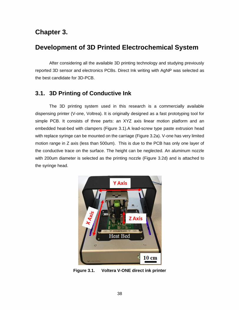
38
Chapter 3. Development of 3D Printed Electrochemical System
After considering all the available 3D printing technology and studying previously
reported 3D sensor and electronics PCBs. Direct Ink writing with AgNP was selected as
the best candidate for 3D-PCB.
3.1. 3D Printing of Conductive Ink
The 3D printing system used in this research is a commercially available
dispensing printer (V-one, Voltrea). It is originally designed as a fast prototyping tool for
simple PCB. It consists of three parts: an XYZ axis linear motion platform and an
embedded heat-bed with clampers (Figure 3.1).A lead-screw type paste extrusion head
with replace syringe can be mounted on the carriage (Figure 3.2a). V-one has very limited
motion range in Z axis (less than 500um). This is due to the PCB has only one layer of
the conductive trace on the surface. The height can be neglected. An aluminum nozzle
with 200um diameter is selected as the printing nozzle (Figure 3.2d) and is attached to
the syringe head.
Figure 3.1. Voltera V-ONE direct ink printer

39
Figure 3.2. Direct ink writing mechanism detail
A silver nanoparticle ink is used as the conductive ink for printing. It has high
electrical conductive and high viscosity. These properties ensure users can control the
dispensed ink shape through a tiny nozzle. The control of the V-one printer is done with
an interface software (Voltera). The purpose is to convert the conventional PCB Gerber
file from any PCB design software to a machine recognized g-code. The user can import
their PCB file, such as.GTL (Gerber top layer) and.TXT (drill file) to the Voltera interface
software. Then the geometry design can be sliced depending on slice parameters (feeding
and gap). As previously mentioned, the nozzle has 200 um diameter, which means the
width of each single dispensed ink trace us 200 um. For regular PCB trace, average width
is 12 mil, which is around 300 um. Thus one or two slices can be generated. For much
bulk part, such as a large electrode and conductive pads, more slices is generated to fulfill
the necessary area (Figure 3.3). The XYZ motion of extrusion head is executed by three
servo motors via conveyor belt. The resolution of each axial motion is 50 um.
Figure 3.3. Voltera Software Slicing Feature of SMD circuit pattern (left) SMD QFN28 footprint (middle) sliced STI file with 0.15 line space (right) 0.1 line space.

40
3.2. Building Processes for PCB Printing
Figure 3.4. Flow chart of the additive manufacturing of- of 3D printed PCB

41
3.2.1. Pre-calibration
Considering a simple electronics with a single layer double sided PCB. There are
several steps involved in 3D printing using V-one. After interface software converts PCB
Gerber Top Layer file (GTL). A clean and flat substrate is placed and clamped on the heat
bed area, no heat is applied at this moment. The detection probe is mounted XYZ motion
platform first. The purpose is to calibrate the substrate surface height and position by
contacting multiple checking points on the substrate surface. These checkings are all
located on the path of circuit trace and pads. In this way, a temporary height profile in Z
axis is generated in case the substrate is not flat (Figure 3.5).The second step is removing
the probe and mounting the lead screw extrusion head with Ag conductive ink syringe.
One thing should be noticed that all the air left inside of nozzle tip must be pushed out.
Otherwise, it can cause discontinuity of printed ink. Manually rotating the lead screw can
provide pressure inside of syringe. Thus conductive ink can be pushed out. However, too
much pressure will cause excess ink keeping leaking. (Figure 3.6).Therefore extra
attention must be paid.
Figure 3.5. Calibration procedures for substrate height profile
Figure 3.6. Ink level calibration procedure before printing

42
3.2.2. Top Layer Circuit Printing
Now V-one is ready to 3D print the PCB. Silver conductive ink is dispensed on the
top layer of the substrate. First, the extrusion head is controlled by the motion platform
which follows the sliced g-code in the software. This is a straight-forward procedure. After
the top layer circuit is fully printed, the extrusion head and ink syringe are removed from
the platform. At this moment, the printed ink is not conductive yet. Therefore the next step
is baking the printed circuit trace on the embedded heat bed. The temperature and time
are the important parameters and can be varied in the interface software depending on
the substrate material property. The detail is explained next section. The baking process
sinters Ag Nanoparticle and thus generates the conductive path.
Figure 3.7. Top layer circuit printing procedure
3.2.3. Drilling
As previously mentioned, V-one leaves a donut geometry for any via and through-
hole design (Figure 3.8). In order to make sure the bottom side circuit can be printed in
the correct alignment with a top side, the drilling is necessary before printing bottom side
circuit. In general PCB design, via the through-hole diameters are from 8mil to 12mil, only
6mil or even smaller in some extreme designs. A high-speed press driller (Dermer)(Figure
3.9a) and standard PCB driller bit kit (Figure 3.9b) are used in the drilling process. The
donut ring is easy for manually drilling without requiring the CNC drilling. In the time-
efficient point of view, this is a great advantage (Figure 3.9c).

43
Figure 3.8. Circuit patterns of through-hole, vias, and pads for printing
Figure 3.9. (left) Dermer Mode 3000 press driller (middle) PCB drill bits set (right) image of drilling process for through-hole and vias
3.2.4. Bottom Layer Circuit Printing
There is one more calibration that must be done before actually printing the bottom
layer circuit. As commonly known, circuits on the top layer and bottom layer are
interconnected by the vias. Thus, any mismatch of the position of the printed circuit will
ruin the whole 3D-PCB. It is crucial to make sure that every single via on bottom layer is
aligned with drilled vias.
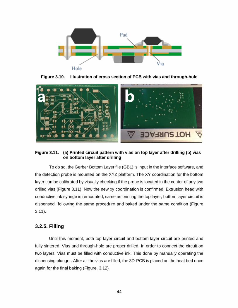
44
Figure 3.10. Illustration of cross section of PCB with vias and through-hole
Figure 3.11. (a) Printed circuit pattern with vias on top layer after drilling (b) vias on bottom layer after drilling
To do so, the Gerber Bottom Layer file (GBL) is input in the interface software, and
the detection probe is mounted on the XYZ platform. The XY coordination for the bottom
layer can be calibrated by visually checking if the probe is located in the center of any two
drilled vias (Figure 3.11). Now the new xy coordination is confirmed. Extrusion head with
conductive ink syringe is remounted, same as printing the top layer, bottom layer circuit is
dispensed following the same procedure and baked under the same condition (Figure
3.11).
3.2.5. Filling
Until this moment, both top layer circuit and bottom layer circuit are printed and
fully sintered. Vias and through-hole are proper drilled. In order to connect the circuit on
two layers. Vias must be filled with conductive ink. This done by manually operating the
dispensing plunger. After all the vias are filled, the 3D-PCB is placed on the heat bed once
again for the final baking (Figure. 3.12)

45
Figure 3.12. Image of filled vias, unfilled vias, and open through-holes on 3D-PCB
3.2.6. Solder Paste Printing
The 3D-PCB is fully printed, and individual circuit trace and via are checked in
good connecting condition. Next step is placing electronics components on the 3D-PCB.
For the surface mounted devices (SMDs), solder paste can be dispensed on the top of
circuit pads using V-one. The only difference is the material in the syringe is no longer
conductive ink, instead of the conventional solder paste. Gerber Top/Bottom Paste file
(GTP/GBP) is input in interface software. The extrusion head dispenses the proper
amount of solder paste (Figure 3.13). Placing the SMD components gently on top of the
printed pad. The 3D-PCB is ready for reflow process.
Figure 3.13. Image of dispensed solder paste on printed circuit pads

46
3.2.7. Reflow
Reflow soldering is a process in which a solder paste is used to temporarily attach
one or several electrical components to their contact pads, after which the entire assembly
is subjected to controlled heat, which melts the solder, permanently connecting the
joint. Leaving the 3D-PCB with pre-assembled SMD on the heat bed. Reflow temperature
profile can be varied according to different scenarios. Average reflow time is 25 minutes.
The ideal temperature profile is usually based on three factors: peak temperature;
maximum rate of change of temperature; time above liquidus. For a solder with a melting
point of 179–183°C, the maximum allowable peak temperature is usually 220–230°C, and
the minimum peak 195–205°C (Figure 3.14). If the board gets too hot, the board edges
may turn brown and damage may be caused to SMT components.
Figure 3.14. Reflow profile used for 3D-PCB

47
3.3. Parameter Control for PCB Printing
One of the most important step in this project is tuning the printing parameters.
The nozzle diameter is 200 um. When AgNP ink is extruded from the nozzle, the printing
parameter could affect the quality of printed ink significantly. There are three major
parameters: slicing pass spacing, extrusion rate, nozzle tip height. A PCB circuit can be
treated as a 2D layer, thereby the slicing procedure consists of the generation of several
1D lines covers the desired object area. Change this parameter will not affect the slicing
of single trace, however large value of slicing pass spacing will generate relative fewer
lines in the pad area. If the value is too large, the printed ink cannot cover the gap between
each slice (Figure 3.15). On the contrary, if the value is too small, newly printed ink may
overlap on previously printed ink. Thus the ink material may waste. 0.15mm was
eventually selected as the optimal line space value
Figure 3.15. Sliced PCB G-code using different line spacing value
Extrusion amount and nozzle tip z position are two interference parameters. In
order to printed perfect circuit track, the 3D printer must dispense complete ink patterns
(Figure 3.16a). If the nozzle tip is too far away from the substrate or extrusion amount is
too small, dispensed ink may not stick on the surface following exact design (Figure
3.16b). If the nozzle tip is too low or extrusion amount is too large, the dispensed ink may
be squeezed between the nozzle and substrate, which two individual traces may
accidentally connect (Figure 3.16c). This brought a challenge to PCB layout design for
high-density circuit.
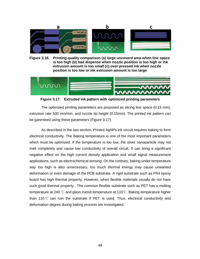
48
Figure 3.16. Printing quality comparison (a) large uncoverd area when line space is too high (b) bad dispense when nozzle position is too high or ink extrusion amount is too small (c) over pressed ink when nozzle position is too low or ink extrusion amount is too large
Figure 3.17. Extruded ink pattern with optimized printing parameters
The optimzied printing parameters are proposed as slicing line space (0.15 mm),
extrusion rate 500 mm/min, and nozzle tip height (0.15mm). The printed ink pattern can
be garenteed using these parameters (Figure 3.17).
As described in the last section. Printed AgNPs ink circuit requires baking to form
electrical conductivity. The Baking temperature is one of the most important parameters
which must be optimized. If the temperature is too low, the silver nanoparticle may not
melt completely and cause low conductivity of overall circuit. It can bring a significant
negative effect on the high current density application and small signal measurement
applications, such as electrochemical sensing. On the contrary, baking under temperature
way too high is also unnecessary, too much thermal energy may cause unwanted
deformation or even damage of the PCB substrate. A rigid substrate such as FR4 epoxy
board has high thermal property. However, when flexible materials usually do not have
such good thermal property. The common flexible substrate such as PET has a melting
temperature at 240 ℃ and glass transit temperature at 110℃. Baking temperature higher
than 110℃ can ruin the substrate if PET is used. Thus, electrical conductivity and
deformation degree during baking process are investigated.

49
Figure 3.18. Electrical resistivity measurement by four point probe method [108]. Reprinted with permission.
A four point probe method is the most common used method for measuring the
electrical conductivity/resistivity of thin depth (Figure 3.18). The four point probe contains
four thin collinearly placed tungsten wires probes which are made to contact the sample
under test. Current I is made to flow between the outer probes, and voltage V is measured
between the two inner probes, ideally without drawing any current. If the sample is of semi-
infinite volume and if the inter-probe spacings are s1= s2 = s3 = s, then it can be shown
that the resistivity of the semi-infinite volume is given by
𝑅 = 𝑘 (𝑉
𝐼) (3.1)
Where 𝑘 is the a geometric factor. In the case of a thin sheet, k = 4.53 [108].
However, this method requires four probe stations, which was not available in the lab.
Therefore, a alternative method was implemented. Two probe method is the simplest
method of measuring resistivity and is illustrated in Figure 3.19. In this method, voltage
drop V across the sample and current through the sample I are measured. Then the
resistivity is given as
𝑅 =𝑉𝐴
𝐼𝐿 (3.2)

50
Figure 3.19. Electrical resistivity measurement by two probe method [108]. Reprinted with permission.
where A is the cross sectional area of the specimen. In order to minimize the error,
seven identical samples (10mm× 3mm) were printed by V-one on PET substrate with a
thickness of 50 m. Each sample is baked under 30℃, 50℃, 70℃, 100℃, 130℃, 160℃,
and 190℃ for 1 hour (Figure 3.20a). Their resistivity was calculated according to the two
probe method. Each printed specimen was measured by the probe station inside of a
vacuum chamber (Figure 3.20b). According to data from figure 3.18, the optimized
temperature with 70℃ is lower than a glass transit temperature of PET (110℃). Thus,
annealing process does not cause unexpected curvature of the sensor substrate.
Figure 3.20. (left) Printed ink specimen on PET substrate with different baking temperatures (right) resistivity measurement setup using the probe station

51
Figure 3.21. Electrical resistivity of printed silver ink under different baking temperature
Figure 3.22. Micro images of printed AgNP ink before baking and after baking using optimized baking temperature

52
3.4. 3D Printed Flexible Electro-chemical Sensor
Several designs of sensor electrode were tested in term of mechanical durability
and space efficiency. The very first sensor was printed on FR4 substrate without
considering the physical connection between itself and potentiostat. As a result, printed
electrode pattern with conductive ink was fine, but soldering process a thin wire on the
electrode destroyed the printed electrode because of the high temperature of soldering
gun (Appendix A). Later, optimized electrode design adapted a feature of card edge
connector (Figure 3.19). In this way, the sensor can be inserted into a three-pin card edge
connector without the risk of damage. The final design of the proposed flexible lactate
sensor patch is shown in Figure 3.20 which contains two three-electrode electrochemical
sensors that include two individual working electrodes (WE, 2mm dia.), a sharing
reference electrode (RE, 4mm 0.5mm), and a sharing counter electrode (CE, 4mm
3mm). The electrodes are fabricated with AgNP ink on flexible PET substrate via a 3D-
printing process using AgNPs by using a 3D-printer from Voltera. In order to enhance the
printed electrodes' conductivity, a thermal annealing process is optimized as described in
section 3.3. The baking temperature was 70℃.
Figure 3.23. First sensor design with card edge connection feature (left) CAD deisgn (middle) printed electrodes on rigid FR4 board (right) printed electrodes on PET substrate

53
Figure 3.24. Final sensor design with card edge connection feature (left) CAD design (middle) printed electrodes on rigid FR4 board (right) printed electrodes on PET substrate
3.4.1. Formation of Working Electrode
Nafion has received substantial attention as electrolyte polymer in Chlor-alkali
electrolyzers replacing sodium amalgam or diaphragm cells and in proton exchange
membrane (PEM) fuel cells due to unique ionic selectivity, chemical resistance, excellent
thermal and mechanical stability. Perfluorosulfonic membrane Nafion was first developed
by Dupont de Nemours in 1962. Sulfonated fluoropolymer has a hydrophobic backbone
of polytetrafluoroethylene (PTFE) with side chains containing hydrophilic sulfonate ionic
group[109-110]. The chemical formula is:
Nafion is an artificial polymer well-known for its excellent biocompatibility and
perm-selectivity. According to work done by M.A. Abrar [22]. The negatively charged
Nafion shows its ability to eliminate anionic interferences such as ascorbic acid and nitrite.
However, a significant decrease in sensitivity has been observed both for sensors
incorporating Nafion as mixed with enzyme matrix and used as a separate layer on the
sensor surface. Thus an optimum concentration of the selective membrane needs to come
of age. Diluted Nafion solution with a concentration of 5% has been showed recently to
permit maximum hydrogen peroxide to pervade through while still effectively acting as an
impermeable membrane to block ascorbate.

54
Nafion was received as a 20 wt. % mixture of lower aliphatic alcohols and water.
It was dissolved in ethanol to prepare diluted (5% v/v) Nafion solution. To prepare the
Nafion selective membrane, 20 μL of the solution was drop cast on the electrode surface
and left it to dry for an hour.
Glutaraldehyde (GA) - as a cross-linking agent; was used to immobilize Lactate
Oxidase (LOD) in conjunction with Bovine Serum Albumin (BSA) as stabilizing reagent.
50 U of LOD was dissolved in 500 μL of Phosphate Buffer Saline (PBS) and was equally
separated into 25 aliquots; each containing 2 U of LOD. All aliquots were stored at -200C
A total mass of 6 mg of BSA was dissolved in 40 μL of PBS and stored at 40C. Prepared
BSA solution was mixed with 20 μL of LOD solution and stored at 40C. Glutaraldehyde
(GA) was diluted into 10% solution with DI water, and a 30 μL of diluted GA solution was
concocted with LOD/BSA mixture and 20 μL of LOD/BSA/GA of the solution was drop cast
on Nafion coated electrode surface. After waiting for 2 hours, the prepared sensor was
gently rinsed with PBS to get rid of excess GA.
Figure 3.25. Cross sectional structure of the working electrode with enzyme layer
3.4.2. Generation of Reference Electrode
One of the most common reference electrode used for electrochemical
measurements is silver/silver chloride (Ag/AgCl) electrode. These are quite stable, robust,
usable under a wide variety of conditions and cheap to fabricate. A most common
technique to chloridized silver is to electroplate it in a chloride containing the solution.
Electroplating of a silver wire could be achieved by placing it in a cell containing 0.1~1 M
HCl or KCl and applying about 0.5 mA/cm2 for 30 minutes. If chloridized in the absence
of light, the color should turn in to reddish dark brown or pale tan otherwise. Periodic
reversal of the polarity of the electrode while plating tends to yield a more stable reference

55
electrode. After washing with water, the color of the coating ranges from pink to shade of
plum.
An easy and inexpensive alternative method could be employed to soak silver in
hypochlorite solution that obviates the need for an electrochemical cell. Commercial
household bleach can be used in this regard. Ag/AgCl reference electrodes for the lactate
sensor were prepared by dunking 3D printed electrodes in 8.25% Clorox bleach for 30
second and then they were washed with DI water. The final fabricated lactate sensor can
be inserted into a 3-pin card edge connector (Figure 3.22).
Figure 3.26. (left) proposed printed lactate biosensor prototype with WE covered by the enzyme and chloridized RE (right) lactate biosensor connected with a 3-pin card edge connector
3.5. Design of 3D Printed Potentiostat
Numerous commercial instruments are available; unfortunately, commercial
potentiostats are expensive and operate with limited design information available to users
about their circuitry and behavior. Thus, most potentiostats impose significant constraints
on researchers who are developing new measurement techniques and application.
Benchtop potentiostat systems can perform numerous electrochemical analysis
techniques within a wide range of parameters including variations of signal output and
data interpretation. However, our initial potentiostat system design focus on performing
cyclic voltammetry and amperometry. As such, many costs were omitted by minimizing

56
system requirements and controls; these design parameters also allowed for minimization
of the device size.
To perform cyclic voltammetry, a voltage is applied to the working electrode,
momentarily held at an initial voltage, and linearly decreased until a vertex voltage is
reached. The voltage is then reversed and swept back towards the initial value.
Throughout this cycle, electron transfer occurs within the electrochemical cell; this current
is measured at the working electrode and recorded for analysis. This section discusses
how the potentiostat was designed to accomplish these tasks.
Figure 3.27. Block diagram of the potentiostat
3.5.1. Design and Fabrication of Potentiostat Circuits
The potentiostat circuit had endured several redesigns before a final design was
established. However, in every design, the potentiostat circuit must embed the necessary
components to execute electrochemical functionalities. The major tasks are voltammetric
for the potential sweep and current conversion for small signal acquisition. Meanwhile, to
assure the durability and reliability of physical implementation of 3D printing, its PCB
design has to be as lean as possible.

57
Figure 3.28. Detail schematic diagram of the proposed potentiostat system design
A single channel potentiostat based on a similar circuit architecture to the
CheapStat [109] is designed. The schematic diagram of the fabricated potentiostat circuit
and is shown in Figure 3.24. In order to study the electrochemical behavior of analytes,
careful control of the interfacial potential between WE and RE from an electrochemical
cell is essential to allow electrochemical current to be measured at a stable level during a
short period. In order to apply potential, RE with constant potential is required. A low-
power microcontroller (ATXMEGA32, Atmel) serves as the core for generation of
voltammetric excitations. In order to realize the electrochemical test function such as cyclic
voltammetry, the potentiostat has to generate a sweep potential in desired range and scan
rate in both forward and reverse directions. Thus, a comparison circuit with a bidirectional
switch in Figure 3.25 is connected to a digital-to-analog converter (DAC). It generates the
potential in a range from -1.65V to 1.65V across the WE and RE with a resolution of 0.8
mV. In the meantime, an operational amplifier (TLC2264ID, Texas Instrument) serves as
a current buffer due to its infinity high input impedance to limit any current that might flow
through RE. Therefore, the current is forced to flow between WE and CE. Thereby, RE
remains in proper polarity to keep the WE potential at a constant value with respect to the
RE.

58
Figure 3.29. Electrometer generator circuit
The lactate sensor output current is usually in the range of 10−6 μA. The common
approach of current measurement in voltammetric cells is the use of a trans-impedance
amplifier instead of an operational amplifier. A feedback resistor (R𝑓) is placed between
the inverting input and the output, while the non-inverting input is grounded. Fabricated
potentiostat design includes a transimpendace amplifier (OPA380, Texas Instrument),
because of its ultra-low input impedance and a high output impedance as shown in Figure
3.26. The converted voltage at the output is
𝑉𝑜𝑢𝑡𝑝𝑢𝑡 = 𝑉𝑟𝑒𝑓 + 𝐼𝑅𝑓 (3.3)
where R𝑓 is the gain in the feedback path. Thus, measurement ranges of electrochemical
currents are adjusted via onboard jumper as ±10 μA, ±50 μA, and ±100 μA with resolution
of 4.88 nA, 24 nA, and 48.8 nA respectively.
Figure 3.30. OPA380 trans-impedance amplifier i-v converter
A 2nd order Sallen-Key low pass filter is implemented to wipe out any noise signal
larger than 60 Hz, because of its high selectivity as shown in Figure 3.27. Also, the
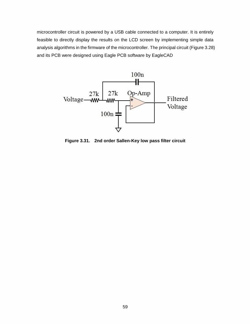
59
microcontroller circuit is powered by a USB cable connected to a computer. It is entirely
feasible to directly display the results on the LCD screen by implementing simple data
analysis algorithms in the firmware of the microcontroller. The principal circuit (Figure 3.28)
and its PCB were designed using Eagle PCB software by EagleCAD
Figure 3.31. 2nd order Sallen-Key low pass filter circuit

60
Figure 3.32. Schematic of potentiostat circuit design using Eagle PCB. Zoom in detail is in appendix C
Figure 3.33. (left)Test potentiostat PCB fabricated by the conventional method (right) Test setup for the conventional potentiostat

61
3.5.2. Development of Potentiostat Firmware
Two software programs were written to control the portable potentiostat: the
software used to program the microcontroller and the digital circuit, and the software used
to capture the output data and plot the results in real time. Appreciated to the open source
firm from 'CheapStat.' The microcontroller firmware was updated on the original
architecture in the AVR Studio 4 using C language. The c. project file must be converted
to hex file using WinAVR in order to burn the firmware into the MCU (Appendix C). The
full program is provided in Appendix D contains all code and comments in further detail.
An overall program is a state machine, which can switch the functions(CV or amperometry)
depending on user's input parameter. To execute electrochemical functionalities, it is
established with a counter and a while loop. Once the user has input an initial and peak
voltage, and the start button has been pushed, the counter begins counting until the initial
voltage (corresponding to a number between 0 and 255) is reached. At this moment, the
output of the counter is enabled. The counter continues to count down until the peak
voltage is reached and then begins to count upwards. Once the initial voltage is once
again achieved, the loop terminates. The second task is accomplished by a series of
analog reads and an averaging algorithm. The output of the ADC is read eight times per
step of the voltage sweep; the weighted average is computed for both the applied voltage
as well as the resulting current. The communication software, described in the following
section, retrieves these values and creates a plot in real time.
The graphical user interface (GUI) was programmed in JavaScript which is used
to upload data retrieved by a microcontroller to an Excel spreadsheet in real time. The
GUI was implemented to allow the user to see what values are being selected by the
potentiometers, as well as to initiate and terminate the connection with the device. The
voltage applied to the electrochemical cell, as well as the current generated at the working
electrode, were updated to an Excel spreadsheet and plotted in real time. The user may
also clear the data from the spreadsheet at any time.

62
3.6. 3D Printed Potentiostat on Epoxy Board
3.6.1. Design Optimization of Potentiostat PCB
The design process needs to follow previous circuit requirements to guarantee
electrochemical functionality. Although the use of conventional PCB CAD design software
for layout and routing of 3D-printed electronic devices is possible when the flat-board
design is involved, the software still lacks the support on 3D-printing feature and design
routine checking. Therefore, multiple 3D-printing routings and pad optimizations are
manually done. Firstly, a 3D-PCB shall perform excellent electrical conductivity in the
printed circuit trace pattern to avoid disturbance of electrical signals from resistance loss.
Secondly, the resolution of printed traces and clearances need to meet the requirements
for modern electronic packages. Thirdly, minimizing the physical connection on board with
possible force applied (e.g. jumper pins, cable socket) is critical because unlike soldering
ICs on foiled copper, it is much weaker when soldering ICs on the silver pad. Falling off
any ICs from PCB may cause system failure.
In PCB design, the term of design rule is a categorization of parameters based on
capabilities of the equipment and the overall process. Design rule checking (DRC) makes
sure the physical PCB layout of a particular chip layout satisfies design rules parameters
including minimum trace width, minimum trace spacing, drilling/via diameter. The general
design rule limitations of conventional PCB technology are trace width of 6 mil (0.15 mm),
trace space of 6 mil, and minimum finished drill of 12 mil (0.3 mm). As mentioned in
section 3.1. The printhead nozzle diameter is 200 um (8mil). The pattern resolution of the
printing system is 150 m (6mil) [110]. The minimum pin-to-to pitch which printing system
can achieve is 500um. Both parameters can satisfy conventional PCB design rules and
modern IC packaging.

63
3.6.2. Prototyping of 3D Printed Potentiostat
Several versions 3D-PCB layout were designed. In the early attempts, SMD
components and DIP components were separated on two 3D-PCBs with connection by
jumper cable (Figure 3.32). The purpose was to reduce the density of ICs and traces on
the board, thereby reduced the possibility of error and increased the printing quality by V-
ONE. Moreover, the LCD screen is sensitive to high temperature, which cannot be
soldered using reflow process.
Figure 3.34. Early potentiostat prototype on separated 3D-PCBs
After the printing process and optimal printing parameter were secured, more
integrated 3D-PCB was designed (Figure 3.33), both SMD component and DIP
component were on the same board. Two card edge connection pad (3-pin and 4-pin)
were designed to replace dip connection for programmer and sensor. Figure 3.33 showed
the latest PCB layout in EagleCAD and proposed connection feature between 3D-PCB
potentiostat and sensor. The final 3D-PCB was printed using parameters of 0.15 mm line
spacing, 150 um nozzle height, and 50 extrusion amount. After verifying the conductivity
of each traces. Solder paste was dispensed on the component pads, and all the SMD
components were placed onto along with a DIP socket. In the way, entire 3D-PCB can be
implemented in the reflow process without damaging any components. Finally, an LCD
screen was plugged into the dip sockets (Figure 3.34). The whole fabrication process is
no more than 8 hours.

64
Figure 3.35. (a) latest PCB layout in EagleCAD (b) proposed connection feature between 3D-PCB potentiostat and sensor
Figure 3.36. The final 3D-PCB p4otentiostat with SMD components and DIP sockets

65
Chapter 4. Characterization of 3D Printed Electrochemical System
4.1. Characterization of 3D printed Lactate Sensor
Proposed 3D-printed lactate sensor's electrochemical behavior is verified with
Cyclic Voltammetry (CV) test performed on a commercial electrochemical analyzer (CHI
1205B, CH Instruments Inc.) before using the 3D-printed potentiostat. Cyclic voltammetry
is a typical voltammetric technique where the linear potential ramp is applied between
electrodes. Redox current pattern typically shows a duck shape. Lactate solutions are
prepared in PBS (pH = 7.0) with 5 mM, 10 mM, and 15 mM concentration. 20 L-lactate
solutions were dropped evenly via micropipette onto the sensor test area with a scan rate
of 100 mV/s to the WE versus the RE. The generated currents in the measurement range
from -2 V to 2 V is analyzed. The current-potential data on a computer is obtained. Figure
4.1(a) shows a group of typical cyclic voltammograms at different lactate concentrations.
The graphs of the cyclic voltammograms reveal a typical reversible redox reaction.
Receptively, cathodic peak current ((I𝑝𝑐) and anodic peak current (I𝑝𝑎) are located at 0.25
V and -0.5 V. Therefore, the operating potential of the lactate sensor is selected according
to the CV results. The operational potential is 0.25 V for all the subsequent since the
oxidation peak is found at 0.25V.
The amperometric response of the biosensor upon addition of lactate with different
concentrations is presented. Current response rises linearly as the concentration
increases from 0 to 15 mM (Figure 4.2a). Sensor response reaches to 90 % of the constant
value within 60 seconds. Moreover, sensor's durability and stability are also important
properties. The amperometric response is investigated on the same lactate sensor after
24 hours. The respond current keep in same order of a few tens of A (Dash curves in
Figure 4.2b). Therefore, the proposed lactate sensor can readily implement with a 3D-
printed potentiostat.

66
Figure 4.1. Lactate biosensor charetericaztion test results: (a) cyclic voltammetry curve using 5,10,and 15mM lactate solution. (b) Amperometric measurements in new condition and in 24 hours.
4.2. Cyclic Voltammetry for Redox Analysis
In order to verify the 3D-printed potentiostat system, a comparative test was
investigated depending on different scan rates using the fabricated 3D-printed potentiostat
(Figure 4.2). CV test was executed with 15 mM lactate which the potential value was
sweeping from -1.6 V to 1.6 V with five scan rates (50 mV/s, 100 mV/s, 200 mV/s, 300
mV/s, and 400 mV/s). In cyclic voltametry, the Randle-Seycik equation indicates the
effects of concentrations of electroactive species and scan rate on the peak current. When
the concentration of lactate is constant, the redox peak current in a cyclic voltammetry is

67
proportional to the square roots of scan rate. Higher CV scan rates give rise to higher
redox current. The analyzed result shows that the relationship between the scan rate and
peak current fits the Randles-Sevcik equation.
Figure 4.2. (left) cyclic voltammograms measurement of 15 mM Lactic Acid solution at different scan rates from 50mV/s to 400mV/s, (right) linear relation between absolute value of anodic current peak and square root of scan rate
According to the results, it appears that the total current increases with increasing
scan rate. This can be explained by considering the size of the diffusion layer and the time
taken to record the scan. The Cyclic voltammogram will take a shorter time to record as
the scan rate is increased. Therefore the size of the diffusion layer above the electrode
surface will be different depending upon the voltage scan rate used. In a slow voltage
scan, the diffusion layer will grow much further from the electrode in comparison to a fast
scan. Consequently, the reactant flux to the electrode surface is smaller at slow scan rates
than it is at faster scan rates. As the current is proportional to the flux towards the
electrode, the magnitude of the current will be lower at slow scan rates and higher at high
rates. The quantitative detail of this behavior is described as Randles-Sevcik equation. In
this equation, the peak current 𝑖𝑝 can be predicted using equation (2.12). Moreover, it is
clear that the peak occurs at the same voltage and this is a characteristic of electrode
reactions which have rapid electron transfer kinetics.
Furthermore, in order to characterize the 3D-PCB potentiostat electronics
performance. CV and amperometric tests were performed using the 3D-PCB potentiostat
and the conventional PCB potentiostats which mentioned in section 3.31 under same
conditions. The CV scan rate is 100 mV/s, and the potential sweep range is from -1.6 V to
16.V. The lactate solutions are measured in 5 mM, 10 mM, and 15 mM concentration.

68
Figure 4.3a shows the CV test curve from conventional PCB potentiostat. Moreover,
Figure 4.3b shows the CV from 3D-PCB potentiostat. Both CV test curves show a typical
duck shape with significant reduction peak at the potential of -0.5 V. Nevertheless; it is
evident that CV curves that from 3D-printed potentiostat have larger noise oscillations than
the potentiostat made by conventional PCB. Overall, the CV data with two potentiostats:
conventional PCB and 3D-printed PCB show very similar regarding peak currents, peak
potentials, and current densities characteristics expect the signal to noise.
Figure 4.3. Cyclic voltammetry measurements of lactic acid at 100mV/s scan rate via (a) proposed potentiostat design using conventional PCB fabrication method (b) proposed potentiostat design using 3D printing method

69
4.3. Amperometric i-t curve and Calibration
Amperometric i-t curve measures the current at a fixed working electrode potential,
and the resulting current from the electrode is monitored as a function of time. This current-
time curve represents the change in the concentration gradient. As time goes, the reactant
depletes at the working electrode surface, and the slope of the response decreases as
well. A constant 0.25 V potential is applied between WE and RE in the amperometric
response test based on previous CV results. All In vitro experiments were carried out by
drop casting and bearing off 50 μL of the solution with different concentrations on the
sensor each time. The amperometric response by using conventional PCB (Figure 4.5a)
and 3D-PCB potentiostat (Figure 4.5b) are presented respectively. Current response rises
linearly as the lactate concentration increases from 0 to 20 mM in both potentiostat
devices. Current response rises as the concentration increases from 0 mM to 25 mM.
Sensor response reaches to 90% of its final steady value within 60 seconds (response
time).
Figure 4.4. (a) test setup for 3D-PCB potentiostat prototype with lactate sensor (b) zoom in the image of drop cast of lactate acid solution on the sensor

70
Figure 4.5. Amperometric measurements within lactate solutions. (a) proposed potentiostat design using conventional PCB fabrication method (b) proposed potentiostat design using a 3D printing method
Obviously, the measured currents from 3D PCB potentiostat are higher than the
current from potentiostat on conventional PCB, as well as the signal noise. There are two
reasons: Firstly, sintered AgNP's electrical conductivity is lower than coppers'. Therefore,
there is more resistivity lost on the 3D PCB potentiostat along the circuit trace. When
measuring the same amount of driving current, the converted voltage is larger due to the
large resistance. Secondly, unlike the copper pad which IC components can be soldered
homogeneously, AgNP pad has poorer solder ability. Poorly soldered structures between
IC component pins and 3D PCB pad increase the resistivity lost significantly as well.
Therefore, minimizing the resistivity lost along the 3D PCB trace and solder structure can
deliver better measurement performance.

71
Chapter 5. Conclusion and Future Work
5.1. Conclusion
The primary purpose of this work was to investigate and demonstrate the use of
3D printing technology to fabricate an electrochemical device combined with 3D printed
potentiostat PCB, along with a flexible lactate biosensor for noninvasive continuous lactate
measurement.
3D printing technology integration
The main techniques of 3D printing were studied, each advance and limitations in
the different fabricating processes were discussed. Direct Ink Writing (DIW) was selected
as the best 3D printing method to fabricate PCB and sensor. A novel 3D ink printer(V-
ONE) was utilized as the PCB printing platform. A pure additive manufacture procedure
demonstrates the ability to print single layer double sides PCB by dispensing a high
viscosity AgNP ink. Printing parameters were investigated. Thus this 3D PCB printing
platform can generate PCBs which meet most design standard compared with traditional
PCBs. The proposed PCB 3D printing method by printing silver ink to generate circuit
significantly accelerate the fabrication process of conventional electronic PCB. The lead
time for electronics prototyping can be reduced to hours.
Development of Potentiostat
A functional potentiostat was developed base on 'CheapStat' open source
structure. The circuit was re-designed with the addition of trans-impedance amplifier as
the electrochemical current converter for better sensitivity and accuracy. PCB layout was
simplified as lean as possible with only necessary ICs for CV and amperometry functions.
Two potentiostats were fabricated using both conventional method and proposed 3D
printing method for the purpose of comparison.
3D printing of sensor electrode
72
Sensor electrode was fabricated using 3D printing technique. The steps followed
towards the development of the concept and fabrication of flexible sensing platform for
lactate monitoring. All three electrodes were fabricated on PET substrate using silver
nanoparticle.
Demonstration of 3D printed electrochemical system
A fully 3D printed sensor and sensor module system with printed PCB-based
potentiostat has been demonstrated. The printed lactate biosensor shows a linear
amperometric response linear dependence with lactate concentration of 1~20 mM/L
during the in-vitro experiments. Integrated with the printed lactate biosensor, cyclic
voltammetry and amperometric are demonstrated. Experimental results show that the
performance of the 3D-PCB based potentiostat is reliable as that of conventionally
fabricated PCB.
5.2. Future Works
This work was an attempt as to demonstrate the possibility of using 3D printing
technology to fabricate PCB system for electrochemical applications. Future work aims to
improve AgNP conduct ink material’s electrical and mechanical property. Both analog and
high frequency digital applications can be achieved when the resistivity reduction is
minimized. Maximizing printing speed without compromising print quality will be a problem
of interest, and it will involve developing an optimal printing sequence to minimize printing
artifacts. In addition, usage of computational methods can optimize the fabrication
accuracy and 3D PCB success rate. For example, developing an automatic drilling
mechanism will improve the 3D printed PCB quality and reduce chance of fail. Flexible
electronics circuit printing is another area of interest; the conductive ink was demonstrated
using low sintering temperature. Thereby complex circuit could be printed not only on rigid
board but also on a flexible substrate with multi-layer features.

73
References
[1] Hull, Charles W. "Apparatus for production of three-dimensional objects by stereolithography." U.S. Patent No. 4,575,330. 11 Mar. 1986.
[2] Singh, Rupinder. "Three dimensional printing for casting applications: A state of art review and future perspectives." Advanced Materials Research. Vol. 83. Trans Tech Publications, 2010.
[3] Lewis, Jennifer A., et al. "Direct ink writing of three‐dimensional ceramic structures." Journal of the American Ceramic Society 89.12 (2006): 3599-3609.
[4] Barnatt, Christopher. 3D printing: the next industrial revolution. ExplainingTheFuture. com, 2013.
[5] Gooding, J. Justin. "Nanostructuring electrodes with carbon nanotubes: A review on electrochemistry and applications for sensing." Electrochimica Acta50.15 (2005): 3049-3060.
[6] Robertson, Christopher T. Printed circuit board designer's reference: basics. Prentice Hall Professional, 2004.
[7] Gross, Bethany C., et al. "Evaluation of 3D printing and its potential impact on biotechnology and the chemical sciences." (2014): 3240-3253.
[8] MacDonald, Eric, and Ryan Wicker. "Multiprocess 3D printing for increasing component functionality." Science 353.6307 (2016): aaf2093.
[9] Dimension, N. (2017). 3D PCB Printer Readiness Survey: The Results!. [online] Nano-di.com. Available at: http://www.nano-di.com/blog/printer-readiness-survey-results-april-2016 [Accessed 7 Aug. 2017].
[10] Israel : Survey Uncovers High Costs, Risks Associated with Prototyping PCBs Off-Site.” MENA Report, Albawaba (London) Ltd., Apr. 2016.
[11] EETimes. (2017). When 3D Printing Meets PCBs | EE Times. [online] Available at: http://www.eetimes.com/author.asp?doc_id=1329449 [Accessed 7 Aug. 2017].
[12] Vadgama, P., et al. "The glucose enzyme electrode: is simple peroxide detection at a needle sensor acceptable?." Hormone and metabolic research. Supplement series 20 (1988): 20-22
[13] Parolo, Claudio, and Arben Merkoçi. "based nanobiosensors for diagnostics." Chemical Society Reviews 42.2 (2013): 450-457.

74
[14] Li, Huaqing, et al. "Multi-channel electrochemical detection system based on LabVIEW." Information Acquisition, 2004. Proceedings. International Conference on. IEEE, 2004.
[15] Gao, Wei, et al. "Fully integrated wearable sensor arrays for multiplexed in situ perspiration analysis." Nature 529.7587 (2016): 509-514.
[16] Zhao, Chen, Martin M. Thuo, and Xinyu Liu. "A microfluidic paper-based electrochemical biosensor array for multiplexed detection of metabolic biomarkers." Science and technology of advanced materials 14.5 (2013): 054402.
[17] Imani, Somayeh, et al. "A wearable chemical–electrophysiological hybrid biosensing system for real-time health and fitness monitoring." Nature communications 7 (2016): ncomms11650.
[18] Sanghavi, Bankim J., et al. "Nanomaterial-based electrochemical sensing of neurological drugs and neurotransmitters." Microchimica Acta 182.1-2 (2015): 1-41.
[19] Stević, Zoran, Zoran Andjelković, and Dejan Antić. "A New PC and LabVIEW package based system for electrochemical investigations." Sensors 8.3 (2008): 1819-1831.
[20] Cruz, Andres Felipe Diaz, et al. "A low-cost miniaturized potentiostat for point-of-care diagnosis." Biosensors and Bioelectronics 62 (2014): 249-254.
[21] MacDonald, Eric, and Ryan Wicker. "Multiprocess 3D printing for increasing component functionality." Science 353.6307 (2016): aaf2093.
[22] Abrar, Md Abu, et al. "Bendable Electro-chemical Lactate Sensor Printed with Silver Nano-particles." Scientific reports 6 (2016): 30565.
[23] Wang, Joseph. Analytical electrochemistry. John Wiley & Sons, 2006.pp. 29-42, 67-85.
[24] Chem.libretexts.org. (2016). [online] Available at: http://chem.libretexts.org/Textbook_Maps/Analytical_Chemistry_Textbook_Maps/Map%3A_Analytical_Chemistry_2.0_(Harvey)
[25] D. C. Harris, "Quantitative Chemical Analysis," pp. 270-320, 348-372, 2007.
[26] Zoski, Cynthia G., ed. Handbook of electrochemistry. Elsevier, 2006.
[27] Community.asdlib.org. (2017). Reference Electrodes | Image and Video Exchange Forum. [online] Available at: http://community.asdlib.org/imageandvideoexchangeforum/2013/07/31/reference-electrodes [Accessed 8 Aug. 2017].

75
[28] Wang, Joseph. Analytical electrochemistry. John Wiley & Sons, 2006. 115-136, 165-185, 2006.
[29] Harvey, David. Modern analytical chemistry. Vol. 381. New York: McGraw-Hill, 2000.
[30] Cottrell, F. G. "Residual current in galvanic polarization regarded as a diffusion problem." Z. phys. Chem 42 (1903): 385-431.
[31] Clark, Leland C., and Champ Lyons. "Electrode systems for continuous monitoring in cardiovascular surgery." Annals of the New York Academy of sciences 102.1 (1962): 29-45.
[32] Mabeck, Jeffrey T., and George G. Malliaras. "Chemical and biological sensors based on organic thin-film transistors." Analytical and bioanalytical chemistry 384.2 (2006): 343-353.
[33] Baughman, Ray H., Anvar A. Zakhidov, and Walt A. De Heer. "Carbon nanotubes--the route toward applications." science 297.5582 (2002): 787-792.
[34] Evans, Dennis H., et al. "Cyclic voltammetry." (1983): 290.
[35] Wang, Joseph. "Electrochemical glucose biosensors." Chemical reviews 108.2 (2008): 814-825.
[36] YouTube. (2017). A level. S.5 Immobilisation of enzymes Ms Cooper. [online] Available at: https://www.youtube.com/watch?v=f163ohXmKEI [Accessed 8 Aug. 2017].
[37] Khan, M. A., A. A. Al-Jalal, and I. A. Bakhtiari. "'Decoking'of a'coked'zeolite catalyst in a glow discharge." Analytical and bioanalytical chemistry 377.1 (2003): 89-96.
[38] Nunes, Lázaro Alessandro Soares, and Denise Vaz de Macedo. "Saliva as a diagnostic fluid in sports medicine: potential and limitations." Jornal Brasileiro de Patologia e Medicina Laboratorial 49.4 (2013): 247-255.
[39] MacLean, Dave A., Jens Bangsbo, and Bengt Saltin. "Muscle interstitial glucose and lactate levels during dynamic exercise in humans determined by microdialysis." Journal of Applied Physiology 87.4 (1999): 1483-1490.
[40] Thomas, Nicole, Ilkka Lähdesmäki, and Babak A. Parviz. "A contact lens with an integrated lactate sensor." Sensors and Actuators B: Chemical 162.1 (2012): 128-134.
[41] Marek, E. M., et al. "Measurements of lactate in exhaled breath condensate at rest and after maximal exercise in young and healthy subjects." Journal of breath research 4.1 (2010): 017105.

76
[42] Biagi, Simona, et al. "Simultaneous determination of lactate and pyruvate in human sweat using reversed‐phase high‐performance liquid chromatography: a noninvasive approach." Biomedical Chromatography26.11 (2012): 1408-1415.
[43] Derbyshire, Philip J., et al. "Lactate in human sweat: a critical review of research to the present day." The Journal of Physiological Sciences 62.6 (2012): 429-440.
[44] Coyle, Shirley, et al. "On-body chemical sensors for monitoring sweat." Wearable and autonomous biomedical devices and systems for smart environment. Springer Berlin Heidelberg, 2010. 177-193.
[45] Kreyden, Oliver P., and E. Paul Scheidegger. "Anatomy of the sweat glands, pharmacology of botulinum toxin, and distinctive syndromes associated with hyperhidrosis." Clinics in dermatology 22.1 (2004): 40-44.
[46] Stefaniak, Aleksandr B., and Christopher J. Harvey. "Dissolution of materials in artificial skin surface film liquids." Toxicology in Vitro 20.8 (2006): 1265-1283.
[47] Harvey, Christopher J., Ryan F. LeBouf, and Aleksandr B. Stefaniak. "Formulation and stability of a novel artificial human sweat under conditions of storage and use." Toxicology in Vitro 24.6 (2010): 1790-1796.
[48] Sato, Kenzo, and Richard L. Dobson. "Glucose metabolism of the isolated eccrine sweat gland: II. The relation between glucose metabolism and sodium transport." Journal of Clinical Investigation 52.9 (1973): 2166.
[49] Green, J. M., et al. "Sweat lactate response between males with high and low aerobic fitness." European journal of applied physiology 91.1 (2004): 1-6.
[50] Romero, Marcelo Ricardo, et al. "Amperometric biosensor for direct blood lactate detection." Analytical chemistry 82.13 (2010): 5568-5572.
[51] Ambrosi, Adriano, and Martin Pumera. "3D-printing technologies for electrochemical applications." Chemical Society Reviews 45.10 (2016): 2740-2755.
[52] Crump, S. Scott. "Apparatus and method for creating three-dimensional objects." U.S. Patent No. 5,121,329. 9 Jun. 1992.
[53] Wegst, Ulrike GK, et al. "Bioinspired structural materials." Nature materials14.1 (2015): 23-36.
[54] Zhu, Cheng, et al. "Highly compressible 3D periodic graphene aerogel microlattices." Nature communications 6 (2015): 6962.
[55] Hull, Charles W. "Apparatus for production of three-dimensional objects by stereolithography." U.S. Patent No. 4,575,330. 11 Mar. 1986.

77
[56] Bogue, Robert. "3D printing: the dawn of a new era in manufacturing?." Assembly Automation 33.4 (2013): 307-311.
[57] He, Yong, et al. "Developments of 3D printing microfluidics and applications in chemistry and biology: a review." Electroanalysis 28.8 (2016): 1658-1678.
[58] Choi, Jae-Won, et al. "Fabrication of 3D biocompatible/biodegradable micro-scaffolds using dynamic mask projection microstereolithography." Journal of Materials Processing Technology 209.15 (2009): 5494-5503.
[59] Feygin, Michael. "Apparatus and method for forming an integral object from laminations." U.S. Patent No. 4,752,352. 21 Jun. 1988.
[60] Rosen, David, and Lee Weiss. "Layered manufacturing: current status and future trends." Ann, Arbor 1001 (2001): 48109.
[61] Deckard, Carl R. "Method and apparatus for producing parts by selective sintering." U.S. Patent No. 4,863,538. 5 Sep. 1989.
[62] Ko, Seung H., et al. "All-inkjet-printed flexible electronics fabrication on a polymer substrate by low-temperature high-resolution selective laser sintering of metal nanoparticles." Nanotechnology 18.34 (2007): 345202.
[63] Gothait, Hanan. "Apparatus and method for three dimensional model printing." U.S. Patent No. 6,259,962. 10 Jul. 2001..
[64] Muth, Joseph T., et al. "Embedded 3D printing of strain sensors within highly stretchable elastomers." Advanced Materials 26.36 (2014): 6307-6312.
[65] Park, Yong-Lae, Bor-Rong Chen, and Robert J. Wood. "Design and fabrication of soft artificial skin using embedded microchannels and liquid conductors." IEEE Sensors Journal 12.8 (2012): 2711-2718.
[66] Frutiger, Andreas, et al. "Capacitive soft strain sensors via multicore–shell fiber printing." Advanced Materials 27.15 (2015): 2440-2446.
[67] Saari, Matt, et al. "Fabrication and Analysis of a Composite 3D Printed Capacitive Force Sensor." 3D Printing and Additive Manufacturing 3.3 (2016): 136-141
[68] Suaste-Gómez, Ernesto, et al. "Developing an ear prosthesis fabricated in polyvinylidene fluoride by a 3D printer with sensory intrinsic properties of pressure and temperature." Sensors 16.3 (2016): 332.
[69] Lin, Ying-Kai, et al. "Using Three-Dimensional Printing Technology to Produce a Novel Optical Fiber Bragg Grating Pressure Sensor." Sens. Mater28 (2016): 389-394.

78
[70] Rivadeneyra, Almudena, et al. "Improved manufacturing process for printed cantilevers by using water removable sacrificial substrate." Sensors and Actuators A: Physical 235 (2015): 171-181.
[71] Macdonald, Eric, et al. "3D printing for the rapid prototyping of structural electronics." IEEE Access 2 (2014): 234-242.
[72] Krachunov, Sammy, and Alexander J. Casson. "3D Printed Dry EEG Electrodes." Sensors 16.10 (2016): 1635.
[73] Cho, Sung-Joon, et al. "3D printed multi-channel EEG sensors for zebrafish." SENSORS, 2015 IEEE. IEEE, 2015.
[74] Adams, Jacob J., et al. "Conformal printing of electrically small antennas on three‐dimensional surfaces." Advanced Materials 23.11 (2011): 1335-1340.
[75] Nassar, I., H. Tsang, and T. Weller. "3D printed wideband harmonic transceiver for embedded passive wireless monitoring." Electronics Letters50.22 (2014): 1609-1611.
[76] Nassar, Ibrahim T., et al. "A High-Efficiency, Miniaturized Sensor Node With 3-D Machined-Substrate Antennas for Embedded Wireless Monitoring." IEEE Sensors Journal 15.9 (2015): 5036-5044.
[77] Lopez, Aida Garcia, Rohit Chandra, and Anders J. Johansson. "Optimization and fabrication by 3D printing of a volcano smoke antenna for UWB applications." Antennas and Propagation (EuCAP), 2013 7th European Conference on. IEEE, 2013.
[78] Mandon, Céline A., Loïc J. Blum, and Christophe A. Marquette. "Adding biomolecular recognition capability to 3D printed objects." Analytical chemistry 88.21 (2016): 10767-10772.
[79] Lind, Johan U., et al. "Instrumented cardiac microphysiological devices via multimaterial three-dimensional printing." Nature materials 16.3 (2017): 303-308.
[80] Sauerbrunn, Elizabeth, et al. "Thermal imaging using polymer nanocomposite temperature sensors." physica status solidi (a) 212.10 (2015): 2239-2245.
[81] Wickberg, Andreas, et al. "Three-dimensional micro-printing of temperature sensors based on up-conversion luminescence." Applied Physics Letters106.13 (2015): 133103.
[82] Li, Bo, et al. "Inkjet printed chemical sensor array based on polythiophene conductive polymers." Sensors and Actuators B: Chemical 123.2 (2007): 651-660.

79
[83] Kulkarni, Milind V., et al. "Ink-jet printed conducting polyaniline based flexible humidity sensor." Sensors and Actuators B: Chemical 178 (2013): 140-143.
[84] Song, Edward, et al. "Inkjet printing of conductive polymer nanowire network on flexible substrates and its application in chemical sensing." Microelectronic Engineering 145 (2015): 143-148.
[85] Naydenova, Izabela, et al. "Hybrid sensors fabricated by inkjet printing and holographic patterning." Chemistry of Materials 27.17 (2015): 6097-6101.
[86] Chen, Pochiang, et al. "Inkjet printing of single-walled carbon nanotube/RuO 2 nanowire supercapacitors on cloth fabrics and flexible substrates." Nano Research 3.8 (2010): 594-603.
[87] Yang, Li, et al. "A novel conformal RFID-enabled module utilizing inkjet-printed antennas and carbon nanotubes for gas-detection applications." IEEE Antennas and Wireless Propagation Letters 8 (2009): 653-656.
[88] Kim, Jiseok, and Woo Soo Kim. "Stretching silver: Printed metallic nano inks in stretchable conductor applications." IEEE Nanotechnology Magazine 8.4 (2014): 6-13.
[89] Macdonald, Eric, et al. "3D printing for the rapid prototyping of structural electronics." IEEE Access 2 (2014): 234-242.
[90] Franke, Jörg, ed. Three-Dimensional Molded Interconnect Devices (3D-MID): Materials, Manufacturing, Assembly and Applications for Injection Molded Circuit Carriers. Carl Hanser Verlag GmbH Co KG, 2014.
[91] Palmer, J. A., P. Yang, and D. W. Davis. Rapid prototyping of high density circuitry. Society of Manufacturing Engineers, 2000.
[92] Medina, Frank, et al. "Hybrid manufacturing: integrating direct-write and stereolithography." Proceedings of the 2005 solid freeform fabrication (2005): 129-143.
[93] Navarrete, Misael, et al. Integrated layered manufacturing of a novel wireless motion sensor system with GPS. TEXAS UNIV AT EL PASO WM KECK CENTER FOR 3D INNOVATION, 2007.
[94] Lopes, Amit, et al. "Expanding rapid prototyping for electronic systems integration of arbitrary form." 17th Annual Solid Freeform Fabrication Symposium, University of Texas at Austin, Austin, TX, Aug. 2006.
[95] Zhou, Nanjia, et al. "Gigahertz Electromagnetic Structures via Direct Ink Writing for Radio‐Frequency Oscillator and Transmitter Applications." Advanced Materials 29.15 (2017).

80
[96] Siggard, Erik J., et al. "Structurally embedded electrical systems using ultrasonic consolidation (UC)." Proceedings of the 17th solid freeform fabrication symposium. 2006.
[97] Nair, V., et al. "3D stacked embedded component system-in-package for wearable electronic devices." Radio and Wireless Symposium (RWS), 2017 IEEE. IEEE, 2017.
[98] Espalin, David, et al. "3D Printing multifunctionality: structures with electronics." The International Journal of Advanced Manufacturing Technology 72.5-8 (2014): 963-978.
[99] Olivas, Richard, et al. "Structural electronics through additive manufacturing and micro-dispensing." International Symposium on Microelectronics. Vol. 2010. No. 1. International Microelectronics Assembly and Packaging Society, 2010.
[100] Munakata, Riki. "Cubesat design specification rev. 12." The CubeSat Program, California Polytechnic State University 1 (2009).
[101] Boschetto, A., V. Giordano, and F. Veniali. "Surface roughness prediction in fused deposition modelling by neural networks." International Journal of Advanced Manufacturing Technology 67 (2013).
[102] Malone, Evan, and Hod Lipson. "Freeform fabrication of ionomeric polymer-metal composite actuators." Rapid Prototyping Journal 12.5 (2006): 244-253..
[103] Malone, Evan, Megan Berry, and Hod Lipson. "Freeform fabrication and characterization of Zn-air batteries." Rapid Prototyping Journal 14.3 (2008): 128-140.
[104] Janaki Ram, G. D., et al. "Use of ultrasonic consolidation for fabrication of multi-material structures." Rapid Prototyping Journal 13.4 (2007): 226-235.
[105] Park, Jae Sung, Mohamad Rezaei, and Woo Soo Kim. "Sustained Percolation in Stretched Silver Nanowire Networks for Stretchable Inter‐Connection Applications." Advanced Engineering Materials 16.7 (2014): 905-908.
[106] Stratasys.com. (2017). Smart Parts: Additive Manufacturing for Integrated Electro-mechanical Devices | Stratasys. [online] Available at: http://www.stratasys.com/resources/webinars/smart-parts.aspx [Accessed 8 Aug. 2017].
[107] Paulsen, Jason A., et al. "Printing conformal electronics on 3D structures with Aerosol Jet technology." Future of Instrumentation International Workshop (FIIW), 2012. IEEE, 2012.

81
[108] Singh, Yadunath. "Electrical resistivity measurements: a review." International journal of modern physics: Conference series. Vol. 22. World Scientific Publishing Company, 2013.
[109] Rowe, Aaron A., et al. "CheapStat: an open-source,“Do-It-Yourself” potentiostat for analytical and educational applications." PloS one 6.9 (2011): e23783.
[110] Robertson, Christopher T. Printed circuit board designer's reference: basics. Prentice Hall Professional, 2004.

82
Appendix A. Early electrodes design setup
First attempt of printing electrode on epoxy board without using card edge connection
design. Thin copper wires were manually soldered on printed electrodes. The high
temperature from solder gun damaged most electrodes

83
Appendix B. Programming Setup
To program the AVR microcontroller, original source file of C was converted to a
hex file using WinAVR. WinAVR is a suite of executable, open source software
development tools for the Atmel AVR series of RISC microprocessors hosted on the
Windows platform. It includes the GNU GCC compiler for C and C++. This hex is the
firmware code, in order to burn the firmware into the MCU, a AVR mkII programmer was
connected between laptop and the MCU using DPI mode. The connection is shown in
bottom figure. Pin 33,34,8,38 on the MCU was PDI_DATA,PDI_CLK,VCC, and GND
respectively.

84
Appendix C. Potentiostat Circuit Design Detail

85

86
Appendix D. Microcontroller code
#define F_CPU 2000000UL //CPU frequency #define TIMER TCC0 //timer to use #define DAC_CONINTVAL DAC_CONINTVAL_1CLK_gc //DAC settings #define DAC_REFRESH DAC_REFRESH_16CLK_gc #define ADC_PRESCALER ADC_PRESCALER_DIV8_gc //ADC sampling speed #define ADC_OFSET 0 #define EEPROM_SIZE 1024 //in bytes #define PROFILES_LENGTH 11 //max number of profiles, limited by memory #define SWV_BUFFER_SIZE 16 //must be <=16 #define SWV_MAX_DATAPOINTS 1000 #define CV_BUFFER_SIZE 16 //must be <=16 #define CV_MAX_DATAPOINTS 1500 #define LSV_BUFFER_SIZE 16 //must be <=16 #define LSV_MAX_DATAPOINTS 1500 #define CA_MAX_DATAPOINTS 1500 #define ACV_POINTSPERCYCLE 50 //#define DEBUG //#define DUBUGSIZE //#define DEBUG_INDEX_STOP 1000 //user interface #define SWV 0 #define CV 1 #define ACV 2 #define LSV 3 #define CONSTVOLT 4 #define CA 5 #define PROFILE_SEL 0 #define PROFILE_OPT 1 #define PROFILE_TEST 2 #define PROFILE_EDIT 3 #define PROFILE_RESULTS 4 #define EDIT_NOSEL 0 #define EDIT_SEL 1 #define OPT_START 0 #define OPT_EDIT 1 #define RANGE_10UA 1 #define NGE_50UA 2 #define UP 0 #define LEFT 1 #define RIGHT 2 #define DOWN 3 #define INVALID 4 #define bit_get(p,m) ((p) & (m)) //structure to store the profile - 29 bytes typedef struct { char name[15]; uint8_t type; int16_t op1;

87
int16_t op2; int16_t op3; int16_t op4 int16_t op5; int16_t op6; uint8_t curr_range; } profile; //profiles are located in both EEPROM and RAM profile EEMEM profilesEE[PROFILES_LENGTH]; profile profiles[PROFILES_LENGTH]; int buttonHandler(profile profiles[PROFILES_LENGTH], uint8_t* status, uint8_t*
profile_index, uint8_t* profile_opt_index, uint8_t* profile_edit_index, uint8_t* profile_edit_sel,int16_t* length);
int16_t SWV_test (char* name, int16_t freq, int16_t start, int16_t stop, int16_t height, int16_t increment, uint8_t curr_range);
int16_t CV_test (char* name, int16_t slope, int16_t start, int16_t stop, int16_t scans, int16_t sample_rate, uint8_t curr_range);
int16_t ACV_test (char* name, int16_t freq, int16_t height, int16_t cycles, int16_t start, int16_t stop, int16_t incr, uint8_t curr_range);
int16_t LSV_test (char* name, int16_t wait, int16_t start, int16_t stop, int16_t slope, int16_t sample_rate, uint8_t curr_range);
int16_t CONSTVOLT_test (char* name, int16_t voltage, int16_t time); int16_t CA_test (char* name, int16_t wait_time, int16_t step_voltage, int16_t step_width,
int16_t quiet_time, int16_t sample_rate, uint8_t steps, uint8_t curr_range); USART_data_t USART_data; void send_string(char* string); int main() { uint8_t status; uint8_t profile_index; uint8_t profile_opt_index; uint8_t profile_edit_index; uint8_t profile_edit_sel; uint8_t index; char temp_string[16]; uint8_t i; int16_t length; PORTD.DIRSET = PIN4_bm; PORTD.PIN4CTRL = PORT_OPC_WIREDANDPULL_gc; PORTD.OUTSET = PIN4_bm; SPI_MasterInit(&spiMasterD, &SPIC, &PORTD, false, SPI_MODE_0_gc, SPI_INTLVL_OFF_gc, false, SPI_PRESCALER_DIV4_gc);*/ //4 DIR SWITCH //setup pins as input PORTA.DIRCLR = PIN4_bm; PORTA.PIN4CTRL = PORT_OPC_PULLDOWN_gc; PORTA.DIRCLR = PIN5_bm; PORTA.PIN5CTRL = PORT_OPC_PULLDOWN_gc; PORTA.DIRCLR = PIN6_bm; PORTA.PIN6CTRL = PORT_OPC_PULLDOWN_gc; PORTA.DIRCLR = PIN7_bm;

88
PORTA.PIN7CTRL = PORT_OPC_PULLDOWN_gc; //PORTE.INT0MASK = 0; //DAC DAC_DualChannel_Enable( &DACB,DAC_REFSEL_AVCC_gc,false,DAC_CONI
NTVAL,DAC_REFRESH); //1.65V reference while (DAC_Channel_DataEmpty(&DACB, CH1) == false) {} DAC_Channel_Write(&DACB,2048,CH1); //intitial while (DAC_Channel_DataEmpty(&DACB, CH0) == false) {} DAC_Channel_Write(&DACB,2048,CH0); //USART //TX as output PORTC.DIRSET = PIN3_bm; //RX as input PORTC.DIRCLR = PIN2_bm; USART_InterruptDriver_Initialize(&USART_data, &USARTC0,
USART_DREINTLVL_LO_gc); // USARTD0, 8 Data bits, No Parity, 1 Stop bit. USART_Format_Set(&USARTC0, USART_CHSIZE_8BIT_gc,
USART_PMODE_DISABLED_gc, false); //enable interrupts USART_RxdInterruptLevel_Set(&USARTC0, USART_RXCINTLVL_LO_gc); //BUAD RATE to 9600 USART_Baudrate_Set(&USARTC0, 12 , 0); USART_Rx_Enable(&USARTC0); USART_Tx_Enable(&USARTC0); //ADC // Move stored calibration values to ADC A. ADC_CalibrationValues_Load(&ADCA); // Set up ADC A to have signed conversion mode and 12 bit resolution. ADC_ConvMode_and_Resolution_Config(&ADCA, ADC_ConvMode_Signed,
ADC_RESOLUTION_12BIT_gc); // Set sample rate. ADC_Prescaler_Config(&ADCA, ADC_PRESCALER); // Set reference voltage on ADC A to be VCC internal ADC_Reference_Config(&ADCA, ADC_REFSEL_VCC_gc); //configure input mode to
differentialADC_Ch_InputMode_and_Gain_Config(&ADCA.CH0,ADC_CH_INPUTMODE_DIFF_gc,ADC_DRIVER_CH_GAIN_NONE);ADC_Ch_InputMode_and_Gain_Config(&ADCA.CH1,ADC_CH_INPUTMODE_DIFF_gc,ADC_DRIVER_CH_GAIN_NONE);
//configure pinsADC_Ch_InputMux_Config(&ADCA.CH0, ADC_CH_MUXPOS_PIN0_gc, ADC_CH_MUXNEG_PIN1_gc);ADC_Ch_InputMux_Config(&ADCA.CH1, ADC_CH_MUXPOS_PIN2_gc, ADC_CH_MUXNEG_PIN1_gc);
//enable adc ADC_Enable(&ADCA) //settings in lcdconf.h lcdInit(); lcdInit(); lcdClear(); lcdHome(); lcdPrintData("CheapStat",9); _delay_ms(1000); //USER INTERFACE status = PROFILE_SEL;

89
profile_index = 0; profile_opt_index = OPT_START; profile_edit_index = 0; profile_edit_sel = EDIT_NOSEL; //PROFILES (EEPROM) //copy profiles from EEPROM to SRAM for(i = 0; i < PROFILES_LENGTH; i++) eeprom_read_block((void*)&(profiles[i]), (const void*)&(profilesEE[i]), sizeof(profile)); //INTERRUPTS ///////////////////////////////// PMIC.CTRL |= PMIC_LOLVLEX_bm; sei(); //END INITIALIZATION //////////////////////////////////////MAIN LOOP///////////////////////////////////////////////// while(1){ int16_t CV_test (char* name, int16_t slope, int16_t start, int16_t stop, int16_t scans,
int16_t sample_rate, uint8_t curr_range){ uint16_t step_time; uint16_t steps_per_sample; uint16_t steps_taken; uint16_t ramps; uint16_t samples; uint16_t i,j,k; bool up; int16_t current_DAC, min_DAC, max_DAC; //storing ADC results int16_t current[CV_MAX_DATAPOINTS]; int16_t result_buffer[CV_BUFFER_SIZE]; //check limits if(start<-1600 || start>1600 || stop<-1600 || stop>1600 || slope>5000 || slope<10 ||
sample_rate<1 || sample_rate>1600){ lcdClear(); lcdHome(); lcdPrintData("outside limits",14); return -1; } //determine starting direction and calculate if((stop-start)>0) { up=true; min_DAC = (int16_t) (round(start*(4096.0/3300))+2048); max_DAC = (int16_t) (round(stop*(4096.0/3300))+2048); } else { up=false; max_DAC = (int16_t) (round(start*(4096.0/3300))+2048); min_DAC = (int16_t) (round(stop*(4096.0/3300))+2048); } ramps = 2*scans; steps_per_sample = (uint16_t) (round(sample_rate*(4096.0/3300))); samples = 2*scans*((max_DAC-min_DAC)/steps_per_sample);

90
if(samples > CV_MAX_DATAPOINTS) { lcdClear(); lcdHome(); lcdPrintData("too many data points",20); return -1; } //2,000,000 [cycles/sec] * 1/slope [sec/mV] * 3300/4096 [mv/index] if(slope > 30) { step_time = (uint16_t) (round(2000000*(1.0/slope)*(3300.0/4096))); TIMER.CTRLA = TC_CLKSEL_DIV1_gc; } else{ step_time = (uint16_t) (round(500000*(1.0/slope)*(3300.0/4096))); TIMER.CTRLA = TC_CLKSEL_DIV4_gc; } if(up) current_DAC = min_DAC; else current_DAC = max_DAC; i = 0; j = 0; steps_taken = 0; k = 0; for(k = 0; k < CV_BUFFER_SIZE; k++) result_buffer[k] = 0; //change switches PORTE.OUTSET = PIN1_bm; //switch0 PORTE.OUTSET = PIN2_bm; //switch2 if(curr_range == RANGE_10UA) PORTE.OUTCLR = PIN3_bm; //switch3 else PORTE.OUTSET = PIN3_bm; //switch3 //_delay_ms(50); PORTE.OUTCLR = PIN0_bm; //switch1 while (DAC_Channel_DataEmpty(&DACB, CH0) == false) {} DAC_Channel_Write(&DACB,current_DAC,CH0); _delay_ms(250); while(1) { //set DAC and trigger timer while (DAC_Channel_DataEmpty(&DACB, CH0) == false) {} DAC_Channel_Write(&DACB,current_DAC,CH0); TIMER.CNT = 0; //calculate next DAC value

91
if(up) current_DAC++; else current_DAC--; //decision making if(up && current_DAC >= max_DAC) { up = false; //switch to going down ramps--; if(ramps==0) break; } else if(!up && current_DAC <= min_DAC) { up = true; //switch to going up ramps--; if(ramps==0) break; } current[i] = 0; //ADC measurements while(TIMER.CNT<step_time) { ADC_Ch_Conversion_Start(&ADCA.CH1); while(!ADC_Ch_Conversion_Complete(&ADCA.CH1) &&
TIMER.CNT<step_time) {} if(current[i] == 0) current[i] =
ADC_ResultCh_GetWord_Signed(&ADCA.CH1,ADC_OFFSET); else current[i] = (current[i] +
ADC_ResultCh_GetWord_Signed(&ADCA.CH1,ADC_OFFSET)) >> 1; } steps_taken++; if(steps_taken >= steps_per_sample) { steps_taken = 0; i++; } } PORTE.OUTSET = PIN0_bm; //switch1 //PORTE.OUTCLR = PIN0_bm; //switch1 PORTE.OUTCLR = PIN1_bm; //switch0 PORTE.OUTCLR = PIN2_bm; //switch2 PORTE.OUTCLR = PIN3_bm; //switch3 current_DAC = 2048; while (DAC_Channel_DataEmpty(&DACB, CH0) == false) {} DAC_Channel_Write(&DACB,current_DAC,CH0); //start output to USB do{} while(!USART_IsTXDataRegisterEmpty(&USARTC0)); USART_PutChar(&USARTC0, CV);

92
for(j = 0; j < 15; j++) { do{} while(!USART_IsTXDataRegisterEmpty(&USARTC0)); USART_PutChar(&USARTC0, name[j]); } do{} while(!USART_IsTXDataRegisterEmpty(&USARTC0)); USART_PutChar(&USARTC0, slope>>8); do{} while(!USART_IsTXDataRegisterEmpty(&USARTC0)); USART_PutChar(&USARTC0, slope); do{} while(!USART_IsTXDataRegisterEmpty(&USARTC0)); USART_PutChar(&USARTC0, start>>8); do{} while(!USART_IsTXDataRegisterEmpty(&USARTC0)); USART_PutChar(&USARTC0, start); do{} while(!USART_IsTXDataRegisterEmpty(&USARTC0)); USART_PutChar(&USARTC0, stop>>8); do{} while(!USART_IsTXDataRegisterEmpty(&USARTC0)); USART_PutChar(&USARTC0, stop); do{} while(!USART_IsTXDataRegisterEmpty(&USARTC0)); USART_PutChar(&USARTC0, scans>>8); do{} while(!USART_IsTXDataRegisterEmpty(&USARTC0)); USART_PutChar(&USARTC0, scans); do{} while(!USART_IsTXDataRegisterEmpty(&USARTC0)); USART_PutChar(&USARTC0, sample_rate>>8); do{} while(!USART_IsTXDataRegisterEmpty(&USARTC0)); USART_PutChar(&USARTC0, sample_rate); do{} while(!USART_IsTXDataRegisterEmpty(&USARTC0)); USART_PutChar(&USARTC0, curr_range); do{} while(!USART_IsTXDataRegisterEmpty(&USARTC0)); USART_PutChar(&USARTC0, i>>8); do{} while(!USART_IsTXDataRegisterEmpty(&USARTC0)); USART_PutChar(&USARTC0, i); for(j = 0; j < i; j++) { do{} while(!USART_IsTXDataRegisterEmpty(&USARTC0)); USART_PutChar(&USARTC0, current[j]>>8); do{} while(!USART_IsTXDataRegisterEmpty(&USARTC0)); USART_PutChar(&USARTC0, current[j]); } do{} while(!USART_IsTXDataRegisterEmpty(&USARTC0)); USART_PutChar(&USARTC0,CV); return i; } int16_t CONSTVOLT_test (char* name, int16_t voltage, int16_t time) { uint16_t elapsed; int16_t current_DAC; //check limits if(voltage<-1600 || voltage>1600 || time<0 || time>9999) { lcdClear(); lcdHome(); lcdPrintData("outside limits",14);

93
return -1; } current_DAC = (int16_t) (round(voltage*(4096.0/3300))+2048); //init timer TIMER.CTRLA = TC_CLKSEL_DIV1024_gc; //change switches PORTE.OUTSET = PIN1_bm; //switch0 PORTE.OUTSET = PIN2_bm; //switch2 PORTE.OUTSET = PIN3_bm; //switch3 PORTE.OUTCLR = PIN0_bm; //switch1 //apply voltage while (DAC_Channel_DataEmpty(&DACB, CH0) == false) {} DAC_Channel_Write(&DACB,current_DAC,CH0); //start timer TIMER.CNT = 0; elapsed = 0; while(elapsed < time) { //wait for 1 sec while(TIMER.CNT<1953) {} //reset timer TIMER.CNT = 0; //increment elapsed elapsed++; } PORTE.OUTSET = PIN0_bm; //switch1 PORTE.OUTCLR = PIN1_bm; //switch0 PORTE.OUTCLR = PIN2_bm; //switch2 PORTE.OUTCLR = PIN3_bm; //switch3 current_DAC = 2048; while (DAC_Channel_DataEmpty(&DACB, CH0) == false) {} DAC_Channel_Write(&DACB,current_DAC,CH0); return elapsed; }