a general design method for band-pass post filters in...
TRANSCRIPT
A General Design Method for Band-pass Post Filters in Rectangular
Waveguide and Substrate Integrated WaveguideCheng Zhao, Christophe Fumeaux, Thomas Kaufmann, Yingbo Zhu, Ali K. Horestani, and Cheng-Chew Lim
School of Electrical & Electronic Engineering, The University of Adelaide, AustraliaEmail: [email protected]
Abstract—This paper presents an efficient design approach forband-pass post filters in waveguides, based on mode-matchingtechnique. With this technique, the characteristics of symmet-rical cylindrical post arrangements in the cross-section of theconsidered waveguides can be analyzed accurately and quickly.Importantly, the approach is applicable to post filters in waveg-uide but can be extended to Substrate Integrated Waveguide(SIW) technologies. The fast computations provide accuraterelationships for the K factors as a function of the post radii andthe distances between posts, and allow analyzing the influence ofmachining tolerances on the filter performance. The computationsare used to choose reasonable posts for designing band-passfilters, while the error analysis helps to judge whether a givenmachining precision is sufficient. The approach is applied to aChebyshev band-pass post filter and a band-pass SIW filter witha center frequency of 10.5 GHz and a fractional bandwidth of9.52% with verification via full-wave simulations using HFSSand measurements on manufactured prototypes.
Keywords—Band-pass filters, Chebyshev filters, Mode-matchingmethod, Substrate Integrated Waveguide.
I. INTRODUCTION
With the rapid development of microwave and millimeter-wave systems, the performance requirements of passive band-pass filters, as an essential part in these systems, are steadilyincreasing. Both waveguide and SIW filters are able to satisfyvarious high-performance requirements, with the waveguidefilters offering the advantages of low loss and high powerhandling capabilities, while the SIW filters have the advantagesof low cost and easy integration into planar circuit technology.
The mode-matching method has been developed as a highlyaccurate and efficient technique to analyze discontinuities inwaveguides. Therefore, it also has been extensively appliedin designing band-pass waveguide filters realized throughirises [1], E-plane metal inserts [2], broadside oriented stripobstacles and multiple quadratic posts [3]. However, becauseof the limitations of micro-machining processes, for thesetypes of waveguide filter designs, the corners of the variousdiscontinuity features, e.g. between waveguide walls and irises,or for the rectangular holes of an E-plane metal insert, arerounded rather than perfect right angles. The resulting dif-ferences between ideal design and realizable geometries doinfluence the performance of the band-pass filters, especiallywhen they operate at high frequencies [4], [5]. Compared withthe above mentioned discontinuities in waveguides, cylindricalposts placed in one cross-section of a rectangular waveguideor circular holes are easier to manufacture. Thus, posts areless prone to machining errors and are promising for realizingband-pass waveguide filters at higher frequencies, e.g. in themm-wave bands.
Similarly, the mode-matching method has also been utilizedto design band-pass filters in SIW technology [6], [7]. How-ever, most of the standard analysis methods to date have beenlimited to handle square via holes. Some other methods havealso been applied to design band-pass SIW filters, includingthe equivalent circuit method [8] and the finite element method[9], where rows of vias were used to realize irises or E-planeinserts. All these designs require tuning or optimization infull-wave simulation tools (such as HFSS or CST) which arequite time-consuming because of the amount of variables andthe quantity of vias, especially considering the requirementon mesh fineness in order to obtain results with sufficientprecision. In addition, the requirement of machining accuracyis raised because each via row consists of several vias, and thedistance and displacement between adjacent vias are all factorswhich may affect the performance of the band-pass filters.Therefore, to improve the analysis and reduce processingdifficulties, it is advantageous to model the vias as postsinstead of approximating them as irises or E-plane inserts.
In this perspective, the designs of band-pass post filters andband-pass SIW via filters as shown in Fig. 1 are handled as asingle issue in this paper, since the SIW filters can be regardedas dielectrically loaded waveguide. Meanwhile, combining themethod in [10] and Chebyshev band-pass filter principle, a postfilter and a SIW filter with a center frequency of 10.5 GHz anda fractional bandwidth of 9.52% are designed and fabricated.For both filters, at least 20 dB insertion loss at 9.5 GHz and15 dB return loss in pass band are required. The calculatedresults are firstly verified with full-wave simulations (AnsysHFSS) and secondly with measurements of manufacturedprototypes. The satisfying agreement of results demonstratesthe validity of the proposed design method. In addition, thispaper also investigates the relationship among the K factors,the radii of the posts or vias and the distances between postsor vias in Sec. III, and explores the influence of fabricationerrors in Sec. V.
II. DESIGN METHOD
To adopt the same method to design post filters and SIWfilters, firstly, the SIW should be transformed into a dielectric-loaded rectangular waveguide. This paper employs the equa-tion introduced in [11], and the equivalent width We can beexpressed as We =Wi − d2
0.95p , where Wi is the physical widthof the SIW, d is the via diameter, and p is the interval betweentwo adjacent vias.
For the sake of convenience in the following section, theanalysis focuses on the general problem of a dielectric-loadedwaveguide with a width of a and a height of b.
ISAP2015 Copyright (C) 2015 IEICE946

a/2
a/2
G1 G2 G3
D3 D2 D1
d
Magnetic Wall
(a)
G1 G2 G3
D3 D2 D1
p dMagnetic WallWt
Lt
Wi Ws
(b)Fig. 1. The realizations of 5-cavity iris band-pass filters: (a) Rectangularwaveguide post filter, (b) SIW via filter.
jXs jXs
jXp
jXs jXs
jXp
jXs jXs
jXp
K0,1 K1,2 KN,N+1
θ1/2 θ1/2 θ2/2 θN /2 θN /2
D1
Fig. 2. The K-inverter and LC resonator N-order band-pass filter network.
Theoretically, the scattering matrix of cylindrical posts in-serted in the cross-section of a dielectric-loaded rectangularwaveguide can be computed by cascading the scattering ma-trices of a series of rectangular bifurcations. Based on thisapproximation and adopting the method introduced in [12], anappropriate approach to approximate posts has been providedin [10]. It is noted that, by applying this recommended methodto a symmetric structure, a magnetic wall can be placed at thecenter of the waveguide in order to reduce the computationalcost through decreasing the number of coupling matrices.
For an N-order Chebyshev band-pass filter, the networkcan be transformed into a K-inverter circuit as shown inFig. 2 where each K factor can be obtained through equationsprovided in [13].
The K-inverter network can be realized by placing post pairsin a waveguide, since post pairs can behave as K-inverterswhile half wavelength waveguide cavities can work as LCresonators. The K value of a pair of posts is decided by theirdiameters d and the distance G to the magnetic wall. Thus, thedimensions can be determined through matching the K values(transformed from the scattering matrices) with the theoreticalvalues. In addition, the lengths of the resonator cavities Di(index i) can be computed based on the guided wavelength λgat the center frequency and the electrical lengths θi [1]:
Di =λg
2π
(π − θi +θi+1
2
), θi =− tan−1(2Xp+Xs)− tan−1(Xs) (1)
where jXs =1+S11−S211−S11+S21
, jXp = 2S21(1−S11)2−S2
21. Thus, the dimen-
sions d, G, D required to realize band-pass filters can all bedetermined.
III. K VALUES ANALYSIS OF POSTS OR VIAS
The K factors of post pairs in waveguides depend on the radiiR of the posts and distances G to the magnetic wall. Therefore,to match K factors with theoretical values, it is possible to use
K f
acto
r
Mag
netic W
all
Electric W
all
11.43
0 2 4 6 8 10 120
0.2
0.4
0.6
0.8
1r : 0.2r : 0.5r : 1.0r : 1.5r : 2.0
Gi (mm)
(a)
K f
acto
r
0 1 2 3 4 5 6 70
0.2
0.4
0.6
0.8
1r : 0.2r : 0.4r : 0.6r : 0.8r : 1.0
Mag
netic W
all
Electric W
all
6.665
Gi (mm)
(b)Fig. 3. The relationship among K factors, radii r and distances Gi tothe magnetic wall: (a) Rectangular waveguide with a = 22.86 mm and b =10.16 mm, (b) SIW with We = 13.33 mm and b = 0.762 mm.
the following three approaches: (a) fix the radii and adjust thedistances, (b) fix the distances and adjust the radii, and (c)adjust both the radii and the distances.
From a simulation view, the third option should be dis-carded, since it contains twice the number of variables whichincreases the complexity of the design. From the fabricationview, it is a better choice to adopt the first option, becauseit is more convenient to manufacture with the same posts,in particular for the fabrication of SIW filters using rivetswith standard sizes. Therefore, approach (a) is selected in thefollowing analysis.
During the design and realization of a band-pass filter basedon post pairs with different distances, starting from a blindchoice for the post radius may waste time and lead to designfailure. Thus, it is important to first ensure that, with the fixedradius, the K factors of the structures can yield all the requiredtheoretical K values. Applying the method presented in [10]to symmetric post pair configurations, the dependence of theK factors on the radii R and the distances G are analyzed inFig. 3(a) for a rectangular waveguide and in Fig. 3(b) for aSIW implemented in a Rogers 6002 substrate with a thicknessof 0.762 mm and a relative permittivity of 2.94.
In general, the K factors for a pair of posts in a rectangularwaveguide and a pair of vias in a SIW have similar variationtrends. For a fixed radius, when progressively increasing thedistance G, the K values drop first and then increase gradually.Besides, lower K values are obtained for thicker posts, whenthey are moved from the center of the waveguide (magneticwall) to the electrical side wall. Obviously, from the computedcurves as shown in Fig. 3, reasonable post size can be selectedconveniently according to the theoretical K values.
IV. DESIGN EXAMPLES
In this section, the presented technique is applied to designa band-pass post filter and a band-pass SIW filter shown inFig. 4. Both symmetric Chebyshev filters are required to havea center frequency at 10.5 GHz and a fractional band-width of9.52%. In addition, at least 20 dB insertion loss at 9.5 GHz and15 dB return loss in pass band are required for both filters.
By utilizing posts with a radius of 1.5 mm and vias with aradius of 0.5 mm, the dimensions of each filter can be obtainedwithin 1 second by a standard computer if 25 modes and 10-step approximation of the post are adopted. The calculated
947
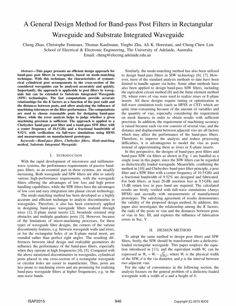
(a) (b)Fig. 4. Fabricated band-pass filters: (a) The post band-pass waveguide filter,(b) The SIW band-pass filter.
dimensions can be further optimized through space mappingtechnique or comparing the extracted coupling matrix with thetheoretical one [14] in order to have closer frequency responsesto ideal ones. However, since the calculated values already givesatisfactory results, no optimization is applied in this paper.The obtained values for the geometry variables of Fig. 1(a)and (b) are listed in Table I and Table II respectively. It isnoted that, in order to test the second filter, a microstrip-to-SIW transition as shown in Fig. 1(b) is designed by the methodintroduced in [15].
TABLE I. SIZES OF A BAND-PASS POST FILTER (UNITS: mm)
G1, G6 G2, G5 G3, G4 D1, D5 D2, D4 D3
8.42 6.57 6.01 14.64 17.00 17.50a b d
22.86 10.16 3
TABLE II. SIZES OF A BAND-PASS SIW FILTER (UNITS: mm)
G1, G6 G2, G5 G3, G4 D1, D5 D2, D4 D3
4.39 3.20 2.79 8.33 9.60 9.87Wi Wt Lt Ws d p b
13.91 5.29 14.12 2.08 1.00 1.80 0.762
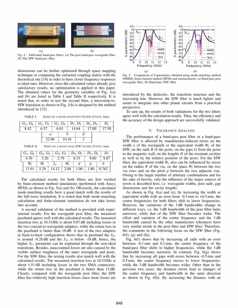
The calculated results for both filters are first verifiedby finite-element method simulations (performed with AnsysHFSS) as shown in Fig. 5(a) and (b). Obviously, the calculatedmode-matching results have a good match with the results ofthe full-wave simulation. It is noted that both mode-matchingcalculation and finite-element simulation do not take lossesinto account.
A second validation of the method is provided with exper-imental results. For the waveguide post filter, the measuredpassband agrees well with the calculated results. The measuredinsertion loss at 10.5 GHz is about 0.87 dB including losses inthe two coaxial-to-waveguide adapters, while the return loss inthe passband is better than 18 dB. A test of the two adaptersin back-to-back configuration shows that in passband the S21is around -0.28 dB and the S11 is below -18 dB, hence, thehigher S11 parameter can be explained through the non-idealtransitions. Besides, unaccounted losses are also caused by thevisible surface roughness of the inner waveguide and posts.For the SIW filter, the testing results also match well with thecalculated results. The measured insertion loss at 10.5 GHz isabout 1.51 dB including losses in the two SMA connectors,while the return loss in the passband is better than 15 dB.Clearly, compared with the waveguide post filter, the SIWfilter has relatively high insertion losses since more losses are
Frequency (GHz)
S p
ara
mete
rs (
dB
)
8 9 10 11 12 13-90
-80
-70
-60
-50
-40
-30
-20
-10
0
10
MMM
HFSS
Test
S11
S21
(a)
Frequency (GHz)
S p
ara
mete
rs (
dB
)
8 9 10 11 12 13-90
-80
-70
-60
-50
-40
-30
-20
-10
0
10
MMM
HFSS
Test
S11
S21
(b)Fig. 5. Comparison of S-parameters obtained using mode-matching method(MMM), finite-element method (HFSS) and measurements: (a) Band-pass postwaveguide filter, (b) Band-pass SIW filter.
introduced by the dielectric, the transition structure and themicrostrip line. However, the SIW filter is much lighter andeasier to integrate into other planar circuits from a practicalperspective.
To sum up, the results of both validations for the two filtersagree well with the calculation results. Thus, the efficiency andthe accuracy of the design approach are successfully validated.
V. TOLERANCE ANALYSIS
The performance of a band-pass post filter or a band-passSIW filter is affected by manufacture-induced errors on thewidth a of the waveguide or the equivalent width We of theSIW, on the radii R of the posts, on the gaps G from the poststo the magnetic wall, on the lengths D of the resonant cavitiesas well as by the relative position of the posts. For the SIWfilter, the equivalent width We also can be influenced by errorson the radius R of the via, on the space Wi between the twovia rows and on the pitch p between the two adjacent vias.Owing to the larger number of arbitrary combinations and forthe sake of brevity, only the influence of the major sources oferrors is described here, i.e. waveguide widths, post radii, gapdimensions and the cavity lengths.
As shown in Fig. 6(a) and (e), by increasing the width orequivalent width with an error from -0.5 mm to +0.5 mm, thecenter frequencies for both filters shift to lower frequencies.However, the variations of the 3 dB bandwidths change indifferent ways, i.e. the 3 dB bandwidth of the post filter turnsnarrower, while that of the SIW filter becomes wider. Theoffset and variation of the center frequency and the 3 dBbandwidth caused by the other manufacture tolerances havevery similar trends in the post filter and SIW filter. Therefore,the comments in the following focus on the SIW filter (Fig.6(f), (g) and (h)).
Fig. 6(f) shows that by increasing all radii with an errorbetween -0.1 mm and 0.1 mm, the center frequency of theband-pass filter shifts to higher frequencies, while the 3 dBbandwidth becomes narrower. In contrast, Fig. 6(g) showsthat by increasing all gaps with errors between -0.5 mm and0.5 mm, the center frequency moves to lower frequencies,while the 3 dB bandwidth becomes wider. Other than in theprevious two cases, the distance errors lead to changes ofthe centre frequency and bandwidth in the same directionas shown in Fig. 6(h). By increasing the distance with an
948

width error (mm)
Offset of centre frequency and
increment of 3dB bandwidth
-0.4 -0.2 0 0.2 0.4-0.08
-0.06
-0.04
-0.02
0
0.02
0.04
0.06
0.08center frequency3dB bandwidth
(GHz)
(a)
radius error (mm)
Offset of centre frequency and
increment of 3dB bandwidth
-0.24 -0.12 0 0.12 0.24-0.4
-0.3
-0.2
-0.1
0
0.1
0.2
0.3
0.4center frequency3dB bandwidth
(GHz)
(b)
gap error (mm)
Offset of centre frequency and
increment of 3dB bandwidth
-0.4 -0.2 0 0.2 0.4-0.15
-0.1
-0.05
0
0.05
0.1
0.15center frequency3dB bandwidth
(GHz)
(c)
distance error (mm)
Offset of centre frequency and
increment of 3dB bandwidth
-0.4 -0.2 0 0.2 0.4-0.2
-0.15
-0.1
-0.05
0
0.05
0.1
0.15
0.2center frequency3dB bandwidth
(GHz)
(d)
equivalent width error (mm)
Offset of centre frequency and
increment of 3dB bandwidth
-0.4 -0.2 0 0.2 0.4-0.15
-0.1
-0.05
0
0.05
0.1
0.15center frequency3dB bandwidth
(GHz)
(e)
radius error (mm)
Offset of centre frequency and
increment of 3dB bandwidth
-0.08 -0.04 0 0.04 0.08-0.25-0.2
-0.15-0.1
-0.050
0.050.1
0.150.2
0.25center frequency3dB bandwidth
(GHz)
(f)
gap error (mm)
Offset of centre frequency and
increment of 3dB bandwidth
-0.4 -0.2 0 0.2 0.4-0.2
-0.15
-0.1
-0.05
0
0.05
0.1
0.15
0.2center frequency3dB bandwidth
(GHz)
(g)
distance error (mm)
Offset of centre frequency and
increment of 3dB bandwidth
-0.4 -0.2 0 0.2 0.4-0.3
-0.2
-0.1
0
0.1
0.2
0.3
0.4center frequency3dB bandwidth
(GHz)
(h)Fig. 6. The offset of center frequency and variation of 3dB bandwidth caused by machining errors: (a) Width errors in the post filter, (b) Radius errors in thepost filter, (c) Gap errors in the post filter, (d) Distance errors in the post filter, (e) Equivalent width errors in the SIW filter, (f) Radius errors in the SIW filter,(g) Gap errors in the SIW filter, (h) Distance errors in the SIW filter.
error from -0.5 mm to +0.5 mm, both the center frequencyand the 3 dB bandwidth decrease. In addition, for the SIWfilter, the offset and variation also can be caused by the errorof the relative permittivity, e.g. specified by the manufactureras ±0.04. However, tests of this material parameter toleranceindicate that the impact of this error can be neglected.
VI. CONCLUSION
In this paper, the analysis and design of band-pass waveg-uide post filters and band-pass SIW filters have been consid-ered. Based on the mode-matching technique, the principle ofa common efficient design method has been presented for bothtypes of post filters. Applying this method, the K factors ofpost or via pairs placed in one cross-section of a rectangularwaveguide or SIW have been analyzed, including the influenceof manufacture tolerances. Based on the calculated relationshipbetween the K-factors and the structure dimensions, it isconvenient to choose reasonable posts or vias for designingband-pass filters, while the tolerance analysis allows to assessthe suitability of a machining process with a given precisionto fullfil a desired set of specifications. A Chebyshev band-pass post filter and a Chebyshev band-pass SIW filter havebeen designed and fabricated. The calculation results for bothfilters match well with the simulation results obtained withHFSS. The experimental data obtained with manufacturedprototypes for the two filters also show a good agreement withthe calculation results. The presented results demonstrate theviability and validity of the proposed design framework.
REFERENCES
[1] S. S. Park et al., “Design of 40 GHz-Band Iris-Type WaveguideBandpass Filter,” International Journal of Infrared and MillimeterWaves, vol. 24, no. 6, pp. 941–951, 2003.
[2] W. T. Zhang et al., “Design of Waveguide E-plane Hybrid MetalInsert Filters for Millimeter-Wave Application,” in 2010 InternationalConference on WCSP, Oct 2010, pp. 1–4.
[3] F. Arndt, J. Bornemann, D. Heckmann, C. Piontek, H. Semmerow, andH. Schueler, “Modal S-Matrix Method for the Optimum Design of In-ductively Direct-Coupled Cavity Filters,” IEE Proceedings Microwaves,Antennas and Propagation, vol. 133, no. 5, pp. 341–350, October 1986.
[4] J. Bornemann, U. Rosenberg, S. Amari, and R. Vahldieck, “ToleranceAnalysis of Bypass-, Cross- and Direct-Coupled Rectangular Waveg-uide Band-Pass Filters,” IEE Proceedings Microwaves, Antennas andPropagation, vol. 152, no. 3, pp. 167–170, June 2005.
[5] C. Zhao, T. Kaufmann, Y. B. Zhu, and C. C. Lim, “Efficient Approachesto Eliminate Influence Caused by Micro-Machining in Fabricating H-Plane Iris Band-Pass Filters,” in 2014 Asia-Pacific Microwave Confer-ence (APMC), Nov 2014, pp. 1306–1308.
[6] J. Bornemann and F. Taringou, “Substrate-Integrated Waveguide FilterDesign Using Mode-Matching Techniques,” in 2011 41st EuropeanMicrowave Conference (EuMC), Oct 2011, pp. 1–4.
[7] Z. Kordiboroujeni et al., “Efficient Mode-Matching Design ofSubstrate-Integrated Waveguide Filters,” in 2012 42nd European Mi-crowave Conference (EuMC), Oct 2012, pp. 253–256.
[8] X. Zou et al., “Design of An X-Band Symmetrical Window BandpassFilter Based on Substrate Integrated Waveguide,” in 2011 CSQRWC,vol. 1, July 2011, pp. 571–574.
[9] P. J. Qiu, Y. Zhang, and B. Yan, “A Novel Millimeter-Wave SubstrateIntegrated Waveguide (SIW) Filter Buried in LTCC,” in 2008 Asia-Pacific Microwave Conference (APMC), Dec 2008, pp. 1–4.
[10] C. Zhao, T. Kaufmann, Y. B. Zhu, and C. C. Lim, “ApproximationMethods for Cylindrical Posts in Rectangular Waveguides with ModeMatching Technique,” in 2014 IEEE Asia-Pacific Conference on AppliedElectromagnetics (APACE), Dec 2014, pp. 179–182.
[11] Y. Cassivi et al., “Dispersion Characteristics of Substrate IntegratedRectangular Waveguide,” IEEE Microwave and Wireless ComponentsLetters, vol. 12, no. 9, pp. 333–335, Sept 2002.
[12] J. Bornemann, F. Taringou, and Z. Kordiboroujeni, “A Mode-MatchingApproach for the Analysis and Design of Substrate-Integrated Waveg-uide Components,” Frequenz, vol. 65, no. 9-10, pp. 287–292, 2011.
[13] D. M. Pozar, Microwave Engineering, 4th ed. John Wiley & Sons,2011.
[14] R. J. Cameron et al., “Microwave Filters for Communication Systems:Fundamentals, Design, and Applications,” 2007.
[15] D. Deslandes, “Design Equations for Tapered Microstrip-to-SubstrateIntegrated Waveguide Transitions,” in 2010 IEEE MTT-S InternationalMicrowave Symposium Digest (MTT), May 2010, pp. 704–707.
949