a high-speed timing-aware router for fpgas
TRANSCRIPT

A High-Speed Timing-Aware Routerfor FPGAs
by
Jordan S. Swartz
A thesis submitted in conformity with the requirements
for the degree of Master of Applied Science
Department of Electrical and Computer Engineering
University of Toronto
© Copyright by Jordan S. Swartz 1998

Abstract
A High-Speed Timing-Aware Router for FPGAs
Master of Applied Science, 1998Jordan S. Swartz
Department of Electrical and Computer EngineeringUniversity of Toronto
Digital circuits can be realized almost instantly using Field-Programmable Gate Arrays
(FPGAs), but unfortunately the CAD tools used to generate FPGA programming bit-streams often
require several hours to compile large circuits. We contend that there exists a subset of designers
who are willing to pay for much faster compile times by having to use more resources on a given
FPGA, a larger FPGA, or some decrease in the circuit speed.
A significant portion of the compile time tends to be spent in the placement and routing
phases of the compile. This thesis focuses on the routing phase and proposes a new high-speed
timing-aware routing algorithm. The execution speed of the new router is very fast when the
FPGA contains at least 10% more routing resources than the minimum required by a circuit. For
example, when targeting a model of the Xilinx 4000XL FPGA, the routing time for a 250,000
gate circuit is 127 seconds on a 300 MHz UltraSPARC. The circuit delay is only 19% higher
compared to a high-quality timing-driven router.
Since some routing problems are inherently difficult and will unavoidably take a long time
to route, the practical use of high-speed routing requires that the tool must be able to predict if the
routing task is: (i) difficult and will take a long time to complete, or (ii) impossible to complete. In
this research, we present a method for making these predictions and show that it is accurate.
iii

iv

Acknowledgments
I would like to thank my advisor Jonathan Rose for providing direction, advice, and
encouragement. He has taught me a great deal about research, writing, and presenting. It was a
great privilege to work with him.
I owe a special thanks to Vaughn Betz who helped me in countless ways during my degree,
including: providing the VPR source code and supporting it, providing invaluable feedback and
insight into my work, editing this thesis, and for being so generous with his time.
I would also like to thank all of my friends and colleagues in the Computer and Electronics
Group, including: Alex, Ali, Andy, Dan, Dave, Guy, Jason A., Jason P., Javad, Jeff, Ken, Khalid,
Marcus, Mark, Mazen, Mike, Nirmal, Paul, Qiang, Rob, Sandy, Steve, Vincent, Warren, and
Yaska.
I am extremely grateful to my parents and my sisters for providing constant encouragement
and support during the past two years.
I would also like to acknowledge funding for this work from the Natural Sciences and
Engineering Research Council, Lucent Technologies Inc., MICRONET, and the University of
Toronto. I would also like to thank Dr. C.T. Chen for arranging my visit to Lucent.
v

vi

Table of ContentsChapter 1 Introduction........................................................................................................1
1.1 Thesis Organization ...................................................................................................3
Chapter 2 Background and Previous Work ......................................................................5
2.1 FPGA Architecture Terminology ..............................................................................5
2.2 Definition of the FPGA Routing Problem .................................................................7
2.3 Routing Algorithms ...................................................................................................8
2.3.1 Maze Routing Algorithm ..................................................................................8
2.3.2 Rip-Up and Re-Route Algorithm and Multi-Iteration Algorithm.....................9
2.3.3 Separated Global and Detailed Routers ............................................................10
2.3.3.1 CGE......................................................................................................10
2.3.3.2 SEGA ...................................................................................................11
2.3.3.3 FPR.......................................................................................................12
2.3.4 Combined Global and Detailed Routers ...........................................................14
2.3.4.1 TRACER ..............................................................................................14
2.3.4.2 GBP ......................................................................................................15
2.3.4.3 SROUTE ..............................................................................................16
2.3.4.4 Pathfinder .............................................................................................17
2.3.4.5 VPR ......................................................................................................19
2.3.5 High-Speed Compile Routers ...........................................................................23
2.3.5.1 Plane Parallel A* Maze Router ............................................................23
2.3.5.2 Negotiated A* Router...........................................................................24
2.4 Wirelength and Routability Prediction ......................................................................24
2.4.1 RISA ................................................................................................................24
2.4.2 Classification of Routing Difficulty.................................................................26
2.5 Xilinx XC4000XL Series of FPGAs..........................................................................27
2.5.1 Logic Block Architecture..................................................................................28
2.5.2 Routing Architecture.........................................................................................29
2.6 Summary ....................................................................................................................32
vii

Chapter 3 Routing Algorithm.............................................................................................33
3.1 Experimental FPGA Architectures ............................................................................33
3.1.1 Simple FPGA Architecture ...............................................................................34
3.1.2 4000X-like FPGA Architecture ........................................................................34
3.1.2.1 Logic-Block Architecture.....................................................................35
3.1.2.2 Routing Architecture ............................................................................36
3.1.2.3 Delay Model .........................................................................................37
3.2 Base Algorithm ..........................................................................................................38
3.3 Compile-Time Enhancements....................................................................................38
3.3.1 Directed Search.................................................................................................38
3.3.2 Fast Routing Schedule ......................................................................................43
3.3.3 Net Ordering .....................................................................................................44
3.3.4 Sink Ordering....................................................................................................44
3.3.5 Binning..............................................................................................................45
3.3.5.1 Bin Size ................................................................................................48
3.3.5.2 Empty Bins...........................................................................................49
3.3.5.3 Routing Architecture and Circuit Size Dependence ............................49
3.4 Circuit Delay Enhancements......................................................................................51
3.4.1 Switch Counting ...............................................................................................51
3.4.2 Track Segment Utilization ................................................................................54
3.5 Summary of Enhancement Effectiveness ..................................................................57
3.5.1 Simple Architecture ..........................................................................................57
3.5.2 4000X-Like Architecture ..................................................................................57
3.6 Summary ....................................................................................................................60
Chapter 4 Experimental Results.........................................................................................61
4.1 Benchmark Circuits ...................................................................................................61
4.2 Simple Architecture Experiments ..............................................................................62
4.2.1 Quality: Minimum Track Count .......................................................................62
4.2.2 Compile Time ...................................................................................................63
4.3 4000X-Like Architecture Experiments......................................................................66
4.3.1 Quality: Minimum Track Count .......................................................................66
4.3.2 Compile Time ...................................................................................................67
viii

4.3.3 Quality: Circuit Delay.......................................................................................68
4.3.4 Reducing the Compile Time .............................................................................70
4.4 Summary ....................................................................................................................71
Chapter 5 Practical Issues...................................................................................................73
5.1 Difficulty Prediction ..................................................................................................73
5.1.1 Estimating Total Wirelength.............................................................................74
5.1.2 Estimating Track Count ....................................................................................75
5.1.3 Difficulty Classification....................................................................................77
5.1.4 Demonstrations of Difficulty Prediction...........................................................78
5.2 Controlling the Difficulty of Routing Problems ........................................................82
5.3 Summary ....................................................................................................................86
Chapter 6 Conclusions.........................................................................................................89
6.1 Suggestions for Future Research ...............................................................................90
ix

x

List of FiguresFigure 2.1: (a) Island-style FPGA architecture, (b) connection box.....................................6
Figure 2.2: Switch boxes: (a) planar, (b) non-planar Wilton [5] ..........................................6
Figure 2.3: Example of segmented routing architecture.......................................................7
Figure 2.4: FPGA routing architecture and graph representation.........................................8
Figure 2.5: (a) Breadth-first search maze router, (b) directed search maze router ...............9
Figure 2.6: Three possible thumbnails for a 3x3 partitioning [20] .......................................13
Figure 2.7: Pseudocode for the Pathfinder routing algorithm [30].......................................19
Figure 2.7: Examples of correction factors...........................................................................25
Figure 2.8: Detailed view of a XC4000E/XL logic block [28].............................................28
Figure 2.9: Overview of routing for a logic block (shaded = 4000XL only) [28]................29
Figure 2.10: Detailed view of routing for a logic block [28]................................................31
Figure 3.1: (a) Simple FPGA routing architecture, (b) Simple FPGA logic block ..............34
Figure 3.2: 4000X-like logic block.......................................................................................35
Figure 3.3: Pseudocode for Directed Search Router.............................................................39
Figure 3.4: Example of ExpectedCost ..................................................................................41
Figure 3.5: Compile time vs. α for simple architecture........................................................42
Figure 3.6: Compile time and circuit delay vs. α, (a) low-stress routing problems,
(b) difficult routing problems, using the 4000X-like architecture......................43
Figure 3.7: Two methods of routing a multi-terminal net: (a) closest sinks first,
(b) furthest sinks first..........................................................................................45
Figure 3.8: Example of the binning technique......................................................................46
Figure 3.9: Average low-stress compile time vs. minimum binning fanout.........................47
Figure 3.10: Low-stress compile time vs. minimum binning fanout for circuits
spla and clma....................................................................................................50
Figure 3.11: Examples of routing use pass transistor and buffered switches .......................52
Figure 3.12: An example of counting pass transistor switches.............................................53
Figure 3.13: Example of SwichCount...................................................................................53
Figure 3.14: Average compile time vs. β, (a) low-stress routing problems,
(b) difficult routing problems, for 4000X-like architecture .............................55
xi

Figure 3.15: Example of the affect of different base costs ...................................................56
Figure 4.1: Compile time vs. available tracks for clma (8383 logic blocks) ........................65
Figure 4.2: (a) Compile time vs. % extra tracks, (b) Compile time vs.
% extra tracks (zoomed) .....................................................................................71
Figure 4.3: Circuit delay vs. % extra tracks...........................................................................72
Figure 5.1: Placement from VPR with 30% extra logic blocks............................................83
Figure 5.2: Placement with 30% extra logic blocks placed in columns ...............................84
Figure 5.3: Placement with 30% extra logic blocks placed in diagonals..............................85
xii

List of TablesTable 1.1: Place and route times for Xilinx M1 (using 300 MHz UltraSPARC) ..................2
Table 2.1: Correction factors for nets with up to fifty terminals [39]....................................25
Table 2.3: The XC4000E/XL family [28]..............................................................................27
Table 2.2: Routability predictors ...........................................................................................27
Table 2.4: Routing resources per logic block in 4000XL parts [28] .....................................30
Table 3.1: Track segments in 4000X-like architecture..........................................................36
Table 3.2: Compile times for different bin size scaling factors.............................................48
Table 3.3: Base cost of different routing resources ...............................................................56
Table 3.4: Effectiveness of directed search and binning for simple architecture ..................58
Table 3.5: Effectiveness of enhancements for 4000X-like architecture
(X enabled, -- disabled).........................................................................................59
Table 4.1: Benchmark circuits ...............................................................................................62
Table 4.2: Minimum track counts for the simple architecture...............................................63
Table 4.3: Compile times for simple architecture..................................................................64
Table 4.4: Minimum track counts for 4000X-like architecture .............................................67
Table 4.5: Compile times for 4000X-like architecture .........................................................68
Table 4.6: Circuit delays for 4000X-like architecture ..........................................................69
Table 5.1: Correction factors up to 50 for 4000X-like architecture ......................................75
Table 5.2: Utilization for simple architecture ........................................................................76
Table 5.3: Utilization for 4000X-like architecture ................................................................77
Table 5.4: Definition of routing classes.................................................................................78
Table 5.5: Track count estimates for the simple architecture ................................................79
Table 5.6: Track count estimates for 4000X-like architecture ..............................................79
Table 5.7: Difficulty prediction for simple architecture (LS=low-stress,
DF=difficult, IM=impossible)...............................................................................80
Table 5.8: Difficulty prediction for 4000X-like architecture (LS=low-stress,
DF=difficult, IM=impossible)...............................................................................81
Table 5.9: Results from 30% extra logic blocks experiments ...............................................86
Table 5.10: Results for increasing % extra logic blocks in diagonal pattern........................87
xiii

xiv

Introduction
Chapter 1
Introduction
Advances in technology over the past several decades have been driven by the fast pace of
growth in the microelectronics industry. One rapidly growing area of microelectronics is Field-
Programmable Gate Arrays (FPGAs), that allow digital circuits to be realized almost instantly.
FPGAs require the use of Computer-Aided Design (CAD) tools that transform a designer’s
high-level circuit description into a bit-stream used to program the FPGA. Unfortunately, as the
capacity of FPGAs has continued to increase, the CAD tools have become increasingly slower,
sometimes requiring the better part of a day to complete.
CAD tools for FPGAs usually consist of the following steps: logic synthesis, placement,
and routing [1]. The vast majority of the compile time tends to be spent in the placement and
routing steps. For example, Table 1.1 shows the total place and route times for a number of
MCNC benchmark circuits [2] using the Xilinx M1 CAD tool (version 4.12) [3]. All of the
compile times were measured on a 300MHz UltraSPARC processor. For each circuit the target
FPGA was filled to no more than 80% capacity, which should be considered a relatively easy
placement and routing task. The smallest circuit required approximately 4 minutes for placement
and routing. The largest circuit, which is approximately 5 times larger than the smallest circuit,
required more than one hour for placement and routing. This is 20 times longer than the compile
time for the smallest circuit.
For some designers, these compile times are too long. If the problem is any harder (higher
utilization of the FPGA), the compile times are known to exceed many hours. There is also some
evidence to suggest that compile time is a non-linear function of circuit size, such as the data in
Table 1.1, so the larger FPGAs of the future will take even longer to compile, despite anticipated
1

Introduction
increases in computer power. This work focuses on the routing portion of the compile and seeks to
develop a high-speed routing tool for FPGAs.
We can divide the set of FPGA designers into two classes: those who are willing to sacrifice
some result quality to obtain a large speedup in compile time; and those users who are not willing
to sacrifice any quality, regardless of the compile time. By sacrificing quality, we mean accepting
lower FPGA utilization and slower circuit speeds. We contend that there are a significant number
of users who are willing to sacrifice quality, and this work addresses those users. Note that even
users who demand high quality results could still use a high-speed routing tool to estimate
whether or not their circuit will fit in the target FPGA and to estimate the circuit speed, before
running a slower high-quality router.
The routing problem can be solved faster by reducing the demand on the FPGA routing
resources, which can be achieved by lowering the utilization of the FPGA. The utilization of an
FPGA can be lowered by either reducing the size of the circuit being targeted for the FPGA, or by
using a larger FPGA than needed to simply fit the circuit.
Another way in which the routing problem can be solved faster is by spending less effort
trying to optimize the critical path of a circuit. Routers that spend a significant amount of effort to
optimize the critical path of a circuit are known as “timing-driven” routers. We call routers that
obtain reasonable circuit speeds, without spending as much effort as a timing-driven router,
“timing-aware” routers.
An example of an application where users would be willing to trade FPGA utilization for a
large speedup in compile time is the FPGA-based custom computing world. In these applications,
highly-parallel computations are implemented in FPGAs to achieve a large run-time speedup
compared to running the computations using software. High-speed compile is crucial for FPGA-
based custom computing, because a standard software compiler runs in seconds or minutes. These
Table 1.1: Place and route times for Xilinx M1 (using 300 MHz UltraSPARC)
CircuitApproximateGate Count
Xilinx M1 (ver. 4.12)Place and Route
Time (s)
alu4 18,000 214
frisc 42,000 1038
s38417 76,000 1660
clma 100,000 4229
2

Introduction
users can lower the utilization of the FPGAs, in exchange for faster compile times, by using less
parallelism and hence less hardware. Less parallelism will increase the computation run-time, but
this will be offset by a large reduction in the FPGA compile time.
Another example of an application where high-speed compile is desperately needed is large
FPGA emulation systems, such as the Quickturn Mercury Design Verification System [4].
Emulation systems consist of hundreds of FPGAs that have to be compiled. Circuit speed is not
important, because the operating speed is limited by the large inter-FPGA routing delay. If the
user can tolerate having to use more FPGAs to realize their system, a significant compile-time
speedup is possible.
To assess how much result quality actual users of FPGAs would be willing to sacrifice for
high-speed compile, we posted a question to the usenet newsgroup “comp.arch.fpga”. We asked
designers whether they would be willing to trade some result quality to receive a routing
significantly faster (a few minutes as opposed to a few hours). Out of the seven responses, six of
the designers definitely wanted high-speed CAD tools, but all of designers were reluctant to trade
too much quality for faster results. Four of the respondents said that they would certainly use such
tools to get an idea of where their design stood during the design cycle, but would still use high-
quality CAD tools for the final compile.
The specific goal of this thesis is to develop a high-speed timing-aware router for FPGAs,
capable of routing a 250,000-gate circuit in under one minute. For the compile time to remain
extremely fast for even larger FPGAs, we also want to develop a routing algorithm with as near
linear run-time complexity as possible.
1.1 Thesis Organization
This thesis is organized as follows: Chapter 2 provides background information on previous
routing algorithms, routability prediction, and the commercial FPGA upon which one of our
experimental architectures is modeled. The routing algorithms, which are the basis for the new
high-speed routing algorithm, are described in detail.
Chapter 3 describes the new high-speed timing-aware routing algorithm.
Chapter 4 demonstrates the compile speed of the new high-speed router and makes
comparisons to two existing high-quality routers. It also compares the routability and circuit
speed of the new high-speed router to the same high-quality routers.
3

Introduction
Chapter 5 explores practical issues relating to the use of ultra-fast routing tools by actual
users. It describes a method of predicting how long a circuit will take to route and demonstrates
the accuracy and efficiency of the technique. This chapter also explores how the difficulty of a
routing problem changes as the logic capacity of the target FPGA increases.
Chapter 6 contains conclusions and suggestions for future work.
Figure 1.1:
(1.1)
4

Background and Previous Work
Chapter 2
Background and Previous Work
In this chapter, we begin by reviewing FPGA architecture terminology and giving a brief
definition of the FPGA routing problem. We then give an overview of many of the different
routing algorithms developed for FPGAs. We also review some work on routability prediction and
conclude with a description of the Xilinx XC4000XL FPGA architecture.
2.1 FPGA Architecture Terminology
All of the routing algorithms described in this chapter assume an FPGA architecture similar
to the island-style FPGA shown in Figure 2.1. The following terminology from Brown et al [1]
has become the standard method for describing an island-style FPGA architecture. Each logic
block has input and output (I/O) pins that connect to track segments through a connection box.
The number of track segments that a particular I/O pin connects to in a connection box is called
the connection box flexibility (Fc). The number of tracks per channel is W, which is also called the
track count. Figure 2.1 (a) shows the programmable connections for one connection box, with
Fc = 0.5W.
Track segments connect to other track segments through switch boxes. The number of track
segments that an incoming track segment connects to is called the switch box flexibility (Fs).
Figure 2.2 shows the connections for one track segment for two switch boxes with Fs = 3. A
switch box is called planar if it is impossible to leave a switch box on a different track number
then the one used to enter the switch box. Figure 2.2 (a) shows the connections for one track in a
planar switch box. In a planar architecture, the track number is selected in the connection box at
5

Background and Previous Work
the output pin of a logic block. A switch box is called non-planar if it is possible to leave a switch
box on a different track number then the one used to enter the switch box. Figure 2.2 (b) shows the
connections for one track in a non-planar switch box (track 0 is the incoming track), known as the
Wilton switch box [5]. In a non-planar architecture, it is possible to switch from one track number
to another track number in every switch box; these types of routing architectures improve
routability, as shown in [5].
FPGA architectures that contain multiple lengths of track segments are called segmented
routing architectures. For track segments that span more than one logic block, the track segment
will pass through one or more switch boxes without passing through a series switch. Figure 2.3
Logic Block
Connection Box
Switch Box
Figure 2.1: (a) Island-style FPGA architecture, (b) connection box
(a)
(b)
Channel SegmentTrack Segment
012
012
0 1 2
0 1 2
012
012
0 1 2
0 1 2
Figure 2.2: Switch boxes: (a) planar, (b) non-planar Wilton [5]
(a) (b)
6

Background and Previous Work
shows an example of part of an FPGA with a segmented routing architecture containing a single-
length, double-length, and quad-length track segment.
2.2 Definition of the FPGA Routing Problem
Many of the routing algorithms described in this chapter were designed by considering the
routing problem as finding a path for each net through a directed graph (G). Figure 2.4 shows a
small portion of an FPGA and its representation as a graph. The logic blocks (A, B), the I/O pins
(OP, IP1, IP2), and the track segments (1, 2, 3, 4, 5) are represented as a set of nodes (V) and there
is a set of directed edges (E) representing possible connections between the various routing
resources.
The routing problem is defined as follows: for a circuit to be successfully routed in an
FPGA, a path through the routing graph G must be found for every net to connect from its source
terminal to every one of its sink terminals. The paths for different nets are usually chosen to
minimize the total number of track segments required by the circuit and possibly to minimize the
circuit delay. A path for a net is legal if every node in the path is used by at most one net (except
for logic block nodes which may be the start or end of multiple nets). For a circuit to be
successfully routed, legal routes must be found for every net.
The routing problem is difficult to solve, since the choice of a certain path for one net may
block the best paths for other nets or possibly make it impossible to route other nets without over-
using certain routing resources. Routing congestion occurs when a routing resource, such as a
track segment or an I/O pin, is over-used.
Figure 2.3: Example of segmented routing architecture
Single
Double
Quad
Series SwitchLogic Block
Switch Box
7

Background and Previous Work
2.3 Routing Algorithms
In this section, we describe many of the academic routing algorithms developed for FPGAs.
We start with a description of the basic maze routing algorithm, the rip-up and re-route algorithm,
and the multi-iteration algorithm, which are the basis for many of algorithms described in this
section. We then review a number of algorithms, sub-divided into two classes: separated global
and detailed routers, and combined global and detailed routers. Finally, two algorithms designed
specifically to reduce execution time are described.
2.3.1 Maze Routing Algorithm
The maze router, developed by Lee [6], is the basis for many of the routing algorithms
described in this section. The maze routing algorithm was designed to find the shortest path
between two points on a rectangular grid, using a breadth-first search. The algorithm is
guaranteed to find a path, if one exists. When applied to an FPGA, the maze routing algorithm
starts at the source node of a net and expands each neighboring node. The neighboring nodes of
each expanded node are then expanded. Expansions continue until the sink node of the net is
reached, or all nodes have been visited and no path has been found.
A B
1
2 3
A
B
OP
2
3
Figure 2.4: FPGA routing architecture and graph representation
Logic Block
Switch
Track Segment4 5
1
IP1
4
5
IP2
OP IP1IP2
8

Background and Previous Work
One of the biggest weaknesses of this algorithm is that it can be very slow, since a large
number of the nodes in a graph will have to be visited to route a net. There have been various
improvements to the basic maze router to improve the run-time. Rubin showed that using a depth-
first search could significantly reduce the run-time, while still finding the shortest path between
two nodes [8]. Rubin also showed that when routing a two-terminal net, the selection of the
starting terminal for the search can significantly reduce the run-time. Choosing a terminal located
closer to one of the four corners of the rectangular grid helps to reduce the run-time since the
edges of the grid impose boundaries on the search.
Soukup [7] altered the basic algorithm to make it expand nodes that were successively
closer to the sink of a net, creating a directed search algorithm. Soukup showed that a directed
search algorithm provides an order of magnitude speedup over the basic maze routing algorithm.
Figure 2.5 shows an example of how the maze router expansions would proceed for (a) a breadth-
first search and (b) a directed search. The source of the net is marked with an “S” and the target
sink is marked with a “T”. The black squares mark blocked nodes or congestion. The directed
search expands significantly fewer nodes than the breadth-first search, since the search expands
directly towards the target sink. If there is a significant amount of congestion, the directed search
may end up expanding most of the nodes to find a path to the target sink. In the worst case, the
directed search has to expand as many nodes as the breadth-first search.
2.3.2 Rip-Up and Re-Route Algorithm and Multi-Iteration Algorithm
Since the routing resources in an FPGA are limited, routing algorithms face the problem of
dealing with routing congestion. The problem is that routing one net using particular resources
S
T
11
112
2 2
22
2
2
2 33
33
33
33
33
3
S
T
11
11
2
22 33
34
4
45
5
56
6
6
Figure 2.5: (a) Breadth-first search maze router, (b) directed search maze router
(a) (b)
9

Background and Previous Work
may make it impossible to route some other nets. There have been two main types of algorithms
to deal with the congestion problem. The first type of algorithm is known as rip-up and re-route,
such as the work done by Linsker [9] or Kuh and Marek-Sadowska [10]. With rip-up and re-route
algorithms, nets using resources that are congested are ripped-up and re-routed. The success is
dependent on the choice of which nets to rip-up and the order in which ripped-up nets are re-
routed.
Another solution to the congestion problem, known as the multi-iteration approach, was
conceived by Nair [11]. A routing iteration is the ripping-up and re-routing of every single net.
The nets are not ripped-up all at once, but instead each net is ripped-up separately (leaving all the
other nets in place) and re-routed. Several iterations are performed to alleviate routing congestion.
Nets are routed in the same order in each iteration, but only one net is ripped-up at a time.
Congestion is identified by keeping track of the number of nets currently occupying each routing
resource node. Any node with an occupancy greater than one is considered congested. Nair’s
technique is very effective for resolving congestion problems, because nets in non-congested
areas can also be relocated to allow nets using congested resources to be routed more easily.
Now that we have described some of the basic techniques used by many routing algorithms,
in the next two sections we describe several routing algorithms in more detail.
2.3.3 Separated Global and Detailed Routers
The following routing algorithms are classified as separated global and detailed routers.
Here the solution to the routing problem is performed in two steps to make the problem easier to
solve. A global routing algorithm is first applied to choose channel segments (see Figure 2.1a) for
routing each net, without choosing the exact tracks and switches within each channel. After global
routing, a detailed routing algorithm is used to choose the exact tracks and switches. The detailed
router is usually restricted to routing nets using the channel segments chosen by the global router.
2.3.3.1 CGE
The Course Graph Expansion (CGE) routing algorithm, developed by Brown et al [12], is
the first academic routing algorithm developed for island-style FPGAs. CGE is a routability-
driven router, although timing critical nets can be assigned a higher priority in the routing
algorithm.
10

Background and Previous Work
The global routing algorithm used by CGE is the LocusRoute global routing algorithm for
standard cells [13]. In the LocusRoute algorithm, multi-terminal nets are broken up into two-
terminal nets. Each two-terminal net is then routed using a minimum length path. Paths are
chosen so as to balance the nets among all the channels.
The CGE detailed routing algorithm is divided into two steps. In the first step, each global
route is expanded into a set of alternative detailed routes--each makes specific choices of track
segments and switches. For some nets, there may be a vast number of possible detailed routes, so
a pruning algorithm is used to limit the number of detailed routes stored for each net (this reduces
the memory requirements and speeds up the algorithm). In the second step, a detailed route is
chosen for each net; the detailed route with the fewest routing resources used by detailed routes
for other nets is chosen. The router also takes into account nets that have only one possible
detailed route and nets that are timing critical. After choosing a detailed route for a net, all of the
other nets are updated to remove any detailed routes that use any of the resources just allocated. If
it is impossible to route any nets, then multiple iterations with rip-up and re-route are attempted.
Only nets using the congested channel segments are ripped-up and re-routed. For the ripped-up
nets, new detailed routes are expanded using less aggressive pruning for each successive iteration.
The experimental architecture used for testing CGE was similar to the Xilinx 3000 series
FPGA [14]. All the track segments were single-length segments with Fs=6 and Fc=0.6W.
Comparisons were made to a maze routing algorithm, where the maze router was restricted to
using track segments within the same global routes as CGE. CGE was able to route a set of
benchmark circuits in an average of 35% less tracks per channel compared to the maze router.
2.3.3.2 SEGA
The Segment Allocator (SEGA) routing algorithm [15] [16] is an extension of the CGE
algorithm to target FPGAs with segmented routing architectures.
The global router used with SEGA is almost identical to that used with CGE. One important
enhancement is the addition of bend reduction to penalize any bends in the global route for a net
[17]. Since the underlying routing architecture contains some track segments which are longer
than unit length, a global route with fewer bends allows the detailed router to use longer track
segments. Bend reduction was shown to significantly reduce the total number of tracks per
channel required by circuits, compared to not using bend reduction.
11

Background and Previous Work
The detailed router for SEGA is based on the same principal as CGE, in that the global
routes are expanded into a set of detailed routes for each two-terminal net and one detailed route
is chosen for implementing each two-terminal net. However, besides a cost function to minimize
congestion, SEGA also contains two cost functions for minimizing circuit delay that make the
router timing-aware. The first cost function contains two terms: one term to prefer longer track
segments to cover a long distance, rather than several short segments; and the other term to make
sure that a long segment is not wasted to go a very short distance. The other cost function uses the
Rubinstein-Penfield delay model [18] for calculating the delay of a net. The delay is calculated for
each possible detailed route of a two-point connection, and the fastest route is chosen.
Another enhancement in SEGA versus CGE is a method to reduce the wirelength and delay
of multi-terminal nets. In CGE, all of the two-terminal nets that were decomposed from multi-
terminal nets may be routed in any order. Little effort is made to re-use track segments of two-
terminal nets that are actually part of the same multi-terminal net. Re-using track segments can
significantly reduce the track count as well as the circuit delay. To re-use track segments, all of the
two-terminal nets comprising a multi-terminal net are routed together, with the largest multi-
terminal nets routed first (where the size is the sum of the estimated length for each two-terminal
net.) The two-terminal nets are routed in order from longest to shortest. As the routing proceeds,
track segments used for other two-terminal nets that are part of the same multi-terminal net are re-
used as much as possible.
Experiments with SEGA were run on an FPGA architecture similar to the Xilinx 4000
series FPGA [14], containing single-length, double-length, and long-length track segments, with
Fs=3 and Fc=W. There were no other results to compare with at the time of this work, although
experiments showed how the various enhancements significantly improved the track count and
delay of circuits.
2.3.3.3 FPR
FPR, developed by Alexander et al [20], is a combined placement and global routing
algorithm, followed by detailed routing. This algorithm, which is purely routability-driven, tries
to simultaneously optimize source-sink pathlength, total wirelength, and track count.
The combined placement and global routing algorithm is based on a technique called
thumbnail partitioning. The basic idea is that the entire FPGA is divided into a 3 x 3 grid, where
12

Background and Previous Work
each logic block is contained in exactly one region of the grid. The placement of logic blocks is
improved using simulated annealing [19] to move logic blocks between regions. Each region is
then subdivided into 3 x 3 sub-regions and simulated annealing is used on the sub-regions. Each
region is recursively subdivided and improved, until each region contains exactly one logic block.
The cost function for the placement algorithm uses pre-computed 3 x 3 Rectilinear Steiner
Arborescences1 (RSA) [23], also called thumbnails, that connect all of the net terminals across
partition boundaries. One thumbnail is chosen for each net; the objective is to minimize the total
source-sink pathlength and the total wirelength across all of the nets, while also balancing
congestion between adjacent regions. If a net has more than one terminal in a region, they are
counted as one terminal. Figure 2.6 shows an example of three possible thumbnails for a set of
points in a 3 x 3 partitioning.
Once the placement algorithm has completed and each region contains exactly one logic
block, global routing can be performed using the thumbnails assigned to nets at each level of
recursion. At each level of recursion, a switch box is assigned to each point where a thumbnail
crosses a partition boundary. The maximum number of nets assigned to each switch box along a
boundary is calculated by taking the total number of nets crossing the boundary divided by the
number of switch boxes along the boundary. Once the lowest level of recursion is reached, every
net will have a global route assigned.
The detailed routing algorithm assigns specific track segments and switches to each net,
within the channel segments and switch boxes specified by the combined placement and global
routing algorithm. Each net is routed one at time, using a Steiner tree construction method known
as Iterated-KMB (IKMB) [21]. If a net is impossible to route within the channel segments chosen
by the global router, then the detailed router is allowed to use channel segments outside the
1. An RSA is a rectilinear tree that contains the shortest path from the source terminal to each sink terminal [23].
Figure 2.6: Three possible thumbnails for a 3x3 partitioning [20]
Thumbnail
PartitionBoundary
13

Background and Previous Work
chosen global route. If a net is still unroutable, then all of the nets are routed again, routing the
unroutable nets first. The detailed router tries a number of iterations before declaring failure.
IKMB is based on the Kou, Markowsky and Berman (KMB) algorithm [22]. The KMB
algorithm constructs Steiner trees which are within twice the cost of the optimal Steiner tree, in
polynomial time. For a net, IKMB (in the context of FPGAs) iteratively tries many of the switch
boxes in the net as possible Steiner points. The switch boxes that reduce the cost of the net by the
largest amount are chosen as the final Steiner points.
Using an architecture similar to the Xilinx 3000 series FPGA, FPR was only an average of
4% better than CGE at minimizing track count across a number of benchmark circuits. Using an
architecture similar to the Xilinx 4000 series FPGA, comparisons were made to SEGA and GBP
(see Section 2.3.4.2). FPR was 13% better, on average, than SEGA at minimizing track count.
FPR was only an average of 6% better than GBP at minimizing track count.
2.3.4 Combined Global and Detailed Routers
Routers that use separate global and detailed routing algorithms may suffer what is termed
the mapping anomaly [27]. Since the global router does not know the details of the switch box and
connection box architecture, the detailed router may not be able to route all of the nets using the
assigned global routes. Combined global and detailed routers do not suffer from the mapping
anomaly, since decisions about the channel segments and the specific track segments and switches
are made at the same time. In this section, we describe a number of combined global and detailed
routing algorithms.
2.3.4.1 TRACER
The TRACER routing algorithm, designed by Lee and Wu [24], is a timing-driven
algorithm. The routing algorithm is split into three steps: delay and congestion estimation; initial
routing; and rip-up and re-routing.
The purpose of the delay and congestion estimation step is to determine a criticality for each
net based on the estimated minimum delay for each net and the amount of congestion a net may
have to avoid for successful routing. Each net is routed using a breadth-first maze routing
algorithm, ignoring any over-use of routing resources. Since each net is allowed to use the best
routing resources, a measure of the minimum delay and the slack [25] of each net can be
14

Background and Previous Work
calculated. For the delay calculations, full path-based timing analysis is performed, using an
implementation of the Elmore delay model [26]. The congestion for each net is calculated based
on the use of the routing resources (by all of the nets) contained within the bounding box of the
net.
In the second step, each of the nets is routed again, using a breadth-first maze router. The
nets are routed in order of decreasing criticality. Routing resources are not allowed to be over-
used, unless there is no other way to route a net.
The final step, rip-up and re-routing, is divided into two parts: congestion resolution and
delay resolution. In congestion resolution, a rip-up and re-route approach is used to try and
resolve any congestion problems from the initial routing. A simulated-evolution algorithm is used
to choose which nets to rip-up and re-route. Nets are selected randomly to be ripped-up and re-
routed, so that any net may be selected for rip-up and re-route, not just the nets using congested
resources. Nets that have a much larger wirelength compared to the minimum estimated
wirelength or nets using a large number of over-used routing resources, have a higher likelihood
of being chosen for rip-up. The simulated evolution algorithm continues until there are no more
routing resources over-used or a time limit is exceeded and failure is declared.
In delay resolution, nets that are part of paths where the timing constraints have been
exceeded are ripped-up and re-routed, using a similar algorithm to congestion resolution. Nets on
paths that exceed the timing constraints and nets on paths that are well under the timing
constraints have a higher likelihood of being chosen for rip-up. Again, either the constraints are
met or failure is declared after exceeding a time limit.
The FPGA architecture used for testing TRACER was an island-style FPGA with all single-
length track segments and Fc=W and Fs=3. Experiments were run on a set of small benchmarks
circuits and comparisons made to CGE and SEGA. Compared to CGE and SEGA, TRACER
reduced the average track count by 29% and the average circuit delay by 27%.
2.3.4.2 GBP
The Greedy Bin Packing (GBP) routing algorithm, by Wu and Marek-Sadowska [27], is a
routability-driven router. In this work, the routing problem is considered as a bin packing
problem, where the bins are the routing tracks. The goal is to fill each of the bins with as many
nets as possible and to use as few bins (routing tracks) as possible.
15

Background and Previous Work
The algorithm starts by breaking multi-terminal nets into two terminal nets. A confronting
graph is created, where each net is a node and there are edges between nodes where two nets have
pins in the same channel segment. Nets are then packed into bins (tracks), based upon information
from the confronting graph and the length of nets. Nets are placed in only one bin at a time, until
that bin full.
One important assumption made in this work is that the routing architecture is planar (see
Section 2.1), otherwise it is not possible to use this routing algorithm. At the time that this work
was completed, the Xilinx 4000 architecture was a planar architecture, but newer architectures
such as the Xilinx 4000XL [28] are non-planar.
GBP reduced the average track count by 17%, on average, compared to CGE and SEGA.
GBP required 30% more tracks per channel, on average, compared to TRACER.
2.3.4.3 SROUTE
SROUTE, developed by Wilton [5], is a routability-driven router designed for exploring
FPGA architectures with embedded memory. SROUTE is able to target island-style architectures
and is also moderately fast.
In the SROUTE algorithm, multiple routing iterations are used to resolve congestion, during
which every net is re-routed. During the first iteration, the nets are routed in the given order.
During successive iterations, nets that could not be routed in the previous iteration are routed first.
The inner-loop of the router uses a directed search maze router. The cost function for the directed
search algorithm is based on the Manhattan distance to the target. Multi-terminal nets are routed
one sink at a time, starting with the sink closest to the source of the net. For subsequent sinks, the
sink that is closest to any part of the existing net is chosen as the next target; routing is continued
from the part of the net closest to this target. If the directed maze router should fail to route a net,
then a breadth-first maze router is used to try and route the net.
Experiments were run using a planar architecture with only unit length track segments,
Fs=3, and Fc=W. SROUTE was able to route as set of benchmark circuits using 16% less tracks
per channel, on average, compared to SEGA; 15% less tracks per channel, on average, compared
to GBP; and 9% less tracks per channel, on average, compared to FPR. SROUTE required 11%
more tracks per channel, on average, compared to TRACER. Experiments were also run that
16

Background and Previous Work
measured up to a 5 times speedup in execution time compared to a purely breadth-first search
maze router.
2.3.4.4 Pathfinder
The Pathfinder routing algorithm, designed by Ebeling et al [30], is both a routability-driven
and a timing-driven router. While the Pathfinder algorithm was designed to target the specialized
Triptych FPGA architecture [31], it is a general routing algorithm that can be applied to almost
any type of FPGA architecture. One of key differences between this work and previous work is
that the Pathfinder algorithm tries to simultaneously optimize track count and circuit delay. We
give more detail about this algorithm compared to the other algorithms, because much of our
work is built upon the Pathfinder algorithm.
The Pathfinder algorithm is based upon Nair’s method of iterative maze routing for custom
integrated circuits [11]. During each iteration, every net is ripped-up and re-routed, in the same
order during each iteration. During early iterations, nets are allowed to share routing resources
with other nets. As the iterations proceed, the sharing of routing resources is penalized, increasing
gradually with each iteration. (Note that Nair’s algorithm does not allow routing resources to be
overused.) After a large number of iterations (up to a few hundred), the nets will negotiate among
congested resources to try and find a way to successfully route the circuit, allocating key
resources to the nets that need them the most. By re-routing all of the nets during each iteration,
nets that do not absolutely require congested routing resources can also be relocated.
The basic Pathfinder algorithm routes nets using a breadth-first maze routing algorithm. A
cost function is applied to each node (routing resource) to try and minimize congestion and the
delay of more critical nets. The cost function, C(n), applied to each node n by the maze router is:
(2.1)
where d(n) is the intrinsic delay of node n, Cost(n) is the congestion cost of using node n, and
A(i,j) is the slack ratio from the source of net i to the jth sink of net i. The congestion cost is calcu-
lated as:
(2.2)
where b(n) is the base cost of using node n (set to the intrinsic delay of node n), h(n) is the histor-
ical congestion penalty based upon the over-use of node n during previous routing iterations, and
p(n) is the present congestion penalty based on the over-use of node n during the current routing
C n( ) A i j,( ) d n( )⋅ 1 A i j,( )–[ ] Cost n( )⋅+=
Cost n( ) b n( ) h n( )+[ ] p n( )⋅=
17

Background and Previous Work
iteration. The exact methods for calculating p(n) and h(n) were not given in [30].
The slack ratio is defined as:
(2.3)
where D(i,j) is the longest path delay through the circuit that contains the path from the source of
net i to the jth sink and Dmax is the critical path delay of the circuit. If a connection lies on the crit-
ical path, then A(i,j) will equal 1.0, and cost function Equation (2.1) will be weighted completely
towards optimizing delay. If a connection lies on a path with a large slack, and is therefore non-
critical, A(i,j) will approach 0, and the cost function (2.1) will be heavily weighted towards mini-
mizing congestion. A value of A(i,j) between 0 and 1 will cause the router to try and minimize
both delay and congestion. Note that setting A(i,j) to 0 for all nets makes the router completely
routability-driven.
Figure 2.7 shows pseudocode for the complete Pathfinder routing algorithm. For the first
iteration of the router, all of the nets are marked as critical by setting A(i,j) to 1 for all nets (line 1).
For each net there is an associated routing tree (RT) that stores the path to each sink in the net. On
line 5, the RT for net i is initialized with just the source of the net. The loop from lines 6 to 16
performs the routing to each sink of net i. The source-sink paths with the largest slack ratios (most
critical) are routed first. When routing to a sink, all of the routing resources already in the RT are
added to the priority queue (PQ), so that routing to the next sink may continue from any resource
already part of the net (line 7). The loop from lines 8 to 12 explores the routing graph until the
target sink is reached. Once the target sink is reached, the congestion cost for all the nodes on the
new path are updated and the nodes are added to the RT (lines 13 to 16). At the end of each
iteration, all of the path delay and slack ratios are recalculated (line 19), so that the router can
adjust the cost function of Equation (2.1) to try and balance congestion and circuit delay.
Two enhancements are described in [30] to increase the execution speed of the Pathfinder
algorithm. The first enhancement adds a directed-search term to the cost function used for routing
nets. The directed-search term used is a lower bound on the cost given by Equation (2.1). This
allows the router to choose nodes that are successively closer to the target sink, which reduces the
run-time compared to a breadth-first search. The second enhancement is to re-route only the nets
that are using congested nodes during successive iterations, instead of re-routing every net. This
requires more iterations to successfully route a circuit, but each iteration is faster, resulting in a
small reduction in the run-time.
A i j,( ) D i j,( ) Dmax⁄=
18

Background and Previous Work
In [32], experiments were run targeting the Xilinx 3000 series FPGA. In these experiments,
the track counts were fixed and comparisons were made between the implemented circuit speeds
of Pathfinder versus the Xilinx routing tool. Pathfinder was shown to provide about 11% better
circuit speed on average. No comparisons were made to any of the other routers described in this
chapter.
2.3.4.5 VPR
The Versatile Place and Route (VPR) tool, designed by Betz et al [34] [33], is a complete
place and route system designed for exploring FPGA architectures. The router is based primarily
on the Pathfinder routing algorithm, with some key enhancements to improve the track count,
circuit speed, and compile time. VPR contains two routers: one router is routability-driven, and
the other router is timing-driven. We describe VPR’s routing algorithms in detail for two reasons:
first, our work was incorporated into the VPR code base, re-using much of the routing algorithm
code and using the placement tool and the architecture generation algorithms; second, we use
VPR as our basis for experimental comparisons.
[1] A(i,j) ← 1 for all net sources i and sinks j[2] While shared resources exist[3] Loop over all net sources i[4] Rip up routing tree RT(i)
[5] RT(i) ← net source i[6] Loop over all sinks t(i,j) in decreasing A(i,j) order
[7] PQ ← RT(i) at cost A(i,j)·d(n) for each node n in RT(i)[8] Loop until t(i,j) is found[9] Remove lowest cost node m from PQ[10] Add all neighboring nodes n of node m to PQ with[11] cost = Cost(n) + path cost from source to m[12] End[13] Loop over nodes n in path t(i,j) to source i (backtrace)[14] Update Cost(n)[15] Add n to RT(i)[16] End[17] End[18] End[19] Calculate path delay and A(i,j)[20] End
Figure 2.7: Pseudocode for the Pathfinder routing algorithm [30].
19

Background and Previous Work
The routability-driven routing algorithm in VPR is very similar to the breadth-first
routability-driven Pathfinder algorithm, with a few important changes and enhancements.
The first enhancement is a change to the congestion cost function used for evaluating a
routing resource node n. The congestion cost function used by VPR is:
(2.4)
where b(n), h(n), and p(n) are the base cost, historical congestion penalty, and present congestion
penalty, as defined in Section 2.3.4.4. Equation (2.4) is different from Equation (2.2) in that all the
terms are multiplied together rather than adding b(n) and h(n), to avoid having to normalize b(n)
and h(n).
In Pathfinder, the base costs of routing resource nodes are set to their intrinsic delay values.
VPR sets the bases costs of almost all of the routing resources to 1. The only exceptions are input
pins, which are given a base cost of 0.95. This causes the router to expand any input pins reached
first and speeds up the routability-driven router by up to 1.5 to 2 times. The base costs used by
VPR resulted in a 10% average decrease in track count, compared to using the original Pathfinder
base costs.
The present congestion penalty, p(n), is calculated by VPR as:
(2.5)
where occupancy is the number of nets presently using node n, capacity(n) is the maximum num-
ber of nets that can legally use node n, and pfac is a value that scales the present congestion pen-
alty. The present congestion penalty is updated whenever a net is ripped-up and re-routed.
The historical congestion penalty, h(n), is calculated by VPR as:
(2.6)
where i is the iteration number, and hfac is a value that scales the historical congestion penalty.
The historical congestion penalty is updated after each routing iteration.
The values of pfac and hfac comprise what is called the routing schedule [33]. Normally, the
default routing schedule of VPR is used, where the value for pfac is set to 0.5 or less in the first
iteration and increased by 1.5 to 2 times in subsequent iterations [33]. The value of hfac is set to
any value between 0.2 and 1, and remains constant in subsequent iterations [33]. With the default
routing schedule, VPR usually requires several iterations to route a circuit. The router can be sped
Cost n( ) b n( ) h n( ) p n( )⋅ ⋅=
p n( ) 1 max 0 occupancy n( ) 1 capacity n( )–+[ ] p fac⋅,( )+=
h n( )i1 i, 1=
h n( )i 1–max 0 occupancy n( ) capacity n( )–[ ] h fac⋅,( ) i 1>,+
=
20

Background and Previous Work
up by two to three times by setting pfac and hfac to 10000, called the fast routing schedule. The fast
routing schedule forces the router to avoid over-using routing resources if possible, resulting in a
reduction in the number of routing iterations. For easy problems, the router can sometimes route
the circuit in just one iteration. The fast routing schedule typically requires only 2% to 4% more
tracks over the best track count for a circuit by VPR.
Another important enhancement in VPR versus Pathfinder is the manner in which the
routing tree is placed back on the priority queue when routing a multi-terminal net. Recall that the
Pathfinder algorithm empties the PQ after each sink is reached in a multi-terminal net, and puts
the complete RT back on the PQ (see Figure 2.7, line 7). For very high-fanout nets, the RT is very
large, requiring significant CPU time simply to place the RT on the PQ for each sink. VPR
contains a much more efficient method, called the optimized breadth-first search, where the PQ is
left in its current state after reaching a sink, and just the new portion of the routing used to reach
the new sink is added back onto the PQ. The search for the next sink is then continued as normal.
The optimized breadth-first search enhancement results in an order-of-magnitude speedup,
compared to using the regular breadth-first search.
In comparison to all of the other routers described in this chapter, VPR is able to achieve the
lowest track counts across a series of smaller benchmark circuits, containing circuits with up to
358 logic blocks. The routability-driven VPR router obtained a 10% lower track count, on
average, compared to the next best router, TRACER. Using the VPR global router with the
detailed router of SEGA, the routability-driven VPR router achieved a 14% lower track count, on
average, compared to SEGA. Using a series of much larger benchmark circuits containing up to
8383 logic blocks, VPR used 70% fewer tracks per channel, on average, compared to SEGA.
The timing-driven routing algorithm of VPR is also based upon Pathfinder, but the timing-
driven component is handled differently by VPR. In Pathfinder, a linear delay model is used,
where each routing resource has a constant delay and the delays are summed to find the path
delay. For track segments that are connected using buffers, the linear delay is accurate. But, for
track segments that are connected using pass transistors, the linear delay model is highly
inaccurate, because it fails to take into account the fact that the delay through a pass transistor
depends on the other elements connected to the pass transistor. It is shown in [33] how the linear
delay model causes the router to choose incorrect paths among alternatives. VPR uses the Elmore
delay model [26], which models the delay of pass transistors more accurately than the linear delay
model. The cost function used by the timing-driven routing algorithm in VPR is:
21

Background and Previous Work
(2.7)
where crit(i,j) is the criticality of the net being routed, d(n,Elmore) is the elmore delay of node n,
and Cost(n) is the congestion cost of node n as given in Equation (2.4). Unlike the intrinsic delay
value which is constant, the Elmore delay must be calculated dynamically, depending on the
structure of the routing resources used to reach this node n. The criticality serves the same pur-
pose as the slack ratio in Pathfinder, it is used to balance congestion and timing optimization. The
criticality is defined as:
(2.8)
where slack(i,j) is the slack between the source of net i and the sink j, and Dmax is the critical path
delay of the circuit. VPR sets the maximum criticality value to 0.99 so that no net will completely
ignore congestion.
Since the Elmore delay depends on the exact structure of connections for a net and the net is
being changed as each sink is routed, it is necessary to update the Elmore delay of each node in
the net after routing each sink in the net. Referring to Figure 2.7, the Elmore delays for all the
nodes in RT(i) would be updated after reaching each sink in a net (line 16).
The optimized breadth-first search describe for the routability-driven router cannot be
utilized with the timing-driven router, since the Elmore delay which must be updated for all the
nodes in the current expansion after reaching each sink in the net. Since placing the whole routing
tree back on the priority queue for each sink of a net and re-starting the breadth-first search is very
time consuming, a directed search is used instead of a breadth-first search. The decision to
implement a directed search was based on results from the present research in [36] that showed a
large speedup in the compile-time from using a directed search within the Pathfinder algorithm.
The directed search uses an estimate of the total cost given by Equation (2.7) to reach the target
sink. The estimate assumes that connections of the same length or type as the current node being
expanded will be used to reach the target sink and that the shortest path will be used. Using the
directed search, the timing-driven VPR router is 10 times faster, on average, compared to the
routability-driven VPR router.
Comparisons were made between the routability-driven and timing-driven routers of VPR,
using a model of the Xilinx 4000XL FPGA, developed as part of the present research. In
comparing the two routers, the timing-driven VPR router produced circuits with 2.5 times less
c n( ) crit i j,( ) d n Elmore,( )⋅ 1 crit i j,( )–[ ] Cost n( )⋅+=
crit i j,( ) min 1 slack i j,( )Dmax
--------------------------– 0.99,
=
22

Background and Previous Work
delay, on average, than the routability-driven VPR router. The timing-driven VPR router only
required 6% extra tracks per channel, on average, compared to the routability-driven VPR router.
2.3.5 High-Speed Compile Routers
In this section, we describe two routing algorithms that were designed specifically to reduce
the execution time of routing.
2.3.5.1 Plane Parallel A* Maze Router
The Plane Parallel A* maze routing algorithm, designed by Palczewksi [38], is a unique
approach to routing an FPGA using a parallel approach. The algorithm is only routability-driven.
The basic idea of the plane parallel approach is that instead of searching track segments one
at a time, all of the track segments in a single channel segment are searched in parallel. The
parallelism comes from the way in which the state of the search is stored. The occupancy of tracks
in each channel segment is stored as a W-bit vector, where W is the numbers of tracks per
channel. A “one” represents a track segment that is free and a “zero” represents a track segment
that is blocked or occupied. A switch box is implemented as a transition function that takes an
input bit-vector and transforms it into an output bit-vector for each side of the switch box. The
transition function is implemented as a fast look-up table.
Each multi-terminal net is routed as a set of two-terminal nets. For each two-terminal net, a
directed search maze router, using the plane parallel algorithm, is used to find a pruned set of
paths from the source to the sink. Exact track segments and switches are then chosen by traversing
backwards from the sink to the source.
Experiments with the Plane Parallel A* algorithm were run on an FPGA architecture
containing only single-length segments with a planar switch box (The exact details about the
architecture were not well described). The benchmark circuits were randomly generated netlists,
with up to 1000 two-terminal nets. It was shown that the Plane Parallel A* algorithm provided up
to an 8 times speedup over a traditional directed algorithm that expands only one track segment at
a time.
A major shortcoming of the Plane Parallel A* algorithm is that it cannot properly route an
FPGA with a segmented routing architecture. The occupancy of each track segment is stored a
23

Background and Previous Work
single bit, so information about the length of track segments is lost. For similar reasons, it is also
difficult to extend the Plane Parallel A* algorithm to be timing-driven.
2.3.5.2 Negotiated A* Router
The Negotiated A* router, developed by Tessier [35], is based primarily on the routability-
driven router of VPR [34]. The major enhancement of this router is the concept of “domain
negotiation”, designed to improve the compile-time for routing planar architectures. A domain is
synonymous to a track number. Recall that a planar architecture is one where it is impossible to
switch from one track number to another track number, except at the output pins of logic blocks.
The basic idea behind domain negotiation is to choose a track for routing a net where as many
sinks as possible can be reached on this one track. Many high-fanout nets will have to use a
number of tracks for successful routing, but choosing the tracks correctly can allow the router to
complete much more quickly.
The negotiated A* router was shown to require the same track counts as the breadth-first
router of VPR. The benefit of using domain negotiation was that the time to complete the routing
of circuits using their minimum track counts was about twice as fast compared to not using
domain negotiation.
2.4 Wirelength and Routability Prediction
In this section, we describe wirelength and routability prediction approaches that we use as
a basis for some of our work.
2.4.1 RISA
RISA, developed by Cheng [39], is a placement algorithm for standard cells. The placement
algorithm is simulated annealing [19]. The cost function for the algorithm uses the bounding box
wirelength for each net, but has an enhancement to more accurately predict wirelength. We review
this enhanced wirelength model as we make use of it in the present work.
The basic bounding box wirelength prediction assumes that the wirelength of a net is equal
to the half-perimeter bounding box wirelength. This is correct for nets with two or three terminals,
24

Background and Previous Work
but for nets with four or more terminals, the half-perimeter bounding box does not account for the
extra wire needed to reach all of the terminals.
The RISA wirelength prediction approach scales the half-perimeter bounding box
wirelength of a net by a correction factor that accounts for the extra wire needed for nets with
more than three terminals. For example, a net with just two or three terminals will have a
correction factor of 1.0 as shown in Figure 2.7. The crossing count of a four terminal net is about
1.08, since extra wiring is need to reach the fourth terminal, as shown in Figure 2.7.
The correction factors for different fanout nets were determined by creating thousands of
Steiner trees for randomly distributed net terminals and averaging the correction factor for each of
the different fanout nets. Table 2.1 lists the correction factors given in [39] for nets with up to fifty
terminals,
Table 2.1: Correction factors for nets with up to fifty terminals [39]
Num.Terminals
Correction
Factor
Num.Terminals
Correction
Factor
2 ~ 3 1.00 15 1.69
4 1.08 20 1.89
5 1.15 25 2.07
6 1.22 30 2.23
7 1.28 35 2.39
8 1.34 40 2.54
9 1.40 45 2.66
10 1.45 50 2.79
2 terminals 3 terminals
Figure 2.7: Examples of correction factors
4 terminals
half-perimeterbounding box
terminalwire extra wire
correction factor = 1 correction factor = 1 correction factor = 1.08
25

Background and Previous Work
The correction factors are used to estimate the amount of wiring required by a single net by
simply scaling the half-perimeter bounding box of a net by the appropriate correction factor. It is
possible to also use the RISA wirelength model to estimate the wirelength of nets in FPGAs, since
FPGAs, like standard cells, use vertical and horizontal routing.
2.4.2 Classification of Routing Difficulty
Chan et al [40] developed an algorithm to predict the routability of a technology mapped
netlist, before placement of the netlist. Their method for classifying the difficulty of routing
problems is relevant to our present work.
To predict whether or not a circuit will route successfully in a given FPGA, an estimate of
the routing resources needed by the circuit is required. If the target FPGA has more routing
resources than required by the circuit, then the circuit is considered routable.
An estimate of the minimum track count (West) required by a circuit is calculated using
stochastic wirelength models developed by El Gamal [41] and Sastry and Parker [42]. Both of
these models require the average number of pins per logic block and the average wirelength of a
routed net. The average number of pins per logic block is known. The average wirelength of a
routed net is estimated using a wirelength distribution model developed by Feuer [43]. The model
developed by Feuer requires the Rent parameter to calculate the average interconnection length.
Since the Rent parameter depends on the structure of a circuit and its placement, the Rent
parameter is estimated from an initial placement of the circuit.
Given the estimated track count, West, and the track count for the target FPGA, WFPGA, the
difficulty of routing a circuit is predicted. If the circuit requires more tracks per channel than
available in the target FPGA, then the circuit is unroutable. If the target circuit requires less tracks
per channel than in the target FPGA, then the circuit is easily routable. Unfortunately, because
West is an estimate of the track count for a circuit, there will inevitably be some error in the
estimate. An error in the estimated track count will affect the classification of a problem when
West is very close to WFPGA. Therefore, using a margin of error of ±0.5 tracks per channel, when
West lies within ±0.5 tracks per channel of WFPGA, the circuit is considered marginally routable.
Marginally routable means that it is unknown whether the circuit is routable. Table 2.2 lists the
three classifications and their conditions.
26

Background and Previous Work
Using a model of the Xilinx 4000 series FPGA, the routability predictor was tested on a set
of 26 benchmark circuits. Five circuits that were impossible to route were identified correctly.
Two marginally routable circuits were incorrectly predicted as impossible to route. A number of
easily routable circuits were declared marginally routable. Overall, the routability predictor was
able to predict, with reasonable accuracy, the difficulty of routing a circuit before placing the
circuit.
2.5 Xilinx XC4000XL Series of FPGAs
In the section, we describe the Xilinx XC4000XL Series of FPGAs [28] in detail, because
one of our experimental architectures is based on this architecture. The XC4000XL series of
FPGAs contains high-capacity, high-performance devices. Table 2.3 shows all of the parts
available in the 4000 family, including the E series parts. Every part contains user-configurable
Table 2.2: Routability predictors
Predicted Difficulty Condition
Unroutable West > WFPGA + 0.5
Easily Routable West < WFPGA - 0.5
Marginally Routable WFPGA - 0.5 < West < WFPGA + 0.5
* Max values of Typical Gate Range include 20-30% of CLBs used as RAM.
DeviceLogicCells
Max LogicGates
(No RAM)
Max. RAMBits
(No Logic)
TypicalGate Range
(Logic and RAM)*CLB
MatrixTotalCLBs
Numberof
Flip-FlopsMax.
User I/OXC4003E 238 3,000 3,200 2,000 - 5,000 10 x 10 100 360 80XC4005E/XL 466 5,000 6,272 3,000 - 9,000 14 x 14 196 616 112XC4006E 608 6,000 8,192 4,000 - 12,000 16 x 16 256 768 128XC4008E 770 8,000 10,368 6,000 - 15,000 18 x 18 324 936 144XC4010E/XL 950 10,000 12,800 7,000 - 20,000 20 x 20 400 1,120 160XC4013E/XL 1368 13,000 18,432 10,000 - 30,000 24 x 24 576 1,536 192XC4020E/XL 1862 20,000 25,088 13,000 - 40,000 28 x 28 784 2,016 224XC4025E 2432 25,000 32,768 15,000 - 45,000 32 x 32 1,024 2,560 256XC4028EX/XL 2432 28,000 32,768 18,000 - 50,000 32 x 32 1,024 2,560 256XC4036EX/XL 3078 36,000 41,472 22,000 - 65,000 36 x 36 1,296 3,168 288XC4044XL 3800 44,000 51,200 27,000 - 80,000 40 x 40 1,600 3,840 320XC4052XL 4598 52,000 61,952 33,000 - 100,000 44 x 44 1,936 4,576 352XC4062XL 5472 62,000 73,728 40,000 - 130,000 48 x 48 2,304 5,376 384XC4085XL 7448 85,000 100,352 55,000 - 180,000 56 x 56 3,136 7,168 448
Table 2.3: The XC4000E/XL family [28]
27

Background and Previous Work
Random Access Memory (RAM) in each configurable logic block (CLB). The 4000XL parts are
fabricated in a 0.35 µm process. The 4000XL is an island-style FPGA architecture and in the next
two sections we discuss the logic block architecture and the routing architecture.
2.5.1 Logic Block Architecture
A simplified view of the 4000XL logic block architecture is shown Figure 2.8 (which does
not include the RAM and carry logic). Each logic block contains two 4-input lookup tables (4-
LUTs), one 3-LUT, two D-type flip-flops, and two 16x1 banks of RAM. Each logic block has
carry logic to allow carry chains to be formed using high-speed direct connections between
adjacent logic blocks.
Each of the 4-LUTs receives its inputs from the inputs to the logic block (F and G). The 3-
LUT can receive its inputs from two sources, either all from inputs to the logic block (C), or from
one or both of the outputs of the 4-LUTs (F' and G'). It is possible to realize a number of different
types of functions, ranging from two functions of four inputs and a third function of three inputs,
up to some functions of nine inputs.
LOGICFUNCTION
OFG1-G4
G4
G3
G2
G1
G'
LOGICFUNCTION
OFF1-F4
F4
F3
F2
F1
F'
LOGICFUNCTION
OFF', G',ANDH1
H'
DINF'G'H'
DINF'G'H'
G'H'
H'F'
S/RCONTROL
D
ECRD
Bypass
Bypass
SDYQ
XQ
Q
S/RCONTROL
D
ECRD
SDQ
1
1
K(CLOCK)
Multiplexer Controlled
Y
X
DIN/H2H1 SR/H0 EC
C1 • • • C4 4
Figure 2.8: Detailed view of a XC4000E/XL logic block [28]
28

Background and Previous Work
2.5.2 Routing Architecture
Figure 2.9 shows the overall routing architecture of the 4000XL. The shaded arrows
indicate extra routing resources that are only present in the 4000XL parts. The extra routing is
required to successfully route circuits in the larger parts.
Table 2.4 gives the number of each type of track segment in each routing channel for the
4000XL. There are four types of general routing resources: single-length segments, double-length
segments, quad-length segments, and long-length segments (which span the entire FPGA).
Figure 2.10 shows a detailed view of the routing resources for one logic block. There are
two types of connections between routing resources:
1. Connections between track segments of the same length.
2. Connections between track segments of different lengths.
The switch box used for the switching of single-length and double-length track segments is shown
in Figure 2.10, highlighted by a solid box in the centre. The switch box is planar with Fs=3. Each
of the switch points in a switch box is composed of six pass transistor switches. The double-
length track segments rotate at the end of each logic block tile, so that each double-length will
switch at every other switch box.
A switch box for quad-length track segments is shown by a solid box in the upper-left
corner of Figure 2.10. The quad-length segments rotate in groups of four, so that each quad-length
segment switches at every fourth switch box. Each quad to quad connection contains six pass
Quad
Quad
Single
Double
Long
DirectConnect
Long
CLB
Long GlobalClock
Long Double Single GlobalClock
CarryChain
DirectConnect
Figure 2.9: Overview of routing for a logic block (shaded = 4000XL only) [28]
29

Background and Previous Work
transistors and one buffer that can be used by any one of the incoming quad segments to drive
outgoing segments. The buffers are useful for implementing high-speed connections that span a
long distance.
The long-length track segments do not switch to any other long-length segments in the logic
block. Long-length segments connect to other long-length segments in the orthogonal direction at
the edges of the FPGA. There are two types of long-length segments: the first type contain a
programmable splitter in the middle of the segment to allow the long segment to be split into two
independent segments; the other type contains buffers at the 1/4, 1/2, and 3/4 points of the
segment. These buffers also improve the performance for FPGAs with very large array sizes.
There are also many connections between segments of different lengths. In each logic
block, most of the quad-length track segments connect to single and double-length segments in
the orthogonal direction using pass transistor switches. These connections are highlighted by the
two solid circles in Figure 2.10. The rotation of quad and double track segments causes the
connections to shift in each logic block tile. Long-length segments connect to single-length
segments in the orthogonal direction. These connections do not change from tile to tile.
Table 2.4: Routing resources per logic block in 4000XL parts [28]
4000XL
Routing Resource Vertical Horizonta
l
Single-LengthTrack Segment
8 8
Double-LengthTrack Segment
4 4
Quad-LengthTrack Segment
12 12
Long-LengthTrack Segment
10 6
Direct Connects 2 2
Globals 8 0
Carry Logic 1 0
Total 45 32
30

Background and Previous Work
The connection boxes, for connecting logic block pins to track segments, are highlighted by
dashed boxes in Figure 2.10. The inputs to the logic block have Fc=W, while the outputs have
Fc=0.25W.
F1
C1
G1
F2 C2 G2
F3
C3
G3
F4 C4 G4
K
X
Y
XQ
YQ
LONGSINGLE
DOUBLE
LONG
GLOBAL
QUAD
LONG
SINGLE
DOUBLE
LONG
LONG
DOUBLE
DOUBLEQUAD
GLOBAL
Common to XC4000E and XC4000X
XC4000X only
Programmable Switch Matrix
CLB
DIRECTFEEDBACK
DIRECT
FEEDBACK
Figure 2.10: Detailed view of routing for a logic block [28]
31

Background and Previous Work
2.6 Summary
In this chapter, we have introduced some basic FPGA terminology and given an overview of
many different routing algorithms. We looked at previous work on high-speed routing algorithms
and described the algorithms upon which our high-speed routing is based in detail. We also
described some previous work on routability prediction. Finally, we described the Xilinx
XC4000XL architecture in detail.
In the next chapter, we describe a new high-speed timing-aware routing algorithm for
FPGAs.
32

Routing Algorithm
Chapter 3
Routing Algorithm
In this chapter, we describe a new high-speed timing-aware routing algorithm for FPGAs.
We begin by describing the two experimental architectures used to evaluate the effectiveness of
the high-speed algorithm. We then describe our base algorithm and enhancements designed to
reduce the execution time and improve the circuit delay. Finally, we present a summary of the
effectiveness of each of the algorithm enhancements, based on experiments.
When discussing the effectiveness of the algorithm enhancements, we make reference to
two classes of routing problem: a routing problem is difficult if there are only just enough routing
resources in the FPGA to route a circuit; a routing problem is low-stress if there are significantly
more routing resources in the FPGA than required by a circuit. It is straightforward to
experimentally make a routing problem either difficult or low-stress by controlling the amount of
routing resources in the target FPGA.
For all of the experimental results presented in this section, the experiments were run on a
set of ten large benchmark circuits, which are described in the next chapter.
3.1 Experimental FPGA Architectures
In this section, we describe the two FPGA architectures we used to experiment with the
high-speed algorithm. We describe them in this chapter because details of the two architectures
are required to fully understand much of the material in this chapter.
33

Routing Algorithm
3.1.1 Simple FPGA Architecture
The simple FPGA architecture was used in the early stages of this work, to quickly gauge
how much compile time speedup was possible. It is also the architecture that has been used in
much of the previous FPGA routing research.
All of the track segments in the simple architecture are single-length. The switch boxes are
the Wilton switch box (described in Section 2.1), with flexibility Fs=3. Figure 3.1 (a) shows part
of the routing architecture.
The simple architecture consists of logic blocks containing one 4-LUT and one D-flip-flop.
The output of the logic block can be taken from either the 4-LUT or the D-flip-flop. There is one
input pin on each side of the logic block and the output pin is on the bottom side of the logic
block. The connection boxes have flexibility Fc=W, for both inputs and outputs. Figure 3.1 (b)
shows a logic block for the simple FPGA architecture.
3.1.2 4000X-like FPGA Architecture
We modeled a “4000X-like” FPGA architecture that closely resembles the Xilinx 4000XL
architecture described in Section 2.5. A number of changes and simplifications were made to the
4000XL architecture, because it is too difficult and time-consuming to precisely capture a
commercial architecture. In this section, we describe the logic block and routing architecture of
our 4000X-like architecture, highlighting differences from the real 4000XL architecture.
4-inputLUT D FF Output
Clock
Inputs
Figure 3.1: (a) Simple FPGA routing architecture, (b) Simple FPGA logic block
(a)
(b)
34

Routing Algorithm
3.1.2.1 Logic-Block Architecture
Recall from Section 2.5.1 that the real 4000XL contains a logic block with two 4-LUTs, one
3-LUT, and two D-flip-flops. Each logic block has 11 inputs and 3 outputs. To make things
simpler, we implemented a logic block supported by our logic synthesis tools. The 4000X-like
logic block contains four 4-LUTs and four D-flip-flops, as shown in Figure 3.2. Each logic block
contains 10 inputs and 4 outputs. The logic blocks only have 10 inputs, since inputs can be shared
by all of the 4-LUTs within the logic block [48]. Each of the logic block outputs can be registered
or unregistered, and can also be fed-back internally as an input to another 4-LUT.
For the real 4000XL, the input pin connection box has flexibility Fc=W and the output pin
connection box has flexibility Fc=0.25W. For the 4000X-like architecture, the output pins have
connection box flexibility Fc=0.25W. We reduced the Fc value for the input pin connection box to
Fc=0.3W, since the inputs of the logic block can be routed to any of the four 4-LUTs.
The real 4000XL logic block also contains direct interconnect (nearest-neighbour
connections between adjacent logic blocks) and high-speed carry chains for arithmetic. We did
not capture these features, as they require the use of higher-level CAD tools that support direct
interconnect and carry chains.
Figure 3.2: 4000X-like logic block
4-inputLUT
D FF
. . .
. . .
4
4Outputs
Clock
10Inputs
10
4-inputLUT
D FF. .
.
. . .
35

Routing Algorithm
3.1.2.2 Routing Architecture
The routing architecture of the real 4000XL architecture was captured as closely as
possible, with some simplifications to make the routing architecture easier to capture in VPR and
to allow for easier scaling of the number of tracks per channel. We need to scale the track count to
measure the minimum track count for a circuit and to control the difficulty of routing problems.
Recall from Section 2.5 that the real 4000XL architecture contains four different types of
track segments; single-length, double-length, quad-length, and long-length track segments. The
4000X-like architecture uses the exact same length of track segments. For our experimental
architecture we need to be able to vary the track count, so instead of choosing a fixed track count
like the real 4000XL architecture, we use the percentages of each type of track segment given in
Table 3.1. When varying the track count, we choose track lengths to maintain the percentages in
Table 3.1 as closely as possible. The real 4000XL architecture also has slightly different numbers
of tracks in the x and y direction. We chose to simplify the architecture by using the same number
of track segments in both directions.
The single-length track segments in our 4000X-like architecture are exactly the same as
those in the real 4000XL architecture. Recall from Section 2.5.2, that the switch box is planar and
the switches are all pass transistor switches. The double-length segments are also identical to the
real 4000XL architecture. Half of the double-length segments switch in each switch box, using
pass transistors.
In the real 4000XL architecture, the quad-length track segments switch after every fourth
logic block, with one quarter of the segments switching in every switch box. We captured this
exact same staggering in the 4000X-like architecture. In the real 4000XL architecture, the quad-
length segments switch at the two ends using pass transistor switches, with one set of optional
buffers that can be used instead of any of the pass transistors. We chose to use buffered switches to
Table 3.1: Track segments in 4000X-like architecture
Segment Length % of Total
single 25.0
double 12.5
quad 37.5
long (spans whole FPGA) 25.0
36

Routing Algorithm
connect between every quad-length track segment, because the optional buffer feature is not
supported by VPR.
Recall from Section 2.4.2, that quad-length track segments also switch to single and double-
length track segments at every switch box. Also, recall from Figure 2.10 that the rotation of the
quad tracks means that at each switch box, different quad-length track segments connect to
different single and double-length track segments. We captured the switching between quad-
length segments and segments of other lengths exactly as specified in the real 4000XL
architecture. When scaling our architecture, we simply replicate the switching pattern.
The long track segments in the real 4000XL architecture span the whole FPGA and do not
connect at intersections, except at the edge of the FPGA. Some of the long segments are split in
the middle using a tri-state buffer, allowing the long segment to be split into two independent
segments. The remaining long track segments can be split into quarters. We chose to place buffers
at each quarter of every long track segment in the 4000X-like architecture, again for ease of
implementation. As in the real 4000XL, intersecting long track segments do not connect, except at
the edges of the FPGA.
3.1.2.3 Delay Model
To calculate reasonable critical path delays, it is important to have a realistic delay model.
VPR contains an Elmore delay model for an FPGA with a segmented routing architecture
containing both pass transistor and buffer switches [33]1. We use the same timing model for the
4000X-like architecture. The Elmore delay model requires a number of resistance, capacitance,
and delay values for components such as pass transistor switches, buffers, logic block I/Os, and
I/O pads. Realistic values were extracted from the TMSC 0.35 µm CMOS process [49]. More
information about how the delay values were obtained can be found in [33]. We do not list the
values for the various components of the delay model, as the data is confidential.
Now that we have described the two experimental FPGA architectures, in the rest of this
chapter we describe the new high-speed timing-aware routing algorithm.
1. Many thanks to Vaughn Betz for graciously providing the delay model.
37

Routing Algorithm
3.2 Base Algorithm
In this section, we briefly review the routability-driven VPR routing algorithm [34],
described in detail in Section 2.3.4.5, because the new high-speed algorithm is based on this
algorithm.
Recall that the routability-driven VPR router is an enhanced version of the routability-
driven PathFinder algorithm [30], described in Section 2.3.4.4. Multiple routing iterations are
used to route nets, during which every net is ripped-up and re-routed. In a given iteration, routing
resources are allowed to be over-used, but the penalty for over-using routing resources is
gradually increased during successive iterations. This gradual increase in the penalty for over-
used resources causes the nets using these resources to use other uncongested resources. It may
require several iterations to successfully route a circuit. If a circuit cannot be routed after 30
iterations, failure is declared.
While VPR obtains very high-quality results, the execution times are fairly long. The long
execution times are due to the fairly inefficient breadth-first search and the large number of
routing iterations required to route a circuit (typically 10 to 20 iterations).
In the next two sections, we describe enhancements to this base algorithm to reduce the
compile time and the circuit delay.
3.3 Compile-Time Enhancements
In this section we describe five enhancements to the base routing algorithm to improve the
compile time.
3.3.1 Directed Search
Recall from Section 2.3.1 that the breadth-first search used by many maze routers, including
the routability-driven VPR router, spend a significant amount of time exploring paths in the wrong
direction. A directed search is more efficient because it expands routing resources that lie closer to
the target sink first (see Figure 2.5), reaching the target sink much faster compared to a breadth-
first search, especially when there is little routing congestion. A directed search was tried as an
enhancement to the PathFinder algorithm in [30], but no experimental data was presented.
38

Routing Algorithm
Although the concept of a directed search is not new, it is important to describe the precise
implementation, as there are many different ways to implement it, each with different quality.
Figure 3.3 lists pseudocode for the enhanced routability-driven router, that has been altered to
employ a directed search [36]. This pseudocode is essentially the same as the pseudocode given
for the Pathfinder routing algorithm, so we refer the reader to Section 2.3.4.4 for a detailed
description. The key enhancement to the base algorithm is the directed search. The directed
search is implemented as part of the cost function on line 9 in Figure 3.3. The cost of using a
routing resource node m, TotalCost(m), is calculated as:
(3.1)
PathCost(m) is the total of the cost of all of the routing resource nodes used to reach node m; it
accounts for both the number of track segments used to reach node m and any congestion encoun-
tered along the path. When there is no routing congestion along the path to node m, PathCost(m)
is simply a count of the total number of track segments used to reach node m. PathCost(m) is cal-
culated as:
(3.2)
where Cost(l) is the congestion cost for node l, which is calculated as:
[1] Loop until no shared resources exist or maximum number iterations exceeded[2] Loop over all net sources i[3] Rip up routing tree RT(i)
[4] RT(i) ← net source i[5] Loop over all sinks t(i,j)
[6] PQ ← RT(i) with cost=α·ExpectedCost(m,j) for each node m in RT(i)[7] Loop until t(i,j) is found[8] Remove lowest cost node m from PQ[9] Add all neighbouring nodes n of node m to PQ with
cost=TotalCost(m)[10] End[11] Loop over nodes n in path t(i,j) to source i (backtrace)[12] Update p(n) for node n[13] Add n to RT(i)[14] End[15] End[16] End[17] Update h(n) for all nodes[18] End
Figure 3.3: Pseudocode for Directed Search Router
TotalCost m( ) PathCost m( ) α ExpectedCost m j,( )⋅+=
PathCost m( ) Cost l( )l path from RT(i) to m∈
∑=
39

Routing Algorithm
(3.3)
Here b(l) is the base cost for using node l, p(l) is the present congestion penalty for node l, and h(l)
is the historical congestion penalty for node l. The base cost for track segments is 1.0, input pins
0.95, and output pins 1.0. The present congestion penalty and the historical congestion penalty are
calculated as described in Section 2.3.4.5.
The term ExpectedCost(m,j) in Equation (3.1) is a measure of the expected distance
remaining from node m to reach the target sink j. The ExpectedCost term turns the basic algorithm
into a directed search. If two routing resource nodes have the same PathCost, but one node is
further away from the target sink than the other node, the closer node will have a lower
ExpectedCost, and hence a lower TotalCost.
The expected distance is determined by counting the minimum number of track segments of
the same length as node m required to reach the target sink j. We assume that the same type of
track segments will be used to reach the target sink and that the track segments along the shortest
path are actually available. This is an approximation, because in the 4000X-like architecture it is
possible to switch between different length track segments. But, in many cases, if the router starts
on a certain length track segment it will use more of the same type of track segment to reach the
source. If there is routing congestion, then the router may be forced to switch to a different length
track segment.
Figure 3.4 illustrates a simple example of the ExpectedCost, where the number on each
track segment is the ExpectedCost to reach the sink. Starting from the source, the sink can be
reached by using either a single-length segment or one of two double-length segments. Using the
single-length segment would require three more single-length segments to reach the sink. The
double-length segment, shown in black, would require just one more segment to reach the sink.
The other double-length segment, shown in gray, would two more segments to reach the sink,
since the starting point of the track segment is offset from the source logic block.
The factor α in Equation (3.1) is called the direction factor, it determines how aggressively
the router drives towards the target sink. In Equation (3.1), a higher value of α means that the
router is more concerned about nearness to the target sink from node n (the ExpectedCost term)
than the length of the path to reach node n or routing congestion along the path (the PathCost
term). With an α of 0 the search is equivalent to a breadth-first search. An α value greater than 0 is
a directed search. The larger the α value, the harder the router will try to route towards the target
sink by going around congestion, before trying to find a shorter path. Very large values of α will
Cost l( ) b l( ) h l( ) p l( )⋅ ⋅=
40

Routing Algorithm
often result in excessively long connections, in the presence of congestion, since the nearness of
the target sink is more important than wirelength.
To determine the best value of α for the simple architecture, we routed ten benchmark
circuits (described in Chapter 4) using multiple values of α between 1.0 and 2.0. We routed each
circuit with two different track counts. The first track count was near the minimum track count
required by each circuit to make the problem difficult and the second track count was 30% higher
than the minimum track count to make the problem low-stress. Figure 3.5 shows a plot of the
average compile time, for both difficult and low-stress routing problems, versus the direction
factor. For the low-stress routing problems, the compile time is fairly constant for any direction
factor greater than 1.0. For the difficult routing problems, the compile time is fastest for values of
α between 1.1 and 1.6. For direction factors greater than 1.6, the router is creating even more
congestion by selecting unusually long paths to go around congestion, which makes the routing
problems even more difficult to complete. We chose to use an α value of 1.5 for the simple
architecture.
We also measured the direction factor for the 4000X-like architecture, using the same 10
benchmark circuits. Again, we routed each circuit with two track counts--one to make the
problem difficult and one to make the problem low-stress. For the 4000X-like architecture we also
measured the circuit delay for each value of α. We extended the range of α values from 0.5 to 3.0,
because some interesting effects occurred outside the 1.0 to 2.0 range.
Figure 3.6 (a) shows the average compile time and circuit delay versus the direction factor,
for low-stress routing problems. The average compile time for low-stress problems is the shortest
for values of α greater than or equal to 1.0. Since there is little routing congestion, the router can
proceed directly towards a target sink, without detouring. For values of α less than 1.0, the router
is behaving more like a breadth-first router, since the pathlength is weighted higher than the
Figure 3.4: Example of ExpectedCost
Source Sink
1 0
12 0
123 0
41

Routing Algorithm
ExpectedCost in Equation (3.1). The average circuit delay for low-stress problems is near
minimum for values of α less than or equal to 2.0; in this range the circuit delays are between 90
nanoseconds and 92 nanoseconds. For direction factors greater than 2.0 the circuit delay starts to
increase, reaching 96 nanoseconds for an α value of 3.0. For large values of α the router is
extremely directed and will accept the first path found for a net, even if the path has a large delay.
Figure 3.6 (b) shows the average compile time and circuit delay versus the direction factor,
for difficult routing problems. The average compile time for difficult routing problems is the
shortest for values of α between 1.0 and 2.0. For values of α less than 1.0 the router is again
behaving more like a breadth-first router, since the pathlength is weighted higher than the
ExpectedCost. For values of α greater than 2.0 the router is creating even more congestion by
selecting unusually long paths to go around congestion. The circuit delay for the difficult routing
problems is near minimum for all values of α between 0.5 and 2.0. For direction factors greater
than 2.0 the router is again extremely directed and will accept the first path found for a net, even if
the path has a large delay.
Given all of the data for both low-stress and difficult routing problems, we chose to use a
direction factor of 1.001 for the 4000X-like architecture.
1.0 1.2 1.4 1.6 1.8 2.0Direction Factor (α)
0
20
40
60
80
Ave
rage
Com
pile
Tim
e (s
)
difficultlow -stress
Figure 3.5: Compile time vs. α for simple architecture
42

Routing Algorithm
3.3.2 Fast Routing Schedule
Recall from Section 2.3.4.5 that a fast routing schedule can be used to speed up the
routability-driven VPR router by 2 or 3 times, requiring only 2% to 4% more tracks, compared to
using the default routing schedule. The fast routing schedule sets the penalties for over-using
routing resources to 10000 for both the present congestion penalty, p(n), and the historical
congestion penalty, h(n). This forces the router to avoid over-using routing resources unless
absolutely necessary--resulting in a decrease in the total number of routing iterations.
When the fast routing schedule is applied to the new high-speed router, there is a significant
reduction in the compile time. Using the directed search with the fast routing schedule produces
an average speedup of 17 times over using the directed search with the default routing schedule.
Overall, using the directed search with the fast routing schedule is 50 times faster on
average, compared to the routability-driven VPR router also using the fast routing schedule.
Figure 3.6: Compile time and circuit delay vs. α, (a) low-stress routing problems, (b) difficult routing problems, using the 4000X-like architecture
(a) (b)
0.0 1.0 2.0 3.0Direction Factor (α)
10
15
20
25
30
35
40
Ave
rage
Com
pile
Tim
e (s
)Compile Time
88
90
92
94
96
Ave
rage
Cir
cuit
Del
ay (
ns)
Circuit Delay
0.0 1.0 2.0 3.0Direction Factor (α)
50
100
150
200
250
Ave
rage
Com
pile
Tim
e (s
)
Compile Time
100
105
110
115
120
Ave
rage
Cir
cuit
Del
ay (
ns)
Circuit Delay
43

Routing Algorithm
3.3.3 Net Ordering
In the presence of significant routing congestion, routing a high-fanout net is far more
difficult than routing a low-fanout net. This is because very high-fanout nets tend to have sinks
that cover most of the area of an FPGA, and therefore require many routing resources. On the
other hand, low fanout nets (especially 2 terminal nets) tend to be very localized, requiring
minimal routing resources.
Our goal is high-speed compilation and we want to route all of the nets successfully in just
one iteration; therefore, we route the most difficult nets first, when there is no routing congestion.
There is a higher likelihood of routing an easier net successfully in the presence of congestion,
compared to a difficult net. Therefore, we route the nets in order from highest fanout to lowest
fanout. Before starting the first iteration, a heap sort is used to sort the nets.
We ran experiments, using the 4000X-like architecture, to measure the effectiveness of the
net ordering enhancement. We found that net ordering improved the compile time for difficult
routing problems by 23%, on average, compared to routing the nets in the order which they
appeared in the circuit netlist. For low-stress routing problems, there was no improvement in
compile time, since there was little routing congestion when routing any of the nets.
Net ordering also helps to improve the circuit delay, since there is a high probability that the
critical path of the circuit will involve the highest fanout nets. By routing the highest fanout nets
first, they have a better chance of using faster routing resources. Through experimentation, it was
found that for difficult routing problems, routing the highest fanout nets first improved the circuit
delay by an average of 11%, compared to routing the nets in the order which they appeared in the
circuit netlist. For low-stress routing problems, the circuit delay improved by an average of 14%.
3.3.4 Sink Ordering
Another way to reduce the compile time is to choose the order in which the sinks of a multi-
terminal net are routed. Figure 3.7 shows two examples of the affect that sink ordering could have
on routing a three terminal net. Figure 3.7 (a) shows how routing the to the closest sink first can
result in better re-use of the routing resources compared to (b) where the furthest sink is routed
first.
Routing nets more efficiently with fewer routing resources makes the routing problem
easier to solve in two ways: First, there are more routing resources available for nets that are
44

Routing Algorithm
routed later. With more routing resources available for routing other nets, it is more likely that the
circuit can be routed in fewer iterations. Second, routing nets more efficiently also requires fewer
priority queue operations, which results in a decrease in compile time.
Unfortunately, the topology of the sinks in a high-fanout net affects how well routing
resources may be re-used. For some nets, randomly ordering the sinks may be somewhat better
than ordering the sinks by distance from the source. But, in other cases a random ordering may be
much worse than ordering the sinks. We found that ordering the sinks from closest to furthest
provided an overall improvement in compile time for every circuit we tested.
Using the 4000X-like architecture, we found that compile times for both low-stress and
difficult problems improved by 21%, on average, when the closest sinks were routed first,
compared to routing the sinks in the order which they appeared in the circuit netlist. Note that the
closest-first sink ordering reduced the circuit delay of difficult routing problems by an average of
10%, but had no effect on the circuit delay of low-stress problems.
In SROUTE [5], a similar sink ordering is used, except that the ordering is determined
during run-time. When routing a net, the next sink chosen as a target by the router is the sink
which is closest to any part of the existing routing tree. For very high-fanout nets, SROUTE
requires significant computation time to find the closest sink. For our method, the sinks for each
net only have to be sorted once, before the first routing iteration.
3.3.5 Binning
The algorithm described in Figure 3.3 is somewhat inefficient, because the entire routing
tree is placed on the priority queue when starting to route each sink of a net. This is often
(a)
Figure 3.7: Two methods of routing a multi-terminal net: (a) closest sinks first, (b) furthest sinks first
(b)
sink 1 sink 2sink 1 sink 2
source source
45

Routing Algorithm
unnecessary because, for higher fanout nets, most of the current routing tree is unlikely to be
involved in the subsequent connections. The priority queue is essentially used to sort the track
segments in order of increasing distance to the sink, so that the first track segment removed from
the priority queue is typically the closest one to the sink. In the worst case, for an FPGA
containing N logic blocks and a net with N sinks, this approach exhibits O(N2logN) behaviour for
the net. Since many circuits have at least a few extremely high fanout nets, this typically slows the
router.
To overcome this effect, we devised a technique called binning. The key idea is that only the
portions of the current routing tree that are closest to the current target sink need to be placed on
the priority queue. Figure 3.8 illustrates a simple example of the binning technique. In this
example there are four bins, each containing one quarter of the total track segments. A net with
fanout three is being routed, and two of the three sinks have already been routed. When routing
the last sink, instead of placing the entire net on the priority queue, only those parts of the net in
bin 4 are placed on the priority queue, thus reducing the number of priority queue operations. For
relatively low fanout nets, binning does not save many priority queue operations. However, when
used on very high fanout nets, binning significantly reduces the number of priority queue
operations.
We define the minimum binning fanout (MBF) as the minimum fanout below which the
binning enhancement is not used. To determine the best MBF value, we routed a number of
benchmark circuits (described in Chapter 4) using MBFs ranging from 1 to 10,000, and averaged
the results across all the circuits. Figure 3.9 shows a plot of the average low stress compile time
versus different values of MBF, for the simple FPGA architecture. Any nets with fanout equal to
Bin 1 Bin 2
Bin 4Bin 3
Figure 3.8: Example of the binning technique
46
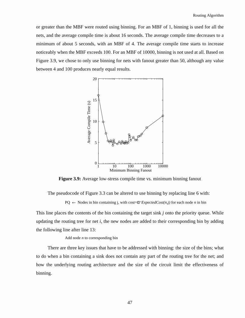
Routing Algorithm
or greater than the MBF were routed using binning. For an MBF of 1, binning is used for all the
nets, and the average compile time is about 16 seconds. The average compile time decreases to a
minimum of about 5 seconds, with an MBF of 4. The average compile time starts to increase
noticeably when the MBF exceeds 100. For an MBF of 10000, binning is not used at all. Based on
Figure 3.9, we chose to only use binning for nets with fanout greater than 50, although any value
between 4 and 100 produces nearly equal results.
The pseudocode of Figure 3.3 can be altered to use binning by replacing line 6 with:
PQ ← Nodes in bin containing j, with cost=α·ExpectedCost(n,j) for each node n in bin
This line places the contents of the bin containing the target sink j onto the priority queue. While
updating the routing tree for net i, the new nodes are added to their corresponding bin by adding
the following line after line 13:
Add node n to corresponding bin
There are three key issues that have to be addressed with binning: the size of the bins; what
to do when a bin containing a sink does not contain any part of the routing tree for the net; and
how the underlying routing architecture and the size of the circuit limit the effectiveness of
binning.
1 10 100 1000 10000Minimum Binning Fanout
0
5
10
15
20
Ave
rage
Com
pile
Tim
e (s
)
Figure 3.9: Average low-stress compile time vs. minimum binning fanout
47

Routing Algorithm
3.3.5.1 Bin Size
If the bin size is too small (in the extreme case the segments in just one logic block tile),
then the quality of the routing degrades since an insufficient amount of the prior route is available
as potential “start points” for the connection to the sink in that bin. If the bin size is too large (in
the extreme case the entire FPGA), then unnecessary segments will be put on the priority queue
and the compile time will increase. Since the average distance between sinks can vary for
different nets, our router computes the bin size based on the span of each net.
Before a net is routed, the average area per sink is calculated as the area of the bounding box
of the net terminals divided by the number of sinks. The bin size for a net is calculated as the
average area per sink multiplied by the bin size scaling factor. The bin size scaling factor
increases the bin size, to increase the probability that a bin containing a sink will also contain a
sufficient amount of the routing tree to make a connection to the sink.
To determine a suitable value for the bin size scaling factor, we routed ten benchmark
circuits (described in Chapter 4) using different values for the bin size scaling factor. Table 3.2
lists the bin size scaling factors, the average minimum track count, the average compile time for
difficult routing problems, and the average compile time for low-stress routing problems.
The average minimum track count is nearly equal for all the different bin size scaling
factors. The average compile time for low-stress problems is nearly constant for scaling factors
greater than or equal to 1.0. The compile time for low-stress problems with a bin size scaling
factor of 0.5 is about 20% higher, on average, compared to the other bin size scaling factors. The
extra time is a result of the bins being too small, so that the bins do not contain enough of the
routing tree to allow a connection to a sink to be found quickly.
Table 3.2: Compile times for different bin size scaling factors
Bin SizeScaling Factor
Geometric AverageMinimum Track
Count
Geometric AverageDifficult
Compile Time (s)
Geometric AverageLow-Stress
Compile Time (s)
0.5 13.6 114.5 6.6
1.0 13.6 81.8 5.4
4.0 13.7 94.5 5.4
9.0 13.7 122.8 5.6
48

Routing Algorithm
For the difficult routing problems, the bin size scaling factor of 1.0 produced the fastest
average compile time. For a bin size scaling factor of 0.5, the bins do not contain enough of the
routing tree to allow a connection to a sink to be found quickly. For scaling factors greater than
1.0, each bin contains much more of the routing tree than required make quick connections. Based
on the results in Table 3.2, we chose to use a bin size scaling factor of 1.0.
3.3.5.2 Empty Bins
If the bin containing a sink does not contain any part of the route so far, then the portions of
the net in its eight neighbouring bins are added to the priority queue. The neighbouring bins may
contain parts of the route relatively close to the target sink. If the neighbouring bins are also
empty, then the entire pre-existing routing tree is placed on the priority queue. In the best case for
an FPGA containing N logic blocks and a net with N sinks, if every sink could be routed using
just the routing in the bin containing the sink, the run-time complexity for the net would be
reduced by a factor of N to O(NlogN). This is assuming that the entire routing tree never has to be
placed back onto the priority queue. In reality, the routing tree will have to be placed back onto the
priority queue at least a few times, so we expect the behaviour to be somewhere in between
O(NlogN) and O(N2logN).
3.3.5.3 Routing Architecture and Circuit Size Dependence
For the simple architecture, which contains only unit-length track segments, we found
binning to be highly effective for reducing the compile time. Through experimentation with
binning, we found that the low-stress compile time improved by 50% on average, compared to
just using a directed search without binning.
Using the same circuits with our 4000X-like architecture, we found that binning was no
longer effective for the following two reasons:
1. By packing a circuit into an architecture containing a logic block with four 4-LUTs, the
number of pins on the highest fanout net is reduced by up to four times, compared to a
logic block with one 4-LUT. Also, the area that the highest fanout net can cover is
reduced by four times. In total, routing the highest fanout net using the 4000X-like archi-
tecture is approximately one sixteenth as difficult compared routing the same net using
the simple architecture. Figure 3.10 shows the minimum binning fanout (MBF) versus
49

Routing Algorithm
compile time for two circuits, for the simple architecture. The smaller circuit, spla,
shows almost no improvement in compile across the range of MBFs. The bigger circuit,
clma, shows a speedup of about 3 times for the range of MBFs from 1 to 400, compared
to not binning any nets (MBF of 1000). Therefore we can conclude that the effectiveness
of binning depends on the size of the routing problem.
2. The second reason that binning is not effective is due to the segmented routing architec-
ture of the 4000X-like architecture. The simple architecture contains just single-length
segments, which fit into exactly one bin. The 4000X-like architecture contains various
length segments, which do not always fit into exactly one bin. For example, a long-length
track segment may cross 10 bin boundaries. After placing the contents of a bin back on
the priority queue, if the router decides to expand a long-length segment, then all of rout-
ing resources attached to the long-length segment must be placed on the priority queue.
Compared to a single-length track segment, a long-length track segment is attached to
many more routing resources, requiring much more time to expand all of the neighbour-
ing resources.
We tried routing circuits on the 4000X-like architecture with the long-length segments
replaced by quad-length segments, and still found binning to be ineffective. The reduction in the
size of the problem appears to be the dominating factor. For this work the largest available
Figure 3.10: Low-stress compile time vs. minimum binning fanout for circuits spla and clma
1 10 100 1000 10000Minimum Binning Fanout (MBF)
0
20
40
60C
ompi
le T
ime
(s)
spla (3690 logic blocks)clma (8383 logic blocks)
50

Routing Algorithm
benchmark circuit contained about 20,000 4-LUTs. For even larger benchmark circuits (more
than 100,000 4-LUTs) binning should once again prove an effective way to reduce the compile
time.
3.4 Circuit Delay Enhancements
The enhancements described in the previous section were principally designed to improve
the compile time, although the net ordering and sink ordering also improved the circuit delay. In
this section we describe enhancements to the base algorithm designed specifically to improve the
circuit delay. These enhancements were tested only with the 4000X-like architecture, since it
contains a segmented routing architecture and a realistic delay model.
Many of the routing algorithms described in Chapter 2 are completely routability-driven--
they do not make any attempt to optimize circuit delay. The problem with completely ignoring
delay is that the resulting circuit delays can be extremely large. For example, in comparing the
routability-driven VPR router to the timing-driven VPR router, the circuit delays for 20 MCNC
circuits were 1.5 to 5 times worse for the routability-driven router [33]. At the other extreme are
fully path-based timing-driven routers, such as the timing-driven VPR router, that use full path-
based timing analysis to optimize circuit delay when routing circuits. The timing-driven VPR
router requires a number of iterations (typically 6 to 10) for nets to successfully negotiate for the
use of timing critical resources (even for low-stress routing problems), which leads to long
compile times.
A middle ground, alternative approach is a net-based (as opposed to a path-based) approach.
Here we simply work to ensure that no net has an overly long delay. We term this kind of
approach “timing-aware”, as opposed to fully path-based timing driven. While a timing-aware
approach may not be able to achieve as high-quality circuit delays as those of a timing-driven
router, the circuit delays will be significantly improved over purely routability-driven routers.
In the next two sections we describe two enhancements to the new high-speed routing
algorithm to make it a timing-aware algorithm.
3.4.1 Switch Counting
The most common way in which delay is built up in a net is by connecting a large number
of pass transistor switches in series, since the delay through pass transistors grows quadratically
51

Routing Algorithm
as the number of pass transistors increases [50]. The delay of a net can be improved by avoiding
long sequences of pass transistors and using some buffers instead, since the delay through a
number of buffers grows linearly [50].
Figure 3.12 shows two examples for routing a two-terminal net using a mixture of pass
transistor and buffered switches. Using the Elmore delay model, the delay of the net in Figure
3.12 (a) is 1.875 ns. If one of the pass transistor switches is replaced by a buffer, as shown in
Figure 3.12 (b), then the delay decreases to 1.125ns.
One way in which long sequences of pass transistor switches can be avoided is by counting
the number of pass transistors used to reach a particular routing resource and adding the count
into the cost function used by the router in Equation (3.1). When the number of pass transistors
grows large, the cost of the current path will become very expensive, causing the router to try to
find a path that uses a buffered resource. The number of pass transistors that are in a sequence is
squared, like the Elmore delay, because this is more realistic than simply counting pass
transistors.
Figure 3.12 shows an example of how the switch count is calculated. Each sequence of pass
transistor switches, separated by at least one buffer, is counted and squared. We define
SwitchCount(n) as the sum of the number of pass transistors in each sequence squared, used to
reach node n
We add the SwitchCount to Equation (3.1) as:
(3.4)
where β is the switch count weight. β is between 0 and 1 and controls how many pass transistors
in a series the router will tolerate before trying an alternative route. With a β of 0, the router com-
pletely ignores switch counting, while a β of 1 causes the router to try and avoid even short series
Source Sink
Figure 3.11: Examples of routing use pass transistor and buffered switches
Source Sink
(a) Elmore Delay = 1.875 ns
(b) Elmore Delay = 1.125 ns
Rpass = 500 ΩCwire = 250 fFTbuff = 125 psRbuff = 500 Ω
TotalCost n( ) PathCost n( ) α ExpectedCost n j,( ) β SwitchCount n( )⋅+⋅+=
52

Routing Algorithm
of pass transistors by trying to use more buffered resources. A large value for β will also cause an
increase in the compile time, because the SwitchCount factor in Equation (3.4) will start to domi-
nate the directed search, and more time is spent back-tracking to search for buffered resources.
An example of the effect of the switch count is shown in Figure 3.13. In this example we
use the cost function given in Equation (3.4) with α = 1.0 and β = 0.2 for simplicity. The net being
routed contains four sinks, and the first three sinks have already been routed using double-length
segments, which are connected using pass transistor switches. When trying to connect to the
fourth sink, there are two choices: use another double-length segment (shown in grey); or use a
quad-length segment originating from the source of the net. In this example, the router will
choose the quad-length segment, because the SwitchCount has made the cost of choosing the
double-length segment higher. While choosing the quad-length segment may not be as good for
overall wirelength, it is a necessary choice for reducing the delay of the net.
To determine the best value for the switch count weight, β, we routed a number of
benchmark circuits using values of β between 0.0 and 1.0. We measured the average compile time
and circuit delay for low-stress and difficult routing problems.
Source node n
SwitchCount(n) = 22 + 32 +12 = 14
Figure 3.12: An example of counting pass transistor switches
sink
source
1
2 3 4TotalCost = 1 + 0 + 0.2*32 = 2.8
cost = 1 + 1 + 0 = 2.0
Figure 3.13: Example of SwichCount
= pass transistor switch
PathCost
ExpectedCost
SwitchCount
53

Routing Algorithm
Figure 3.14 (a) shows a plot of the average compile time and circuit delay versus β, for low-
stress routing problems. The compile time for low-stress problems increases as the value of β
increases. As β increases, the router tries increasingly harder to find paths with fewer pass
transistor switches, requiring more compile time. The circuit delay for low-stress problems is
highest for a β value of 0.0, since the router does not pay any attention to minimizing the use of
pass transistor switches. For any value of β greater than 0.0 the circuit delay is near its minimum;
since there is little routing congestion, the router has an easy time avoiding the use of long series
of pass transistor switches.
Figure 3.14 (b) shows a plot of the average compile time and circuit delay versus β, for
difficult routing problems. The compile time for difficult problems increases as the value of β
increases, again due to the increasing effort by the router to find paths with fewer pass transistor
switches. The circuit delay for difficult problems is fairly large for a β value of 0.0, since the
router does not pay any attention to minimizing the use of pass transistor switches. For any values
of β between 0.01 and 0.4, the circuit delay is near its minimum value. The average circuit delay
starts to increase significantly for values of β greater than 0.4. A large β value causes the router to
use up most of the fast routing resources for the nets routed first; this makes it difficult to route the
remaining nets without using a large number of pass transistor switches, since the routing
problems are difficult and there is a limited number of buffered routing resources.
Given all of the data for both low-stress and difficult routing problems, we chose to use a
switch count weight of 0.1 for the 4000X-like architecture.
Overall, through experimentation on the 4000X-like architecture, just using switch counting
improved the circuit delay for difficult problems by an average of 18%, compared to not using
switch counting. For low-stress problems, the circuit delay improved by an average of 12%,
compared to not using switch counting. The extra expansion operations required by switch
counting increased the compile time by an average of 96% for difficult problems and by an
average of 47% for low-stress problems, compared to not using switch counting.
3.4.2 Track Segment Utilization
Besides avoiding long chains of pass transistor switches, another source of delay in routing
is caused by using the incorrect length of track segments to reach a sink. Utilization is defined as
54

Routing Algorithm
the length of a track segment that is actually required in making a connection divided by the total
length of the track segment [51].
If a sink lies just one logic block away from the source, then using a long-length segment
will result in extra delay for that net. Conversely, if a sink lies on the opposite side of the FPGA
from the source, then using single-length segments to go all the way across the FPGA will also
result in extra delay for the net. In both these cases, track segments are used improperly and
unnecessary delay is added to the connection. The switch counting enhancement already ensures
that short unbuffered track segments are avoided for long connections. But, since circuits usually
contain many short low-fanout connections, it is also important to choose segments to go short
distances appropriately.
Recall from Equation (2.4), that the base cost is the expense for using a routing resource.
For our simple architecture, since all of the track segments are unit length, utilization is not an
issue. We use the same base costs as VPR for the simple architecture, as shown in Table 3.3.
(Recall that the input pin has a slightly lower base cost, so that the router will expand input pins
before other routing resources.) For an FPGA with a segmented routing architecture, having less
expensive base costs for shorter segments ensures that the shortest segment will be chosen when
there are multiple segments that reach the target sink, which is equivalent to the concept of
Figure 3.14: Average compile time vs. β, (a) low-stress routing problems, (b) difficult routing problems, for 4000X-like architecture
(a) (b)
0.0 0.2 0.4 0.6 0.8 1.0Switch Count Weight (β)
10
20
30
40
Ave
rage
Com
pile
Tim
e (s
)Compile Time
80
90
100
110
Ave
rage
Cir
cuit
Del
ay (
ns)
Circuit Delay
0.0 0.2 0.4 0.6 0.8 1.0Switch Count Weight (β)
0
200
400
600
800
Ave
rage
Com
pile
Tim
e (s
)
Compile Time
100
110
120
130
Ave
rage
Cir
cuit
Del
ay (
ns)
Circuit Delay
55

Routing Algorithm
utilization in the SEGA router [15]. For the 4000X-like architecture, we set the base costs of
shorter track segments to slightly smaller values than the base costs of longer track segments, as
listed in Table 3.3.
An example of the effect of different base costs is shown in Figure 3.15. In this example we
are trying to route from the source of a net to a target sink that lies two units away. We could use
two single-length segments to reach the target. Alternatively, we could reach the target with just
one double-length, quad-length, or long-length segment. In this case, it makes the most sense to
use the double-length segment since it is does not waste any part of a wire and reaches the sink
directly. If the quad-length or long-length segment were chosen, then at least half of a track
segment would be wasted. Since the cost of the double-length segment is the cheapest, it will be
chosen. If all the segments had a base cost of 1.0, then any of the segments could be chosen to
reach the target sink.
Through experimentation, we found that for difficult routing problems, the circuit delay
improved by an average of 17%, compared to not using the segment utilization enhancement.
Table 3.3: Base cost of different routing resources
ResourceSimple
Architecture[34]
4000X-likeArchitecture
single-length track segment 1.00 0.97
double-length track segment N/A 0.98
quad-length track segment N/A 0.99
long-length track segment N/A 1.00
logic block output pin 1.00 1.00
logic block input pin 0.95 0.95
source 1.00 1.00
sink 0 0
Total Distance = 2Source
S TTarget
Single
Double
Quad
Long
Cost=0.98
Cost=0.99
Cost=1.00
Figure 3.15: Example of the affect of different base costs
Cost=2*0.97=1.94
56

Routing Algorithm
Similarly, for low-stress routing problems, the circuit delay improved by an average of 5%,
compared to not using the segment utilization enhancement.
3.5 Summary of Enhancement Effectiveness
Throughout this chapter, we have described the results of experiments to measure the
effectiveness of each of the routing algorithm enhancements. In this section, we provide a
summary of all of the enhancement experiments for both architectures.
3.5.1 Simple Architecture
In this section, we summarize the effectiveness of the directed search and binning. We
compare the high-speed router to the routability-driven VPR router, using the simple architecture.
Recall from Section 3.3.5, that binning was only effective for reducing the compile time using the
simple architecture.
We made measurements using the routability-driven VPR router, the high-speed router
using only the directed search, and the high-speed router using the directed search and binning.
We ran all of the routers using the fast routing schedule. In Table 3.4 we list each of the routers,
the average minimum track count, the routing time for difficult problems, and the average routing
time for low-stress problems. (Note that Wmin is defined as the minimum track count required to
route a circuit, we make a routing problem low-stress by using 30% more tracks than Wmin.)
None of the enhancements significantly increased the average minimum track count over
the routability-driven VPR router. For the difficult routing problems, using only a directed search
produced a 5.6 times speedup, on average, compared to VPR. Binning resulted in another 1.6
times speedup, on average, for the difficult routing problems. For the low-stress routing problems,
using only a directed search produced nearly a 50 times speedup, on average, compared to VPR.
The addition of binning provided another 1.8 times speedup, on average.
3.5.2 4000X-Like Architecture
In this section, we summarize the effectiveness of the rest of the algorithm enhancements.
We compare the relative effectiveness of using different combinations of the enhancements. For
57

Routing Algorithm
these measurements we used the 4000X-like architecture, since all of the enhancements in
Table 3.5 affect the circuit delay.
Table 3.5 lists all of the possible combinations of enhancements (in which X = enabled, --
= disabled) and the experimental results for the enhancements. For each combination of
enhancements, we measured the average minimum track count, the average compile time for
difficult and low-stress routing problems, and the average circuit delay for difficult and low-stress
routing problems.
The highlighted rows mark where just one enhancement is enabled (these are the results
presented for each enhancement earlier in this chapter). The first observation is that the minimum
track count is relatively constant across all combinations of enhancements, varying by just 5%.
An interesting combination of enhancements is the combination of net ordering and sink
ordering (line 4). The combination of these enhancements improved the difficult compile time and
the low stress circuit delays more than using each of these enhancements separately. Similarly, the
combination of switch counting and segment utilization (line 13) improved the difficult and low-
stress circuit delays more, compared to using each of these enhancements separately.
Another observation from Table 3.5 is that for all the combinations of enhancements where
switch counting is enabled, the compile time is up to twice as long for both low-stress and difficult
routing problems, compared to when switch counting is disabled. For all of these cases the circuit
delay is improved when switch counting is enabled. For example, the average compile for difficult
Table 3.4: Effectiveness of directed search and binning for simple architecture
Difficult Routing Problems(Wmin tracks)
Low Stress Problems(Wmin + 30% tracks)
Algorithm
GeometricAverage
MinimumTrack Count
GeometricAverage
Compile Time (s)
Speedupover VPR
GeometricAverage
Compile Time (s)
Speedupover VPR
Routability-DrivenVPR Router
(Breadth-First Search)
13.8 837 -- 435 --
High-Speed Routerwith Directed Search
14.0 150 5.6 9 48.3
High-Speed Routerwith Directed Search
and Binning
14.0 94 8.9 5 87.0
58

Routing Algorithm
routing problems is 246.5 seconds in row 8 and 486.7 seconds in row 16. The average circuit
delay improves from 160.4 ns to 132.9 ns.
Overall, having all the enhancements enabled (row 16) produced the best results on average
across both difficult and low stress routing cases. Other combinations of enhancements were
slightly better for some of the measured compile times and circuit delays, but did not provide as
good results across all the measurements.
Table 3.5: Effectiveness of enhancements for 4000X-like architecture (X enabled, -- disabled)
Algorithm EnhancementAverage Compile
Time (s)Average
Circuit Delay (ns)
SwitchCounting
Util-ization
NetOrdering
SinkOrdering
AverageMinimum
Track CountDifficult
Low-Stress
DifficultLow-Stress
1 -- -- -- -- 51.5 320.5 15.2 194.5 113.1
2 -- -- -- X 52.1 253.8 12.0 174.9 113.6
3 -- -- X -- 50.6 246.5 17.0 172.7 99.2
4 -- -- X X 51.0 235.9 15.7 173.6 95.7
5 -- X -- -- 50.8 274.9 12.7 162.2 107.5
6 -- X -- X 51.4 206.4 11.7 168.1 109.3
7 -- X X -- 50.4 264.3 15.8 135.2 97.6
8 -- X X X 50.3 246.5 15.7 139.5 102.7
9 X -- -- -- 52.0 629.1 22.4 160.4 99.9
10 X -- -- X 52.2 619.2 21.2 145.8 96.9
11 X -- X -- 50.5 505.3 23.2 127.5 94.2
12 X -- X X 50.6 539.0 21.3 129.6 90.0
13 X X -- -- 51.5 609.1 22.0 148.5 97.4
14 X X -- X 52.6 405.4 18.7 146.6 96.1
15 X X X -- 50.3 480.7 22.5 128.0 93.0
16 X X X X 50.5 486.7 19.7 132.9 89.9
59

Routing Algorithm
3.6 Summary
In this chapter, we described enhancements to the basic routing algorithm aimed at
increasing the execution speed and reducing the circuit delay. The enhancements were: directed
search, fast routing schedule, net ordering, sink ordering, binning, switch counting, and segment
utilization. We also presented a summary of the effectiveness of all the routing algorithm
enhancements.
In the next, chapter we present experimental results for the new high-speed timing-aware
router.
60

Experimental Results
Chapter 4
Experimental Results
In this chapter, we present the results of experiments run to measure the ability to minimize
track count, execution speed, and circuit delay of the new high-speed timing-aware routing
algorithm. We start by describing the benchmark circuits used and then present the results from
experiments run using the simple FPGA architecture. We then present results from experiments
run using the 4000X-like architecture.
4.1 Benchmark Circuits
To experiment with the new high-speed router, we required a set of large benchmark
circuits. Unfortunately, very large circuits are difficult to obtain, but we did manage to collect 10
suitable circuits. The benchmark circuits are listed in Table 4.1. The circuit sizes range from 3556
4-LUTs up to 19,600 4-LUTs. Eight of the circuits are the largest circuits from the MCNC suite
[2]. The other two circuits were created using the synthetic benchmark circuit generator (GEN)
[45]. Although the latter circuits are actually somewhat more difficult than real circuits, we
believe they are perfectly reasonable test cases for the compile time issue.
Each of the MCNC circuits was synthesized with the SIS [46] package and technology
mapped using Flowmap [47]. The technology-mapped circuits were then packed into logic blocks
using VPACK [34]. The synthetic circuits were only packed into logic blocks using VPACK as
they were generated in technology-mapped form. Each circuit was then placed using VPR.1
1. The VPR placement tool was run using the “-fast” option that speeds up the execution time by about 10 times, with 5% to 10% quality degradation.
61

Experimental Results
4.2 Simple Architecture Experiments
In this section, we use the simple FPGA architecture to compare the ability to minimize
track count and execution speed of the new high-speed router to the routability-driven VPR router.
These experiments also serve to compare the directed search used by the new router to the
breadth-first search used by the routability-driven VPR router.
For the high-speed router, all of the compile time enhancements were enabled (directed
search, fast routing schedule, net ordering, sink ordering, and binning). The routability-driven
VPR router was also run in its fastest mode, using the fast routing schedule.
4.2.1 Quality: Minimum Track Count
In the first experiment, we compare the quality of the high-speed router to the routability-
driven VPR router, by comparing the minimum track count needed to successfully route each of
the benchmark circuits.
To measure the minimum track count for each circuit, we started with a very low track
count and increased the track count by one track until the circuit could be routed. Table 4.2 lists
the minimum track counts for each of the benchmark circuits, using both routers. Recall that we
define Wmin as the minimum track count required by the high-speed router to route a circuit. The
Table 4.1: Benchmark circuits
Circuit Source # 4-LUTs
beast16k GEN 15680
beast20k GEN 19600
clma MCNC 8383
elliptic MCNC 3604
ex1010 MCNC 4598
frisc MCNC 3556
pdc MCNC 4575
s38417 MCNC 6406
s38584.1 MCNC 6447
spla MCNC 3690
62

Experimental Results
new high-speed router is clearly of high quality, since it achieved the same track count as VPR on
9 out of 10 circuits and only required one extra track for the other circuit.
4.2.2 Compile Time
In this section, we compare the compile time of the high-speed router to that of the
routability-driven VPR router.
Since the compile time of any router is strongly affected by the difficulty of the routing
problem, we will vary the difficulty of the problem. Recall that we define WFPGA as the number of
tracks per channel in the target FPGA. The difficulty of the routing problem is controlled by using
different values of WFPGA--the closer WFPGA is to the Wmin of the circuit, the harder the routing
problem gets.
We routed each of the benchmark circuits using both the new high-speed router and the
routability-driven VPR router. For each circuit we used track counts ranging from Wmin up to
Wmin + 20% track per channel. Table 4.3 lists the benchmark circuits, the compile times for both
routers, and the speedup of the high-speed router over VPR. All of the compile times were
measured on a 300 MHz UltraSPARC 3200 with 1 GByte of memory, and do not include the time
Table 4.2: Minimum track counts for the simple architecture
CircuitRoutability-Driven VPR
Min.Track Count
High-Speed RouterMin. Track Count
(Wmin)
%Difference
beast16k 23 23 0.0
beast20k 29 29 0.0
clma 12 12 0.0
elliptic 12 12 0.0
ex1010 13 14 7.7
frisc 12 12 0.0
pdc 16 16 0.0
s38417 8 8 0.0
s38584.1 8 8 0.0
spla 14 14 0.0
Total 148 148 0.0
63

Experimental Results
to parse the netlist and generate the routing graph. For the largest circuit the parse and graph
generation time is 20 seconds. The largest circuit, beast20k, requires 200 MBytes of memory.
At Wmin tracks per channel, the high-speed router is 6.9 times faster, on average, than the
routability-driven VPR router. At these track counts, the routing problems are difficult, bordering
on impossible to route. The large amount of congestion slows down the directed search
considerably. For the two largest circuits, beast16k and beast20k, the high-speed router is over 25
times faster than the routability-driven VPR router, although the high-speed router still requires
several minutes to compile each circuit. For the rest of the circuits, the high-speed router is
between 1.6 and 19.8 times faster than VPR.
As WFPGA increases, the routing problems become significantly easier since there is less
routing congestion. The directed search is more efficient at routing nets when there is less
congestion. The average compile time of both routers decreases, but the high-speed router
achieves a much greater speedup compared to VPR. At Wmin + 20%, the high-speed router is 58
Table 4.3: Compile times for simple architecture
WFPGA Wmin Wmin + 10% Wmin + 20%
CircuitVPR
Time (s)
High-SpeedRouter
Time (s)
Speedup
VPRTime (s)
High-SpeedRouter
Time (s)
Speedup
VPRTime (s)
High-SpeedRouter
Time (s)
Speedup
beast16k 23761 183 129.8 7079 42 168.5 5522 26 212.4
beast20k 19678 775 25.4 16321 110 148.4 13142 68 193.3
clma 1264 483 2.6 2029 40 50.7 840 18 46.7
elliptic 241 29 8.3 133 8 16.6 198 4 49.5
ex1010 316 16 19.8 206 4 51.5 109 2 54.5
frisc 262 163 1.6 257 11 23.4 190 4 47.5
pdc 639 353 1.8 497 22 22.6 581 7 83.0
s38417 330 59 5.6 193 27 7.1 142 8 17.8
s38584.1 338 86 3.9 81 26 3.1 88 10 8.8
spla 326 78 4.2 255 9 28.3 259 2 129.5
GeometricAverage
837 122 6.9 564 20 28.2 465 8 58.1
64

Experimental Results
times faster on average compared to VPR. Notice that for the largest MCNC circuit, clma, the
high-speed router is 46.7 times faster than VPR. For the largest circuit, beast20k, the high-speed
router is 193.3 times faster than VPR. Although not shown in the table, with Wmin + 30% extra
tracks, the beast20k can be routed in only 20 seconds by the high-speed router.
It is instructive to observe how the compile time of the high-speed router changes as the
available track count, WFPGA, increases. Figure 4.1 plots the routing time for the high-speed
router and VPR versus the number of tracks available, for the 8383 logic block circuit clma. It is
clear that once there are sufficient tracks the new router completely routes the circuit in about 6
seconds, independent of the number of tracks. The speedup as WFPGA increases comes from two
factors: fewer routing iterations (eventually, only 1) are needed to resolve congestion; and the
directed search can more rapidly route each net when there is little routing congestion to detour
around. Observe that the routability-driven VPR router takes a great deal more time, and the time
increases as WFPGA increases (for large WFPGA) because of the breadth-first search nature of the
VPR router.
Now that we have demonstrated the high quality and fast execution speed for the high-speed
router targeting the simple architecture, in the next section we present the results from
experiments run using the 4000X-like architecture.
Figure 4.1: Compile time vs. available tracks for clma (8383 logic blocks)
10 15 20 25Tracks per Channel (WFPGA)
0
1000
2000
3000
Com
pile
Tim
e (s
)
High-Speed RouterRoutability-Driven VPR Router
65

Experimental Results
4.3 4000X-Like Architecture Experiments
In this section, we use the 4000X-like FPGA architecture to compare the ability to
minimize track count, execution speed, and circuit delay of the new high-speed router to the
timing-driven VPR router. Our main reasons for carrying out these experiments were: first, to
measure the performance of the new high-speed router targeting a realistic FPGA architecture;
and second, to the compare the high-speed router to the timing-driven VPR router.
For the high-speed router, all of the compile time and circuit delay enhancements were
enabled. Recall from Chapter 3, that the two circuit delay enhancements were switch counting
and track segment utilization.
4.3.1 Quality: Minimum Track Count
In the first experiment, we compare the quality of the high-speed router to the timing-driven
VPR router, by comparing the minimum track count needed to successfully route each of the
benchmark circuits.
The results were obtained using the same procedure described for the simple architecture in
Section 4.2.1. Table 4.4 list the benchmark circuits, the minimum track count for each router, and
the percent difference. The high-speed router requires an average of 11% more tracks per channel,
compared to the timing-driven VPR router.
There are many differences between the high-speed timing-aware router and the timing-
driven VPR router, so it is unclear exactly why our router is not able to route circuits as efficiently
as VPR. One key difference between the two routers is the trade-off between routability and delay.
Recall from Section 2.3.4.5 that the timing-driven VPR router assigns a criticality to each net
based on the slack of the net. Nets that are non-critical pay more attention to routability, while
nets that are critical pay more attention to minimizing delay. The high-speed router uses a fixed
trade-off between routability and delay, so that all of the nets are routed with the same attention
given to routability and delay; nets that are non-critical are not necessarily routed with the shortest
wirelength.
66

Experimental Results
4.3.2 Compile Time
In this section, we compare the compile time of the high-speed router to the compile time of
the timing-driven VPR router. Similar to Section 4.2.2, we measured the compile times over a
range of track counts, ranging from Wmin up to Wmin + 20% tracks per channel.
Table 4.5 lists the benchmark circuits, the compile time for the timing-driven VPR router
and the high-speed router, and the speedup of the high-speed router over VPR. Execution times
were again measured on a 300 MHz UltraSPARC.
At Wmin tracks, the high-speed router requires an average of 2.7 times more compile time
than the timing-driven VPR router. At these track counts, our router is operating on the edge of
routability for all of the circuits, while VPR is operating closer to the low-stress range. At
Wmin + 10% tracks, the high-speed router is 2.5 times faster, on average, compared to VPR. At
Wmin + 20%, the high-speed router is 5.2 times faster, on average, compared to VPR.
It is interesting to note that the timing-driven VPR router is significantly faster compared to
the routability-driven VPR router (see Section 4.2.2), since the timing-driven VPR router uses a
directed search. The high-speed routing algorithm is still somewhat faster than the timing-driven
Table 4.4: Minimum track counts for 4000X-like architecture
CircuitVPR Min
TrackCount
High-SpeedRouter
Min. TrackCount (Wmin)
%difference
beast16k 71 79 11.3
beast20k 84 92 9.5
clma 47 53 10.6
elliptic 38 42 10.5
ex1010 39 42 7.7
frisc 37 39 5.4
pdc 55 63 14.5
s38417 32 36 12.5
s38584.1 28 32 14.3
spla 51 57 11.8
Total 482 535 11.0
67

Experimental Results
VPR router, since the high-speed router tries more aggressively to route a circuit in just one
iteration. The timing-driven VPR router tries to balance routability and circuit delay over a
number of iterations, typically requiring 6 to 10 iterations, even for low-stress routing problems.
4.3.3 Quality: Circuit Delay
Now that we have established the execution speed for the new high-speed router, we now
measure the ability of the high-speed router to minimize circuit delay compared to the timing-
driven VPR router. We once again use track counts ranging from Wmin up to Wmin + 20% tracks
per channel.
Table 4.6 lists the benchmark circuits, the circuit delays for the high-speed router and the
timing-driven VPR router, and the percentage difference between the two routers. The circuit
delays were calculated using the timing analyzer of VPR.
At Wmin tracks, the high-speed router has 60% more circuit delay, on average, compared to
the timing-driven VPR router. Since we are routing at the very minimum track count for each
Table 4.5: Compile times for 4000X-like architecture
WFPGA Wmin Wmin + 10% Wmin + 20%
CircuitVPR
Time (s)
HighSpeedRouter
Time (s)
Speedup
VPRTime (s)
HighSpeedRouter
Time (s)
Speedup
VPRTime (s)
HighSpeedRouter
Time (s)
Speedup
beast16k 515 1235 0.4 551 141 3.9 378 70 5.4
beast20k 918 2137 0.4 839 233 3.6 815 127 6.4
clma 246 407 0.6 183 42 4.4 257 28 9.2
elliptic 79 199 0.4 53 38 1.4 51 19 2.7
ex1010 110 280 0.4 93 52 1.8 84 15 5.6
frisc 65 169 0.4 53 35 1.5 56 10 5.6
pdc 159 610 0.3 153 33 4.6 156 20 7.8
s38417 100 196 0.5 81 58 1.4 77 45 1.7
s38584.1 75 277 0.3 46 34 1.4 55 12 4.6
spla 129 570 0.2 110 24 4.6 109 13 8.4
GeometricAverage
159 425 0.4 130 52 2.5 130 25 5.2
68

Experimental Results
circuit, there is so much congestion that the router is forced to route many of the nets using paths
with large delays.
As the track count increases, the circuit delay for the high-speed router decreases. At
Wmin + 20% tracks the high-speed router is just 16% worse on average compared to VPR. With
less congestion, the high-speed router is able to effectively reduce the delay caused by long
sequences of pass transistors by using the switch counting enhancement. The segment utilization
enhancement is also effective at reducing the circuit delay by avoiding the use of long segments
for short nets. The delay of the beast20k decreased from 84% worse than VPR at Wmin tracks, to
only 19% worse than VPR at Wmin + 20% tracks.
Now that we have measured the ability to minimize track count, execution speed, and
circuit delay of the high-speed router when all of the compile time and circuit delay enhancements
are enabled, in the next section we demonstrate how the compile time can be further reduced.
Table 4.6: Circuit delays for 4000X-like architecture
WFPGA Wmin Wmin + 10% Wmin + 20%
CircuitVPR
Delay(ns)
HighSpeedRouter Delay
(ns)
%diff.
VPR Delay
(ns)
HighSpeedRouter Delay
(ns)
%diff.
VPR Delay
(ns)
HighSpeedRouter Delay
(ns)
%diff.
beast16k 121 225 86 116 146 26 120 123 3
beast20k 180 332 84 168 194 15 163 194 19
clma 100 135 35 96 115 17 97 121 25
elliptic 77 149 94 63 89 41 62 77 24
ex1010 70 97 39 64 74 16 58 74 28
frisc 87 127 46 80 100 25 83 103 24
pdc 77 98 27 78 82 5 75 88 17
s38417 56 84 50 66 81 23 60 68 13
s38584.1 40 94 135 40 52 30 40 49 23
spla 71 123 73 69 82 19 69 75 9
GeometricAverage
81 133 60 78 95 19 77 91 16
69

Experimental Results
4.3.4 Reducing the Compile Time
Recall from Section 3.5, that when the switch counting enhancement was enabled for the
high-speed router the circuit delay improved by up to an average of 20%, but the compile time
nearly doubled. In this section we measure the affect of disabling the switch counting
enhancement, as the routing problem difficulty changes.
We routed each of benchmark circuits using the high-speed router with all of the
enhancements enabled, the high-speed router with the switch counting enhancement disabled, and
the timing-driven VPR router. Using track counts ranging from Wmin tracks up to Wmin + 30%
extra tracks for each of the benchmark circuits, we measured the compile time and circuit delay
for each circuit. In this section we present the results graphically, as it is instructive to observe
graphically how the compile time and circuit delay of the high-speed timing-aware router changes
as the available track count increases.
Figure 4.2 (a) plots the average compile time for the high-speed router with all the router
enhancements enabled, the high-speed router with switch counting disabled, and the timing-
driven VPR router, versus the percentage extra tracks. At Wmin tracks per channel, the timing-
driven VPR router is faster than both versions of the high-speed router. With just 5% extra tracks
both versions of the high-speed router are faster than VPR. Once there are 10% extra tracks, the
high-speed router with and without switch counting disabled is clearly much faster than VPR. The
speedup as the percentage extra tracks increases comes from two factors: fewer routing iterations
(eventually, only 1) are needed to resolve congestion; and the directed search can more rapidly
route each net when there is little congestion to detour around. Also notice that the high-speed
router with switch counting disabled is always faster than the high-speed router with all the
enhancements enabled.
Observe that the VPR router takes a great deal more compile time, and the time relatively
stays constant as the percentage extra tracks increases. Figure 4.2 (b) gives a close-up view of the
10% to 30% extra track region of Figure 4.2 (a). We observe that at 30% extra tracks, the high-
speed router with all the enhancements enabled requires 20 seconds, on average. The high-speed
router with switch counting disabled requires only 15 seconds, on average.
Figure 4.3 (a) plots the average circuit delay for the high-speed router with all the router
enhancements enabled, the high-speed router with switch counting disabled, and the timing-
driven VPR router, versus the percentage extra tracks. With no extra tracks, both versions of the
70

Experimental Results
high-speed router have a very difficult time minimizing circuit delay, due to the large amount of
routing congestion. As the percentage extra tracks increases, the high-speed router with all the
enhancements enabled is able to reduce the circuit delay, settling to within 20% of VPR, on
average, with just 5% extra tracks. The high-speed router with switch counting disabled always
has at least 35% higher circuit delay than VPR, on average.
If we compare Figure 4.2 (a) and Figure 4.3, we can see that there is a trade-off between
compile time and circuit delay. In situations where circuit delay is not important, the router can be
run with switch counting disabled to obtain the fastest compile time. When circuit delay is
important, the router can be run with the all enhancements enabled, which will improve the circuit
delay by about 20%, requiring up to twice as much compile time, on average, compared to when
switch counting is disabled.
4.4 Summary
In this chapter, we presented the results of experiments run on the simple FPGA
architecture and 4000X-like FPGA architecture. We measured the ability of the high-speed router
0 10 20 30% Extra Tracks
0
100
200
300
400
500
Com
pile
Tim
e (s
econ
ds)
VPRNo Switch CountingAll Enhancements
Figure 4.2: (a) Compile time vs. % extra tracks, (b) Compile time vs. % extra tracks (zoomed)
(a) (b)
10 15 20 25 30% Extra Tracks
0
50
100
150
Com
pile
Tim
e (s
econ
ds)
VPRNo Switch CountingAll Enhancements
71

Experimental Results
to minimize the track count for the two architectures and found that it is excellent for the simple
architecture, but not quite as good for the 4000X-like architecture. We demonstrated the
extremely fast execution time of the high-speed router on large benchmark circuits--the largest
circuit, beast20k, can be compiled in 68 seconds targeting the simple architecture and 127
seconds targeting the 4000X-like architecture (with 20% extra routing resources). We also
demonstrated the ability of the high-speed router to minimize circuit delay; with only 5% extra
routing resources, the average circuit delay was only 20% higher, compared to the timing-driven
VPR router.
In the next chapter we consider two issues in the practical use of a high-speed router.
0 10 20 30% Extra Tracks
60
80
100
120
140
Cir
cuit
Del
ay (
ns)
VPRNo Switch CountingAll Enhancements
Figure 4.3:Circuit delay vs. % extra tracks
(4.1)
72

Practical Issues
Chapter 5
Practical Issues
In this chapter, we consider issues in the practical use of an ultra-fast router. The first issue
is difficulty prediction--detecting early on when a routing problem is impossible or difficult (and
will take a long time to solve). The second issue deals with how to practically reduce the difficulty
of a routing problem in the context of using a real family of FPGAs.
5.1 Difficulty Prediction
When routing a circuit in an FPGA, there may be times when the circuit is difficult or
impossible to route. Existing routers spend a very long time routing difficult circuits and for
impossible problems they can take several hours simply to declare failure. There is almost no
benefit to using an ultra-fast router if the user ever has to wait a long time for a circuit to be routed
(without being warned at the start) or to declare failure.
Therefore, a key aspect of ultra-fast routing is the ability to quickly predict when the routing
problem is very hard or impossible. In both of these cases, it is important to inform the user that
the result will either be a long time coming, or simply isn’t possible to achieve. When a routing
problem is difficult or impossible, the designer has two main options: reduce the amount of logic
in the circuit or move to a larger device.
In this section, we describe an approach for predicting the difficulty of routing a circuit
given the placement of the circuit and information about the target FPGA. This method
presupposes that there is a fast way of generating a placement, which is the subject of related
research [52].
73

Practical Issues
To predict the difficulty of routing a circuit, two pieces of information are required: the
number of tracks per channel in the target FPGA (which is known beforehand), and an estimate of
the minimum track count required to route the circuit. To determine the minimum track count, an
estimate of the total wirelength for the circuit is needed.
5.1.1 Estimating Total Wirelength
We can calculate the total estimated wirelength for a circuit from its placement using the
placement-based wirelength model described in Section 2.4.1. Recall that the wirelength needed
to route a net can be estimated by multiplying the half-perimeter bounding-box wirelength of the
net terminals by the fanout-based correction factor. We can obtain an estimate of the total
wirelength by summing the estimated wirelength for every net.
For the simple FPGA architecture, we found that the correction factors given in RISA for
nets with up to 50 terminals (see Table 2.1) were very accurate. To determine the correction
factors for higher fanout nets, we routed the larger MCNC benchmark circuits ignoring
congestion, and recorded the actual wirelength for each net. By dividing the actual wirelength by
the bounding box half-perimeter wirelength, we obtained average correction factors for nets with
more than 50 terminals. Instead of storing discrete values for all the correction factors for nets
with more than 50 terminals, we fit the data to equations (5.1) and (5.2) using the “least squares
approximation”. C(k) is the correction factor and k is the number of terminals. With these
correction factors, our estimates of total wirelength are within 5% of the actual wirelength for all
of our benchmark circuits. (Note that linearly extrapolating the RISA correction factors led to
estimates of total wirelength that were up to 25% too high.)
(5.1)
(5.2)
For the 4000X-like FPGA architecture, we found that the correction factors from RISA
were too low. This is because the amount of wiring required to route nets is higher for the 4000X-
like architecture, compared to the simple architecture. To improve the correction factors for the
4000X-like architecture, we reran the same experiments used to determined the correction factors
for the simple architecture. For nets of fanout less than 50, we use the correction factors listed in
Table 5.1. For nets with fanout greater than 50, we fit the data to equation (5.3) using the least
squares approximation.
C k( ) 2.6 2–×10 k 1.49 for 50 < k < 85+⋅=
C k( ) 1.8 6–×10 k2 1.1 2–×10 k 2.79 for k 85≥+⋅+⋅–=
74

Practical Issues
(5.3)
By using the fanout-based correction factors we can obtain an estimate of the total
wirelength for a circuit and then calculate the estimated track count.
5.1.2 Estimating Track Count
Using the total estimated wirelength, the estimated track count, Westimate, can be calculated
as:
(5.4)
where N is the total number of logic blocks in the target FPGA and U is the track segment utiliza-
tion. The track segment utilization is the fraction of the total number of track segments in the
FPGA that a router can typically use before congestion prevents some nets from being routed. The
denominator term is the total number of usable channels in the FPGA. By dividing the total esti-
mated wirelength by the number of usable channels, we get the number of tracks required per
channel.
The utilization figure captures elements of the complexity of both routing a particular
FPGA architecture and the circuit being routed on that architecture. This is a complicated
interaction, and it is over-simplified to represent these issues as a constant; however, as explained
below, this works for our purposes.
Table 5.1: Correction factors up to 50 for 4000X-like architecture
FanoutCorrection
FactorFanout
CorrectionFactor
1 1.00 10 2.05
2 1.25 15 2.45
3 1.39 20 2.69
4 1.55 25 3.22
5 1.64 30 3.45
6 1.76 35 3.50
7 1.77 40 3.80
8 1.89 45 4.03
9 1.98 50 4.45
C k( ) 2 2–×10 k 4.4 for k > 50+⋅=
W estimatetotal estimated wirelength
2 N U⋅ ⋅-----------------------------------------------------------------------=
75

Practical Issues
The utilization, U, can be determined experimentally for a router using Equation (5.4) and a
set of benchmark circuits. By using the total estimated wirelength for each circuit and substituting
the actual minimum track count for Westimate, U can be calculated for each circuit.
Table 5.2 lists each of the benchmark circuits from Chapter 4, the size of each circuit, Wmin,
the total estimated wirelength, and the utilization calculated using Equation (5.4). These results
are for the simple FPGA architecture. The values of U range from 0.45 up to 0.60 and the average
value is 0.54. The utilization is always less than 1.0, since it impossible to use all of the routing
resources in an FPGA for routing a circuit. The small variance in the value of U is caused by the
errors in the total estimated wirelength for each circuit. It is important to note that since the values
of U are relatively constant across different circuits, the average value for U can be used for
calculating the estimated track count with Equation (5.4).
Table 5.3 lists the utilization results for the 4000X-like architecture. The values of U range
from 0.69 up to 0.81 and the average value is 0.74. Notice that the average utilization is higher for
the 4000X-like architecture, compared to the simple architecture. Certain features of the 4000X-
like architecture are more flexible, compared to the simple architecture. With a more flexible
architecture, it is easier to use more of the total routing resources, resulting in an increased
Table 5.2: Utilization for simple architecture
Circuit# LogicBlocks
WminTotal Estimated
WirelengthUtilization (U)
beast16k 15680 23 404619 0.56
beast20k 19600 29 615294 0.54
clma 8383 12 120360 0.60
elliptic 3604 12 42169 0.49
ex1010 4598 14 57599 0.45
frisc 3556 12 49132 0.58
pdc 4575 16 81767 0.56
s38417 6406 8 57262 0.56
s38584.1 6447 8 53154 0.52
spla 3690 14 56051 0.54
Average 0.54
76

Practical Issues
utilization figure. One might surmise that the simple architecture, with only single-length track
segments and a non-planar switch box, would be more flexible than the 4000X-like architecture,
with its segmented routing architecture. The method for estimating total wirelength already
accounts for the difference in segment lengths, since the bounding-box correction factors were
determined separately for each architecture. In addition, there are two features of the 4000X-like
architecture that make it more flexible than the simple architecture. The 4000X-like architecture
contains larger logic blocks with more pins, compared to the simple architecture, so there is more
flexibility in choosing input and output pins. The 4000X-like architecture also contains more
tracks per channel, compared to the simple architecture, for routing the equivalent circuit. It is
easier to route a circuit when the FPGA contains larger channels; a larger channel is more flexible,
allowing more nets to be packed into the channel. For example, if two tracks are wasted in a
channel containing ten tracks in total, then only 80% of the channel is utilized. If two tracks are
wasted in a channel containing forty tracks in total, then 95% of the channel is utilized.
5.1.3 Difficulty Classification
Now that we have a method for calculating the estimated track count for a circuit, we need a
method for predicting the difficulty of routing a circuit. Clearly, the difficulty of routing a circuit
Table 5.3: Utilization for 4000X-like architecture
Circuit# LogicBlocks
WminTotal Estimated
WirelengthUtilization (U)
beast16k 3937 79 451079 0.73
beast20k 4929 92 649044 0.72
clma 2121 53 156277 0.70
elliptic 903 42 57592 0.76
ex1010 1191 42 74896 0.75
frisc 892 39 56235 0.81
pdc 1194 63 103132 0.69
s38417 1604 36 89670 0.78
s38584.1 1612 32 81558 0.79
spla 953 57 74858 0.69
Average 0.74
77

Practical Issues
is a function of the estimated track count for the circuit and the number of tracks in the target
FPGA; recall that we call the number of tracks in the FPGA, WFPGA.
When the number of tracks in the FPGA is less than the estimated number of tracks required
by the circuit, we classify the problem as impossible. Recall from Figure 4.1 in Chapter 4, that as
the track count is increased from the minimum required by a circuit, the compile time for the
high-speed router quickly decreases to a near minimum value with only ten percent extra tracks
per channel. Therefore, we classify a problem as difficult if the target FPGA has less than the
minimum track count required by the circuit plus ten percent. If the FPGA has more tracks per
channel than the minimum track count required by the circuit plus ten percent, we classify the
problem as low-stress. Table 5.4 summarizes the three classifications.
5.1.4 Demonstrations of Difficulty Prediction
To test the difficulty prediction scheme, we use the ten benchmark circuits from Chapter 4.
We executed the predictor for each circuit to determine the estimated track count using Equation
(5.4) after placement. Westimate requires less than less than one second to calculate for the largest
benchmark circuit, providing the user with feedback on the problem classification very quickly.
Table 5.5 lists the actual minimum track count (as determined by the router) and the estimated
track count for each benchmark circuit for the simple architecture. The last column in Table 5.5
shows the difference between Westimate and Wmin. For nine of the circuits, the estimates are within
±1 track per channel. For the remaining circuit, the estimate is two tracks per channel lower than
the actual minimum track count.
Table 5.6 lists the actual minimum track count and estimated minimum track count for each
of the benchmark circuits, using the 4000X-like architecture. The estimates are accurate to within
±4 track per channel or ±10% of the actual minimum track counts.
Table 5.4: Definition of routing classes
ClassificationTypical Range of Tracks
Per Channel in FPGA
Impossible WFPGA< Westimate
Difficult Westimate ≤ WFPGA< 1.1Westimate
Low-Stress WFPGA ≥ 1.1Westimate
78

Practical Issues
The unavoidable inaccuracies in determining West will result in some mistakes by the
prediction scheme of Table 5.4. To illustrate the effect of these inaccuracies in predicting
difficulty, we ran two sets of experiments, one on the simple architecture and the other on the
4000X-like architecture. For the simple architecture we ran the router on each benchmark circuit
using five different track counts: the minimum required by the circuit Wmin (see Table 5.5),
Wmin + 1, Wmin - 1, Wmin - 2, and Wmin - 3. We chose these values because it is within this range
Table 5.5: Track count estimates for the simple architecture
Circuit Wmin Westimate Difference % Difference
beast16k 23 24 +1 4.3
beast20k 29 29 0 0.0
clma 12 13 +1 8.3
elliptic 12 11 -1 -8.3
ex1010 14 12 -2 -14.3
frisc 12 13 +1 8.3
pdc 16 16 0 0.0
s38417 8 8 0 0.0
s38584.1 8 8 0 0.0
spla 14 14 0 0.0
Table 5.6: Track count estimates for 4000X-like architecture
Circuit Wmin Westimate Difference % Difference
beast16k 79 80 +1 1.3
beast20k 92 93 +1 1.1
clma 53 50 -3 -5.7
elliptic 42 43 +1 2.4
ex1010 42 44 +2 4.8
frisc 39 43 +4 10.3
pdc 63 59 -4 -6.3
s38417 36 39 +3 8.3
s38584.1 32 35 +3 9.4
spla 57 53 -4 -7.0
79

Practical Issues
that inaccuracies in Westimate will effect the routability predictor. Table 5.7 lists for each circuit:
the correct (Crct) difficulty level for each circuit based on the definition from Table 5.4, the
reported (Rpt) difficulty by the router using Westimate and applying the predictor from Table 5.4,
and the routing time (for the difficult and low-stress cases). The following key is used: LS=low-
stress, DF=difficult, and IM=impossible.
There are three types of errors in Table 5.7, impossible routing problem predicted as
difficult, difficult routing problems predicted as impossible, and low-stress routing problems
predicted as difficult. The four test cases where difficult problems were predicted as impossible
are highlighted with shading in Table 5.7. The impossible routing problems predicted as difficult
are the most intolerable type of errors because these cause the user to waste time waiting for a
circuit that is impossible to route. The worst outcome of a difficult problem being predicted as
impossible is that the user ends up taking action to make their circuit routable, even though it was
already routable. For low-stress problems that are predicted as difficult, if the user decides to let
the router continue, their circuit will route very quickly.
Table 5.7: Difficulty prediction for simple architecture (LS=low-stress, DF=difficult, IM=impossible)
Circuit Wmin-3 Wmin-2 Wmin-1 Wmin Wmin+1
Crct Rpt Crct Rpt Crct Rpt Crct RptTime
(s)Crct Rpt
Time(s)
beast16k IM IM IM IM IM IM DF IM 291 DF DF 95
beast20k IM IM IM IM IM IM DF DF 430 DF DF 326
clma IM IM IM IM IM IM DF IM 909 DF DF 191
elliptic IM IM IM IM IM DF LS DF 34 LS LS 25
ex1010 IM IM IM DF IM DF LS LS 31 LS LS 5
frisc IM IM IM IM IM IM DF IM 173 LS DF 39
pdc IM IM IM IM IM IM DF DF 928 DF DF 99
s38417 IM IM IM IM IM IM DF DF 79 LS LS 15
s38584.1 IM IM IM IM IM DF LS LS 33 LS LS 16
spla IM IM IM IM IM IM DF DF 91 LS DF 22
80

Practical Issues
To test difficulty prediction on the 4000X-like architecture, we chose test cases in which the
track counts vary by percentages. The five different track counts were: Wmin, Wmin-10%, Wmin-
5%, Wmin, Wmin+5%, Wmin+10%, Wmin+15%, and Wmin+20%. Table 5.8 lists the results for the
difficulty predictor. In this table, the correct difficulty is given at the top of each column, based on
the definition from Table 5.4. Each column in the table lists the reported (Rpt) difficulty by the
router using Westimate and applying the predictor from Table 5.4, and the routing time where
applicable. Again, there are the same three types of prediction errors described for the simple
architecture. There is one more type of error in Table 5.8, difficult routing problems predicted as
low-stress. These types of errors are not too serious, since the worst outcome is that the user ends
up waiting several minutes for a circuit to route, even though the router classified the problem as
low-stress. The three test cases where difficult problems were predicted as impossible are
highlighted with shading in Table 5.8.
Clearly, the mistake of predicting an impossible problem as difficult cannot be tolerated by
any user. The purpose of difficulty prediction is to ensure that a user is never kept waiting hours
Table 5.8: Difficulty prediction for 4000X-like architecture (LS=low-stress, DF=difficult, IM=impossible)
CircuitWmin-10%(crct=IM)
Wmin-5%(crct=IM)
Wmin
(crct=DF)Wmin+5%(crct=DF)
Wmin+10%(crct=LS)
Wmin+15%(crct=LS)
Wmin+20%(crct=LS)
Rpt Rpt RptTime
(s)Rpt
Time(s)
RptTime
(s)Rpt
Time(s)
RptTime
(s)
beast16k IM IM IM 200 DF 201 DF 80 LS 38 LS 39
beast20k IM IM IM 472 DF 229 DF 86 LS 65 LS 67
clma IM DF DF 477 LS 52 LS 32 LS 20 LS 19
elliptic IM IM IM 142 DF 63 DF 38 LS 18 LS 13
ex1010 IM IM IM 148 DF 69 DF 38 LS 9 LS 6
frisc IM IM IM 92 IM 51 DF 12 DF 5 DF 5
pdc IM DF DF 257 LS 28 LS 18 LS 12 LS 12
s38417 IM IM IM 164 IM 71 DF 47 DF 33 LS 15
s38584.1
IM IM IM 196 IM 48 DF 28 DF 40 LS 32
spla IM DF DF 315 LS 50 LS 11 LS 12 LS 8
81

Practical Issues
for a circuit that is impossible to route. To prevent these errors we have to give up some accuracy
to improve the reliability. For our predictor, targeting the simple architecture, whenever the
estimated track count for a circuit is not at least two tracks less then number of tracks in the
FPGA, the circuit must be declared impossible to route (Westimate > WFPGA - 2 => impossible).
Similarly, for the 4000X-like architecture, when the estimated track count for a circuit is not at
least 5% less then the number of tracks in the FPGA, the circuit must be declared impossible to
route (Westimate > 0.95WFPGA => impossible). With these tolerances, there will be more difficult
routing problems predicted as impossible, but no impossible routing problems predicted as
difficult.
Now that we have described a fast and accurate method for predicting the difficulty of a
routing problem, in the next section we look at how the difficulty of a routing problem is
controlled in real industrial FPGAs.
5.2 Controlling the Difficulty of Routing Problems
When we demonstrated our difficulty prediction algorithm in the last section, we explicitly
changed the difficulty of each problem by changing the number of tracks per channel for each
circuit. As we added more tracks, the circuits became increasingly easier to route. In the academic
world, we assume that our FPGA has exactly the number of logic blocks required for the
particular circuit we are compiling and that we can control the number of tracks per channel.
Unfortunately, in the real world it would be impractical to have FPGA devices where the
number of logic blocks and the number of tracks per channel could be varied. Instead an FPGA
family will usually consist of a set of parts with different numbers of logic blocks, but the same
number of tracks per channel in each device. In some FPGA families the tracks per channel is
increased for parts over a certain size [28]. When a designer is targeting a circuit to an FPGA
device, they choose the smallest device that their circuit will fit in and try to route the circuit. If
the circuit cannot be routed, the designer can either take out some of their logic or use a larger
device. When moving to a bigger device, the routing associated with the extra empty logic blocks
can make routing a circuit easier, if the extra logic blocks are placed in areas of the circuit where
there is routing congestion.
In our work on high-speed routing we have already shown in Chapter 5 that by increasing
the number of tracks per channel in an FPGA, the routing time for a circuit is significantly
82

Practical Issues
reduced. It would also be interesting to understand how adding extra logic blocks to a circuit
affects the routability, when the track count is held constant.
When placing a circuit into an FPGA with more logic blocks than in the circuit, the
placement of the extra empty logic blocks is very important. If the extra logic blocks are simply
placed around the outside of all the circuit logic blocks, then the circuit is not any easier to route.
This is because most of the logic blocks do not have proximity to the extra routing. Any
placement tool that simply tries to minimize wirelength will place the logic block in precisely this
fashion. Figure 5.1 shows a placement from VPR for a circuit targeting an FPGA with 30% more
logic blocks then in the circuit. Since VPR tries to minimize wirelength, all of the circuit logic
blocks are grouped together in the middle of the FPGA.
To make better use of extra logic blocks, a placement tool that knows how to balance
routing congestion is required. This placement tool not only has to balance routing congestion,
but also has to understand how to make use of the extra logic blocks to balance routing
congestion. It is possible to alter the cost function for a placement tool, such as VPR, to try and
reduce routing congestion by placing the extra logic block in highly congested areas of the circuit.
Instead of trying to reduce congestion in highly concentrated areas of the FPGA, another
Figure 5.1: Placement from VPR with 30% extra logic blocks
83

Practical Issues
approach is to reduce the overall routing congestion of a circuit by placing the extra logic blocks
in a regular pattern throughout the FPGA. For example, with 30% extra logic blocks for a circuit,
the extra logic blocks could be placed in equally spaced columns or rows throughout the FPGA,
as shown for a circuit in Figure 5.3.
An even better method for reducing routing congestion is to place the extra logic blocks in a
diagonal pattern, as shown a circuit in Figure 5.3. The diagonal pattern improves routability more
than the column pattern, because the circuit logic blocks have increased proximity to the extra
routing. When placing the extra logic blocks in columns, the circuit logic blocks only have access
to extra routing for travelling vertically in the FPGA. With the diagonal pattern, the circuit logic
blocks have access to extra vertical and horizontal routing.
Using the benchmark circuits from Chapter 4, we ran experiments using the column and
diagonal patterns and measured the minimum track counts for each circuit with the different
placements. To place the circuits, the placement tool in VPR was altered to mark logic blocks in
the desired pattern as illegal for use. The 4000X-like architecture, described in Section 3.1.2, was
used for these experiments. Table 5.9 lists the circuits used and minimum track counts for three
different placements: a placement using the minimum FPGA size for the circuit; a placement
Figure 5.2: Placement with 30% extra logic blocks placed in columns
84

Practical Issues
using 30% extra logic blocks in the column pattern; and a placement with 30% extra logic blocks
in the diagonal pattern. The minimum track count for the column pattern is 11.8% smaller, on
average, compared to the minimum track count for the minimum sized placement. The diagonal
pattern is superior to the column pattern, reducing the average minimum track count by 16.6%,
compared to the minimum size placement.
We are also interested in how the minimum track count of a circuit improves as the
percentage of extra logic blocks is increased. To measure the improvement in minimum track
count, we placed each of the benchmark circuits using 30%, 50%, and 100% extra logic blocks.
These percentages allow diagonal lines of empty logic blocks to be placed after every third,
second, and single diagonal line of circuit logic blocks, respectively. These experiments were also
run using the 4000X-like architecture. Table 5.10 lists each of the benchmark circuits and the
minimum track counts for each placement. With only 30% extra logic blocks, which is equivalent
to using 77% of the logic blocks in an FPGA, the minimum track count improves by 16.6%, on
average. With 50% extra logic blocks, which is equivalent to using 67% of the logic blocks in an
FPGA, the minimum track count improves by 22.8%, on average. The overall minimum track
Figure 5.3: Placement with 30% extra logic blocks placed in diagonals
85

Practical Issues
count improves as the percentage extra logic blocks increases, but the effectiveness of using the
extra logic blocks decreases as more logic blocks are added.
The results from Table 5.10 can be used along with the difficulty prediction scheme from
Section 5.1 to estimate the size of FPGA needed for a circuit. First, assuming that the FPGA has
the same number of logic blocks in the circuit, an estimate of the minimum track count is
calculated. If the estimated track count for the circuit is less than the track count of the FPGA
family, then the circuit should be routable in the smallest device that fits the circuit. If the
estimated track count for the circuit is larger than the track count of the FPGA family, then the
results from Table 5.10 can be used to estimate the size of FPGA needed.
5.3 Summary
In the chapter, we described our difficulty prediction algorithm and demonstrated the
accuracy. We also looked at how to control of the difficulty of a routing problem in the context of
real industrial FPGAs.
Table 5.9: Results from 30% extra logic blocks experiments
Minimum SizePlacement
ColumnPlacement
DiagonalPlacement
Circuit Wmin Wmin%
ImprovementWmin
%Improvement
beast16k 79 68 16.2 66 19.7
beast20k 92 81 13.6 79 16.5
clma 53 47 12.8 45 17.8
elliptic 42 39 7.7 38 10.5
ex1010 42 37 13.5 34 23.5
frisc 39 35 11.4 34 14.7
pdc 63 57 10.5 56 12.5
s38417 36 33 9.1 31 16.1
s38584.1 32 29 10.3 26 23.1
spla 57 49 16.3 49 16.3
GeometricAverage
50.6 45.1 11.8 43.2 16.6
86

Practical Issues
In the next chapter, we summarize our work and give suggestions for future research.
Table 5.10: Results for increasing % extra logic blocks in diagonal pattern
Minimum SizePlacement
30% ExtraLogic Blocks
50% ExtraLogic Blocks
100% ExtraLogic Blocks
Circuit Wmin Wmin % Imp. Wmin % Imp. Wmin % Imp.
beast16k 79 66 19.7 62 27.4 55 43.6
beast20k 92 79 16.5 73 26.0 63 46.0
clma 53 45 17.8 42 26.2 38 39.5
elliptic 42 38 10.5 35 20.0 31 35.5
ex1010 42 34 23.5 34 23.5 29 44.8
frisc 39 34 14.7 33 18.2 30 30.0
pdc 63 56 12.5 52 21.1 45 40.0
s38417 36 31 16.1 30 20.0 26 38.5
s38584.1 32 26 23.1 26 23.1 23 39.1
spla 57 49 16.3 46 23.9 39 46.2
GeometricAverage
50.6 43.2 16.6 41.2 22.8 35.0 40.0
87

Practical Issues
88

Conclusions
Chapter 6
Conclusions
The objective of this thesis was to design a high-speed timing-aware routing algorithm for
FPGAs. Using the routability-driven VPR router as our basic routing algorithm, we were able
significantly increase the execution speed using five enhancements. Most of the speedup was
obtained using an aggressive directed search, but the novel binning enhancement was able to
provide another factor of two speedup.
The compile time enhancements were tested using a set of ten large benchmark circuits
ranging in size from 45,000 gates up to 250,000 gates. When targeting a simple FPGA
architecture, the high-speed router was able to route all of the circuits in an average of 8 seconds,
using 20% extra routing resources for each circuit. This was 58 times faster than the routability-
driven VPR router. When targeting a model of the Xilinx 4000XL FPGA, the high-speed router
was able to route all of the circuits in an average of 25 seconds, using 20% extra routing resources
for each. This was 5 times faster compared to the timing-driven VPR router.
We also designed two router enhancements to improve the circuit delay of our basic routing
algorithm. The switch counting enhancement provided the biggest improvement in circuit delay,
by avoiding long series connections of pass transistor switches. We tested the circuit delay
enhancements using a model of the Xilinx 4000XL architecture and found that with only 5% extra
routing resources per circuit, the high-speed router achieved average circuit delays within 20% of
the circuit delays produced by the timing-driven VPR router.
The model of the Xilinx 4000XL FPGA developed for this work captured most of the
important details of the real 4000XL routing architecture, allowing us to experiment on a realistic
architecture. The 4000X-like architecture was used in [33] to make comparisons of a commercial
89

Conclusions
FPGA architecture to proposed new FPGA architectures. The model was also downloaded for use
by two other universities and one company.
We also looked at two practical issues in the use of an ultra-fast router with a real family of
FPGAs. The first issue was difficulty prediction--detecting early on when a routing problem is
impossible or difficult. We developed a new difficulty prediction scheme capable of quickly and
accurately predicting the difficulty of routing a circuit from its placement. Using the 4000X-like
architecture, the estimated minimum track for each benchmark circuit was within ±10% of the
actual minimum track count.
The second practical issue dealt with controlling the difficulty of routing problems in the
context of real FPGAs. We implemented an approach to improve the overall routability of a
circuit by placing extra empty logic blocks in a regular diagonal pattern throughout the FPGA. We
showed that by using an FPGA with 30% more logic blocks than required by each benchmark
circuit, the required minimum track count decreased by an average of 17%. We also showed that
the routability improved further when using even more empty logic blocks.
6.1 Suggestions for Future Research
The binning algorithm was an important compile time enhancement, but as we described in
Chapter 3 it was not effective for FPGAs with segmented routing architectures. Improvements to
the binning algorithm to deal with segmented routing architectures are needed.
The circuit delay enhancements produced results reasonably close to those of a timing-
driven router. Ultimately, it would be useful to try and develop a high-speed timing-driven router.
The difficulty prediction algorithm was very quick and accurate, but it is clearly desirable to
predict the difficulty of a routing problem before placing the circuit. Work done by Chan et al [40]
already addresses the issue of pre-placement routability prediction by using stochastic wirelength
models to predict the wirelength for nets. It would be interesting to try using an ultra-fast
placement tool to get a very quick placement for a circuit, with a consistent quality degradation,
and then apply our difficulty prediction algorithm. This idea is currently being researched by
Sankar [52].
Our scheme for improving the routability of a circuit by placing extra empty logic blocks in
a diagonal pattern was a very simple method. Designing a placement algorithm capable of
90

Conclusions
intelligently by placing extra logic blocks in congested areas of a circuit should improve the
routability even further.
Finally, one difficulty in carrying out this work was obtaining very large benchmark
circuits. We used GEN to create two of large circuits, but other sources of more realistic large
circuits are required. A new set of extremely large benchmark circuits would be helpful in the
development of future CAD algorithms.
91

Conclusions
92

References
[1] S. Brown, R. Francis, J. Rose, and Z. Vranesic, Field-Programmable Gate Arrays, Kluwer
Academic Publishers, 1992.
[2] S. Yang, “Logic Synthesis and Optimization Benchmarks, Version 3.0,” Tech. Report,
Microelectronics Centre of North Carolina, 1991.
[3] Xilinx Corporation, The Xilinx Foundation Series 1.4, 1998, available from
www.xilinx.com.
[4] Quickturn Design Systems, Inc., The Mercury Design Verification System, 1998, available
from www.quickturn.com.
[5] S. Wilton, “Architectures and Algorithms for Field-Programmable Gate Arrays with
Embedded Memories,” Ph.D. Dissertation, University of Toronto, 1997. (Available for
download from http://www.ee.ubc.ca/~stevew/publications.html).
[6] C. Y. Lee, “An Algorithm for Path Connections and its Applications,” IRE Trans. Electron.
Comput., Vol. EC=10, 1961, pp. 346 - 365.
[7] J. Soukup, “Fast Maze Router,” Proc. 15th Design Automation Conf., June 1978, pp. 100-
102.
[8] F. Rubin, “The Lee Path Connection Algorithm,” IEEE Trans. Computers, Sept. 1974, pp.
907 - 914.
[9] R. Linsker, “An iterative-improvement penalty-function driven wire routing system,” IBM J.
Res. Develop., vol. 28, no. 5, 1984, pp. 613-624.
[10] E. S. Kuh and M. Marek-Sadowska, “Global routing,” in Layout Design and Verification, T.
Ohtsuki, Ed. New York: Elsevier Science, 1986, pp. 169-198.
[11] R. Nair, “A Simple Yet Effective Technique for Global Wiring,” IEEE Trans. on CAD,
March 1987, pp. 165-172.
[12] S. Brown, J. Rose, Z. G. Vranesic, “A Detailed Router for Field-Programmable Gate
Arrays,” IEEE Trans. on CAD, May 1992, pp. 620 - 628.
93

[13] J. S. Rose, “Parallel Global Routing for Standard Cells,” IEEE Trans. on CAD, Oct. 1990,
pp. 1085 - 1095.
[14] Xilinx Inc., The Programmable Logic Data Book, 1994.
[15] G. Lemieux, S. Brown, “A Detailed Router for Allocating Wire Segments in FPGAs,” ACM/
SIGDA Physical Design Workshop, 1993, pp. 215 - 226.
[16] S. Brown, M. Khellah and G. Lemieux, “Segmented Routing for Speed-Performance and
Routability in Field-Programmable Gate Arrays,” Journal of VLSI Design, Vol. 4, No. 4,
1996, pp. 275 - 291.
[17] B. Tseng, J. Rose and S. Brown, “Using Architectural and CAD Interactions to Improve
FPGA Routing Architectures,” First International ACM/SIGDA Workshop on Field-
Programmable Gate Arrays, February 1992, pp. 3-8.
[18] J. Rubinstein, P. Penfield and M. Horowitz, “Signal Delay in RC Tree Networks,” IEEE
Transactions on Computer Aided Design of Integrated Circuits and Systems, Vol. CAD-2,
No. 3, July 1983.
[19] S. Kirkpatrick, C. D. Gelatt, Jr., and M. P. Vecchi, “Optimization by Simulated Annealing,”
Science, May 13, 1983, pp. 671 - 680.
[20] M. Alexander, J. Cohoon, J. Ganley and G. Robins, “Performance-Oriented Placement and
Routing for Field-Programmable Gate Arrays,” European Design Automation Conf., 1995,
pp. 80 - 85.
[21] M. Alexander, J. Cohoon, J. Ganley and G. Robins, “An Architecture-Indepedent Approach
to FPGA Routing Based on Multi-Weighted Graphs,” DAC, September 1994, pp. 259 - 264.
[22] L. Kou, G. Markowsky, and L. Berman, “A Fast Algorithm for Steiner Trees,” Acta
Informatica, no. 15, 1981, pp. 141 -145.
[23] S. K. Rao, P. Sadayappan, F. K. Hwang, and P. W. Shor, “The Rectilinear Steiner
Arborescence Problem,” Algorithmica, 1992, pp. 277 - 288.
[24] Y.-S. Lee, A. Wu, “A Performance and Routability Driven Router for FPGAs Considering
Path Delays,” DAC, 1995, pp. 557 - 561.
[25] J. Frankle, “Iterative and Adaptive Slack Allocation for Performance-Driven Layout and
FPGA Routing,” DAC, 1992, pp. 536 - 542.
[26] W. C. Elmore, “The transient response of damped linear networks with particular regard to
wideband amplifiers,” J. Appl Phys., vol. 19, no. 1, 1948, pp. 55-63.
[27] Y.-L. Wu, M. Marek-Sadowska, “An Efficient Router for 2-D Field-Programmable Gate
Arrays,” European Design Automation Conf., 1994, pp. 412 - 416.
[28] Xilinx, XC4000E and XC4000X Series Field Programmable Gate Arrays, Product
94

Specification, November 1997, available from www.xilinx.com.
[29] Y.-L. Wu, M. Marek-Sadowska, “Orthogonal Greedy Coupling -- A New Optimization
Approach to 2-D FPGA Routing,” DAC, 1995, pp. 568 - 573.
[30] C. Ebeling, L. McMurchie, S. A. Hauck and S. Burns, “Placement and Routing Tools for
the Triptych FPGA,” IEEE Trans. on VLSI, Dec. 1995, pp. 473 - 482.
[31] G. Borriello, C. Ebeling, S. Hauck, and S. Burns, “The triptych FPGA architecture,” IEEE
Trans. on VLSI Systems, vol. 3, no. 4, December 1995, pp. 491-501.
[32] L. McMurchie, C. Ebeling, “PathFinder: A Negotiation-Based Performance-Driven Router
for FPGAs,” FPGA, 1995, pp. 111-117.
[33] V. Betz, “Architectures and Algorithms for Field-Programmable Gate Arrays,” Ph.D.
Dissertation, University of Toronto, 1998.
[34] V. Betz and J. Rose, “VPR: A New Packing, Placement and Routing Tool for FPGA
Research,” International Workshop on FPL, 1997, pp. 213-222.
[35] R. Tessier, “Negotiated A* Routing for FPGAs,” 5th Canadian Workshop on Field
Prorgrammable Devices, Montreal, Quebec, Canada, June 1998, pp. 14-19.
[36] J. Swartz, V. Betz and J. Rose, “A Fast Routability-Driven Router for FPGAs,” FPGA,
1998, pp. 140 - 149.
[37] Y.-L. Wu and D. Chang, “On the NP-completeness of regular 2-D FPGA routing
architectures and a novel solution,” in Proceedings of the IEEE International Conference on
Computer-Aided Design, 1994, pp. 362-366.
[38] M. Placzewski, “Plane Parallel A* Maze Router and Its Application to FPGAs,” DAC,
1992, pp. 691 - 697.
[39] C. Cheng, “RISA: Accurate and Efficient Placement Routability Modeling,” ICCAD, 1994,
pp. 690 - 695.
[40] P. K. Chan, M. Schlag, J. Y. Zien, “On Routability Prediction for Field-Programmable Gate
Arrays,” DAC, 1993, pp. 326-330.
[41] A. El Gamal, “Two-Dimensional Stochastic Model for Interconnections in Master Slice
Integrated Circuits,” IEEE Trans. CAS, Feb. 1981, pp. 127-138.
[42] S. Sastry and A. C. Parker, “Stochastic Models for Wireability Analysis of Gate Arrays,”
IEEE Trans. on CAD, CAD-5(1), January 1986, pp. 52 - 65.
[43] M. Feuer, “Connectivity of Random Logic,” IEEE TC, Jan. 1982, pp. 29-33.
[44] K. Roy and M. Mehendale, “Optimization of Channel Segmentation for Channelled
Architecture FPGAs,” CICC, May 1992, pp. 4.4.1-4.4.4.
95

[45] M. Hutton, J. Rose, and D. Corneil, “Generation of Synthetic Sequential Benchmark
Circuits,” FPGA, 1997, pp. 149-155.
[46] E. M. Sentovich et. al, “SIS: A System for Sequential Circuit Analysis,” Tech. Report No.
UCB/ERL M92/41, University of California, Berkeley, 1992.
[47] J. Cong and Y. Ding, “Flowmap: An Optimal Technology Mapping Algorithm for Delay
Optimization in Lookup-Table Based FPGA Designs,” IEEE Trans. on CAD, Jan. 1994, pp.
1-12.
[48] V. Betz and J. Rose, “VPR: A New Packing, Placement and Routing Tool for FPGA
Research,” Int’l Workshop on FPL, 1997, pp. 213-222.
[49] Canadian Microelectronics Corporation, 0.35 Mixed-Mode Polycide 3.3V/5V Design Rule,
Doc. no. CMC-636-TSMC-TA-1098-4003, 1997.
[50] N. Weste, K Eshraghian, Principles of CMOS VLSI Design: A Systems Perspective, 2nd
Edition, AT&T, 1993.
[51] K. Roy and M. Mehendale, “Optimization of Channel Segmentation for Channelled
Architecture FPGAs,” CICC, May 1992, pp. 4.4.1-4.4.4.
[52] Y. Sankar, “Ultra-Fast Placement for FPGAs,” M.A.Sc. Dissertation, University of Toronto,
1998.
96