a highly compact packaging concept for ultrasound ... · pdf file1 3 microsyst technol doi...
TRANSCRIPT

Heriot-Watt University Research Gateway
Heriot-Watt University
A highly compact packaging concept for ultrasound transducer arrays embedded inneurosurgical needlesSchiavone, Giuseppe; Jones, Thomas D. A.; Price, Dennis; McPhillips, Rachael; Jiang, Yun;Qiu, Zhen; Meggs, Carl; Mahboob, Syed O.; Eljamel, Sam; Button, Tim W.; Demore, ChristineE. M.; Cochran, Sandy; Desmulliez, Marc Phillipe YvesPublished in:Microsystem Technologies
DOI:10.1007/s00542-015-2775-1
Publication date:2016
Document VersionPublisher's PDF, also known as Version of record
Link to publication in Heriot-Watt University Research Gateway
Citation for published version (APA):Schiavone, G., Jones, T., Price, D., McPhillips, R., Jiang, Y., Qiu, Z., ... Desmulliez, M. P. Y. (2016). A highlycompact packaging concept for ultrasound transducer arrays embedded in neurosurgical needles. MicrosystemTechnologies, 1-11. DOI: 10.1007/s00542-015-2775-1

General rightsCopyright and moral rights for the publications made accessible in the public portal are retained by the authors and/or other copyright ownersand it is a condition of accessing publications that users recognise and abide by the legal requirements associated with these rights.
If you believe that this document breaches copyright please contact us providing details, and we will remove access to the work immediatelyand investigate your claim.
Download date: 04. May. 2018
1 3
Microsyst TechnolDOI 10.1007/s00542-015-2775-1
TECHNICAL PAPER
A highly compact packaging concept for ultrasound transducer arrays embedded in neurosurgical needles
Giuseppe Schiavone1 · Thomas Jones1,2 · Dennis Price2 · Rachael McPhillips3 · Yun Jiang4 · Zhen Qiu3 · Carl Meggs4 · Syed O. Mahboob5 · Sam Eljamel5 · Tim W. Button4 · Christine E. M. Demore3 · Sandy Cochran6 · Marc P. Y. Desmulliez1
Received: 9 July 2015 / Accepted: 17 December 2015 © The Author(s) 2015. This article is published with open access at Springerlink.com
packaging scheme that uses a thin flexible printed circuit board (PCB) wound inside a surgical needle. The flex-ible PCB is connected to a probe at the tip of the needle by means of magnetically aligned anisotropic conductive paste. This bonding technology offers higher compactness compared to conventional wire bonding, as the individual electrical connections are isolated from one another within the volume of the paste line, and applies a reduced thermal load compared to thermo-compression or eutectic packag-ing techniques. The reduction in the volume required for the interconnection allows for denser wiring of ultrasound probes within interventional tools. This allows the inte-gration of arrays with higher element counts in confined packages, potentially enabling multi-modality imaging with Raman, OCT, and impediography. Promising experi-mental results and a prototype needle assembly are pre-sented to demonstrate the viability of the proposed packag-ing scheme. The progress reported in this work are steps towards the production of fully-functional imaging-enabled needles that can be used as surgical guidance tools.
1 Introduction
State-of-the-art neurosurgery navigation relies on brain images generated prior to clinical intervention. Specifically, computed tomography (CT) scanning or magnetic reso-nance imaging (MRI) data are usually acquired at a pre-operative stage and not necessarily on the same day as the surgical operation (Peters 2001; Filler 2009). The insertion of surgical tools in the cerebral tissue is therefore guided by morphological data that may carry misinformation due to the natural displacements and deformations of the brain. These can occur both prior to intervention, for instance during patient transport, and after the perforation of the
Abstract State-of-the-art neurosurgery intervention relies heavily on information from tissue imaging taken at a pre-operative stage. However, the data retrieved prior to performing an opening in the patient’s skull may present inconsistencies with respect to the tissue position observed by the surgeon during intervention, due to both the puls-ing vasculature and possible displacements of the brain. The consequent uncertainty of the actual tissue position during the insertion of surgical tools has resulted in great interest in real-time guidance techniques. Ultrasound guid-ance during neurosurgery is a promising method for imag-ing the tissue while inserting surgical tools, as it may pro-vide high resolution images. Microfabrication techniques have enabled the miniaturisation of ultrasound arrays to fit needle gauges below 2 mm inner diameter. However, the integration of array transducers in surgical needles requires the development of advanced interconnection techniques that can provide an interface between the microscale array elements and the macroscale connectors to the driving electronics. This paper presents progress towards a novel
* Giuseppe Schiavone [email protected]
1 MIcroSystems Engineering Centre, School of Engineering and Physical Sciences, Heriot-Watt University, Edinburgh, UK
2 Merlin Circuit Technology Ltd, Hawarden Industrial Park, Deeside, Flintshire, UK
3 Institute for Medical Science and Technology, University of Dundee, Dundee, UK
4 School of Metallurgy and Materials, University of Birmingham, Birmingham, UK
5 School of Medicine, University of Dundee, Dundee, UK6 School of Engineering, University of Glasgow, Glasgow, UK
Microsyst Technol
1 3
skull. Once the bone tissue is cut and the dura incised, brain shift and deformation can occur due to a range of dif-ferent effects, such as balancing of external and intracra-nial pressure, leakage of Cerebrospinal fluid (CSF), differ-ences in the head position between the imaging and surgery procedures, and tissue removal (Hill et al. 1998). A further obstacle to reliable guidance during the insertion of tools is the natural movement of the brain due to its pulsing activ-ity. The phenomena above can therefore create inconsisten-cies between the pre-operative scans and the actual posi-tion of the brain tissue. The observed position differences can amount to more than 20 mm (Hastreiter et al. 2004; Letteboer et al. 2005). As a result, when surgical tools are inserted in the brain, the predicted target position may suf-fer from non-negligible inaccuracy, accompanied by conse-quent risks for the patient, such as damage to healthy tissue or the encounter of blood vessels along the insertion path.
In this context, considerable research is conducted towards the development of imaging techniques that can be directly embedded into the surgical tools, with the aim of enabling real-time guidance during insertion. A solution of particular interest is the integration of ultrasound probes in surgical needles. Intraoperative ultrasound (IoUS) is finding increasing interest as a candidate for in vivo real-time imaging, as it offers safety, portability and low cost compared to the other techniques mentioned above. Con-ventional low-frequency ultrasound probes are used in existing IoUS systems with transducers designed to oper-ate at different frequencies according to the required imag-ing depth (Auer and Velthoven 1990; Sawaya 2002; Tang et al. 2013); 7.5–10 MHz probes can be used to image shallow regions near the cranial surface and 3–5 MHz for deep-seated lesions (Sawaya 2002). Ultrasound imag-ing systems operating at these frequencies can achieve a lateral resolution of the order of millimetres at a beam penetration depth of several centimetres (Lockwood et al. 1996; Foster et al. 2000; Bamber 2007). Applications such as neurosurgical intervention, however, can benefit from a higher lateral resolution in order to image finer tissue structures. In this regard, ultrasound transducers operating above 15 MHz can achieve resolution better than 200 μm (Lockwood et al. 1996), with higher frequencies allow-ing for finer imaging. The increased resolution offered by high-frequency ultrasound, however, comes at the expense of an increased attenuation and consequent decreased imaging depth.
To compensate for the decreased beam penetration depth, high-frequency transducers can be deployed near the tissue of interest by directly integrating probes into surgical tools. The physical proximity helps to overcome the limitation of imaging at shallow depth. Although pre-vious work has demonstrated the successful integration of
single-element ultrasound transducers into needles (Lock-wood et al. 1993; Schoenhagen 2002; Zhou et al. 2007; Yuan and Jiang 2008; Paeng et al. 2009; Irie et al. 2012), devices of this type require mechanical translation or rota-tion of the transducer in order to construct planar images. Array transducers, conversely, enable the generation of 2D images by electronic steering, where the electronic driv-ing system excites different transducer elements in order to direct and focus the ultrasound beam. This significant advantage, however, comes with an increased complexity in terms of system integration, as multi-element arrays require multiple individual electrical connections to be packaged in a constrained volume.
Most of the work reported in the literature on the inte-gration of ultrasound transducer arrays in needle probes achieved separate element interconnections on sets of discrete pads that are distributed on dedicated intercon-nection structures extending well outside the transducer area (Ritter et al. 2002; Michau et al. 2004; Lukacs et al. 2006; Brown et al. 2007; Bernassau et al. 2012; Bezanson et al. 2012). This type of packaging can be implemented by using standard techniques such as wire bonding for the electrical interconnections. This, however, renders the packaging cumbersome and therefore unsuitable for inte-gration in confined volumes such as the inner cavity of a surgery needle. A more compact solution has been reported (Vince and Davies 2004) that uses an application specific integrated circuit (ASIC) multiplexer to interface 20 MHz transducer elements with a reduced set of discrete intercon-nections. This configuration enables integration in a very small volume (1.1 mm diameter catheter), but has a higher cost associated to the design, production and integration of the required ASIC.
This paper proposes a novel packaging solution for the integration of ultrasound transducer arrays into surgical needles, that ensures both low-cost and a compact foot-print. Ultrasound transducer arrays have been designed and fabricated for an operating centre frequency of 15 MHz, which provides a lateral resolution of about 200 µm (Lock-wood et al. 1996), and an overall die size that can fit within a 1.9 mm inner diameter needle. For this application, the confined volume of the inner needle cavity prevents the use of conventional wire bonding techniques for the intercon-nections. Discrete cable connections parallel to the needle axis are not a feasible option when working with either numerous array elements or small needle gauges. The solu-tion proposed in this work employs thin flexible printed cir-cuit board (FPCB) interconnections designed specifically to be wound against the inner wall of 1.9 mm diameter nee-dles. A bonding technology is then demonstrated that uses anisotropic conductive paste (ACP) to electrically connect separate array electrodes within a compact bond line.

Microsyst Technol
1 3
2 Packaging concept and test dies
The device envisaged for this work is a side-viewing trans-ducer embedded in a 1.9 mm inner diameter, 80 mm length needle. Ultrasound beams are emitted and detected radially with respect to the needle axis, through a dedicated side opening similar to the hole in standard biopsy needles. This scheme is illustrated in Fig. 1.
For this application, the die must be fitted with the cross-section of the needle, as illustrated in Fig. 2. When embed-ding transducer dies in a needle, the space available for the electrical and mechanical connections is extremely limited. This integration scheme requires therefore an interconnec-tion technology that can offer a higher compactness com-pared to the conventional wire bonding method, which is the current state-of-the-art technique for lower frequency
systems and Microultrasound (mUS) devices deployed externally (El Gammal et al. 1999).
The configuration proposed in this work achieves a very compact footprint, with the ultrasound transducer die bonded to thin FPCB interconnections by means of an ani-sotropic conductive paste.
Ultrasound transducers have been designed for operation at the central frequency of 15 MHz, corresponding to an approximate wavelength in soft tissue of 100 µm, which is replicated as the array element pitch. The transducers have been fabricated on PZT-5H type bulk piezoceramic plates (CTS3203HD, CTS Corporation). The substrates are first lapped to a thickness of about 120 µm with a lapping equip-ment (PM5, Logitech, Glasgow) to tune the z-axis resonant frequency to the operating frequency. A blanket aluminium electrode is subsequently deposited on both sides of the thinned substrates using an Edwards E306A evaporator, and a 1 mm thick backing layer is cast on one side. This will absorb the ultrasound emitted in one direction and pro-vide better robustness while handling. The plates are then placed on a mounting tape (Universal Tape, Loadpoint Ltd) and the metal is scratch–diced on the exposed side with a Loadpoint MicroAce 66 dicing tool to separate the con-tinuous electrode into tracks of 50 µm width, separated by 50 µm kerf. The ceramic plate with patterned metal elec-trodes on one side is then diced with a 15 µm thick blade into separate dies. Figure 3 shows a micrograph of one of the prepared substrates.
While the transducer thickness is determined by the operating frequency, the width and length are limited by the available space in the needle cavity. To validate the inter-connection technology, initial trials have been conducted on test dies processed as described above and cut at a size
Fig. 1 Schematic of the radial imaging field with an ultrasound transducer embedded in a needle
Fig. 2 Packaging concept for an ultrasound transducer die (yellow) packaged at the tip of a surgical needle. A thin flexible printed cir-cuit board (orange) is wound around an insertion rod (dark grey) that is inserted into a 1.9 mm inner diameter needle (light grey housing, right image only). The FPCB carries the electrical connections from the external driving system to the transducing die at the tip of the nee-dle, fixed in place with a filler material (white) (colour figure online)
Fig. 3 Optical microscope image of a piezoceramic plate with alu-minium electrode tracks scratch diced to a width of 50 µm (brighter shade) and a kerf of 50 µm that reveals the substrate (darker shade)

Microsyst Technol
1 3
of 1.5 mm length (parallel to the metal tracks) by 4 mm width. Substrates of such dimensions host 40 separate metal electrodes, of which however only 16 will be used as active elements in the present paper. Figure 4 illustrates a micrograph of two fabricated test dies.
The length of the test dies, which is larger than the diam-eter of the target needle gauge, has been chosen to allow for safer and more convenient handling during packaging trials. The target width for the final application, however, is about 1.8 mm, accounting for 18 elements (16 active + 2 dummies at the two ends).
3 Flexible interconnections
The flexible printed circuit board interconnection provides an interface between the microscale transducer array ele-ments and the macroscale connectors of the beam steering electronics. With reference to Fig. 2, the shape of the FPCB is designed to facilitate the insertion in a small gauge nee-dle by winding it inside the cavity, using a smaller diameter insertion tool as a guide. The large interconnection length required to feed through the entire 80 mm needle length poses significant design and manufacturing challenges. The junction between the body of the interconnection and the tip is designed at a specific angle, so that after insertion, the bonding site exits the needle parallel to its axis. The overall length of the flexible board depends thus on the junction angle.
The shortest possible FPCB design corresponds to the case where the bonding site is aligned to the long portion of the interconnection (all-straight design). The insertion of the interconnection into the needle requires in this case that the width of the FPCB be lower than the needle inner
diameter. Previous reported work has shown, however, that an increased track pitch of 150 µm, as opposed to the 100 µm pitch required to interface the tracks on the die, is desirable to avoid excessive manufacturing defects (Schi-avone et al. 2014). If the track pitch on the FPCBs is there-fore enlarged with a fan-out from 100 µm at the bonding site (tip) to 150 µm on the main body, the overall width of the FPCB (~2.7 mm) becomes larger than the specified nee-dle inner diameter (~1.9 mm). In this case the board would need to be inserted with the base bent along the curvature of the needle inner wall. The bonding site at the tip would maintain the curvature of the needle wall even when fed out the tip of the needle. This requires, in turn, that the bonding site be held flat on a support surface during bonding, so as to ensure correct die-to-board track-to-track alignment.
Conversely, a wrapped design eliminates the complica-tions described for the case of the all-straight design, at the cost of an increased interconnection length. The bonding site at the tip maintains the 100 µm track pitch that matches the design on the dies, as shown in Fig. 3. The track pitch on the FPCB is then gradually enlarged through subsequent fan-out sections, with a trade-off between interconnection density and manufacturing yield. In this work, two sub-sequent fan-out sections have been designed. The metal tracks are first brought from the fine width of 50 µm at the bonding site to a larger 75 µm width. The tracks then run at 150 µm pitch all along the main body of the interconnection until reaching a bigger fan-out where widely spaced pads allow discrete connections with standard electrical cabling. This configuration in fact enables packaging of intercon-nections of larger width than the needle inner diameter.
The fan-out angle at which the bonding site is joined to the body of the interconnection defines the angle at which the FPCB is wrapped in the needle during the assembly stage. A larger angle design allows for an easier insertion operation, with the drawback of having adjacent FPCB windings inside the needle cavity more closely spaced, as well as requiring a longer board to cover the needle length. Conversely, a sharper design with smaller angle and more similar to the all-straight design facilitates the manufac-turing with a smaller board size required, but brings more difficulty during the insertion procedure, as explained for the all-straight design. A smaller angle also allows for the FPCB windings to be spaced further apart, ensuring no overlaps and therefore reducing the possibility of crosstalk between stacked FPCB windings.
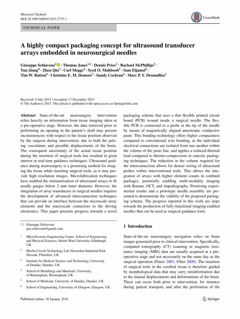
Based on the considerations discussed in the previous paragraphs, the boards have been designed with the bond-ing site joined at 30° to the main interconnection body. Figure 5 shows one of the FPCBs used in this work.
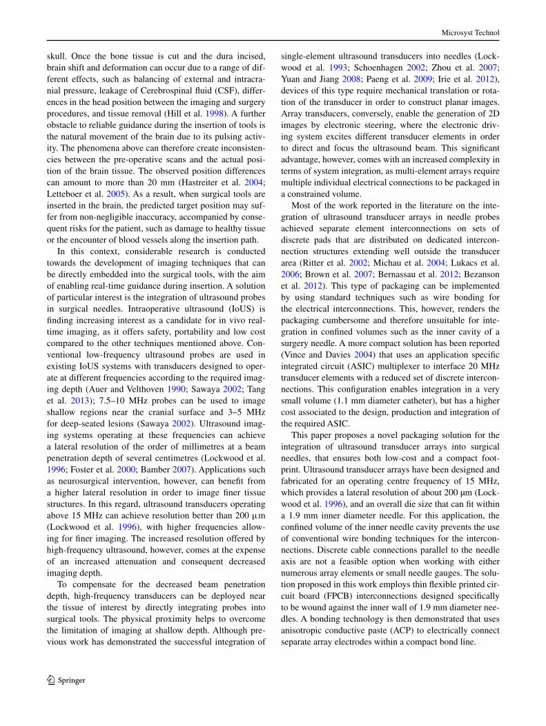
The bonding site at the tip of the flexible interconnec-tion, where the ultrasound transducer is to be placed, is shown in greater detail in Fig. 6, showing the metal tracks
Fig. 4 Optical microscope image of two piezoceramic test dies with patterned electrodes at 100 µm pitch of 1.5 mm by 4 mm size
Microsyst Technol
1 3
patterned at a width of 50 µm, matching the pitch of the ultrasound array electrodes on the die.
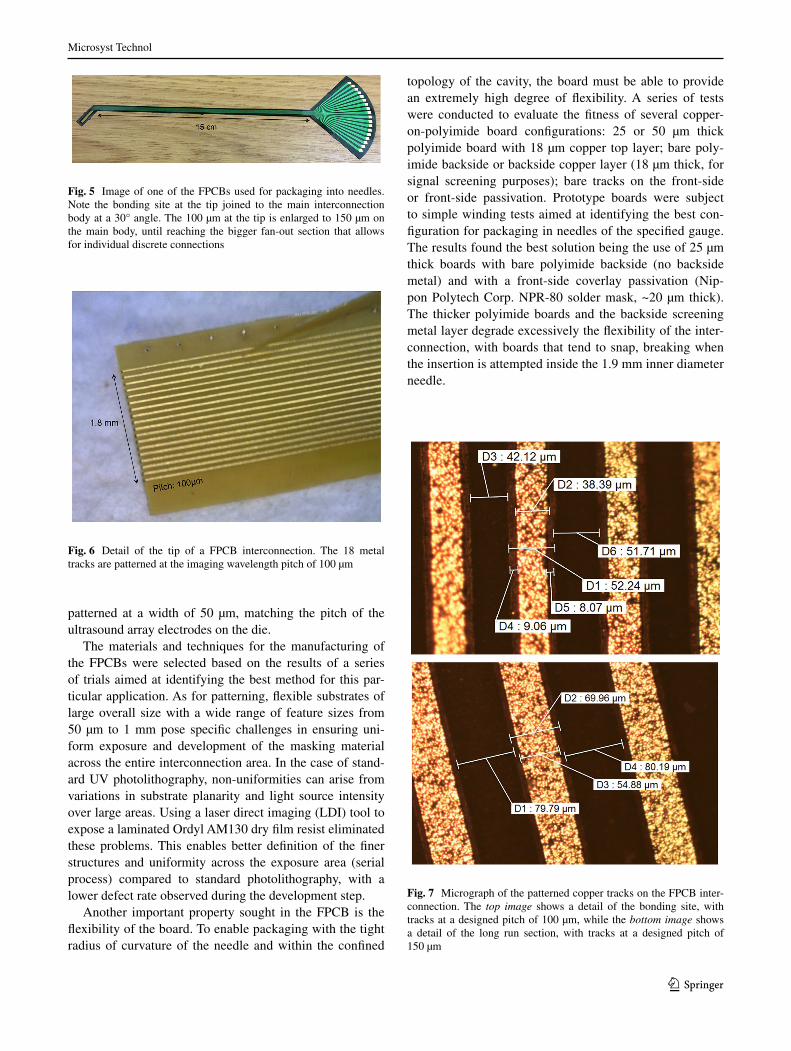
The materials and techniques for the manufacturing of the FPCBs were selected based on the results of a series of trials aimed at identifying the best method for this par-ticular application. As for patterning, flexible substrates of large overall size with a wide range of feature sizes from 50 µm to 1 mm pose specific challenges in ensuring uni-form exposure and development of the masking material across the entire interconnection area. In the case of stand-ard UV photolithography, non-uniformities can arise from variations in substrate planarity and light source intensity over large areas. Using a laser direct imaging (LDI) tool to expose a laminated Ordyl AM130 dry film resist eliminated these problems. This enables better definition of the finer structures and uniformity across the exposure area (serial process) compared to standard photolithography, with a lower defect rate observed during the development step.
Another important property sought in the FPCB is the flexibility of the board. To enable packaging with the tight radius of curvature of the needle and within the confined
topology of the cavity, the board must be able to provide an extremely high degree of flexibility. A series of tests were conducted to evaluate the fitness of several copper-on-polyimide board configurations: 25 or 50 µm thick polyimide board with 18 µm copper top layer; bare poly-imide backside or backside copper layer (18 µm thick, for signal screening purposes); bare tracks on the front-side or front-side passivation. Prototype boards were subject to simple winding tests aimed at identifying the best con-figuration for packaging in needles of the specified gauge. The results found the best solution being the use of 25 µm thick boards with bare polyimide backside (no backside metal) and with a front-side coverlay passivation (Nip-pon Polytech Corp. NPR-80 solder mask, ~20 µm thick). The thicker polyimide boards and the backside screening metal layer degrade excessively the flexibility of the inter-connection, with boards that tend to snap, breaking when the insertion is attempted inside the 1.9 mm inner diameter needle.
Fig. 5 Image of one of the FPCBs used for packaging into needles. Note the bonding site at the tip joined to the main interconnection body at a 30° angle. The 100 µm at the tip is enlarged to 150 µm on the main body, until reaching the bigger fan-out section that allows for individual discrete connections
Fig. 6 Detail of the tip of a FPCB interconnection. The 18 metal tracks are patterned at the imaging wavelength pitch of 100 µm
Fig. 7 Micrograph of the patterned copper tracks on the FPCB inter-connection. The top image shows a detail of the bonding site, with tracks at a designed pitch of 100 µm, while the bottom image shows a detail of the long run section, with tracks at a designed pitch of 150 µm

Microsyst Technol
1 3
Based on the simple board evaluation described above, the flexible interconnections used for prototypes have been fabricated on 25 µm thick polyimide boards coated with a 18 µm thick copper layer and front-side passivation. The copper surface is initially cleaned with a micro-etch pro-cess that removes about 1 µm of the starting thickness. 18 individual electrical connections (16 array elements plus 2 dummy tracks at the two ends) are patterned in the cop-per layer by means of laser direct imaging (LDI) and sub-sequent standard etching in a cupric chloride solution. The copper surface is then finished with a thin electroless plated nickel-gold layer to protect the surface from oxidation. The insulating coverlay is then applied on the whole FPCB sur-face, and vias are finally opened at both ends to expose the gold surface. Figure 7 shows micrographs of the tracks on the bonding site and the long body sections. The size meas-urements shown in Fig. 7 reveal a track underetch that is consistent with the 17 µm copper film thickness at the pat-terning step. This has been further visualised by imaging the cross section of one of the flexible interconnects, shown in Fig. 8.
The FPCB is designed with a shape and length that ena-ble insertion in an 80 mm long, 1.9 mm inner diameter nee-dle by winding the board into the cavity at a specific angle, using a smaller diameter rod as a guide. The layout of the interconnection ensures that when the FPCB is fed through the needle by wrapping, the bonding site reaches the tip parallel to the needle axis. Figure 9 shows an FPCB pack-aged inside a needle, with the tip of the interconnection out of the tip of the needle to allow for bonding.
4 Die bonding
The piezo-transducing die, which serves as the ultrasound probe, must be bonded onto the flexible interconnection structures. To this end, the FPCB is fed through the housing needle until the fine pitch strip reaches the tip, as shown in Fig. 9. Figure 10 shows a detail of the bonding site on the
FPCB at the tip of the packaging needle as seen from the bonding tool.
The challenge of this particular application lies in the limitations on the thermal budget and pressure that the pie-zoceramic can withstand. Excessive process temperatures can cause the material to suffer from depoling and there-fore losing the piezoelectric properties. Piezoceramics are also very brittle and cannot withstand the pressures that are typical of standard thermo-compression or eutectic tech-niques. An alternative bonding process is therefore required that ensures compactness to fit the small volume of the nee-dle housing, while preserving the transducer material.
Fig. 8 Cross section micrograph of the bonding site of an FPCB interconnection
Fig. 9 Detail of the tip of a FPCB interconnection. The metal tracks are patterned at the imaging wavelength pitch of 100 µm
Fig. 10 Detail of the bonding site of the FPCB fed through the nee-dle bore. The outer diameter of the needle is 2 mm
Microsyst Technol
1 3
A technique that has recently gained interest in the pack-aging community is bonding with anisotropic conductive adhesives. Such technologies offer a highly compact foot-print, as they enable the required electrical interconnections to be created within the volume of adhesive used for die placement.
The two types of anisotropic adhesives that have been developed are pastes and films. Both media contain embed-ded conductive particles that are used to locally form elec-trical bridges. Specifically, films create electrical interfaces by exploiting the topography of pads. A portion of adhe-sive is placed between the die and the substrate and, when sufficient pressure is applied, the pads on the two facing surfaces squeeze the film until the embedded beads form a pad-to-pad conductive path. The bonding force required to create such connections, however, is typically of the order of 0.2–0.8 kg per pad for chip on flex applications (Dexeri-als corporation, personal communication). This exceeds the brittle strength of the piezoceramic used, which can easily shatter even when subject to the low force required for pick and place operations. Moreover, the typical curing tempera-tures for anisotropic conductive films (>150 °C) exceed the working temperatures of the piezoelectric materials used.
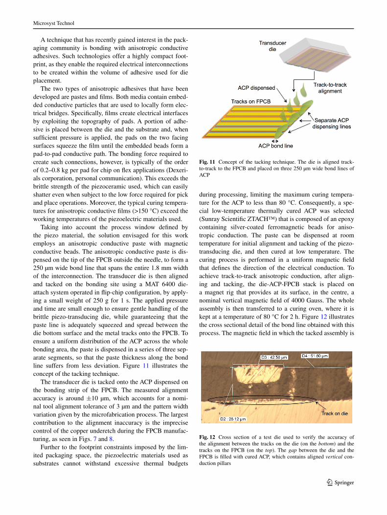
Taking into account the process window defined by the piezo material, the solution envisaged for this work employs an anisotropic conductive paste with magnetic conductive beads. The anisotropic conductive paste is dis-pensed on the tip of the FPCB outside the needle, to form a 250 µm wide bond line that spans the entire 1.8 mm width of the interconnection. The transducer die is then aligned and tacked on the bonding site using a MAT 6400 die-attach system operated in flip-chip configuration, by apply-ing a small weight of 250 g for 1 s. The applied pressure and time are small enough to ensure gentle handling of the brittle piezo-transducing die, while guaranteeing that the paste line is adequately squeezed and spread between the die bottom surface and the metal tracks onto the FPCB. To ensure a uniform distribution of the ACP across the whole bonding area, the paste is dispensed in a series of three sep-arate segments, so that the paste thickness along the bond line suffers from less deviation. Figure 11 illustrates the concept of the tacking technique.
The transducer die is tacked onto the ACP dispensed on the bonding strip of the FPCB. The measured alignment accuracy is around ±10 µm, which accounts for a nomi-nal tool alignment tolerance of 3 µm and the pattern width variation given by the microfabrication process. The largest contribution to the alignment inaccuracy is the imprecise control of the copper underetch during the FPCB manufac-turing, as seen in Figs. 7 and 8.
Further to the footprint constraints imposed by the lim-ited packaging space, the piezoelectric materials used as substrates cannot withstand excessive thermal budgets
during processing, limiting the maximum curing tempera-ture for the ACP to less than 80 °C. Consequently, a spe-cial low-temperature thermally cured ACP was selected (Sunray Scientific ZTACH™) that is composed of an epoxy containing silver-coated ferromagnetic beads for aniso-tropic conduction. The paste can be dispensed at room temperature for initial alignment and tacking of the piezo-transducing die, and then cured at low temperature. The curing process is performed in a uniform magnetic field that defines the direction of the electrical conduction. To achieve track-to-track anisotropic conduction, after align-ing and tacking, the die-ACP-FPCB stack is placed on a magnet rig that provides at its surface, in the centre, a nominal vertical magnetic field of 4000 Gauss. The whole assembly is then transferred to a curing oven, where it is kept at a temperature of 80 °C for 2 h. Figure 12 illustrates the cross sectional detail of the bond line obtained with this process. The magnetic field in which the tacked assembly is
Fig. 11 Concept of the tacking technique. The die is aligned track-to-track to the FPCB and placed on three 250 µm wide bond lines of ACP
Fig. 12 Cross section of a test die used to verify the accuracy of the alignment between the tracks on the die (on the bottom) and the tracks on the FPCB (on the top). The gap between the die and the FPCB is filled with cured ACP, which contains aligned vertical con-duction pillars
Microsyst Technol
1 3
immersed during the curing process arranges the conduc-tive particles in vertical pillars that connect the tracks on the die to the corresponding tracks on the FPCB. The mag-netically-aligned vertically-assembled pillars of conductive beads are visible in Fig. 12.
The technique used for this work therefore reduces the volume required by the electrical interconnection between the die and the board, compared to standard wire-bonding solutions. The use of an anisotropic conductive paste with magnetically aligned conductive beads that can be cured at low temperature reduces the pressure and temperature required for packaging. This technique is therefore per-fectly suited for the interconnection of brittle piezoceramic dies used to produce ultrasound array transducers.
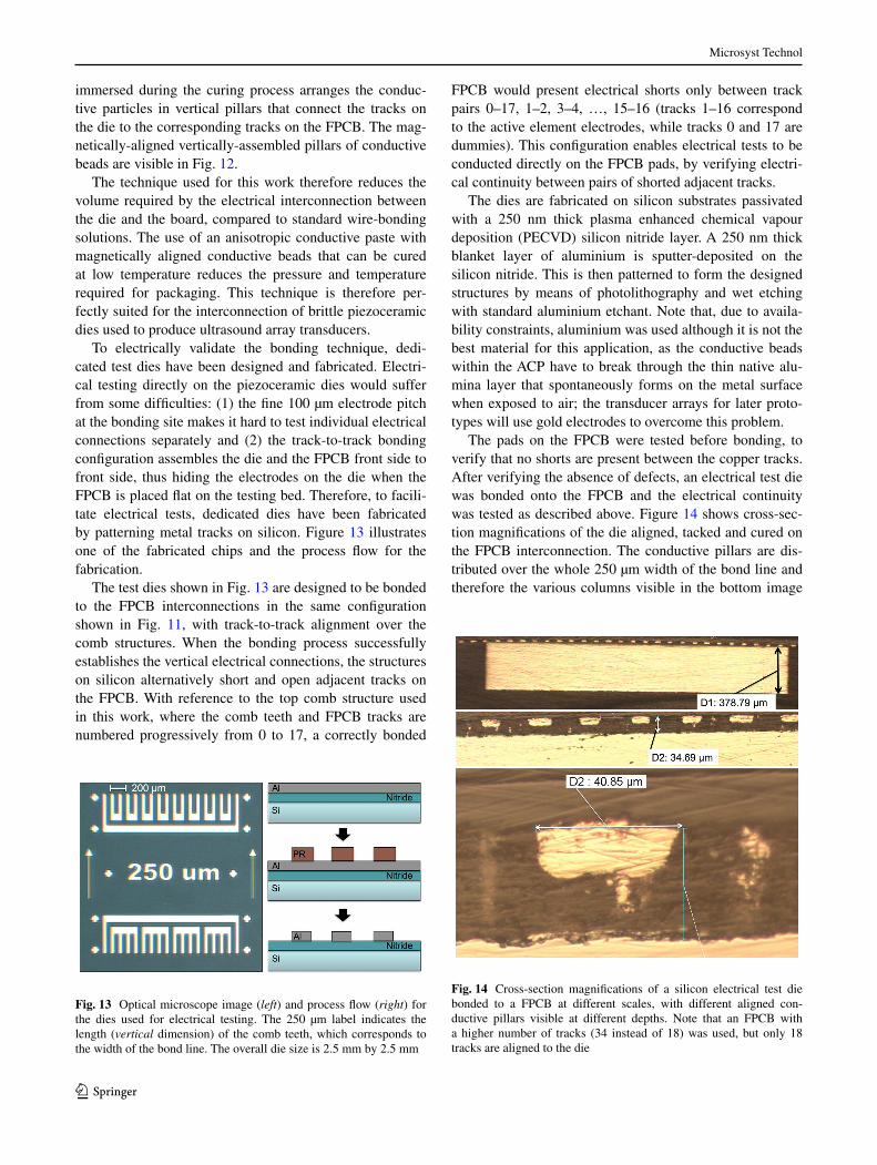
To electrically validate the bonding technique, dedi-cated test dies have been designed and fabricated. Electri-cal testing directly on the piezoceramic dies would suffer from some difficulties: (1) the fine 100 µm electrode pitch at the bonding site makes it hard to test individual electrical connections separately and (2) the track-to-track bonding configuration assembles the die and the FPCB front side to front side, thus hiding the electrodes on the die when the FPCB is placed flat on the testing bed. Therefore, to facili-tate electrical tests, dedicated dies have been fabricated by patterning metal tracks on silicon. Figure 13 illustrates one of the fabricated chips and the process flow for the fabrication.
The test dies shown in Fig. 13 are designed to be bonded to the FPCB interconnections in the same configuration shown in Fig. 11, with track-to-track alignment over the comb structures. When the bonding process successfully establishes the vertical electrical connections, the structures on silicon alternatively short and open adjacent tracks on the FPCB. With reference to the top comb structure used in this work, where the comb teeth and FPCB tracks are numbered progressively from 0 to 17, a correctly bonded
FPCB would present electrical shorts only between track pairs 0–17, 1–2, 3–4, …, 15–16 (tracks 1–16 correspond to the active element electrodes, while tracks 0 and 17 are dummies). This configuration enables electrical tests to be conducted directly on the FPCB pads, by verifying electri-cal continuity between pairs of shorted adjacent tracks.
The dies are fabricated on silicon substrates passivated with a 250 nm thick plasma enhanced chemical vapour deposition (PECVD) silicon nitride layer. A 250 nm thick blanket layer of aluminium is sputter-deposited on the silicon nitride. This is then patterned to form the designed structures by means of photolithography and wet etching with standard aluminium etchant. Note that, due to availa-bility constraints, aluminium was used although it is not the best material for this application, as the conductive beads within the ACP have to break through the thin native alu-mina layer that spontaneously forms on the metal surface when exposed to air; the transducer arrays for later proto-types will use gold electrodes to overcome this problem.
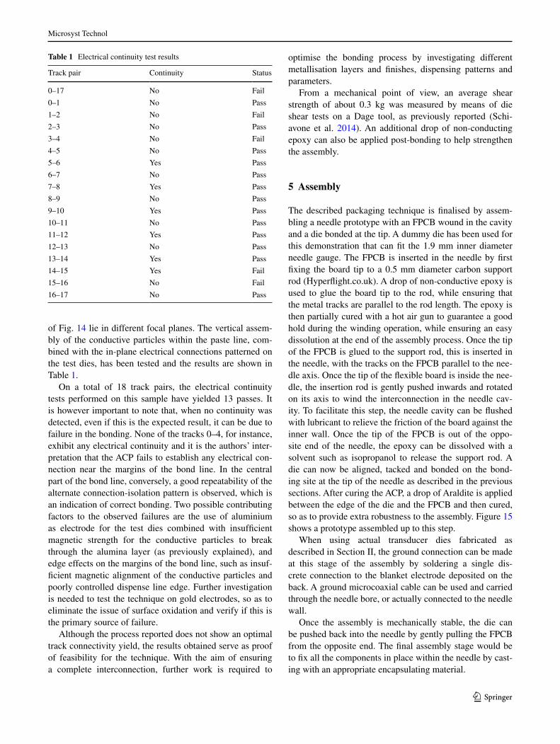
The pads on the FPCB were tested before bonding, to verify that no shorts are present between the copper tracks. After verifying the absence of defects, an electrical test die was bonded onto the FPCB and the electrical continuity was tested as described above. Figure 14 shows cross-sec-tion magnifications of the die aligned, tacked and cured on the FPCB interconnection. The conductive pillars are dis-tributed over the whole 250 µm width of the bond line and therefore the various columns visible in the bottom image
Fig. 13 Optical microscope image (left) and process flow (right) for the dies used for electrical testing. The 250 µm label indicates the length (vertical dimension) of the comb teeth, which corresponds to the width of the bond line. The overall die size is 2.5 mm by 2.5 mm
Fig. 14 Cross-section magnifications of a silicon electrical test die bonded to a FPCB at different scales, with different aligned con-ductive pillars visible at different depths. Note that an FPCB with a higher number of tracks (34 instead of 18) was used, but only 18 tracks are aligned to the die
Microsyst Technol
1 3
of Fig. 14 lie in different focal planes. The vertical assem-bly of the conductive particles within the paste line, com-bined with the in-plane electrical connections patterned on the test dies, has been tested and the results are shown in Table 1.
On a total of 18 track pairs, the electrical continuity tests performed on this sample have yielded 13 passes. It is however important to note that, when no continuity was detected, even if this is the expected result, it can be due to failure in the bonding. None of the tracks 0–4, for instance, exhibit any electrical continuity and it is the authors’ inter-pretation that the ACP fails to establish any electrical con-nection near the margins of the bond line. In the central part of the bond line, conversely, a good repeatability of the alternate connection-isolation pattern is observed, which is an indication of correct bonding. Two possible contributing factors to the observed failures are the use of aluminium as electrode for the test dies combined with insufficient magnetic strength for the conductive particles to break through the alumina layer (as previously explained), and edge effects on the margins of the bond line, such as insuf-ficient magnetic alignment of the conductive particles and poorly controlled dispense line edge. Further investigation is needed to test the technique on gold electrodes, so as to eliminate the issue of surface oxidation and verify if this is the primary source of failure.
Although the process reported does not show an optimal track connectivity yield, the results obtained serve as proof of feasibility for the technique. With the aim of ensuring a complete interconnection, further work is required to
optimise the bonding process by investigating different metallisation layers and finishes, dispensing patterns and parameters.
From a mechanical point of view, an average shear strength of about 0.3 kg was measured by means of die shear tests on a Dage tool, as previously reported (Schi-avone et al. 2014). An additional drop of non-conducting epoxy can also be applied post-bonding to help strengthen the assembly.
5 Assembly
The described packaging technique is finalised by assem-bling a needle prototype with an FPCB wound in the cavity and a die bonded at the tip. A dummy die has been used for this demonstration that can fit the 1.9 mm inner diameter needle gauge. The FPCB is inserted in the needle by first fixing the board tip to a 0.5 mm diameter carbon support rod (Hyperflight.co.uk). A drop of non-conductive epoxy is used to glue the board tip to the rod, while ensuring that the metal tracks are parallel to the rod length. The epoxy is then partially cured with a hot air gun to guarantee a good hold during the winding operation, while ensuring an easy dissolution at the end of the assembly process. Once the tip of the FPCB is glued to the support rod, this is inserted in the needle, with the tracks on the FPCB parallel to the nee-dle axis. Once the tip of the flexible board is inside the nee-dle, the insertion rod is gently pushed inwards and rotated on its axis to wind the interconnection in the needle cav-ity. To facilitate this step, the needle cavity can be flushed with lubricant to relieve the friction of the board against the inner wall. Once the tip of the FPCB is out of the oppo-site end of the needle, the epoxy can be dissolved with a solvent such as isopropanol to release the support rod. A die can now be aligned, tacked and bonded on the bond-ing site at the tip of the needle as described in the previous sections. After curing the ACP, a drop of Araldite is applied between the edge of the die and the FPCB and then cured, so as to provide extra robustness to the assembly. Figure 15 shows a prototype assembled up to this step.
When using actual transducer dies fabricated as described in Section II, the ground connection can be made at this stage of the assembly by soldering a single dis-crete connection to the blanket electrode deposited on the back. A ground microcoaxial cable can be used and carried through the needle bore, or actually connected to the needle wall.
Once the assembly is mechanically stable, the die can be pushed back into the needle by gently pulling the FPCB from the opposite end. The final assembly stage would be to fix all the components in place within the needle by cast-ing with an appropriate encapsulating material.
Table 1 Electrical continuity test results
Track pair Continuity Status
0–17 No Fail
0–1 No Pass
1–2 No Fail
2–3 No Pass
3–4 No Fail
4–5 No Pass
5–6 Yes Pass
6–7 No Pass
7–8 Yes Pass
8–9 No Pass
9–10 Yes Pass
10–11 No Pass
11–12 Yes Pass
12–13 No Pass
13–14 Yes Pass
14–15 Yes Fail
15–16 No Fail
16–17 No Pass

Microsyst Technol
1 3
6 Conclusions
This article addressed the challenge of packaging ultra-sound transducer dies at the tip of small gauge surgical tools such as needles. A compact packaging concept was presented that reduces the footprint of such devices so as to fit 1.9 mm inner diameter needles. Flexible printed cir-cuit boards have been designed and manufactured to carry the interconnections through the length of the needle. The boards are wound against the inner wall of the needle and provide at the tip a flat strip that is used to bond transducer dies. To the authors’ knowledge, this work reports for the first time the use of a flexible substrate as a multi-track interconnect medium that can be rolled around the inner walls of a surgical needle to carry a larger number of inter-connections than normally possible with conventional tech-niques. The results presented herein demonstrate the fea-sibility of manufacturing dense multi-track flexible boards specifically designed for the integration of functional probes into small gauge surgery needles.
A bonding technique was also presented that pro-vides electrical connections in a very compact space, by means of a magnetically aligned anisotropic conductive paste. Progress was presented towards achieving satis-factory reliability of the technology in terms of mechani-cal robustness and electrical continuity. The developed technique was applied to a test die specifically designed and fabricated to probe the selective electrical continu-ity through the bond line. The experiment reported shows promising results, with 13 out of the 18 electrical inter-faces working as intended. A discussion of the achieved performance was presented, along with directions for future investigation and improvement. Further work is required to optimise the process yield and ensure that all the electrical interfaces are correctly formed. Specifically, a gold metallisation or finishing is desirable to avoid the formation of an oxide barrier at the surface that can impede conductive beads in the paste to make an electri-cal contact. Moreover, the paste dispensing step prior to the die attach may also be optimised by modifying the
paste line patterns on the board and/or the time-pressure dispensing parameters. The paste composition may also be modified by changing the mixing ratio of the two ACP parts. A balance must be found to obtain a sufficient con-ductive bead density, adequate viscosity to facilitate the dispensing without resulting in excessive spread on the board, and thickness uniformity throughout the bond line. Finally, an optimised magnetic rig may also be designed so as to provide a more uniform magnetic field direc-tionality. This will ensure that during the curing process the conductive beads in the paste are aligned into pillars along the vertical direction throughout the bond line, with no deviation at the margins.
A prototype was finally built using one of the produced FPCBs and the proposed bonding technique. The success-ful construction of this dummy device proves the feasibility of the proposed packaging configuration and represents an important stepping stone towards the production of func-tional imaging-enabled surgical needles for use in neuro-surgery intervention. Future devices with increased func-tionality will be tested for fitness as imaging tools in the human body to aid surgical intervention.
Acknowledgments The authors would like to acknowledge the financial support of the Engineering and Physical Science Research Council (EPSRC) through the funding of the research grant entitled “Ultrasound in a Needle, USINN” and referenced EP/K020250/1. The authors would also like to thank Merlin Circuit Technology Ltd, part of the Falcon Group, for the fabrication of the flexible printed circuit boards used in this research.
Open Access This article is distributed under the terms of the Crea-tive Commons Attribution 4.0 International License (http://creativecom-mons.org/licenses/by/4.0/), which permits unrestricted use, distribution, and reproduction in any medium, provided you give appropriate credit to the original author(s) and the source, provide a link to the Creative Commons license, and indicate if changes were made.
References
Auer LM, Velthoven V (1990) Intraoperative ultrasound imaging in neurosurgery. Springer, Berlin
Bamber JC (2007) Acoustical characteristics of biological media. Encyclopedia of acoustics. Wiley, Hoboken, pp 1703–1726
Bernassau AL, Garcia-Gancedo L, Hutson D, Demore CEM, McAneny JJ, Button TW, Cochran S (2012) Microfabrica-tion of electrode patterns for high-frequency ultrasound trans-ducer arrays. IEEE Trans Ultrason Ferroelectr Freq Control 59(8):1820–1829
Bezanson A, Garland P, Adamson R, Brown JA (2012) Fabrication of a miniaturized 64-element high-frequency phased array. In: 2012 IEEE international ultrasonics symposium, pp 2114–2117
Brown JA, Foster FS, Needles A, Cherin E, Lockwood GR (2007) Fabrication and performance of a 40-MHz linear array based on a 1–3 composite with geometric elevation focusing. IEEE Trans Ultrason Ferroelectr Freq Control 54(9):1888–1894
El Gammal S, El Gammal C, Kaspar K, Pieck C, Altmeyer P, Vogt M, Ermert H (1999) Sonography of the skin at 100 MHz enables
Fig. 15 Assembled prototype of a 80 mm long, 1.9 mm inner diam-eter needle with a dummy die bonded to an FPCB interconnection wound in the inner cavity

Microsyst Technol
1 3
in vivo palmar skin and psoriatic plaques. J Invest Dermatol 113(5):821–829
Filler AG (2009) The history, development and impact of computed imaging in neurological diagnosis and neurosurgery: CT, MRI, and DTI. Nat Precedings 7:1–69
Foster FS, Pavlin CJ, Harasiewicz KA, Christopher DA, Turnbull DH (2000) Advances in ultrasound biomicroscopy. Ultrasound Med Biol 26(1):1–27
Hastreiter P, Rezk-Salama C, Soza G, Bauer M, Greiner G, Fahlbusch R, Ganslandt O, Nimsky C (2004) Strategies for brain shift eval-uation. Med Image Anal 8:447–464
Hill DL, Maurer CR Jr, Maciunas RJ, Barwise JA, Fitzpatrick MJ, Wang MY (1998) Measurement of intraoperative brain surface deformation under a craniotomy. Neurosurgery 43:514–526
Irie T, Hasegawa T, Sato M, Tagawa N, Tanabe M, Yoshizawa M, Iijima T, Moriya T, Itoh K (2012) Transmission of 100-MHz-range ultrasound through a fused quartz fiber. In: 2012 IEEE international ultrasonics symposium, pp 358–361
Letteboer MMJ, Willems PW, Viergever MA, Niessen WJ (2005) Brain shift estimation in image-guided neurosurgery using 3-D ultrasound. IEEE Trans Biomed Eng 52:268–276
Lockwood GR, Ryan LK, Foster FS (1993) A 45 to 55 MHz needle-based ultrasound system for invasive imaging. Ultrason Imaging 15(1):1–13
Lockwood GR, Turnball DH, Christopher DA, Foster FS (1996) Beyond 30 MHz applications of high-frequency ultrasound imaging. IEEE Eng Med Biol Mag 15(6):60–71
Lukacs M, Yin J, Pang G, Garcia R, Cherin E, Williams R, Mehi J, Foster F (2006) Performance and characterization of new micromachined high-frequency linear arrays. IEEE Trans Ultra-son Ferroelectr Freq Control 53(10):1719–1729
Michau S, Mauchamp P, Dufait R (2004) Piezocomposite 30 MHz linear array for medical imaging: design challenges and perfor-mances evaluation of a 128 elements array. In: Proceedings 2004 IEEE ultrasonics symposium, vol 2, pp 898–901
Paeng DG, Chang JH, Chen R, Humayun MS, Shung KK (2009) Fea-sibility of rotational scan ultrasound imaging by an angled high frequency transducer for the posterior segment of the eye. IEEE Trans Ultrason Ferroelectr Freq Control 56(3):676–680
Peters TM (2001) Image-guided surgery: from X-rays to virtual real-ity. Comput Methods Biomech Biomed Eng 4:27–57
Ritter TA, Shrout TR, Tutwiler R, Shung KK (2002) A 30 MHz piezo-composite ultrasound array for medical imaging applications. IEEE Trans Ultrason Ferroelectr Freq Control 49(2):217–230
Sawaya R (2002) Radical resection of glioblastoma: techniques and benefits. Contemp Neurosurg 24:1–5
Schiavone G, Jones T, Price D, McPhillips R, Qiu Z, Demore CEM, Jiang Y, Meggs C, Mahboob SO, Eljamel S, Button TW, Cochran S, Desmulliez MPY (2014) Advanced electrical array intercon-nections for ultrasound probes integrated in surgical needles. In: 2014 IEEE 16th electronics packaging technology conference (EPTC), pp 88–93
Schoenhagen P (2002) Understanding coronary artery disease: tomographic imaging with intravascular ultrasound. Heart 88(1):91–96
Tang H, Sun H, Xie L, Tang Q, Gong Y, Mao Y, Xie Q, Zheng M, Wang D, Zhu H (2013) Intraoperative ultrasound assistance in resection of intracranial meningiomas. Chin J Cancer Res 25:339
Vince DG, Davies SC (2004) Peripheral application of intravascular ultrasound virtual histology. Semin Vasc Surg 17(2):119–125
Yuan J, Jiang XN (2008) 60 MHz PMN-PT based 1–3 composite transducer for IVUS imaging. In: 2008 IEEE ultrasonics sympo-sium, pp 682–685
Zhou Q, Xu X, Gottlieb E, Sun L, Cannata J, Ameri H, Humayun M, Han P, Shung K (2007) PMN-PT single crystal, high-fre-quency ultrasonic needle transducers for pulsed-wave Dop-pler application. IEEE Trans Ultrason Ferroelectr Freq Control 54(3):668–675