a highly integrated analog front-end for 3g - solid-state...
TRANSCRIPT

774 IEEE JOURNAL OF SOLID-STATE CIRCUITS, VOL. 38, NO. 5, MAY 2003
A Highly Integrated Analog Front-End for 3GWaleed Khalil, Tsung-Yuan Chang, Xuewen Jiang, Syed R. Naqvi, Babak Nikjou, and James Tseng
Abstract—This paper describes a reconfigurable analogfront-end (AFE) and audio Codec IC supporting the widebandcode division multiple access (WCDMA) standard. The chip isfabricated on Intel’s 0.18- m (SOC) flash+ logic+ analog (FLA)process technology using a 0.35-m feature size analog transistor.The transmit path contains a 10-bit segmented rail-to-rail dig-ital-to-analog converter, automatically tunable active RC filter,and programmable gain amplifier (PGA) with self-tuning gainand offset correction circuit. The receive path incorporates aPGA, active RC filter, and an 8-bit analog-to-digital converterwith built-in offset correction. The AFE operates at 2.7 V with acurrent consumption of 55 mA and total active area of 15 mm2.
Index Terms—Active RC filter, analog baseband, analogfront-end (AFE), programmable gain amplifier (PGA), wirelesstransmitters and receivers.
I. INTRODUCTION
W IDEBAND code division multiple access (WCDMA)is predicted to become the most dominant stan-
dard when the cellphone industry transitions from voice tohigh-datarate-based applications such as video transmissionand interactive video games. In comparison with a GSMsystem that uses 200-kHz channel spacing, WCDMA uses5-MHz channel spacing and is, therefore, able to achieve amaximum data rate of 2 Mb/s. In order to adjust to this orderof magnitude increase in bandwidth from GSM to WCDMA, anew architecture is developed for the analog front-end (AFE)[1].
Combining analog and digital baseband along with Flash andSRAM memory on a single die provides the ultimate integrationfor a cellular system-on-chip (SOC). Although this integrationachieves the best performance and lowest power/area, it resultsin a noisy environment that is hostile to analog circuits. In ad-dition, previous attempts to achieve this level of integration re-sulted in sacrificing the performance of the analog and/or dig-ital transistor. This paper describes a reconfigurable AFE fabri-cated on Intel’s advanced flashlogic analog (FLA) processtechnology. This AFE integration with digital and flash achievesdie-area and power savings unattainable by using multicompo-nent chipsets.
This paper covers the major blocks in the WCDMA AFEtransceiver, with major focus on the transmit side. The organ-ization of this paper is as follows. Section II presents an overallreview of the chip architecture. Section III details the transmitterpart of the AFE, including the digital-to-analog converter (D/A),filter, and programmable gain amplifier (PGA). Section IV dis-cusses the receiver part of the AFE. The layout and experimental
Manuscript received August 2, 2002; revised December 18, 2002.The authors are with Intel Corporation, Chandler, AZ 85226 USA (e-mail:
[email protected]).Digital Object Identifier 10.1109/JSSC.2003.810059
Fig. 1. Typical wireless system.
results are presented in Section V. Finally, in Section VI, thepaper concludes with a summary.
II. AFE ARCHITECTURE
Fig. 1 illustrates a typical wireless system, where three dis-tinct sections are shown. The RF front-end section is responsiblefor amplification as well as downconverting/upconverting of theRF signal to/from low-frequency baseband signal. The base-band AFE processes the signal in the low-frequency domain. Inthe receiver part of the AFE (also known as the demodulator),the small signal is further gained and filtered, then digitizedusing an analog-to-digital coonverter (A/D). The AFE trans-mitter (known as the modulator) is responsible for convertingdigitally modulated symbols into an analog signal using a D/A,followed by filtering and gain stages. The auxiliary section ismainly responsible for controlling the RF system as well as gen-eral phone functions. Last is the digital baseband module, whichis used for the main digital modulation and demodulation/detec-tion functions. A detailed description of the specifications forthe WCDMA system is available on the 3GPP website.1
A block diagram detailing the architecture of the AFE isshown in Fig. 2, where the main channels are the transmitchannel, receive channel, and auxiliary channel. In the transmitchannel, 10-bit digitally modulated data is received from thedigital section of baseband modem by the– D/A. Thearchitecture of the 10-bit D/A is based on a fully differentialsegmented voltage mode R-2R, reported for the first time atthe high sampling rate of 15.36 MHz. The R-2R architectureutilizes a ladder network of R-2R resistors to obtain binaryweighted voltages. Following the D/A is the transmitter (TX)filter, which limits the bandwidth of the signal to the channelbandwidth and reduces any spurious emission caused by theD/A glitch energy. The TX filter is a fifth-order ButterworthactiveRC filter with power-on self-calibration. The filter relieson a 4-bit capacitor trimming approach to achieve 7%bandwidth accuracy, while achieving a passband gain flatness
1[Online.] Available: http://www.3gpp.org/specs/specs.htm
0018-9200/03$17.00 © 2003 IEEE

KHALIL et al.: HIGHLY INTEGRATED ANALOG FRONT-END FOR 3G 775
Fig. 2. AFE block diagram.
of dB and total harmonic distortion (THD) dB.Following the filter, a five-level PGA is used to adjust theoutput signal level and automatically calibrate the channeloffset error upon the transmitter power-on or system request.
In the receive path, an input buffer is used in the first stageto perform two important functions: as a high-pass filter for dcoffset blocking, and to improve the third-order input interceptpoint (IIP3) of the receiver through reducing the inter-modu-lation distortion (IMD) level. Following the buffer is a combi-nation of a fourth-order Butterworth activeRC filter and PGA.Finally, an 8-bit 15.36-MS/s A/D is used along with built-inmultibit D/A for channel offset correction. The output data ofthe A/D is consequently latched and sent to the digital basebandmodem
The auxiliary path includes a 10-bit cyclic A/D used for con-trol purposes (e.g., battery testing) along with six R-string D/Asfor RF control functions. A 4-bit serial bus is used as the dig-ital interface for the chip to control both the AFE and the audioCodec.
III. T RANSMITTER DESIGN
The requirements for a transmitter are dictated by the de-sired bit error rate (BER) and the adjacent channel power ratio(ACPR) after digital filtering in the baseband. The transmitterhas two symmetrical channels, namely, in-phase (channel)and quadrature ( channel). The transmit signal generated bythe baseband processor is a hybrid phase shift keying (HPSK)modulated digital signal with a bandwidth of 1.92 MHz. This1.92-MHz digital signal is 4 oversampled by the D/A at a sam-pling frequency of 15.36 MHz. The transmit frequency maskprimarily dictates the filter transition band and stop-band profilein order to minimize spurious emissions and adjacent channelleakage. Additionally, the image attenuation requirement at thesampling frequency is another key factor for the filter rolloff.With a five-pole Butterworth filter, a 100-dB/decade rolloff isachieved, ensuring a 48-dB attenuation of the image that ap-pears between 13.44–17.28 MHz, as shown in Fig. 3.
Fig. 3. Frequency spectrum of the transmit signal with the filter rolloffsuperimposed.
Fig. 4. General architecture and circuit of theI-mode D/A.
A. TX-IQ D/A
The – D/A is the major building block that converts thebinary-weighted digital input signal to a proportional analogvoltage level. The goal of the D/A reported here is to obtainintrinsic 9-bit accuracy for sampling speeds up to 15.36 MS/s.There are several factors that are usually considered during theD/A design process. The D/A resolution, clock rate, and spectralpurity, as well as area and power efficiency, are key parametersthat ultimately affect the overall system performance. First, areview of the -mode D/A (the most common D/A architecture)will be presented. Then, a detailed discussion of the selectedR-2R D/A will follow.
Current-steering (-mode) D/As are typically the architectureof choice for medium- to high-speed applications [2].-modeD/As are based on an array of matched current cells organizedin unary or binary weighted elements that are steered to the D/Aoutput depending on the digital input code, as shown in Fig. 4.Architecture variants include two-stage, interpolated, and seg-mented current-steering architectures. The segmented architec-ture is the most frequently used to combine high conversionrate and high resolution. In this architecture, the least signifi-cant bits (LSBs) steer binary weighted current sources, whilethe most significant bits (MSBs) are thermometer encoded andsteer a unary current source array. Special biasing techniquesand switching sequence optimization are often used in these ar-chitectures to spatially average away the systematic and randomthreshold voltage mismatch of the current cells [3]. Since the-mode D/A uses active devices only, it is compatible with dig-
ital CMOS processes and is inherently a high-speed architec-ture. However, this architecture has some limitations in termsof power and area efficiency for the targeted speed and requiredresolution. Since reducing the cell current leads to lower tran-sistor overdrive voltage, the effect of threshold voltagemis-match is magnified. This limits the raw resolution (without trim-ming/calibration) of the -mode D/A to around eight bits. Inorder to get around this problem, the transistor size in the current

776 IEEE JOURNAL OF SOLID-STATE CIRCUITS, VOL. 38, NO. 5, MAY 2003
Fig. 5. Block diagram of the 10-bit segmented R-2R D/A.
cell (area and channel length) is increased, hence, increasingthe transistor overdrive voltage while decreasing the effect of
mismatch. Although this helps in reducing the effect ofmismatch, it translates to excessive growth in area and capaci-tance, which limits the switching speed. Another solution to thisproblem is to increase the cell current, but this leads to higherpower dissipation. Therefore, sacrificing either area or power isseen to be the fundamental limitation of the-mode D/A.
A very popular architecture for the D/A uses R-2R ladders[4]. These ladders are used to realize binary weighted currentsor voltages with a small number of components using a resis-tance ratio of only 2 : 1, independent of the number of bits ofresolution. The R-2R approach is compatible with both bipolarand CMOS technologies and is found to be highly efficient inresistor usage for D/As ranging from 6 to 16 bits. However,there are some disadvantages of the R-2R ladder architecture.In general, it requires good resistor matching to guarantee lin-earity and monotonicity. The switching transients at major codetransitions also produce relatively large glitches. The proposedimplementation uses segmentation and random walk techniquesto realize a low-voltage, low-power, and area-efficient topologyfor an intrinsic 9-bit accuracy, without the need for trimming,calibration, tuning, or dynamic averaging.
In an R-2R ladder, it is necessary to have tight matching be-tween each bit and the sum of all lesser bits in order to ensuremonotonic operation. The segmented architecture allows this re-quirement to be relaxed and permits the construction of high-resolution converters. The block diagram of a 4/6 segmented10-bit voltage division R-2R D/A is shown in Fig. 5, in whichthe coarse D/A consists of 2 identical resistors (1–15 2Rs),which are selected by a thermometer code. It is worth notingthat for an R-2R ladder, the mismatch errors at the left end ofthe ladder are less significant than those at the right end (thesegmented section). Consequently, large errors in the LSB re-sistors contribute proportionally less to the overall error thanmuch smaller errors in the segmented resistors. Qualitatively,this is because the full-scale error due to a fractional error inan LSB is smaller than the same fractional error in an MSB.This observation indicates that more effort should be devoted tomatching the segment resistors in the MSBs of the ladder thanin the LSBs, since the former are more likely to determine thefinal accuracy than the latter.
In order to further reduce the sensitivity to resistor matching,a novel random-walk layout technique was utilized. This tech-
Fig. 6. Random walk technique for the segmented R-2R ladder.
(a) (b)
Fig. 7. A plot of resistor length versus resistor sequence (1–15 2Rs): (a)�1%linearL mismatch. (b)�2% randomL mismatch.
nique has been used very recently in a high-resolution current-steering D/A to realize 14-bit intrinsic accuracy [5]. The basicidea behind random walk is to average between positive differ-ential nonlinearity (DNL) and negative DNL errors through hi-erarchical randomization. This technique (Fig. 6) improves thenonlinearity across process variations, since every 2R resistorfor the same unary code is randomly placed to prevent first- andsecond-order systematic error residues from accumulating in theD/A output. In addition, mixing the upper and lower resistor lad-ders of the differential D/A helps in minimizing the differentialoffset error.
A simple Matlab program was used to demonstrate thestrength of the random-walk layout technique. The simulationwas done to compare between the D/A integral nonlinearity(INL) for 1 linear dimension mismatch and those for2random dimension mismatch in the segmented MSB portion.Fig. 7 shows a plot of the length of the resistors () versus theresistor sequence (1–15 2R segmented resistors) for the linearand random mismatch cases. The resistor width was kept thesame for both cases. The random dimension mismatch datawas generated using a normal distribution.
The INL analysis for 1 linear mismatch and 2 randommismatch is shown in Fig. 8. For the1 linear mismatch case,in which there is no spatial averaging effect, INL errors are ac-cumulated as the digital input code increases. The maximumINL error is 2.5 LSB, which results in 8.5-bit accuracy for the10-bit D/A. However, for the case of2 random mismatch,although the absolute mismatch magnitude is doubled comparedto the linear case, the combined effect is a very desirable1.2LSB INL error, which results in a 9.8-bit accuracy for the 10-bitD/A. This is because the residual error above average and theresidual error below average randomly compensate each otheras the digital input code increases.
A principal challenge in designing a high-speed R-2R D/A isthe voltage reference buffer design. The change of the equivalent

KHALIL et al.: HIGHLY INTEGRATED ANALOG FRONT-END FOR 3G 777
Fig. 8. INL for�1% linear mismatch and�2% random resistor mismatch.
Fig. 9. Current sinking reference buffer (V ref low).
resistance of an R-2R ladder for different input codes along withthe need for high-speed simultaneous current sinking/sourcingdictates the need for a robust compensation scheme. Althoughclass-AB amplifiers are widely used for this purpose, they havelimited gain bandwidth (GBW), well below 50 MHz due to thebuiltin translinear loop stability of the output stage. After carefulexamination of the buffer requirement, it was realized that onlya separate current sourcing or sinking capability is needed foreach buffer. Thus, the and buffers (Fig. 5)were realized separately using complementary architectures.
The buffer amplifier for the input voltage reference isdesigned with 50-MHz GBW, 65phase margin (PM) , and
70 dB dc gain. The architecture employed is a two-stageamplifier with Miller and lead compensations. To drive the lowresistive load of the D/A resistor network, a source followerstage is added, which makes the output impedance of the bufferas low as 100 . For the differential design, a current sourcingcapability is required for while current sinking capa-bility is required for . A pMOS input stage and pMOSsource follower is used for the current-sinking input buffer, asshown in Fig. 9, while a complementary nMOS input stage andnMOS source follower is used for the current-sourcing inputbuffer.
B. TX Filter
Several filter architectures were considered for the im-plementation of the transmit filter; such as - filters,switch-cap filters (SCF) and active-RC filters. It is widelyknown that - filters suffer from linearity limitation, whichlimits their THD well above 60 dB. For SCF, the rule ofthumb is to design it using operational amplifiers (opamps)with GBW at least ten times wider than the sampling frequency.For WCDMA specification, this translates to opamps withGBW in excess of 153.6 MHz (ten times sampling rate),
Fig. 10. Proposed fifth-order Butterworth filter.
which would consume a large amount of power. Furthermore,a continuous-time reconstruction filter is still needed after theSCF to remove the image at the sample rate. Thus, an active-RCfilter with on-chip calibration circuit was chosen for its highlinearity [6] and low power consumption.
The active-RC filter structure is shown in Fig. 10. The filteris connected directly to the R-2R D/A without the need for anyadditional buffer. To reduce the overall gain error when connect-ting the filter to the R-2R D/A, a first-order filter with the largestinput resistance among all three stages is used as the filter inputstage. Following that are two second-order biquad filters withmultiple feedback network (MFB) [7]. The MFB structure usesonly one opamp per biquad stage to minimize area and powerconsumption.
In order to adjust the filter cutoff frequency, either the resis-tors or the capacitors need to be programmable. It has been welldocumented [8] that parallel connected capacitor arrays haveless area and better frequency range over parallel/series resistoror series capacitor arrays. In general, resistor-based tuning suf-fers from large distortion due to the variation of the switch re-sistance with the applied voltage. Increasing the switch size im-proves the distortion level but adds parasitic poles that shift thefilter response and cause excessive ripple. Another reason to usecapacitor tuning instead of resistor tuning in the proposed archi-tecture is that capacitor arrays are less sensitive to theON-switchresistance. This is because theON-switch resistance is negligibleto the array impedance at the WCDMA baseband frequencyrange.
The parallel-connected capacitor array is realized by a fixedcapacitance and four binary-weighted switchable capaci-tors to provide a 7 tuning accuracy. The smallest switch-able capacitance is denoted as. The total value of the capac-itor array for any tuning code is given by
where is in the range of 0–15. In order to reduce the switchparasitic effect on the filter response, the tunable capacitor arrayin the feedback path has been arranged to have all the switchesconnect to the opamp virtual ground, as shown in Fig. 10. Theopamp used in the filter stages is similar to the D/A two-stageopamp (Fig. 9) except that the output source-follower stage wasomitted.

778 IEEE JOURNAL OF SOLID-STATE CIRCUITS, VOL. 38, NO. 5, MAY 2003
Fig. 11. Block and timing diagram of the calibration circuit.
The cutoff frequency of the active- filter is determined bythe absolute values of and . However, the process variationof values could be as high as 40 . Thus, an on-chipcalibration circuit is needed to tune the cutoff frequency to thetarget specifications. The calibration circuit proposed (Fig. 11)uses a simple integrator to charge the capacitor to a cer-tain voltage level (half clock cycle charge, half clock cycle dis-charge) and then compare the integrated value with a referencevoltage. If the integrated voltage is larger than the referencevoltage, then the comparator is triggered and the calibration hassucceeded. The reference voltage is given by
where is the calibration clock period and is the offseterror of the comparator. During the calibration process, the 4-bittunable capacitor array is downcounted from its largest capac-itor value to its smallest value. This corresponds to startingfrom the lowest value, increasing code by code as the capacitorvalue decreases until exceeds . This triggers the com-parator and terminates the calibration process.
C. TX PGA
The PGA is used to allow the AFE to interface to a wide rangeof RF chipsets [9]. The proposed PGA is implemented with fivedifferent gain levels. The PGA output common mode voltage
could be varied externally depending on the requiredby the RF vendor. Since two PGAs are required for theandsignal paths, it is common to perform a calibration process onthe signal’s amplitude and phase to correct for any process-in-duced variation. But given that the transmitted signal bandwidthis relatively small ( 3 MHz) and with careful layout balancingfor the and blocks, no phase correction is necessary to meetthe desired phase error spec. Thus, only amplitude offset errorcorrection was performed for the TX signal path. The block di-agram of the PGA with the power-on offset calibration circuitis shown in Fig. 12. After the TX path is powered on, a full pathoffset correction process is performed as follows. At the inputof the TX D/A, a mid-code dc signal is applied and the PGA dif-ferential outputs are compared. The result of this comparison issent to a control block where control bits are used to adjust thevalue of a programmable resistor string (PRS). This PRS servesas a means to create an artificial offset at the opamp inputs tocounteract the original output differential offset. A binary searchalgorithm is used to ensure fast convergence of the offset cali-bration process.
Fig. 12. PGA block diagram including the power-on offset calibration.
Fig. 13. Block diagram of the receiver.
IV. RECEIVER (RX) DESIGN
A block diagram showing the different stages of the AFEreceiver is shown in Fig. 13. The first stage of the RX is aninput buffer that precedes a filter/PGA combination. An A/Dwith offset correction D/A then follows. The following discus-sion will focus on the input buffer design issues.
In general, dc offset is widely known to be a problem indirect downconversion receivers. This is because the value ofdc offset could be several times higher than the desired signal,thereby causing early saturation of the high-gain stages. Sincethe WCDMA signal has low dc content, a high-pass filter at thefront-end of the receiver can be used to cancel the dc offset. Typ-ically, a combination of an off-chip capacitor and a highinput resistance inside the AFE receiver realize this high-passfilter. Since this high resistance cannot be implemented as partof the filter, an input buffer is used to provide this resistance, asshown in Fig. 13.
Although using a buffer at the input stage solves the dc offsetproblem, this architecture suffers from increased IMD becauseof the input buffer finite linearity. Intermodulation (IM) is a trou-blesome effect that arises when two signals with different fre-quencies are applied to a system that exhibits nonlinearity. Theeffect of third-order IM is shown in Fig. 14(a), where a weaksignal accompanied by two strong high-frequency interfererspasses through a nonlinear system, causing the third-order IMproduct to fall in the band of interest and distorting the desiredsignals. Once the IM product is generated from the buffer stagenonlinearity, it cannot be differentiated or removed from the de-sired signal using the following filter. The IMD level can be sig-nificantly reduced if the input stage is realized by a low-passfilter instead of the traditional unity gain buffer. A small ca-pacitor is included in the feedback path of the input buffer
KHALIL et al.: HIGHLY INTEGRATED ANALOG FRONT-END FOR 3G 779
(a)
(b)
Fig. 14. Corruption of the desired signal due to third-order IM effect. (a) Usingbuffer without a filter at the input stage. (b) Using a buffer with added single polefilter at the input stage.
to form a single pole filter, as shown in Fig. 13. The low-passcutoff frequency of this single-pole filter is placed outsidethe desired bandwidth while guaranteeing adequate attenuationof the high-frequency interferers, as shown in Fig. 14(b).
Given the traditional input buffer stage (no filtering), the IMDlevel at the A/D output was measured at6 dBc. However,the IMD level dropped to 46 dBc after the addition of thesingle-pole filter to the buffer. This 40-dB drop represents a sig-nificant improvement in the IMD level of the whole receiverchain.
The remaining part of the receiver uses a fourth-order Butter-worth filter with four programmable gain levels to provide forflexible RF front-end selection. Although this filter is mainlyused for anti-aliasing, it also functions as a channel select filter.The RX filter architecture is similar to the one used in the TX.Following the filter is an 8-bit 15.36-MS/s pipelined A/D withbuilt-in offset correction circuit. The offset correction is per-formed using a multibit D/A inside the A/D sample-and-holdcircuit.
V. TEST RESULTS
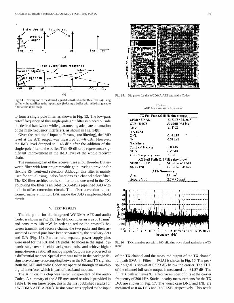
The die photo for the integrated WCDMA AFE and audioCodec is shown in Fig. 15. The AFE occupies an area of 15 mmand consumes 148 mW. In order to reduce the crosstalk be-tween transmit and receive chains, the two paths and their as-sociated external pins have been separated by the auxiliary A/Dand D/A (Fig. 15). Furthermore, separate power-supply pinswere used for the RX and TX paths. To increase the signal dy-namic range over the chip background noise and achieve highersignal-to-noise ratio, all analog inputs/outputs are processed ina differential manner. Special care was taken in the package de-sign to avoid any crosscoupling between the RX and TX signals.Both the AFE and audio Codec are operated through an on-chipdigital interface, which is part of baseband modem.
The AFE on this chip was tested independent of the audioCodec. A summary of the AFE measured results is provided inTable I. To our knowledge, this is the first published results fora WCDMA AFE. A 300-kHz sine wave was applied to the input
Fig. 15. Die photo for the WCDMA AFE and audio Codec.
TABLE IAFE PERFORMANCESUMMARY
Fig. 16. TX channel output with a 300-kHz sine wave signal applied at the TXinput.
of the TX channel and the measured output of the TX channelfull path (D/A Filter PGA) is shown in Fig. 16. The peakspur signal is shown at 63.23 dB below the carrier. The THDof the channel full-scale output is measured at61.87 dB. Thefull TX path achieves 9.1 effective number of bits at the carrierfrequency of 300 kHz. Static linearity measurements for the TXD/A are shown in Fig. 17. The worst case DNL and INL aremeasured at 0.44 LSB and 0.60 LSB, respectively. This result

780 IEEE JOURNAL OF SOLID-STATE CIRCUITS, VOL. 38, NO. 5, MAY 2003
Fig. 17. Plot of the measured TX D/A. (a) DNL. (b) INL.
Fig. 18. Measured TX filter response across the entire turning range. Darkcurve highlights the measured response after calibration.
Fig. 19. Measured PGA offset during the calibration process.
translates to a near ideal 10-bit D/A performance without theuse of trimming or calibration. Thus demonstrating the designrobustness of the segmented R-2R topology and random-walktechnique. On the dynamic side, the D/A settling time is mea-sured at 51.2 ns.
The TX filter frequency response across the entire tuningrange is shown in Fig. 18. The filter tuning bits were manuallyvaried in single steps from all 0’s to all 1’s and the results wererecorded. The measured cutoff frequency varied from 2.43 to5.62 MHz, which is very close to the simulated range (2.50 to6.07 MHz).The single calibrated result is highlighted in Fig. 18,where the cutoff frequency is shown at 3.68 MHz, which is only1.1% away from the 3.72-MHz target. The passband flatness ismeasured below 0.2 dB.
A real-time calibration was done for the PGA to verify theoperation of the autocalibration process. Fig. 19 shows a cap-tured snapshot of the PGA output while the calibration processis converging to the final value. Note that at the start of the cal-ibration process, the offset of the TX differential outputs mea-sures 235 mV. After the process self-terminates, the correctedoffset voltage is measured at6 mV.
VI. CONCLUSION
The AFE chip described in this work was first-time func-tional. Given such a complex chip, this success was attributedto the use of comprehensive mixed-signal validation before thechip tapeout. After extensive testing, the performance of themajority of the blocks was shown to exceed the required speci-fications. The effect of crosstalk was not observed between thedifferent parts of the chip due to careful layout planning andpackage pin assignment. All the calibration circuits are shownto converge to the design target after the chip is powered on.
ACKNOWLEDGMENT
The authors would like to thank all the members of the Chan-dler Analog Development Center for their contribution to the de-sign, layout, development, and test of this AFE, and the CCD-Iteam for provision of system level specifications and their con-tinuous support throughout the development. Special thanks goto the Technology Development team for the delivery of supe-rior first-time silicon, and the analog CAD team in CCE for theirgreat support on silicon models and CAD environment.
REFERENCES
[1] C. Wong, “A 3-V GSM baseband transmitter,”IEEE J. Solid-State Cir-cuits, vol. 34, pp. 725–730, May 1999.
[2] A. Fraval and F. Dell’ova, “A 10-bit 70-MHz 3.3-V CMOS 0.5-�m D/Aconverter for video applications,”IEEE Trans. Consumer Electron., vol.41, pp. 875–879, Aug. 1995.
[3] J. Fournier and P. Senn, “A 130-MHz 8-bit CMOS video DAC for HDTVapplications,”IEEE J. Solid-State Circuits, vol. 26, pp. 1073–1077, Dec.1991.
[4] L. Wang, Y. Fukatsu, and K. Watanabe, “A CMOS R-2R ladderdigital-to-analog converter and its characterization,” inProc. IEEEInstrumentation and Measurement Technology Conf., May 2001, pp.1026–1031.
[5] G. Van der Plaset al., “A 14-bit intrinsic accuracy Q2 random walkCMOS DAC,” IEEE J. Solid-State Circuits, vol. 34, pp. 1708–1718,Dec. 1999.
[6] A. Durham, W. Redman-White, and J. Hughes, “High-linearity contin-uous-time filter in 5-V VLSI CMOS,”IEEE J. Solid-State Circuits, vol.27, pp. 1270–1276, Sept. 1992.
[7] E. Baguleyet al., Reference Data for Radio Engineers. New York:Sams, 1975.
[8] Hughes, “Analog techniques for very large scale integration,” Ph.D.dissertation, Southampton Univ., Southampton, U.K., 1992.
[9] K. R. Lakshmikumaret al., “Baseband codec for digital cellular tele-phony,”IEEE J. Solid-State Circuits, vol. 26, pp. 1951–1958, Dec. 1991.
Waleed Khalil was born in Cairo, Egypt, in 1968.He received the B.S. and M.S. degrees in electricalengineering from the University of Minnesota, Min-neapolis, in 1992 and 1993, respectively.
He joined Intel Corporation, Chandler, AZ,in 1993, where he worked on CMOS sensors,high-speed memory, and data converters. He was theTechnical Leader for the WCDMA AFE project. Heis currently working on frequency synthesizers forRF applications.

KHALIL et al.: HIGHLY INTEGRATED ANALOG FRONT-END FOR 3G 781
Tsung-Yuan Changreceived the B.Sc. degree fromTatung Institute of Technology, Taipei, Taiwan,R.O.C., the M.S. degree from Syracuse University,Syracuse, NY, and the Ph.D. degree from The OhioState University, Columbus, in 1988, 1992, and1998, respectively, all in electrical engineering.
In 1999, he joined Lucent Technology, Columbus,OH, where he was involved in the testing of cellularbase stations. In 2000, he joined Intel Corporation,Chandler, AZ, to develop CMOS-based analogtransceiver circuits for cellular handsets. He has two
patents pending.
Xuewen Jiang received the B.S. and M.S. degreesin materials science from Shanghai Jiao Tong Uni-versity, Shanghai, China, in 1994 and 1997, respec-tively, and the M.S. and Ph.D. degrees in electricalengineering from the University of Minnesota, Min-neapolis-St. Paul, in 1999 and 2001, respectively.
He has been with Intel Corporation, Chandler,AZ, since 2000. His research interests includeMEMS devices fabrication techniques, digitalreadout electronics for solid-state sensing devices,high-speed data conversion circuitry, and VLSI
current-mode testing.
Syed R. Naqvi was born in Karachi, Pakistan, in1965. He received the B.S degree in electrical en-gineering from NED University of Engineering andTechnology, Karachi, in 1989 and the M.S. degreein electrical engineering from the Arizona StateUniversity, Tempe, in 1993, where he is currentlyworking toward the Ph.D. degree in RF circuits.
He is currently a Staff RF/Analog Engineer forthe Wireless Communication and Computing group,Intel Corporation, Chandler, AZ. His researchinterests include digital module design, clocking,
frequency dividers, bandgaps, and D/A and modulator design.
Babak Nikjou was born in Tehran, Iran, in 1963. Hereceived the B.S. and M.S. degrees in electrical en-gineering from Arizona State University, Tempe, in1986 and 1989, respectively, where he is currentlyworking toward the Ph.D. degree in the area of RFcircuits.
He is currently the Analog Design Manager forthe Wireless Communication and Computing group,Intel Corporation, Chandler, AZ. His researchinterests include CMOS sensors, high-speed cachememory design, and mixed-signal validation.
James Tseng was born in Changhua, Taiwan,R.O.C., in 1976. He received the B.S. and M.S.E.degrees in electrical engineering from Arizona StateUniversity, Tempe, in 1998 and 1999, respectively.
Since 2000, he has been with Intel Corporation,Chandler, AZ, working on developing data convertersand other mixed-signal blocks for use in cell phones.

专注于微波、射频、天线设计人才的培养 易迪拓培训 网址:http://www.edatop.com
射 频 和 天 线 设 计 培 训 课 程 推 荐
易迪拓培训(www.edatop.com)由数名来自于研发第一线的资深工程师发起成立,致力并专注于微
波、射频、天线设计研发人才的培养;我们于 2006 年整合合并微波 EDA 网(www.mweda.com),现
已发展成为国内最大的微波射频和天线设计人才培养基地,成功推出多套微波射频以及天线设计经典
培训课程和 ADS、HFSS 等专业软件使用培训课程,广受客户好评;并先后与人民邮电出版社、电子
工业出版社合作出版了多本专业图书,帮助数万名工程师提升了专业技术能力。客户遍布中兴通讯、
研通高频、埃威航电、国人通信等多家国内知名公司,以及台湾工业技术研究院、永业科技、全一电
子等多家台湾地区企业。
易迪拓培训课程列表:http://www.edatop.com/peixun/rfe/129.html
射频工程师养成培训课程套装
该套装精选了射频专业基础培训课程、射频仿真设计培训课程和射频电
路测量培训课程三个类别共 30 门视频培训课程和 3 本图书教材;旨在
引领学员全面学习一个射频工程师需要熟悉、理解和掌握的专业知识和
研发设计能力。通过套装的学习,能够让学员完全达到和胜任一个合格
的射频工程师的要求…
课程网址:http://www.edatop.com/peixun/rfe/110.html
ADS 学习培训课程套装
该套装是迄今国内最全面、最权威的 ADS 培训教程,共包含 10 门 ADS
学习培训课程。课程是由具有多年 ADS 使用经验的微波射频与通信系
统设计领域资深专家讲解,并多结合设计实例,由浅入深、详细而又
全面地讲解了 ADS 在微波射频电路设计、通信系统设计和电磁仿真设
计方面的内容。能让您在最短的时间内学会使用 ADS,迅速提升个人技
术能力,把 ADS 真正应用到实际研发工作中去,成为 ADS 设计专家...
课程网址: http://www.edatop.com/peixun/ads/13.html
HFSS 学习培训课程套装
该套课程套装包含了本站全部 HFSS 培训课程,是迄今国内最全面、最
专业的HFSS培训教程套装,可以帮助您从零开始,全面深入学习HFSS
的各项功能和在多个方面的工程应用。购买套装,更可超值赠送 3 个月
免费学习答疑,随时解答您学习过程中遇到的棘手问题,让您的 HFSS
学习更加轻松顺畅…
课程网址:http://www.edatop.com/peixun/hfss/11.html
`

专注于微波、射频、天线设计人才的培养 易迪拓培训 网址:http://www.edatop.com
CST 学习培训课程套装
该培训套装由易迪拓培训联合微波 EDA 网共同推出,是最全面、系统、
专业的 CST 微波工作室培训课程套装,所有课程都由经验丰富的专家授
课,视频教学,可以帮助您从零开始,全面系统地学习 CST 微波工作的
各项功能及其在微波射频、天线设计等领域的设计应用。且购买该套装,
还可超值赠送 3 个月免费学习答疑…
课程网址:http://www.edatop.com/peixun/cst/24.html
HFSS 天线设计培训课程套装
套装包含 6 门视频课程和 1 本图书,课程从基础讲起,内容由浅入深,
理论介绍和实际操作讲解相结合,全面系统的讲解了 HFSS 天线设计的
全过程。是国内最全面、最专业的 HFSS 天线设计课程,可以帮助您快
速学习掌握如何使用 HFSS 设计天线,让天线设计不再难…
课程网址:http://www.edatop.com/peixun/hfss/122.html
13.56MHz NFC/RFID 线圈天线设计培训课程套装
套装包含 4 门视频培训课程,培训将 13.56MHz 线圈天线设计原理和仿
真设计实践相结合,全面系统地讲解了 13.56MHz线圈天线的工作原理、
设计方法、设计考量以及使用 HFSS 和 CST 仿真分析线圈天线的具体
操作,同时还介绍了 13.56MHz 线圈天线匹配电路的设计和调试。通过
该套课程的学习,可以帮助您快速学习掌握 13.56MHz 线圈天线及其匹
配电路的原理、设计和调试…
详情浏览:http://www.edatop.com/peixun/antenna/116.html
我们的课程优势:
※ 成立于 2004 年,10 多年丰富的行业经验,
※ 一直致力并专注于微波射频和天线设计工程师的培养,更了解该行业对人才的要求
※ 经验丰富的一线资深工程师讲授,结合实际工程案例,直观、实用、易学
联系我们:
※ 易迪拓培训官网:http://www.edatop.com
※ 微波 EDA 网:http://www.mweda.com
※ 官方淘宝店:http://shop36920890.taobao.com
专注于微波、射频、天线设计人才的培养
官方网址:http://www.edatop.com 易迪拓培训 淘宝网店:http://shop36920890.taobao.com