a ka tt - college of...
TRANSCRIPT

1
MSE 510
Knowlton 1
Part 5: Quantum Effects in MOS Devices
Quantum Effects Lead to Phenomena such as:Ultra Thin Oxides – Observe:
High Leakage Currents Through the Oxide - TunnelingDepletion in Poly-Si metal gate – capacitance effectThickness of Inversion Layer – alters tox
GIDL (Gate-Induced Drain Leakage) – High Doping - Leads to tunnelingDIBL (Drain-Induced Barrier Lowering) – Short Channel - Leads to tunneling
Take advantage of Quantum EffectsDecrease effective mass
Change E -vs- k energy band diagram by…Induce strain using lattice mismatch between S/Cs
Quantum Confinement – Gain in Device EfficiencyBand gap engineering – Use other S/Cs to decrease Eg
MSE 510
Knowlton 2
Part 5: Quantum Effects in MOS Devices
Ultrathin SiO2 – begin to observe quantum effects
o r o oxox
ox ox
A k AC
t t
Crystalline Si
poly-crystallineSi
p-Si Wafer
Insulator InsulatorSiO2 - Gate oxide
Source Contact Drain Contactn++ Poly Si
Gate Contact or Electrode
n+source n+drain
+
+Vgate
VDrain
channel- - -- - - -- - -- - - -
M
O
S
VSource
L
W
tox
2
MSE 510
Knowlton 3
SiO2
p- Si
Ef
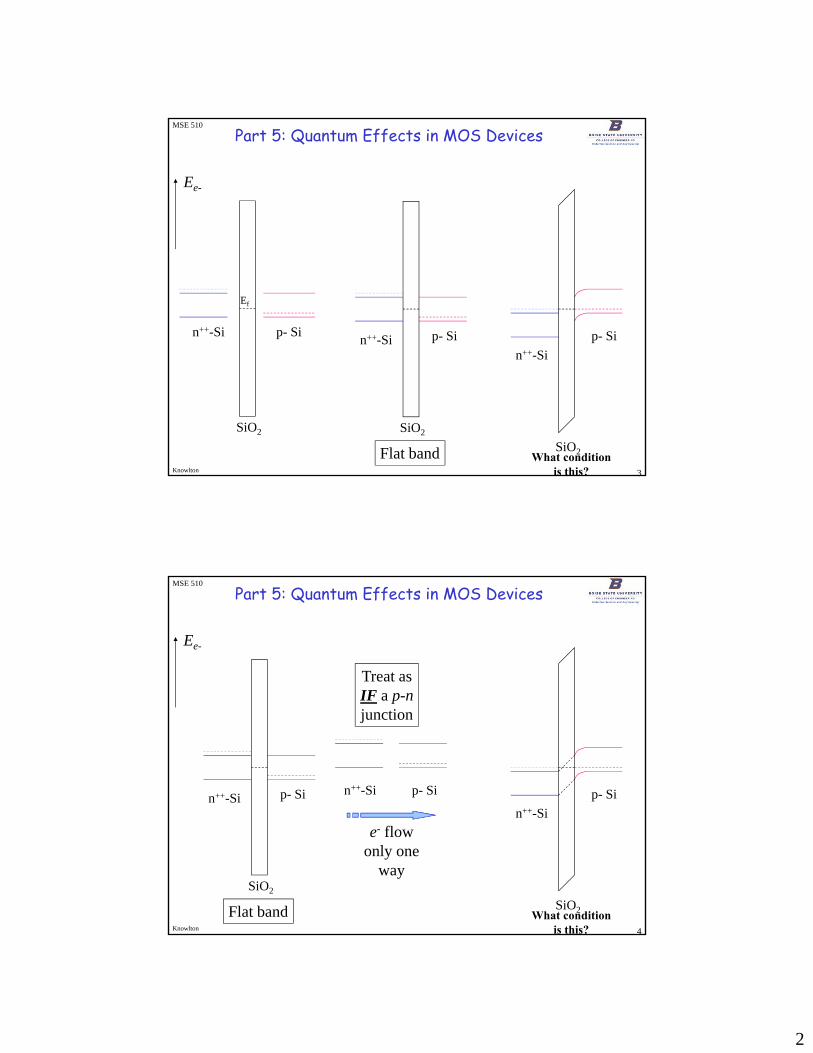
Part 5: Quantum Effects in MOS Devices
Ee-
n++-Si
SiO2
Flat band
p- Sin++-Si
SiO2
p- Si
n++-Si
What conditionis this?
MSE 510
Knowlton 4
Part 5: Quantum Effects in MOS Devices
Ee-
SiO2
Flat band
p- Sin++-Si
SiO2
p- Si
n++-Si
What conditionis this?
Treat asIF a p-njunction
n++-Si p- Si
e- flowonly one
way
3
MSE 510
Knowlton 5
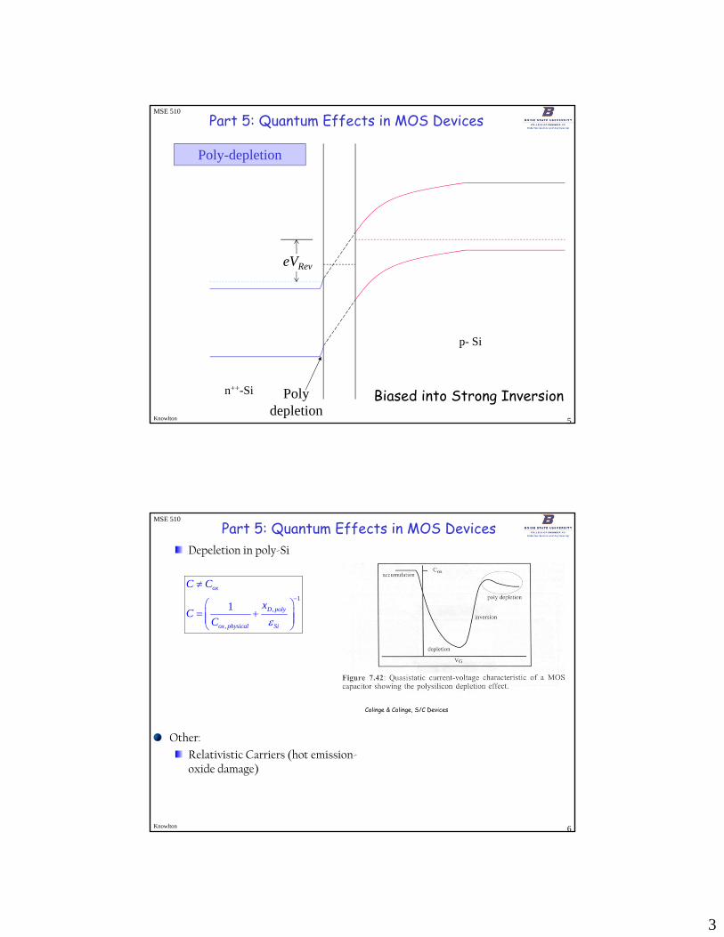
Part 5: Quantum Effects in MOS Devices
n++-Si
p- Si
Polydepletion
Poly-depletion
Biased into Strong Inversion
eVRev
MSE 510
Knowlton 6
Part 5: Quantum Effects in MOS DevicesDepeletion in poly-Si
Other:
Relativistic Carriers (hot emission-oxide damage)
1
,
,
1
ox
D poly
ox physical Si
C C
xC
C
Colinge & Colinge, S/C Devices

4
MSE 510
Knowlton 7
Part 5: Quantum Effects in MOS DevicesQuantization: (cont.)
2D gas in channelInversion layer thickness is similar to the gate oxide thickness
Changes oxide thickness, ,
oxox eff ox physical
Si
t t x
Hareland, IEEE Transactions on Electron Devices, 1996
See also:Anderson & Anderson. Fundamentals of Semiconductor Devices, (McGraw Hill, 2005) p. 504-506
Davies, The Physics of Low Dimensional Semiconductors, (Cambridge, 1998) p. 343
MSE 510
Knowlton 8
Part 5: Quantum Effects in MOS DevicesQuantization (Cont.) – Consider Quantization in MOS Channel
From Principles of Electronic Materials and Devices, Third Edition, S.O. Kasap (© McGraw-Hill, 2005)
EC,S-C
Oxide
Semiconductor
Ee-
Where are:Ψ and lΨl2located???
5
MSE 510
Knowlton 9
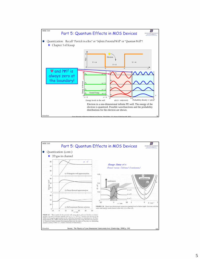
Part 5: Quantum Effects in MOS Devices
Quantization: Recall “Particle in a Box” or “Infinite Potential Well” or “Quantum Well”?Chapter 3 of Kasap
x = 0 x = a0
E1
E3
E2
E4
n = 1
n = 2
n = 3
n = 4
Ener
gyof
elec
tron
Energy levels in the well (x) sin(nx/a) Probability density |(x)|2
1
2
3
4
0 a a0
x
0 a x0
V(x
)
V = 0
Electron
V = 8 V = 8
Electron in a one-dimensional infinite PE well. The energy of theelectron is quantized. Possible wavefunctions and the probabilitydistributions for the electron are shown.
8
From Principles of Electronic Materials and Devices, Third Edition, S.O. Kasap (© McGraw-Hill, 2005)
Ψ and lΨl2 is always zero at the boundary!
MSE 510
Knowlton 10
Part 5: Quantum Effects in MOS DevicesQuantization: (cont.)
2D gas in channelInversion layer thickness is similar to the gate oxide thickness
Changes oxide thickness
, ,ox
ox eff ox physicalSi
t t x
Davies, The Physics of Low Dimensional Semiconductors, (Cambridge, 1998) p. 343
n ~1Energy States of e-:
Bound versus Unbound (continuum)

6
MSE 510
Knowlton 11
Part 5: Quantum Effects in MOS DevicesTunneling:
Fowler-Nordheim (FN) [cold emission – oxides]
Direct (oxides)
Band-to-Band
Barrier lowering
Drain Induced Barrier Lowering (DIBL)
Muller & Kamins (Wiley-Interscience,2003) Fig. 9.17 p. 452Streetman & Banerjee , Solid State Electronic Circuits (Prentice Hall,2000)
This results because…
…this occurs.
p-Si Wafer
SiO2 - Gate oxide
DrainContact
Poly SiGate Contact
n+source n+drain
VdVg
Vgate= On VD=VDD
channel
DrainContact
MSE 510
Knowlton 12
Part 5: Quantum Effects in MOS DevicesTunneling:
Fowler-Nordheim (FN) [cold emission – oxides]
Direct (oxides)
Band-to-Band
Barrier lowering
GIDL Sze, Modern S/C Device Physics (Wiley-Interscience,1998)Ch. 3 by SlJ. Hillenius
P-Si Wafer
SiO2 - Gate oxide
DrainContact
Poly SiGate Contact
n+source n+drain
VdVg
Vgate=0 VD=VDD
channel
DrainContact
Gate Induced Drain Leakage (GIDL)
Colinge & Colinge, S/
C Devices
7
MSE 510
Knowlton 13
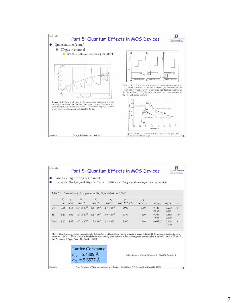
Part 5: Quantum Effects in MOS DevicesQuantization: (cont.)
2D gas in channelSOI Gate-all-around (GAA) MOSFET:
Colinge & Colinge, S/C Devices
MSE 510
Knowlton 14
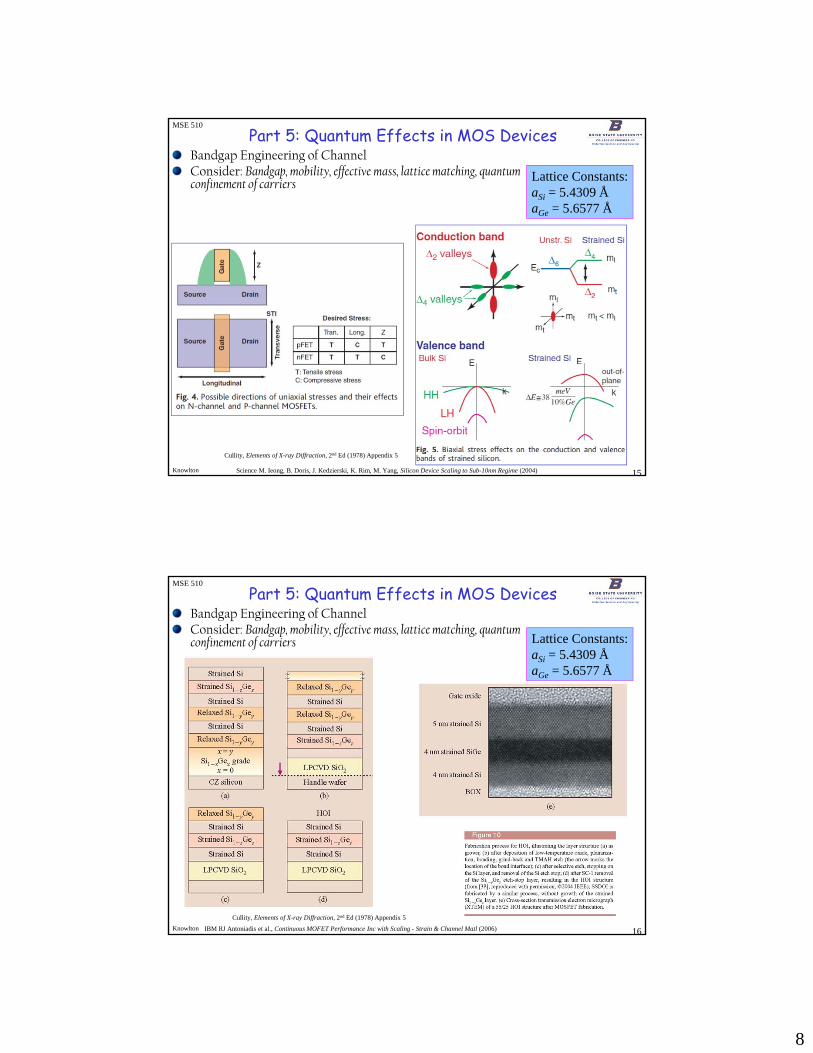
Part 5: Quantum Effects in MOS DevicesBandgap Engineering of ChannelConsider: Bandgap, mobility, effective mass, lattice matching, quantum confinement of carriers
From Principles of Electronic Materials and Devices, Third Edition, S.O. Kasap (© McGraw-Hill, 2005)
Lattice Constants:aSi = 5.4309 ÅaGe = 5.6577 Å
Cullity, Elements of X-ray Diffraction, 2nd Ed (1978) Appendix 5
8
MSE 510
Knowlton 15
Part 5: Quantum Effects in MOS DevicesBandgap Engineering of ChannelConsider: Bandgap, mobility, effective mass, lattice matching, quantum confinement of carriers
Science M. Ieong, B. Doris, J. Kedzierski, K. Rim, M. Yang, Silicon Device Scaling to Sub-10nm Regime (2004)
Lattice Constants:aSi = 5.4309 ÅaGe = 5.6577 Å
Cullity, Elements of X-ray Diffraction, 2nd Ed (1978) Appendix 5
MSE 510
Knowlton 16
Part 5: Quantum Effects in MOS DevicesBandgap Engineering of ChannelConsider: Bandgap, mobility, effective mass, lattice matching, quantum confinement of carriers
IBM RJ Antoniadis et al., Continuous MOFET Performance Inc with Scaling - Strain & Channel Matl (2006)
Lattice Constants:aSi = 5.4309 ÅaGe = 5.6577 Å
Cullity, Elements of X-ray Diffraction, 2nd Ed (1978) Appendix 5
9
MSE 510
Knowlton 17
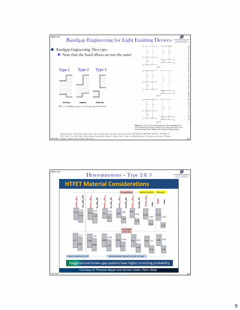
Bandgap Engineering for Light Emitting Devices
Bandgap Engineering: Three typesNote that the band offsets are not the same!
Herbert Kroemer, Nobel Lecture: Quasielectric fields and band offsets: teaching electrons new tricks*, REVIEWS OF MODERN PHYSICS, VOLUME 73, JULY 2001, *The 2000 Nobel Prize in Physics was shared by Zhores I. Alferov, Jack S. Kilby, and Herbert Kroemer. This lecture is the text of Professor Kroemer’s address on the occasion of the award.
Anderson &
Anderson, Fundam
entals of Semiconductor D
evices, (McG
raw H
ill, 2005) Ch. 6.3 p. 317-331
Type 1 Type 2 Type 3
MSE 510
Knowlton
Heterojunctions – Type 2 & 3
18
10
MSE 510
Knowlton
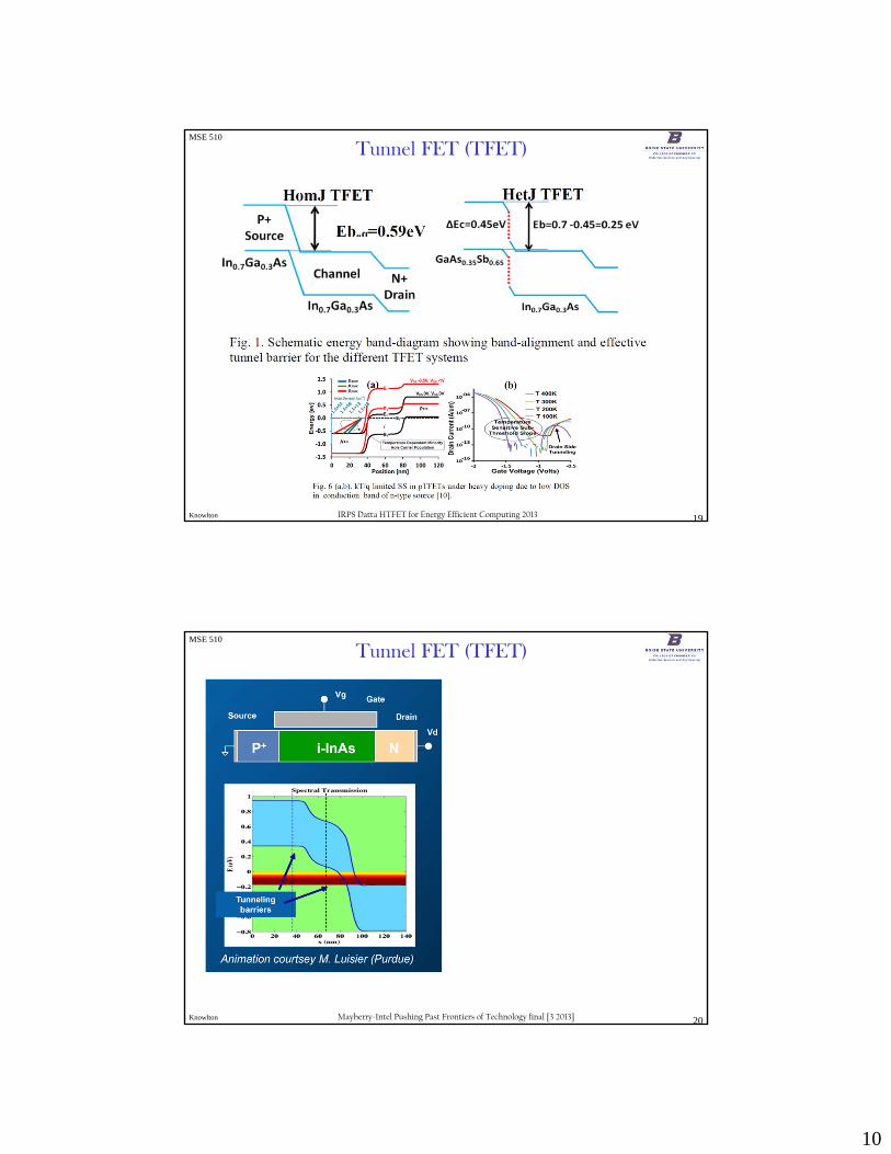
Tunnel FET (TFET)
19IRPS Datta HTFET for Energy Efficient Computing 2013
MSE 510
Knowlton
Tunnel FET (TFET)
20Mayberry-Intel Pushing Past Frontiers of Technology final [3 2013]
11
MSE 510
Knowlton 21
Part 5: Quantum Effects in MOS Devices
Quantization: (cont.)
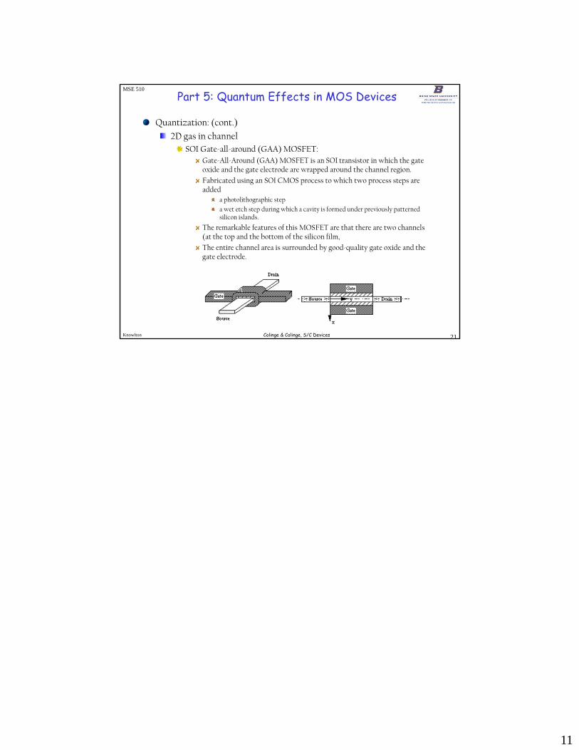
2D gas in channelSOI Gate-all-around (GAA) MOSFET:
Gate-All-Around (GAA) MOSFET is an SOI transistor in which the gate oxide and the gate electrode are wrapped around the channel region.
Fabricated using an SOI CMOS process to which two process steps are added
a photolithographic step
a wet etch step during which a cavity is formed under previously patterned silicon islands.
The remarkable features of this MOSFET are that there are two channels (at the top and the bottom of the silicon film,
The entire channel area is surrounded by good-quality gate oxide and the gate electrode.
Colinge & Colinge, S/C Devices