a low dropout voltage regulator with a transient voltage spikes...
TRANSCRIPT

Turk J Elec Eng & Comp Sci(2020) 28: 500 – 508© TÜBİTAKdoi:10.3906/elk-1904-203
Turkish Journal of Electrical Engineering & Computer Sciences
http :// journa l s . tub i tak .gov . t r/e lektr ik/
Research Article
A low dropout voltage regulator with a transient voltage spikes reducer andimproved figure of merit
Guru PRASAD∗, Kumara SHAMADepartment of Electronics and Communication, Manipal Institute of Technology,
Manipal Academy of Higher Education, Manipal, India Prasad
Received: 29.04.2019 • Accepted/Published Online: 11.09.2019 • Final Version: 27.01.2020
Abstract: An area efficient output capacitor-free low dropout [LDO] voltage regulator with an improved figure of meritis presented in this paper. The proposed LDO regulator consists of a novel, dynamically biased error amplifier thatreduces overshoot and undershoot voltage spikes arising from abrupt load changes. Source bulk modulation is employedto enhance the current driving capability of the pass transistor. An adaptive biasing scheme is also used along withdynamic biasing to improve the current efficiency of the system. The on-chip capacitor required for proper working ofthe LDO regulator is only 35 pF. The proposed LDO regulator is designed and simulated in 180 nm standard CMOStechnology. The LDO regulator exhibits a line regulation of 1.67 mV/V and a load regulation of 100 µV/mA. Whenload changes from 0 mA to 100 mA in 1 µs, an undershoot of 148 mV and an overshoot of 172 mV are observed. Themeasured power supply rejection ratio is 25 dB at 100 kHz. The working of the proposed LDO regulator has been testedunder all process corners and Monte-Carlo statistical analysis reveals that it is robust against process variations andlocal mismatch.
Key words: Dynamic biasing, adaptive biasing, source bulk modulation, output capacitorless, figure of merit, lowdropout voltage regulator
1. IntroductionToday’s electronics market is dominated by battery operated devices. These devices need integrated powermanagement circuits to meet the desired requirements. A typical power management system consists ofswitching regulators, linear regulators, voltage references, etc. Low dropout (LDO) regulators belong to thelinear regulator category, which has better power efficiency, transient response, and noise immunity.
An LDO regulator is basically a negative feedback system in which the resistivity of the pass device iscontrolled by an error amplifier such that a constant voltage difference is maintained between input and outputterminals even though there are fluctuations in supply voltage and load demand [1–3]. The vital performanceindicators of LDO regulators are line and load regulation, maximum load current, transient response, on-chipcapacitance value, stability, quiescent current magnitude, and power supply rejection ratio [PSRR] [4, 5]. It ispractically impossible to improve all the parameters together. For example, if the quiescent current is reduced,transient response is hampered. Hence, a figure of merit [FOM ] quantity is defined, which is a collective measureof the above-mentioned parameters. The objective of many recent LDO regulators has been to improve thisFOM. Equation (1) defines the FOM used in [6, 7] and the smaller the FOM value, the better the performance.∗Correspondence: [email protected]
This work is licensed under a Creative Commons Attribution 4.0 International License.500

PRASAD and SHAMA/Turk J Elec Eng & Comp Sci
FOM =Cout ×∆Vpeak × IQ
I2o,max
, (1)
where Cout is the output capacitance used in the design for stability and better transient response. ∆Vpeak isthe voltage spike observed when load current changes from minimum to maximum. IQ is the quiescent currentunder no load condition. Io,max is the maximum load supplied by the LDO regulator.
Recently many have proposed different LDO regulator architectures and design techniques to improveFOM [7–11]. In [12] a local common mode feedback technique was used to increase the order of transfercharacteristics, so that at low quiescent current better regulation could be achieved. However, while the lineand load regulation were improved, the voltage spike during load transition was high. The author of [13]proposed an LDO regulator with small gain stages in which load was distributed between two pass transistorsand on-chip capacitance was avoided. However, the observed line and load regulation were poor. A nestedMiller capacitor-based LDO regulator was presented in [14]. Line and load regulation and transient responseswere improved significantly but occupied a large area on the chip. A flipped voltage follower output stagewas used in [15] to improve the response time and reduce the voltage spike during load transition. However,the LDO regulator was able to deliver only 10 mA load. Another design technique to improve the transientresponse is to use multiple loops with different loop delays. Although this was adapted in [16], the achievedFOM value was very high. Better transient response can be achieved even with low quiescent current by havinga dedicated voltage spike detection circuit that increases the quiescent current momentarily only when required.The author of [17] implemented this technique, and although the transient response was improved, the on-chipcapacitor used was large and maximum driving load current was very low. The present work tries to improveFOM by adapting a novel dynamic biasing technique along with an adaptive biasing scheme and source bulkmodulation. On-chip capacitance is kept very low so that area occupancy is significantly reduced. The restof the article is arranged as follows. The structure and working principle of the proposed LDO regulator areexplained in section 2. Stability analysis of the LDO regulator is outlined in section 3. The simulation resultsand discussion are elaborated in section 4. The conclusion is drawn in the last section.
2. Structure and operation of the proposed LDO regulatorThe objective of the proposed LDO regulator is to improve the figure of merit and reduce the area occupancy.The area occupied by the LDO largely depends on the size of the on-chip capacitor. If the capacitance value isreduced to minimize the area, then transient response and stability are degraded. At the same time, to improvethe FOM, quiescent current [IQ ] and voltage spikes during abrupt load transition have to be reduced. Hence,the main focus is to improve transient response without using a large IQ . Large IQ is required only duringabrupt load change and also the magnitude of IQ should vary proportionately with respect to the magnitude ofload current. Dynamic biasing addresses the former issue, whereas the adaptive biasing takes care of the latter.One more factor that affects the transient response is the large parasitic capacitance present at the gate of thepass transistor. This large size of parasitic capacitance is due to the large size of the pass transistor, which isrequired to accommodate minimum dropout voltage and maximum output current. The MOSFET source bulkmodulation technique can reduce the threshold voltage so that the size of the pass transistor and associatedparasitic capacitance can be reduced.
Figure 1 shows the schematic diagram of the proposed LDO regulator. Transistors from M1 to M9 forman error amplifier, which is basically an operational transconductance amplifier [OTA]. M5a , M10 , R3 , C3 ,
501

PRASAD and SHAMA/Turk J Elec Eng & Comp Sci
and Ib1 constitute the undershoot voltage spike reducer block. M5b , M11 , M12 ,M13 , R4 , C4 , and Ib2 arepart of the overshoot voltage spike reducer circuit. When output voltage suddenly drops due to a steep changein the load, C3 and R3 act as differentiator and |VGS | of M5a momentarily increases, which provides large IQ
to charge parasitic capacitance; hence undershoot voltage is reduced. During this, the overshoot voltage spikereducer circuit will be in cut-off mode. Similarly, only the overshoot reducer is active during the overshootof output voltage and reduces the voltage spike. The current mirror formed by M14 and M15 maintains thesame drain voltage across the main pass transistor Mp and auxiliary pass transistor Mpa . The transistor pairM16 and M17 adaptively varies the bias point of the Schottky diode D1 with respect to load current. In thisway the magnitude of IQ is controlled by the load current. The Schottky diode can be realized in standardCMOS technology [18]. Transistor M18 acts as a current buffer during instantaneous load transition. Whenload changes from minimum to maximum in a short period, voltages at the output and at the gate of M18 drop,forcing M18 to draw less current. In the meantime, the pass transistor steers this current to the output node.Hence, there is an improvement in transient response.
Table 1 shows the W/L ratio of all the MOSFETs and the values of passive components and bias currentsused in the LDO regulator.
M1 M2
M3 M4
M5a M5b
M6
M9
M10 M11
M7
M8
M12
M13
Mpa Mp
M14 M15
M16 M17
M18
R3
R4
R1
R2
Ib1
Ib2
Ib3
D1
Vref
Vout
Vin
Unit
Current
Buffer
C1 C2C3
C4
OTA
Undershoot
Spike Reducer Spike Reducer
Overshoot Pass Transistor
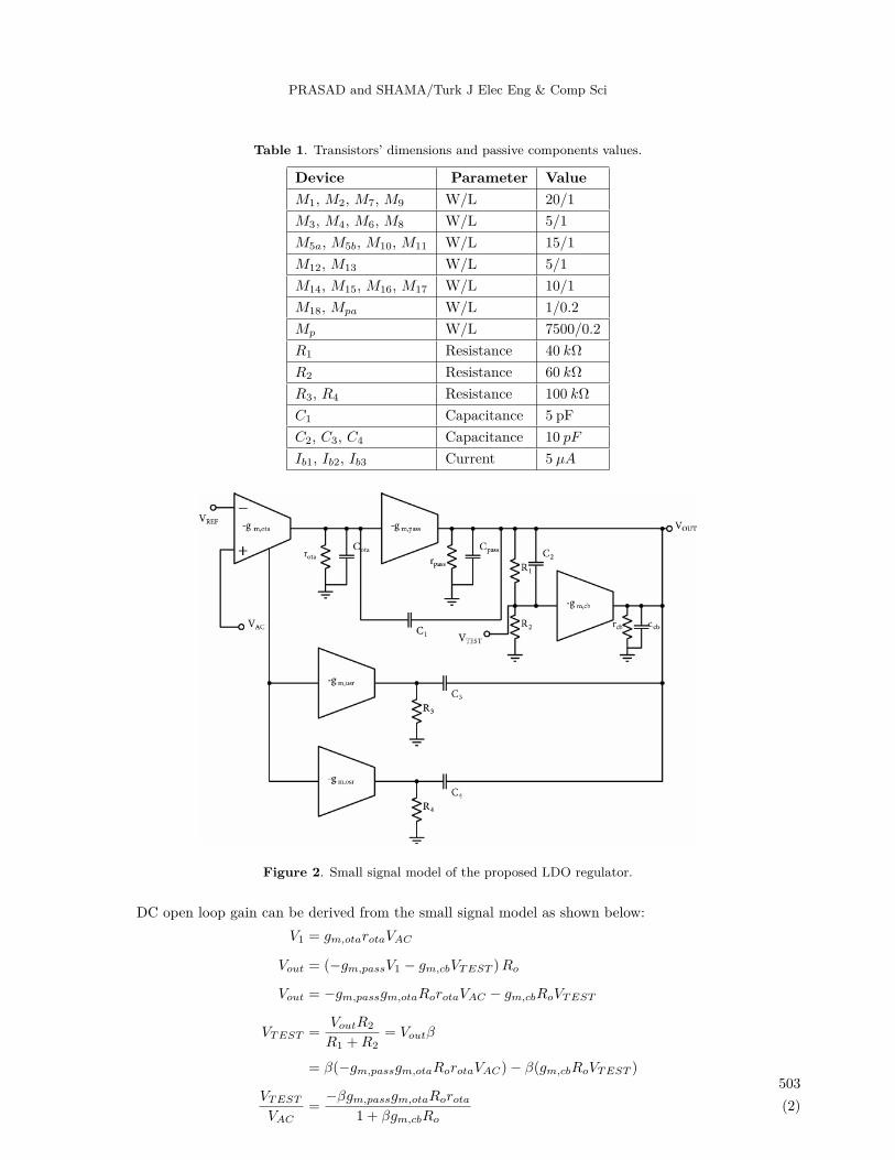
Figure 1. Schematic of the proposed LDO regulator.
3. Stability Analysis
Figure 2 shows the simplified small signal model of the proposed LDO regulator, wheregm,ota , gm,cb → Transconductance of the OTA and current buffer transistor (M18) .gm,pass → Total transconductance of the pass transistor.gm,usr , gm,osr → Transconductance of the undershoot spike reducer block and overshoot spike reducer block.rota , rpass and rcb → Output resistance of the OTA, pass transistor, and M18
Cota , Cpass and Ccb → Parasitic capacitance of the OTA, pass transistor, and M18
Ro = rpass ∥ rcb ∥ (R1 +R2) → Total output resistance.CE1 = Cota + C1(1 + gm,passRo) → Effective capacitance at output of OTA.CE2 = Cpass+C1 + Ccb → Effective capacitance at the output of the pass transistor.
502
PRASAD and SHAMA/Turk J Elec Eng & Comp Sci
Table 1. Transistors’ dimensions and passive components values.
Device Parameter ValueM1, M2, M7, M9 W/L 20/1M3, M4, M6, M8 W/L 5/1M5a, M5b, M10, M11 W/L 15/1M12, M13 W/L 5/1M14, M15, M16, M17 W/L 10/1M18, Mpa W/L 1/0.2Mp W/L 7500/0.2R1 Resistance 40 kΩ
R2 Resistance 60 kΩ
R3, R4 Resistance 100 kΩ
C1 Capacitance 5 pFC2, C3, C4 Capacitance 10 pF
Ib1, Ib2, Ib3 Current 5 µA
Figure 2. Small signal model of the proposed LDO regulator.
DC open loop gain can be derived from the small signal model as shown below:V1 = gm,otarotaVAC
Vout = (−gm,passV1 − gm,cbVTEST )Ro
Vout = −gm,passgm,otaRorotaVAC − gm,cbRoVTEST
VTEST =VoutR2
R1 +R2= Voutβ
= β(−gm,passgm,otaRorotaVAC)− β(gm,cbRoVTEST )
VTEST
VAC=
−βgm,passgm,otaRorota1 + βgm,cbRo
(2)503
PRASAD and SHAMA/Turk J Elec Eng & Comp Sci
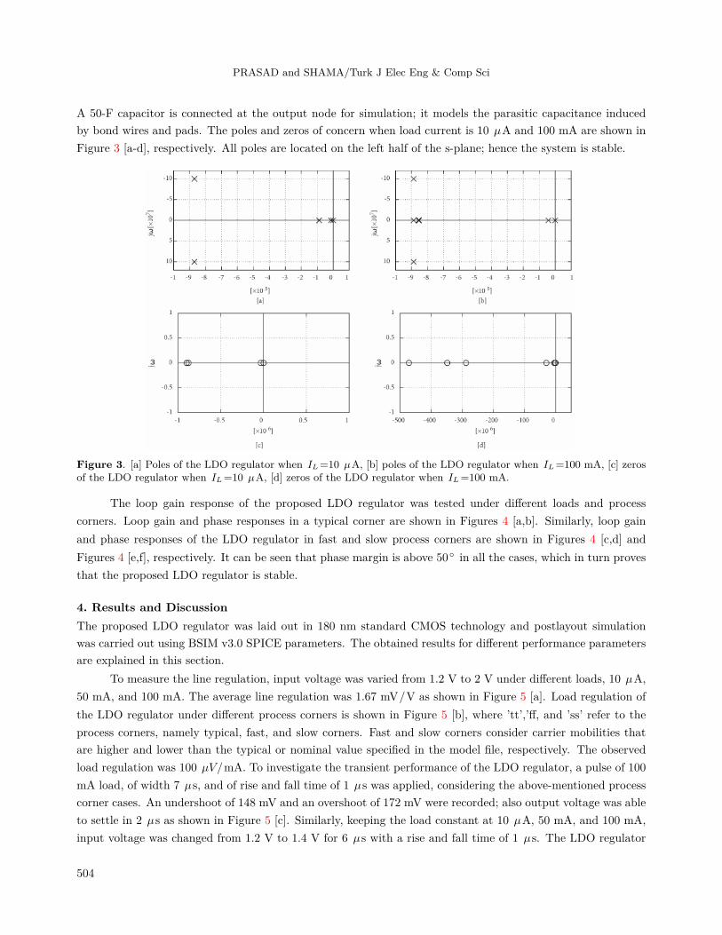
A 50-F capacitor is connected at the output node for simulation; it models the parasitic capacitance inducedby bond wires and pads. The poles and zeros of concern when load current is 10 µA and 100 mA are shown inFigure 3 [a-d], respectively. All poles are located on the left half of the s-plane; hence the system is stable.
Figure 3. [a] Poles of the LDO regulator when IL =10 µA, [b] poles of the LDO regulator when IL =100 mA, [c] zerosof the LDO regulator when IL =10 µA, [d] zeros of the LDO regulator when IL =100 mA.
The loop gain response of the proposed LDO regulator was tested under different loads and processcorners. Loop gain and phase responses in a typical corner are shown in Figures 4 [a,b]. Similarly, loop gainand phase responses of the LDO regulator in fast and slow process corners are shown in Figures 4 [c,d] andFigures 4 [e,f], respectively. It can be seen that phase margin is above 50 in all the cases, which in turn provesthat the proposed LDO regulator is stable.
4. Results and DiscussionThe proposed LDO regulator was laid out in 180 nm standard CMOS technology and postlayout simulationwas carried out using BSIM v3.0 SPICE parameters. The obtained results for different performance parametersare explained in this section.
To measure the line regulation, input voltage was varied from 1.2 V to 2 V under different loads, 10 µA,50 mA, and 100 mA. The average line regulation was 1.67 mV/V as shown in Figure 5 [a]. Load regulation ofthe LDO regulator under different process corners is shown in Figure 5 [b], where ’tt’,’ff, and ’ss’ refer to theprocess corners, namely typical, fast, and slow corners. Fast and slow corners consider carrier mobilities thatare higher and lower than the typical or nominal value specified in the model file, respectively. The observedload regulation was 100 µV/mA. To investigate the transient performance of the LDO regulator, a pulse of 100mA load, of width 7 µs, and of rise and fall time of 1 µs was applied, considering the above-mentioned processcorner cases. An undershoot of 148 mV and an overshoot of 172 mV were recorded; also output voltage was ableto settle in 2 µs as shown in Figure 5 [c]. Similarly, keeping the load constant at 10 µA, 50 mA, and 100 mA,input voltage was changed from 1.2 V to 1.4 V for 6 µs with a rise and fall time of 1 µs. The LDO regulator
504

PRASAD and SHAMA/Turk J Elec Eng & Comp Sci
Figure 4. [a]&[b] Loop gain and phase response-typical corner, [c]&[d] loop gain and phase response-fast corner, [e]&[f]loop gain and phase response-slow corner.
response is shown in Figure 5 [d]. It can be seen that even under full load the voltage spike was within 80 mV.To study the effect of temperature variation, the output voltage was measured for different temperatures
ranging from 0 C to 100 C and typical (tt), fast (ff), and slow (ss) process corners. The LDO regulatoroutput voltage was almost constant as shown in Figure 6 [a]. The PSRR of the LDO regulator is shown inFigure 6 [b]. When load was 100 mA, the PSRR was 25 dB at 100 kHz.
Monte-Carlo statistical analysis was carried out to find the effect of local and global parameter variationson the operation of the designed LDO regulator. Three key performance parameters, line regulation, loadregulation, and undershoot voltage, during load transition were measured in the Monte-Carlo simulation.Threshold voltage and carrier mobility were considered for local mismatch and global variations. Totally 100samples were taken and Gaussian distribution was assumed for varying the parameters. Figure 7 [a] shows thehistogram plot of variation in line regulation for different samples. The mean value of line regulation was 1.51mV/V. Histogram plots of variations in load regulation and undershoot spike voltage during load transitionare shown in Figures 7 [b] and Figure 7 [c], respectively. The mean value of load regulation was 151.2 µV/mA
505

PRASAD and SHAMA/Turk J Elec Eng & Comp Sci
Figure 5. [a] Line regulation of the LDO regulator, [b] load regulation of the LDO regulator, [c] load transient responseof the LDO regulator, [d] line transient response of the LDO regulator.
and undershoot voltage was 160.3 mV. In all three simulations the mean values of parameters match the typicalvalues and also standard deviation was less. This shows that the proposed LDO regulator is robust againstprocess variations and mismatch.The layout of the LDO regulator is depicted in Figure 8. The area occupiedby the LDO regulator was 0.06253 mm2 .
The performance of the proposed LDO regulator has been compared with that of the recent state ofthe art LDO regulators as shown in Table 2. The table reveals that the proposed LDO regulator has a bettercurrent driving capability for the given quiescent current. The on-chip capacitance value of the LDO regulatoris only 35 pF and hence the area occupied by it is very small. FOM is calculated using equation (1). FromTable 2, it is evident that the proposed LDO regulator has the lowest FOM value.
Figure 6. [a] Temperature response of the LDO regulator, [b] PSRR response of the LDO regulator.
506

PRASAD and SHAMA/Turk J Elec Eng & Comp Sci
Figure 7. [a] Histogram plot of line regulation for different samples, [b] histogram plot of load regulation for differentsamples, [c] histogram plot of undershoot voltage for different samples when load changes from 0 mA to 100 mA.
Figure 8. Layout of the LDO regulator.
Table 2. Performance comparison of the proposed LDO regulator with recent LDO regulators.
Parameters [15] [7] [17] [8] [9] [10] [11] [6] Present workTechnology [nm] 65 90 180 350 65 350 350 500 180Vout[V] 0.5 0.9 1.6 1 1 1.6 1 1.8 1Imax[mA] 10 100 50 50 10 12 100 100 100IQ [µA] 49.4 6000 55 95 50 28.6 100 78 65Vdrpout [mV ] 250 300 200 200 150 400 200 200 200∆Vout[mV] 41.6 600 120 180 82 40 50 135 148Con,chip[pF ] 16 100 28 20 140 28 100 100 35FOM [fs] 328.8 36000 73.92 136.8 5740 222.4 50 105.3 33.15
5. ConclusionIn this paper, an output off-chip capacitor-free, area efficient low dropout voltage regulator with improved FOMis presented. A novel dynamic biasing technique has been adapted, from which the LDO regulator is able toexhibit a better transient response without consuming a large quiescent current. With the help of source bulkmodulation, the parasitic capacitance of the pass transistor has been reduced. For proper operation of theLDO regulator, only 35 pF on-chip capacitance is required; hence the area occupancy of the circuit is very low,
507

PRASAD and SHAMA/Turk J Elec Eng & Comp Sci
making it suitable for area constraint applications. Moreover, optimum performance can be achieved with theproposed LDO regulator because of its improved FOM.
References
[1] Rincon-Mora GA, Allen PE. A low-voltage, low quiescent current, low drop-out regulator. IEEE Journal of Solid-State Circuits 1998; 33 (1): 36-44.
[2] Qu X, Zhou ZK, Zhang B, Li ZJ. An ultralow-power fast-transient capacitor-free low-dropout regulator withassistant push–pull output stage. IEEE Transactions on Circuits and Systems II: Express Briefs 2013; 60 (2):96-100.
[3] Esteves J, Pereira J, Paisana J, Santos M. Ultra low power capless LDO with dynamic biasing of derivative feedback.Microelectronics Journal 2013; 44 (2): 94-102.
[4] Patel AP, Rincón-Mora GA. High power-supply-rejection (PSR) current-mode low-dropout (LDO) regulator. IEEETransactions on Circuits and Systems II: Express Briefs 2010; 57 (11): 868-873.
[5] Hong SW, Cho GH. High-gain wide-bandwidth capacitor-less low-dropout regulator (LDO) for mobile applicationsutilizing frequency response of multiple feedback loops. IEEE Transactions on Circuits and Systems I: RegularPapers 2016; 63 (1): 46-57.
[6] Hinojo JM, Luján-Martínez C, Torralba A, Ramírez-Angulo J. Internally compensated LDO regulator based on thecascoded FVF. Microelectronics Journal 2014; 45 (10): 1268-1274.
[7] Hazucha P, Karnik T, Bloechel BA, Parsons C, Finan D, Borkar S. Area-efficient linear regulator with ultra-fastload regulation. IEEE Journal of Solid-State Circuits 2005; 40 (4): 933-940.
[8] Man TY, Leung KN, Leung CY, Mok PK, Chan M. Development of single-transistor-control LDO based on flippedvoltage follower for SoC. IEEE Transactions on Circuits and Systems I: Regular Papers 2008; 55 (5): 1392-1401.
[9] Lu Y, Wang Y, Pan Q, Ki WH, Yue CP. A fully-integrated low-dropout regulator with full-spectrum power supplyrejection. IEEE Transactions on Circuits and Systems I: Regular Papers 2015; 62 (3): 707-716.
[10] Zhan C, Ki WH. Analysis and design of output-capacitor-free low-dropout regulators with low quiescent current andhigh power supply rejection. IEEE Transactions on Circuits and Systems I: Regular Papers 2014; 61 (2): 625-636.
[11] Lau SK, Mok PK, Leung KN. A low-dropout regulator for SoC with Q -reduction. IEEE Journal of Solid-StateCircuits 2007; 42 (3): 658-664.
[12] Fathipour R, Saberkari A, Martinez H, Alarcón E. High slew rate current mode transconductance error amplifierfor low quiescent current output-capacitorless CMOS LDO regulator. Integration, the VLSI Journal 2014; 47 (2):204-212.
[13] Khan SR, Nadeem I. Low quiescent current capacitorless small gain stages LDO with controlled pass transistors.Analog Integrated Circuits and Signal Processing 2018; 94 (2): 323-331.
[14] Maity A, Patra A. Tradeoffs aware design procedure for an adaptively biased capacitorless low dropout regulatorusing nested Miller compensation. IEEE Transactions on Power Electronics 2015; 31 (1): 369-380.
[15] Li C, Chan PK. FVF LDO regulator with dual dynamic-load composite gain stage. Analog Integrated Circuits andSignal Processing 2017; 92 (1): 131-140.
[16] Yosef-Hay Y, Larsen DØ, Muntal PL, Jørgensen IH. Fully integrated, low drop-out linear voltage regulator in 180nm CMOS. Analog Integrated Circuits and Signal Processing 2017; 92 (3): 427-436.
[17] Park CJ, Onabajo M, Silva-Martinez J. External capacitor-less low drop-out regulator with 25 dB superior powersupply rejection in the 0.4–4 MHz range. IEEE Journal of Solid-State Circuits 2013; 49 (2): 486-501.
[18] Baker RJ. CMOS: Circuit Design, Layout, and Simulation. Hoboken NJ, USA: John Wiley and Sons, 2008.
508