a micro-mechanical resonator with programmable frequency
TRANSCRIPT

A micro-mechanical resonator with programmable frequency capability
This article has been downloaded from IOPscience. Please scroll down to see the full text article.
2012 Smart Mater. Struct. 21 035007
(http://iopscience.iop.org/0964-1726/21/3/035007)
Download details:
IP Address: 35.9.144.81
The article was downloaded on 03/02/2012 at 15:17
Please note that terms and conditions apply.
View the table of contents for this issue, or go to the journal homepage for more
Home Search Collections Journals About Contact us My IOPscience

IOP PUBLISHING SMART MATERIALS AND STRUCTURES
Smart Mater. Struct. 21 (2012) 035007 (9pp) doi:10.1088/0964-1726/21/3/035007
A micro-mechanical resonator withprogrammable frequency capability
Emmanuelle Merced1,2, Rafmag Cabrera1,2, Noraica Davila1,2,Felix E Fernandez3 and Nelson Sepulveda1,2
1 Applied Materials Group, Electrical and Computer Engineering Department, Michigan StateUniversity, E Lansing, MI 48824, USA2 Electrical and Computer Engineering Department, University of Puerto Rico-Mayaguez, Mayaguez,PR 00681, USA3 Physics Department, University of Puerto Rico-Mayaguez, Mayaguez, PR 00681, USA
E-mail: [email protected]
Received 17 August 2011, in final form 6 January 2012Published 2 February 2012Online at stacks.iop.org/SMS/21/035007
AbstractPhoto-thermal actuation has been used to program the resonant frequency of a VO2-coatedSiO2 micro-bridge. The SiO2 micro-bridge had nominal length, width, and thickness of 300,45, and 4.15 µm, respectively. The thickness of the VO2 coating was 150 nm. The changes inresonant frequency are caused by stress changes on the bimorph structure during the coating’sinsulator-to-metal-transition. A total of 13 resonant frequency memory states ranging from215.5 to 222.7 kHz were programmed by laser pulses of increasing energy in steps of 0.7 µJ,focused on the micro-bridge structure. The device was maintained at 60 ◦C duringprogramming experiments, and the memory was reset by driving the temperature outside thehysteresis loop. After programming the device to a particular resonant frequency, the memorystate was stored for more than 24 h as long as the sample was maintained at the pre-heatingtemperature of 60 ◦C.
(Some figures may appear in colour only in the online journal)
1. Introduction
In 1953, an electric oscillator with programmable resonantfrequency was proposed [1]. It consisted of a closed-loopsystem, where a voltage was stored in a capacitor, just like inthe typical solid-state based memories used for data storagenowadays. More recent work has demonstrated that energypulses can be stored in optical resonators by controlling thecoupling coefficient, but the performance in terms of volatilityand energy consumption is still behind embedded dynamicrandom access memory (eDRAM) technologies [2].
In micro-electro-mechanical systems (MEMS) the op-eration frequency is usually determined by the resonantfrequency of the mechanical element. When the micro-mechanical element can be tuned to different resonantfrequencies, the utility of the now ‘reconfigurable’ systemis significantly improved and the spectrum of possibleapplications broadens. Furthermore, if an array of individualmicro-mechanical elements can be programmed to different
frequency responses, they can be considered cells of aMEMS-based frequency memory array.
The work presented here is different from that relatedto common data memory cells in that the parameter beingprogrammed is not a high or low voltage that can beinterpreted as a logic ‘1’ or ‘0’ bit. The parameter beingprogrammed is instead the resonant frequency of a micro-mechanical resonator. The technology introduced hereinrepresents the practical development of the fundamentalbuilding block for a MEMS-based mechanical memory array(i.e. the memory cell). The idea of programming the resonantfrequency of an array of MEMS resonators was developedtheoretically for pattern recognition and neurocomputing [3].However, implementation of the proposed idea required anarray of comb-drive oscillators with symmetrical electricalcoupling, which has not materialized. Other applicationswhere the presented MEMS-based memory cell may finduse are in energy harvesting of mechanical vibrations andtunable MEMS-based filters or oscillators. With respect to
10964-1726/12/035007+09$33.00 c© 2012 IOP Publishing Ltd Printed in the UK & the USA
Smart Mater. Struct. 21 (2012) 035007 E Merced et al
the former, highly adaptive resonant frequency harvestershave been developed to accommodate the large frequencyshifts in the vibrations of the equipment, which utilizeshighly complicated and expensive MEMS structures operatingin their nonlinear region [4]. A proof-of-concept for thelatter has already been demonstrated [5]. A technologytruly comparable with the present work, where individualmicro-mechanical resonators were programmed to differentresonant frequency states, could not be found in the literature.
The MEMS device being introduced is a resonantfrequency memory cell, which consists of a simple SiO2micro-mechanical bridge structure, coated with a VO2thin film. The programming actuation is performed bylaser pulses, similar to the actuation used to programmechanical displacements of VO2-coated silicon cantileversin [6], allowing for individual programming of eachmicro-mechanical resonator. This paper begins by describingthe memory capability of VO2 thin films (section 1.1).Section 2 explains the details related to the fabrication ofthe SiO2 bridge and VO2 deposition (section 2.1), and themeasurement system used (section 2.2). Despite the ease offabrication of the presented structure, the structural analysismight become confusing if not explained properly. Therefore,a thorough explanation of the microstructural changes duringVO2 deposition and the under-etching effects are includedin section 3. The results and discussion are presented insection 4, and conclusions in section 5.
1.1. Memory in VO2
A system with hysteresis is a system whose response willdepend on its history. The nonlinear hysteretic behavior ofsuch systems allows for different responses to the samestimulus, or the same response to different stimuli. Theoutput or response of such systems will persist until anadditional input is entered or until the system is driven outof the hysteretic region, i.e. the system’s output consistsof ‘programmable’ states enclosed by the hysteretic region.This programming capability only exists within the hystereticregion, where a major loop encloses a set of minor loopsthat delineate the different states (see figure 1). Therefore,the different states can be programmed by following thecorresponding minor loop. In order to erase the system’shistory (or memory), the system needs to be driven to aregion outside the hysteresis (i.e. the system needs to bereset). Resetting the system may be done in different ways,depending on the nature of the hysteresis and the locationof the starting point with respect to the hysteresis loop.For example, the magnetization process of a ferromagneticmaterial can be reset by exposing the material to oscillatingmagnetic fields of decreasing amplitude, which decreases theinduced magnetic field in the material with every cycle. In themagnetization case, the starting point is inside the hystereticregion; therefore, a change in the magnetic field causes amagnetization curve enclosed by the major hysteretic curves.In the case of the thermally induced hysteresis in VO2, theprocess is based on different principles. ‘Resetting’ in thiscase can be effected by simply cooling the sample below
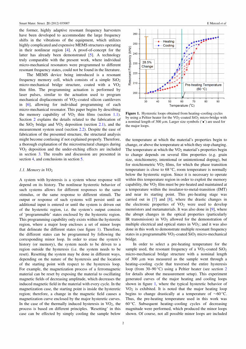
Figure 1. Hysteretic loops obtained from heating–cooling cyclesby using a Peltier heater for the VO2-coated SiO2 micro-bridge witha nominal length of 300 µm. Larger size symbols (‘•’) are used forthe major loops.
the temperature at which the material’s properties begin tochange, or above the temperature at which they stop changing.The temperature at which the VO2 material’s properties beginto change depends on several film properties (e.g. grainsize, stoichiometry, intentional or unintentional doping), butfor stoichiometric VO2 films, for which the phase transitiontemperature is close to 68 ◦C, room temperature is normallybelow the hysteretic region. Since it is necessary to operatewithin this temperature region in order to exploit the memorycapability, the VO2 film must be pre-heated and maintained ata temperature within the insulator-to-metal-transition (IMT)and near its starting point. This pre-heating stage wascarried out in [7] and [8], where the drastic changes inthe electronic properties of VO2 were used to developmemristors and metamaterials. It was also done in [9], wherethe abrupt changes in the optical properties (particularlyIR transmission) in VO2 allowed for the demonstration ofmultiple electrical and optical states in VO2; and it was alsodone in this work to demonstrate multiple resonant frequencystates in a programmable VO2-coated SiO2 micro-mechanicalbridge.
In order to select a pre-heating temperature for thesample used, the resonant frequency of a VO2-coated SiO2micro-mechanical bridge structure with a nominal lengthof 300 µm was measured as the sample went through aheating–cooling cycle that traversed the entire hysteresisloop (from 30–90 ◦C) using a Peltier heater (see section 2for details about the measurement setup). This experimentgenerated curves of the major heating and cooling loopsshown in figure 1, where the typical hysteretic behavior ofVO2 is exhibited. It is noted that the major heating loopbegins to change drastically at a temperature of ∼60 ◦C.Thus, the pre-heating temperature used in this work was60 ◦C. Subsequent heating–cooling cycles of decreasingmagnitude were performed, which produced the minor loopsshown. Of course, not all possible minor loops are included
2

Smart Mater. Struct. 21 (2012) 035007 E Merced et al
in figure 1. The resonant frequency values at a particulartemperature represent only some of the possible resonantfrequency memory states in the VO2-coated SiO2 bridge. Forexample, from figure 1, at 60 ◦C, the range of ‘programmable’resonant frequencies can be seen to be in the approximateregion between 215 and 235 kHz. The exact frequency stateswill be determined by the input sequence, which in this workwas established in the form of increases in temperature causedby laser pulses.
2. Experimental procedures
2.1. SiO2 micro-resonators and VO2 deposition
A 4.15 µm thick SiO2 layer was deposited on standardp-type 4′′ silicon (Si) wafer by using gigascale integrationplasma-enhanced chemical vapor deposition (GSI PECVD)at a temperature of 350 ◦C. The SiO2 was patternedusing reactive ion etching (RIE) and standard lithographytechniques to form a set of micro-bridge structures withlengths from 100 to 500 µm, which shared the same anchor.The Si wafer was then diced to form chips of 7.5 mm2 in area.The SiO2 micro-resonators were released by isotropic etchingof the Si substrate using xenon difluoride (XeF2) gas. Theisotropic etching also removed part of the Si underneath theanchors, creating an undercut effect that changed the effectivelength of the micro-bridges. This undercut was considered inthe subsequent analysis.
A chip containing the released SiO2 micro-bridges wasattached with silver paste to a glass substrate. A 150 nmthick VO2 film was then deposited on the sample (glasssubstrate and chip) by pulsed laser deposition (PLD) in avacuum chamber with a background pressure of 10−6 Torr.During deposition, gas flows of 10 sccm (Ar) and 15 sccm(O2) were independently adjusted using mass flow controllersto result in a chamber pressure of 50 mTorr. Once thedeposition pressure and temperature conditions were met, thesubstrate heater was adjusted to 550 ◦C. Laser ablation ofa vanadium metal target followed, using a krypton fluorideexcimer (λ = 248 nm) laser with fluence 4 J cm−2, pulseduration ∼20 ns, and repetition rate of 10 Hz. After VO2deposition, the chip was detached from the glass substrate,which was then used for XRD analysis and for measuringthe VO2 film thickness by scanning a surface profiler acrossthe VO2 film step created by the removal of the chip.Figure 2 shows the measured resistance of the VO2 filmas a function of temperature—measured from the samesample used for XRD—for a single heating–cooling cycleacross the IMT, which demonstrates that the film coatingthe SiO2 cantilevers is indeed a vanadium oxide film withstoichiometry at least closer to VO2 than to any other form ofvanadium oxide. XRD θ–2θ scans showed only peaks fromthe VO2 film that correspond to reflections from the (011)monoclinic (M1) planes. This showed that, although the filmsare polycrystalline, they are well oriented, with (011)monoclinicplanes parallel to the substrate surface.
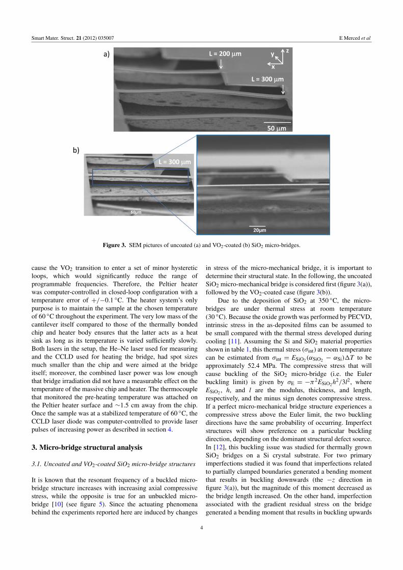
Figure 3(a) shows a SEM image of a released set ofuncoated SiO2 micro-bridges from a chip, which during the
Figure 2. Measured resistance of VO2 film as a function oftemperature across the IMT for a single heating–cooling cycle usinga Peltier heater.
fabrication process was next to SiO2 micro-bridges that werelater coated with VO2. Figure 3(b) shows a SEM image ofthe set of micro-bridges after VO2 deposition, on which theresonant frequency programming measurements were made.Several observations can be made from the figures, the mostobvious being the difference in buckling before and after VO2deposition. This is discussed and explained in section 3.1 ofthis paper.
2.2. Measurement system and procedure
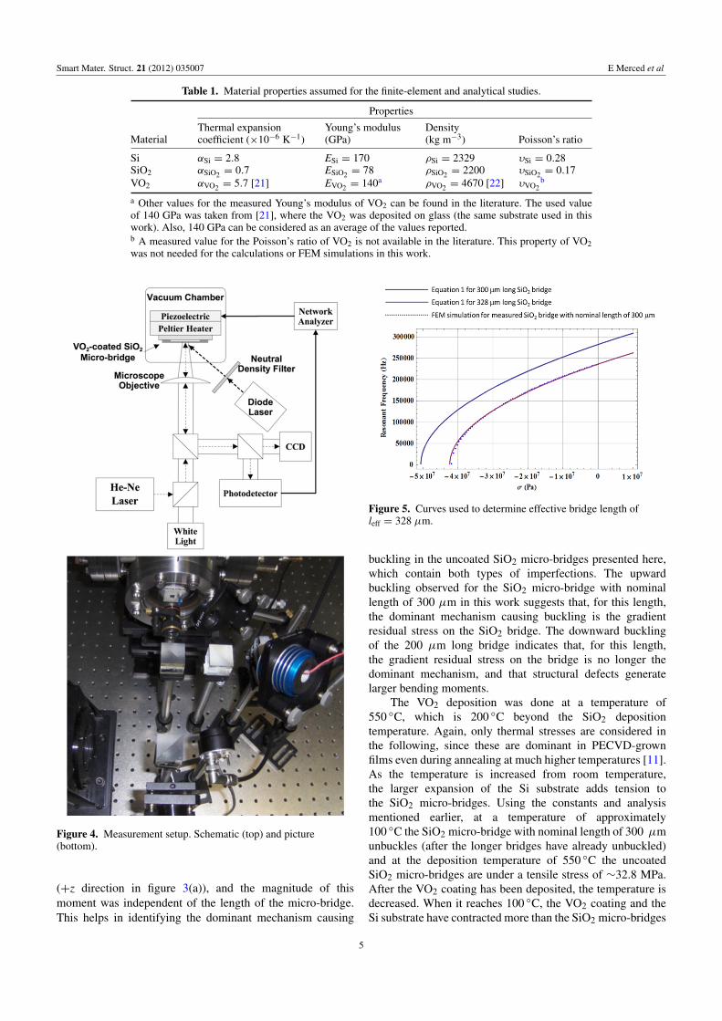
The measurement setup used, shown in figure 4, wasvery similar to the one described elsewhere [5]. Resonantfrequency measurements were conducted in a small chamberwith an optical window, at a pressure below 10 mTorr. A5 mW He–Ne laser was used for measuring the bridge’sresonant frequency, while a current-controlled laser diode(CCLD) (λ= 635 nm, maximum power= 350 mW) was usedto provide the heating light energy pulses that programmed theresonant frequency of the VO2-coated SiO2 micro-mechanicalbridge. It was verified that the optical irradiation from theHe–Ne laser (after the losses caused by the beam splitters,lenses and window) did not cause an increase in temperaturesufficient to influence the phase transition of the VO2 coating.The CCLD laser was focused at the center of the micro-bridgeat an incidence angle of∼45◦ and with a spot size of∼75 µm,which overfilled the bridge. The power output of the CCLDwas calibrated using an optical power meter (Thorlabs modelPM100D) and it was verified to be a linear function of thelaser’s input current. Power losses caused by the glass windowand the neutral density filter were measured and found to bearound 8% and 70%, respectively, for practically the entirepower range, as expected.
The chip was attached to a Peltier heater usingconductive silver paste. For the experiments presented here,it is important to ensure that the temperature increasesmonotonically during the pre-heating process in orderto follow the major heating loop. A small temperatureincrease–decrease sequence in the pre-heating process may
3
Smart Mater. Struct. 21 (2012) 035007 E Merced et al
Figure 3. SEM pictures of uncoated (a) and VO2-coated (b) SiO2 micro-bridges.
cause the VO2 transition to enter a set of minor hystereticloops, which would significantly reduce the range ofprogrammable frequencies. Therefore, the Peltier heaterwas computer-controlled in closed-loop configuration with atemperature error of +/−0.1 ◦C. The heater system’s onlypurpose is to maintain the sample at the chosen temperatureof 60 ◦C throughout the experiment. The very low mass of thecantilever itself compared to those of the thermally bondedchip and heater body ensures that the latter acts as a heatsink as long as its temperature is varied sufficiently slowly.Both lasers in the setup, the He–Ne laser used for measuringand the CCLD used for heating the bridge, had spot sizesmuch smaller than the chip and were aimed at the bridgeitself; moreover, the combined laser power was low enoughthat bridge irradiation did not have a measurable effect on thetemperature of the massive chip and heater. The thermocouplethat monitored the pre-heating temperature was attached onthe Peltier heater surface and ∼1.5 cm away from the chip.Once the sample was at a stabilized temperature of 60 ◦C, theCCLD laser diode was computer-controlled to provide laserpulses of increasing power as described in section 4.
3. Micro-bridge structural analysis
3.1. Uncoated and VO2-coated SiO2 micro-bridge structures
It is known that the resonant frequency of a buckled micro-bridge structure increases with increasing axial compressivestress, while the opposite is true for an unbuckled micro-bridge [10] (see figure 5). Since the actuating phenomenabehind the experiments reported here are induced by changes
in stress of the micro-mechanical bridge, it is important todetermine their structural state. In the following, the uncoatedSiO2 micro-mechanical bridge is considered first (figure 3(a)),followed by the VO2-coated case (figure 3(b)).
Due to the deposition of SiO2 at 350 ◦C, the micro-bridges are under thermal stress at room temperature(30 ◦C). Because the oxide growth was performed by PECVD,intrinsic stress in the as-deposited films can be assumed tobe small compared with the thermal stress developed duringcooling [11]. Assuming the Si and SiO2 material propertiesshown in table 1, this thermal stress (σint) at room temperaturecan be estimated from σint = ESiO2(αSiO2 − αSi)1T to beapproximately 52.4 MPa. The compressive stress that willcause buckling of the SiO2 micro-bridge (i.e. the Eulerbuckling limit) is given by σE = −π
2ESiO2h2/3l2, whereESiO2 , h, and l are the modulus, thickness, and length,respectively, and the minus sign denotes compressive stress.If a perfect micro-mechanical bridge structure experiences acompressive stress above the Euler limit, the two bucklingdirections have the same probability of occurring. Imperfectstructures will show preference on a particular bucklingdirection, depending on the dominant structural defect source.In [12], this buckling issue was studied for thermally grownSiO2 bridges on a Si crystal substrate. For two primaryimperfections studied it was found that imperfections relatedto partially clamped boundaries generated a bending momentthat results in buckling downwards (the −z direction infigure 3(a)), but the magnitude of this moment decreased asthe bridge length increased. On the other hand, imperfectionassociated with the gradient residual stress on the bridgegenerated a bending moment that results in buckling upwards
4
Smart Mater. Struct. 21 (2012) 035007 E Merced et al
Table 1. Material properties assumed for the finite-element and analytical studies.
Material
Properties
Thermal expansioncoefficient (×10−6 K−1)
Young’s modulus(GPa)
Density(kg m−3) Poisson’s ratio
Si αSi = 2.8 ESi = 170 ρSi = 2329 υSi = 0.28SiO2 αSiO2 = 0.7 ESiO2 = 78 ρSiO2 = 2200 υSiO2 = 0.17VO2 αVO2 = 5.7 [21] EVO2 = 140a ρVO2 = 4670 [22] υVO2
b
a Other values for the measured Young’s modulus of VO2 can be found in the literature. The used valueof 140 GPa was taken from [21], where the VO2 was deposited on glass (the same substrate used in thiswork). Also, 140 GPa can be considered as an average of the values reported.b A measured value for the Poisson’s ratio of VO2 is not available in the literature. This property of VO2was not needed for the calculations or FEM simulations in this work.
Figure 4. Measurement setup. Schematic (top) and picture(bottom).
(+z direction in figure 3(a)), and the magnitude of thismoment was independent of the length of the micro-bridge.This helps in identifying the dominant mechanism causing
Figure 5. Curves used to determine effective bridge length ofleff = 328 µm.
buckling in the uncoated SiO2 micro-bridges presented here,which contain both types of imperfections. The upwardbuckling observed for the SiO2 micro-bridge with nominallength of 300 µm in this work suggests that, for this length,the dominant mechanism causing buckling is the gradientresidual stress on the SiO2 bridge. The downward bucklingof the 200 µm long bridge indicates that, for this length,the gradient residual stress on the bridge is no longer thedominant mechanism, and that structural defects generatelarger bending moments.
The VO2 deposition was done at a temperature of550 ◦C, which is 200 ◦C beyond the SiO2 depositiontemperature. Again, only thermal stresses are considered inthe following, since these are dominant in PECVD-grownfilms even during annealing at much higher temperatures [11].As the temperature is increased from room temperature,the larger expansion of the Si substrate adds tension tothe SiO2 micro-bridges. Using the constants and analysismentioned earlier, at a temperature of approximately100 ◦C the SiO2 micro-bridge with nominal length of 300 µmunbuckles (after the longer bridges have already unbuckled)and at the deposition temperature of 550 ◦C the uncoatedSiO2 micro-bridges are under a tensile stress of ∼32.8 MPa.After the VO2 coating has been deposited, the temperature isdecreased. When it reaches 100 ◦C, the VO2 coating and theSi substrate have contracted more than the SiO2 micro-bridges
5

Smart Mater. Struct. 21 (2012) 035007 E Merced et al
(see thermal expansion coefficients in table 1). At this point,the now coated micro-bridges experience a tensile stress dueto the contraction of VO2 (VO2 is still in its tetragonal phaseat this temperature), which is larger in magnitude than thecompressive stress due to the Si contraction. Therefore, ata temperature of 100 ◦C, the VO2-coated micro-bridge isunbuckled and under tensile stress. When the temperatureis further decreased to 30 ◦C, the VO2 thin film transformsfrom its tetragonal phase to its monoclinic phase. Duringthis transition, the volume of the VO2 unit cell crystallitedecreases slightly (actually, due to the lower symmetry ofthe monoclinic lattice in relation to the tetragonal lattice,the conventional unit cell is ‘doubled’ in the monoclinicphase in comparison with the tetragonal lattice [13], so thevolumes to be compared are those of the monoclinic unitcell and twice the volume of the tetragonal unit cell), butthe area of the (011) plane bound by the unit cell—whichis parallel to the surface of SiO2—increases. The expansionof this VO2 plane and the contraction of the Si substrate(which is shrinking at a constant rate) add compression tothe VO2-coated micro-bridge. However, this compression isnot enough to cause buckling of the coated micro-bridgewith a nominal length of 300 µm, which is the one with thelowest σE. From this point on, the discussion is focused onthe VO2-coated SiO2 bridge with nominal length of 300 µmshown in figure 3(b).
After VO2 deposition, the bridge was ready for resonantfrequency measurements as described in section 2, where thedevice temperature is raised to a value such that the VO2 filmmaterial is within the phase transition region (60 ◦C). Just asin [5], the change in stress that caused the resonant frequencyshift in this work was effected by controlling the transition ofthe VO2 coating from its monoclinic phase to its tetragonalphase in the laser-heated bridge. During this transition thecoating (the (011) plane of the VO2 microcrystals) contractsmuch faster than the Si substrate expands; therefore, tensionis added to the micro-bridge during the heating cycle acrossthe IMT of the VO2. Since the VO2-coated micro-bridge isunbuckled at room temperature, this increase in tension isexpected to increase its resonant frequency, as was verifiedexperimentally (see below). It should be noted that in [5],the VO2 was deposited under different conditions, and theVO2-coated micro-bridge was buckled at room temperature.In that case, the resonant frequency decreased with tension.
3.2. Under-etching effects
Previous studies on under-etched resonators(micro-cantilevers) resulting from an isotropic etching releasestep show that the under-etching effect can be taken intoconsideration by changing the length of the cantilever L toan ‘effective length’ L+1L [14]. The resonant frequency fordifferent modes was plotted as a function of 1/ (L+1L)2,and a least-square fit was used to determine 1L. In thework presented in this paper, the value for 1l for the SiO2bridge with a nominal length of 300 µm was obtained fromfinite-element simulations as described below.
Figure 6. Structure drawn in COMSOL Multiphysics. Thedimensions of the drawing were taken from SEM images.Under-etching effects were considered in the finite-element study.
For an unbuckled SiO2 micro-bridge, the first moderesonant frequency (f1u) increases with added tension asdescribed by [10]:
f1u =κ2
1
2π
√ESiO2 I
ρAl4
(1+
γ1σwhl2
12ESiO2 I
)(1)
where κ1 = 4.73, γ1 = 0.2949, w is the bridge’s width(45 µm in the present case), σ is the axial tensile stress,and A = wh and I = wh3/12 are the cross-sectional area andmoment of inertia, respectively. Equation (1) is plotted as afunction of axial stress σ in figure 5 for a 300 µm long SiO2bridge, using the properties in table 1. The entire structurecontaining the uncoated SiO2 micro-bridges was modeledwith the finite-element method simulation software COMSOLMultiphysics (figure 6). The under-etching was includedas measured from SEM images, including the protrusion,following the method described in [14]. Using COMSOL’sSolid Mechanics Module, the resonant frequency of the SiO2bridge with a nominal length of 300 µm was obtained as afunction of applied axial stress using the mechanical SiO2properties shown in table 1 (see figure 5). It was found thata length of l = 328 µm in (1) resulted in a match with thecurve from the simulation.
Therefore, hereafter the effective length of leff = 328 µmis used for the bridge with a nominal length of 300 µm.
For the case of a VO2-coated SiO2 micro-bridge, (1)can be modified by considering the film coating propertiesand dimensions in the ESiO2 I and ρA products, respectively.Effective values were calculated by using [15]:
(EI)eff =w1
12
×E2
1h41 + E2
2h42 + 2E1h1E2h2(2h2
1 + 2h22 + 3h1h2)
E1h1 + E2h2, (2)
(ρA)eff = w1(ρ1h1 + ρ2h2), (3)
where the subscripts ‘1’ and ‘2’ are used to differentiate thefilm coating (VO2) and bridge structure (SiO2) parameters,
6

Smart Mater. Struct. 21 (2012) 035007 E Merced et al
Figure 7. Plot of equation (4) using the parameters shown intable 1. The range of frequencies covered by the major heating andcooling curves shown in figure 1 and by the programming laserpulses are labeled.
respectively. Considering these effective values, the resonantfrequency of an unbuckled VO2-coated micro-bridge can beexpressed as:
fu =
{1.06[E2
1h41 + E2
2h42 + E1E2h1h2(4h2
1 + 4h22 + 6h1h2)]
(ρ1h1 + ρ2h2)(E1h1 + E2h2)l4
+0.311σ(h1 + h2)
(ρ1h1 + ρ2h2)l2
}1/2
. (4)
The EIeff product was used also to calculate an effectiveEuler stress limit (σEeff ) of −46.4 MPa for the 328 µm longVO2-coated SiO2 micro-bridge by using:
σEeff = −πEIeff4
l2w(h1 + h2)= −46.4 MPa. (5)
Equation (4) is plotted in figure 7 as a function of axial stress(σ ) for the unbuckled 328 µm long, 45 µm wide, 4.15 µmthick VO2-coated bridge used for the frequency programmingexperiments. This graph will be used in section 4 toapproximate the change in stress induced by the phase changeof the VO2 thin film.
4. Results and discussion
The measured resonant frequencies in the range oftemperature where the IMT occurs (room temperature to100 ◦C) are much larger for the uncoated buckled SiO2micro-bridge than for its VO2-coated version (440–426 kHzfor the uncoated case, and 200–255 kHz for the VO2-coatedcase). This observation resembles the results in [5], andcan be explained by the difference in the slopes of thecurves for a buckled and unbuckled bridge (see [10, 16,17]). In the present case, based on the trace of (4) infigure 7, the measured room temperature resonant frequencyof 200 kHz for the unbuckled VO2-coated SiO2 micro-bridgecase corresponds to a compressive stress of ∼16.42 MPa(∼30 MPa above the Euler limit), whereas the measuredresonant frequency of 255 kHz at 90 ◦C (after the IMT)corresponds to a tensile stress of∼3.37 MPa (∼50 MPa above
the Euler limit). This indicates that the resonant frequencyincrease of 55 kHz is due to a net 19.79 MPa of addedtensile stress across the IMT, considering the tensile stressadded by the VO2 contraction and Si expansion. This is,of course, assuming that the dominant factor affecting theresonant frequency of the VO2-coated SiO2 micro-bridge isthe stress induced by the contraction of the VO2 thin filmcaused by its phase transformation, rather than the changesin temperature-dependent mechanical properties of the twomaterials composing the micro-bridge. This assumption wasdemonstrated in previous work [5], but for illustrativepurposes, the following explains the case for the VO2-coatedunbuckled SiO2 bridge presented in this paper.
The resonant frequency for a bimorph micro-bridgewith no initial stress is given by the same (4) with σ = 0(i.e. eliminating the second term inside the radical). For theVO2-coated SiO2 micro-bridge presented here, if the changesin stress are neglected, and assuming no initial stress and anincrease in the Young’s modulus of SiO2 of 5% (previousstudies show lower increases [18]), the measured change inresonant frequency across the IMT for this particular bridgeof 28.5% (see figure 1) would have required an increasein the Young’s modulus of VO2 of 600%, which is notrealistic, based on previous studies [19–21]. Assuming aninitial stress different from zero—which is the case presentedhere—would have required an even larger change in theYoung’s modulus of VO2. Therefore, the axial stress isalso the determining parameter in the change in resonantfrequency of the VO2-coated SiO2 micro-bridge tested. Forsimplicity, the mechanical properties (Young’s modulus anddensity) shown in table 1 were assumed to be independent oftemperature when used to generate the plots shown in figures 5and 7.
After the VO2-coated sample was pre-heated to 60 ◦C,localized laser pulses from the CCLD were used to increasethe temperature of individual micro-bridges. In this work,the laser pulses had a duration of 1 ms. From the CCLDcalibration curve, the power of the first laser pulse was1 mW (energy of 1 µJ), which after considering the∼45◦ incident angle, the bridge width, and the laser spotsize, was approximated to 0.7 mW (energy of 0.7 µJ)delivered to the micro-bridges. The energy of subsequentlaser pulses increased in steps of 0.7 µJ, with the last laserpulse delivering 9.1 µJ (13 pulses in total). Figure 8 showsthe resonant frequency peaks measured after each pulse.Energy steps of equal magnitude would have bounded theresonant frequency states to values between the resonantfrequency at the pre-heating temperature and the resonantfrequency after the first laser pulse—significantly limitingthe range of programmable frequencies. On the other hand,although subsequent pulses with increasing energies wouldyield a broader range of programmable frequencies (due to thelarger heating excursions), they would have allowed a smallernumber of possible resonant frequency states. An explanationfor this statement follows.
The magnitude of the resonant frequency change dueto a laser pulse will depend on the energy delivered by thelaser pulse and on the location inside the hysteretic region
7

Smart Mater. Struct. 21 (2012) 035007 E Merced et al
Figure 8. Resonant frequency peaks for every heating laser pulse.Different resonant curve widths may be due to the energydissipation mechanisms induced by the structural changes of theVO2 material during the phase change, or by the heat absorbed tocause the transition itself (i.e. latent heat).
of the resonant frequency state before the laser pulse isapplied. Larger intensities and/or durations will result in moreenergy being delivered to the VO2 film and larger increasesin temperature, causing larger resonant frequency changes.In a separate experiment, it was observed that, startingat the pre-heating temperature, a single pulse delivering2.8 µJ caused practically the same change in resonantfrequency as four individual pulses delivering 0.7, 1.4, 2.1,and 2.8 µJ, respectively. Therefore, larger magnitudes ofincreasing energy steps result in lower possible frequencystates. This effect has been observed before in the fully optical(optical reading and writing) memory states in VO2 [9].
The energy absorbed from the first laser pulse transientlyincreases the temperature of the VO2 thin film, causing achange in resonant frequency that is expected to follow themajor heating loop shown in figure 1. After the initial laserpulse, the sample returns to the pre-heating temperature of60 ◦C following one of the minor cooling loops—becauseof the hysteresis, however, the bridge resonant frequencydoes not return to the same value as before the laser pulse.Subsequent laser pulses will increase the temperature again,but each time the resonant frequency change will followa different minor heating and cooling loop, respectively,during and after each pulse. In the present case, it is notpossible to actually measure the excursion of the resonantfrequency after each laser pulse, since this would requirereal-time measurements of the resonant frequency during thelaser pulses and during the decrease in temperature to 60 ◦C,which are processes lasting at most a few milliseconds—asingle frequency sweep of the network analyzer takes ∼30 s.Figure 9 shows the resonant frequency states and the datafor the major heating loop (shown completely in figure 1)corresponding to the temperature range of 60–64 ◦C. Sincethe minor loops that produced these frequency states cannot beobtained experimentally, it is not possible to match every laser
Figure 9. Resonant frequency states and part of the major heatingloop shown in figure 1.
Figure 10. Programmed resonant frequency states for every pulse.Only a few incremental energies have been marked for clarity.
pulse with a precise increase in temperature. However, thedecrease in the change of resonant frequency with increasingenergy pulses (see also figure 10) indicates that the minorcooling curves get closer to each other with intermittentincreases in temperature of increasing magnitude. Practically,the heating pulse-induced resonant frequency changes ofthe VO2-coated micro-bridge saturate as a frequency of∼222.7 kHz is approached. From figure 1, it can be noticedthat this saturation frequency of 222.7 kHz is below thehighest frequency value possible at 60 ◦C of 235 kHz, whichis the frequency value in the major cooling loop at 60 ◦C.
Therefore, there is a trade-off between the range of pro-grammable frequencies and the number of programmable fre-quency states. Since the magnitude of the increasing steps isdiscretionary, the magnitude of the increasing energy steps of
8

Smart Mater. Struct. 21 (2012) 035007 E Merced et al
0.7 µJ was considered to be a convenient value to demonstratethe resonant frequency memory states in this work. The laserpulses were triggered every 2 min, which allowed enough timeto measuring the resonant frequency after each pulse. It wasobserved that after each pulse, the resonant frequency of themicro-mechanical bridge did not change notably until the nextpulse was triggered. Furthermore, in a separate experiment, itwas observed that the frequency ‘state’ of the micro-bridgecould remain essentially unchanged for more than 24 h, witha shift of only 80 Hz (better than 0.04%), as long as the heatermaintained the device at a constant temperature of 60 ◦C.
The programming of frequency states reported in thispaper was found to be repeatable after ‘resetting’ the memoryof the VO2 thin film.
5. Conclusion
A MEMS-based multiple state mechanical resonant frequencymemory has been demonstrated. The resonant frequencystates have been programmed with the use of laser pulsesfrom a CCLD. The programmable states are located at thepre-heating temperature resonant frequency values of minorcooling curves, and were found to remain for more than24 h, as long as the sample is kept at the pre-heatingtemperature of 60 ◦C. The stress levels experienced by themicro-bridge (before and after VO2 deposition) have beendescribed. One question that remains to be answered andis the subject of ongoing research is the effect of the VO2thin film thickness on the induced stress in the mechanicalstructure. The presented device represents the cell of amicro-mechanical-based frequency memory array.
Acknowledgments
This work was supported by the National Science Foundationunder grants no. ECCS-0954406 (CAREER Program), andno. DGE-0802267 (GRFP Program).
References
[1] van Bladel J 1953 A controlled-frequency oscillator withfrequency ‘memory’ J. Sci. Instrum. 30 299–301
[2] Tucker R S and Riding J L 2009 Optical ring-resonatorrandom-access memory J. Lightwave Technol. 26 320–8
[3] Hoppensteadt F C and Izhikevich E M 2001 Synchronizationof MEMS resonators and mechanical neurocomputingIEEE Trans. Circuits Syst. 48 133–8
[4] Marzencki M, Defosseux M and Basrour S 2009 MEMSvibration energy harvesting devices with passive resonancefrequency adaptation capability J. Microelectromech. Syst.18 1444–53
[5] Merced E, Cabrera R, Coy H, Fernandez F E andSepulveda N 2011 Frequency tuning of VO2-coatedbuckled microbridges J. Microelectromech. Syst. 20 558–60
[6] Cabrera R, Merced E, Davila N, Fernandez F E andSepulveda N 2011 A multiple-state micro-mechanicalprogrammable memory J. Microelectron. Eng. 88 3231–4
[7] Driscoll T, Kim H-T, Chae B-G, Di Ventra M andBasov D N 2009 Phase-transition driven memristive systemAppl. Phys. Lett. 95 043503
[8] Driscoll T, Kim H-T, Chae B-G, Kim B-J, Lee Y-W,Marie Jokerst N, Palit S, Smith D R, Di Ventra M andBasov D N 2009 Memory metamaterials Science325 1518–21
[9] Coy H, Cabrera R, Sepulveda N and Fernandez F E 2010Opto-electronic and full-optical multiple state memoryresponse in phase-change materials J. Appl. Phys.108 113115
[10] Bouwstra S and Geijselaers B 1991 On the resonancefrequencies of microbridges Proc. IEEE Transducerspp 538–42
[11] Bhushan B, Muraka S P and Gerlach J 1990 Stress in silicondioxide films deposited using chemical vapor depositiontechniques and the effect of annealing on these stressesJ. Vac. Sci. Technol. B 8 1068–74
[12] Fang W, Lee C-H and Hu H-H 1999 On the buckling behaviorof micromachined beams J. Micromech. Microeng.9 236–44
[13] Powder Diffraction Files nos. 82–0661 and 79–1655International Centre for Diffraction Data, Pennsylvania
[14] Babaei Gavan K, van der Drift E W J M, Venstra W J,Zuiddam M R and van der Zant H S J 2009 Effect ofundercut on the resonant behavior of silicon nitridecantilevers J. Micromech. Microeng. 19 035003
[15] Zhang G, Chu V and Conde J P 2007 Electrostaticallyactuated bilayer polyimide-based microresonatorsJ. Micromech. Microeng. 17 797–803
[16] Kim C S and Dickinson S M 1968 The flexural vibration ofslightly curved slender beams subject to axial enddisplacement J. Sound Vib. 104 170–5
[17] Southworth D R, Bellan L M, Linzon Y, Craighead H G andParpia J M 2010 Stress-based vapor sensing using resonantmicrobridges Appl. Phys. Lett. 96 163503
[18] Spinner S and Cleek G W 1960 Temperature dependence ofYoung’s modulus of vitreous germania and silica J. Appl.Phys. 31 1407–10
[19] Rua A, Fernandez F E, Hines M A and Sepulveda N 2010Study of the resonant frequencies of siliconmicrocantilevers coated with vanadium dioxide films duringthe insulator-to-metal transition J. Appl. Phys. 107 053528
[20] Sepulveda N, Rua A, Cabrera R and Fernandez F 2008Young’s modulus of VO2 thin films as a function oftemperature including insulator-to-metal transition regimeAppl. Phys. Lett. 92 191913
[21] Tsai K-Y, Chin T-S and Shieh H-P D 2004 Effect of graincurvature on nano-indentation measurements of thin filmsJapan. J. Appl. Phys. 43 6268–73
[22] Jin P, Nakao S, Tanemura S, Bell T, Wielunski L S andSwain M V 1999 Characterization of mechanical propertiesof VO2 thin films on sapphire and silicon byultra-microindentation Thin Solid Films 343 134–7
9