lvds frequency-programmable idt8n4s270 crystal oscillator
TRANSCRIPT
DATASHEET
IDT8N4S270CCD REVISION A AUGUST 31, 2012 1 ©2012 Integrated Device Technology, Inc.
LVDS Frequency-Programmable Crystal Oscillator
IDT8N4S270
General Description
The IDT8N4S270 is a Factory Frequency-Programmable Crystal Oscillator with very flexible frequency programming capabilities. The device uses IDT’s fourth generation FemtoClock® NG technology for an optimum of high clock frequency and low phase noise performance. The device accepts 2.5V or 3.3V supply and is packaged in a small, lead-free (RoHS 6) 6-lead ceramic 5mm x 7mm x 1.55mm package.
The device can be factory programmed to any in the range from 15.476MHz to 866.67MHz and from 975MHz to 1,300MHz and supports a very high degree of frequency precision of 218Hz or better. The extended temperature range supports wireless infrastructure, telecommunication and networking end equipment requirements.
Features
• Fourth generation FemtoClock® NG technology
• Factory-programmable clock output frequency from 15.476MHz to 866.67MHz and from 975MHz to 1,300MHz
• Frequency programming resolution is 218Hz and better
• One 2.5V, 3.3V LVDS clock output
• Output enable control (positive polarity), LVCMOS/LVTTLcompatible
• RMS phase jitter @ 231.25MHz (12kHz - 20MHz): 0.48ps (typical), integer PLL feedback configuration
• RMS phase jitter @ 231.25MHz (1kHz - 40MHz): 0.50ps (typical), integer PLL feedback configuration
• 2.5V or 3.3V supply
• -40°C to 85°C ambient operating temperature
• Available in a lead-free (RoHS 6) 6-pin ceramic package
IDT8N4S2706-lead ceramic 5mm x 7mm x 1.55mm
package bodyCD Package
Top View
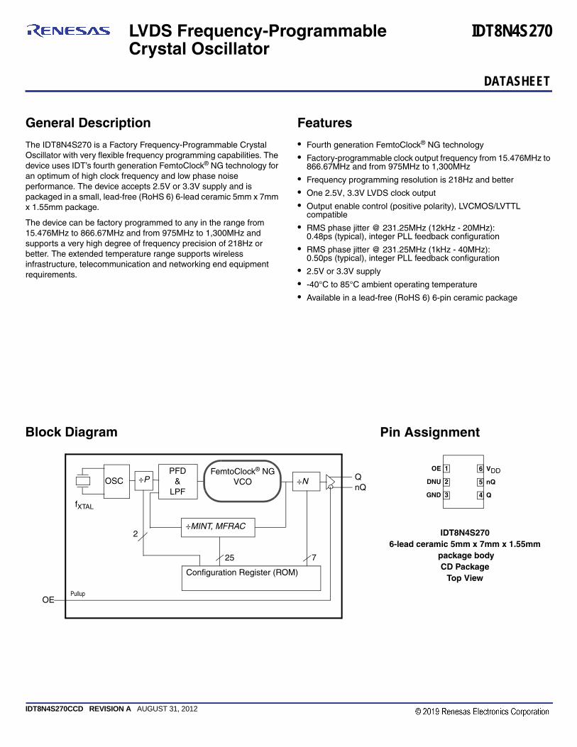
Pin AssignmentBlock Diagram
QnQ
OSC
fXTAL
÷MINT, MFRAC
PFD&
LPF
FemtoClock® NGVCO ÷N
Configuration Register (ROM)
25 7
OEPullup
2
÷P6 VDD
5 nQ
4 Q
OE 1
DNU 2
GND 3

IDT8N4S270 Data Sheet LVDS FREQUENCY-PROGRAMMABLE CRYSTAL OSCILLATOR
IDT8N4S270CCD REVISION A AUGUST 31, 2012 2 ©2012 Integrated Device Technology, Inc.
Pin Description and Characteristic Tables
NOTE: Pullup refers to an internal input resistor. See Table 2, Pin Characteristics, for typical values.
Function Table
Table 3A. OE Configuration
Output EnableOE
0 Outputs Q, nQ are in high-impedance state
1 (default) Outputs Q, nQ are enabled
s
NOTE: OE is an asynchronous control.
Table 1. Pin Descriptions
Number Name Type Description
1 OE Input Pullup Output enable pin. See Table 3A for function. LVCMOS/LVTTL interface levels.
2 DNU Do not use (factory use only).
3 GND Power Power supply ground.
4, 5 Q, nQ Output Differential clock output pair. LVDS interface levels.
6 VDD Power Power supply pin.
Table 2. Pin Characteristics
Symbol Parameter Test Conditions Minimum Typical Maximum Units
CIN Input Capacitance 5.5 pF
RPULLUP Input Pullup Resistor 50 k
Input
IDT8N4S270 Data Sheet LVDS FREQUENCY-PROGRAMMABLE CRYSTAL OSCILLATOR
IDT8N4S270CCD REVISION A AUGUST 31, 2012 3 ©2012 Integrated Device Technology, Inc.
Principles of OperationThe block diagram consists of the internal 3rd overtone crystal and oscillator which provide the reference clock fXTAL of either
114.285MHz or 100MHz. The PLL includes the FemtoClock NG VCO along with the Pre-divider (P), the feedback divider (M) and the post divider (N). The P, M, and N dividers determine the output fre-quency based on the fXTAL reference. The feedback divider is frac-
tional supporting a huge number of output frequencies. The configuration of the feedback divider to integer-only values results in an improved output phase noise characteristics at the expense of the range of output frequencies. Internal registers are used to hold one factory pre-set P, M, and N configuration setting. The P, M, and N frequency configuration supports an output frequency range from 15.476MHz to 866.67MHz and from 975MHz to 1,300MHz.
The devices use the fractional feedback divider with a delta-sigma modulator for noise shaping and robust frequency synthesis capability. The relatively high reference frequency minimizes phase noise generated by frequency multiplication and allows more efficient shaping of noise by the delta-sigma modulator.
The output frequency is determined by the 2-bit pre-divider (P), the feedback divider (M) and the 7-bit post divider (N). The feedback divider (M) consists of both a 7-bit integer portion (MINT) and an 18-bit fractional portion (MFRAC) and provides the means forhigh-resolution frequency generation. The output frequency fOUT is calculated by:
fOUT fXTAL1
P N------------ MINT
MFRAC 0.5+
218
-------------------------------------+ =
Frequency Configuration
An order code is assigned to each frequency configuration programmed by the factory (default frequencies). For more information on the available default frequencies and order codes, please see the Ordering Information section in this document. For available order codes, see the FemtoClock NG Ceramic-Package XO and VCXO Ordering Product Information document.
For more information on programming capabilities of the device for custom frequency and pull-range configurations, see the FemtoClock NG Ceramic 5x7 Module Programming Guide.
.
Table 3B. Output Frequency Range1
15.476MHz to 866.67MHz
975MHz to 1,300MHz
1. Supported output frequency range. The output frequency canbe programmed to any frequency in this range and to a precision of218Hz or better.

IDT8N4S270 Data Sheet LVDS FREQUENCY-PROGRAMMABLE CRYSTAL OSCILLATOR
IDT8N4S270CCD REVISION A AUGUST 31, 2012 4 ©2012 Integrated Device Technology, Inc.
Absolute Maximum RatingsNOTE: Stresses beyond those listed under Absolute Maximum Ratings may cause permanent damage to the device. These ratings are stress specifications only. Functional operation of product at these conditions or any conditions beyond those listed in the DC
Characteristics or AC Characteristics is not implied. Exposure to absolute maximum rating conditions for extended periods may affect product reliability.
Supply Voltage, VDD 3.63V
Inputs, VI -0.5V to VDD + 0.5V
Outputs, IO (LVDS)Continuous CurrentSurge Current
10mA15mA
Package Thermal Impedance, JA 49.4C/W (0 mps)
Storage Temperature, TSTG -65C to 150C
DC Electrical CharacteristicsTable 4A. Power Supply DC Characteristics, VDD = 3.3V ± 5%, TA = -40°C to 85°C
Table 4B. Power Supply DC Characteristics, VDD = 2.5V ± 5%, TA = -40°C to 85°C
Table 4C. LVCMOS/LVTTL DC Characteristic, VDD = 3.3V ± 5% or 2.5V ± 5%, TA = -40°C to 85°C
Item Rating
Symbol Parameter Test Conditions Minimum Typical Maximum Units
VDD Power Supply Voltage 3.135 3.3 3.465 V
IDD Power Supply Current 134 160 mA
Symbol Parameter Test Conditions Minimum Typical Maximum Units
VDD Power Supply Voltage 2.375 2.5 2.625 V
IDD Power Supply Current 129 155 mA
Symbol Parameter Test Conditions Minimum Typical Maximum Units
VIH Input High Voltage OEVDD = 3.3V 2 VDD + 0.3 V
VDD = 2.5V 1.7 VDD + 0.3 V
VIL Input Low Voltage OEVDD = 3.3V -0.3 0.8 V
VDD = 2.5V -0.3 0.7 V
IIH Input High Current OE VDD = VIN = 3.465V or 2.625V 10 µA
IIL Input Low Current OE VDD = 3.465V or 2.625V, VIN = 0V -150 µA

IDT8N4S270 Data Sheet LVDS FREQUENCY-PROGRAMMABLE CRYSTAL OSCILLATOR
IDT8N4S270CCD REVISION A AUGUST 31, 2012 5 ©2012 Integrated Device Technology, Inc.
Table 4D. LVDS DC Characteristics, VDD = 3.3V ± 5%, TA = -40°C to 85°C
Table 4E. LVDS DC Characteristics, VDD = 2.5V ± 5%, TA = -40°C to 85°C
Symbol Parameter Test Conditions Minimum Typical Maximum Units
VOD Differential Output Voltage 247 370 454 mV
VOD VOD Magnitude Change 50 mV
VOS Offset Voltage 1.125 1.22 1.375 V
VOS VOS Magnitude Change 50 mV
Symbol Parameter Test Conditions Minimum Typical Maximum Units
VOD Differential Output Voltage 247 360 454 mV
VOD VOD Magnitude Change 50 mV
VOS Offset Voltage 1.125 1.21 1.375 V
VOS VOS Magnitude Change 50 mV
IDT8N4S270 Data Sheet LVDS FREQUENCY-PROGRAMMABLE CRYSTAL OSCILLATOR
IDT8N4S270CCD REVISION A AUGUST 31, 2012 6 ©2012 Integrated Device Technology, Inc.
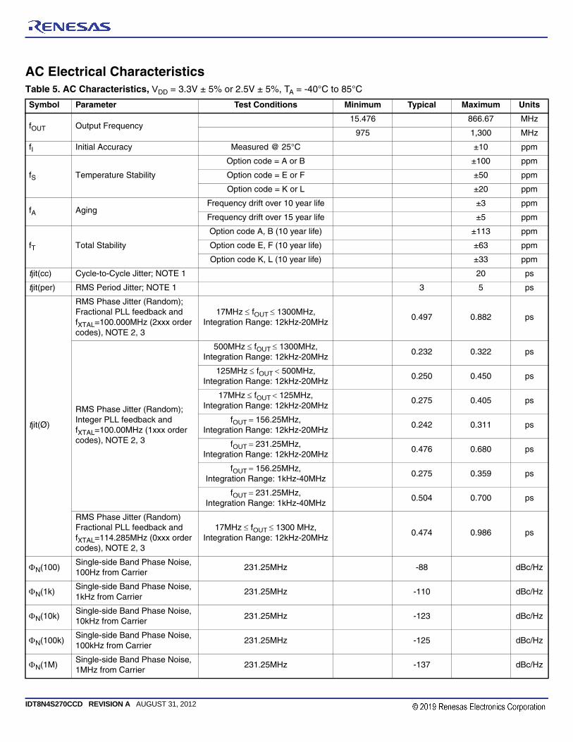
AC Electrical CharacteristicsTable 5. AC Characteristics, VDD = 3.3V ± 5% or 2.5V ± 5%, TA = -40°C to 85°C
Symbol Parameter Test Conditions Minimum Typical Maximum Units
fOUT Output Frequency15.476 866.67 MHz
975 1,300 MHz
fI Initial Accuracy Measured @ 25°C ±10 ppm
fS Temperature Stability
Option code = A or B ±100 ppm
Option code = E or F ±50 ppm
Option code = K or L ±20 ppm
fA AgingFrequency drift over 10 year life ±3 ppm
Frequency drift over 15 year life ±5 ppm
fT Total Stability
Option code A, B (10 year life) ±113 ppm
Option code E, F (10 year life) ±63 ppm
Option code K, L (10 year life) ±33 ppm
tjit(cc) Cycle-to-Cycle Jitter; NOTE 1 20 ps
tjit(per) RMS Period Jitter; NOTE 1 3 5 ps
tjit(Ø)
RMS Phase Jitter (Random);Fractional PLL feedback andfXTAL=100.000MHz (2xxx order codes), NOTE 2, 3
17MHz fOUT 1300MHz,Integration Range: 12kHz-20MHz
0.497 0.882 ps
RMS Phase Jitter (Random);Integer PLL feedback andfXTAL=100.00MHz (1xxx order codes), NOTE 2, 3
500MHz fOUT 1300MHz,Integration Range: 12kHz-20MHz
0.232 0.322 ps
125MHz fOUT 500MHz,Integration Range: 12kHz-20MHz
0.250 0.450 ps
17MHz fOUT 125MHz,Integration Range: 12kHz-20MHz
0.275 0.405 ps
fOUT 156.25MHz,Integration Range: 12kHz-20MHz
0.242 0.311 ps
fOUT 231.25MHz,Integration Range: 12kHz-20MHz
0.476 0.680 ps
fOUT 156.25MHz,Integration Range: 1kHz-40MHz
0.275 0.359 ps
fOUT 231.25MHz,Integration Range: 1kHz-40MHz
0.504 0.700 ps
RMS Phase Jitter (Random)Fractional PLL feedback andfXTAL=114.285MHz (0xxx order codes), NOTE 2, 3
17MHz fOUT 1300 MHz,Integration Range: 12kHz-20MHz
0.474 0.986 ps
N(100)Single-side Band Phase Noise, 100Hz from Carrier
231.25MHz -88 dBc/Hz
N(1k)Single-side Band Phase Noise, 1kHz from Carrier
231.25MHz -110 dBc/Hz
N(10k)Single-side Band Phase Noise, 10kHz from Carrier
231.25MHz -123 dBc/Hz
N(100k)Single-side Band Phase Noise, 100kHz from Carrier
231.25MHz -125 dBc/Hz
N(1M)Single-side Band Phase Noise, 1MHz from Carrier
231.25MHz -137 dBc/Hz

IDT8N4S270 Data Sheet LVDS FREQUENCY-PROGRAMMABLE CRYSTAL OSCILLATOR
IDT8N4S270CCD REVISION A AUGUST 31, 2012 7 ©2012 Integrated Device Technology, Inc.
NOTE: Electrical parameters are guaranteed over the specified ambient operating temperature range, which is established when the device is mounted in a test socket with maintained transverse airflow greater than 500lfpm. The device will meet specifications after thermal equilibrium has been reached under these conditions.NOTE: XTAL parameters (initial accuracy, temperature stability, aging and total stability) are guaranteed by manufacturing.NOTE 1: This parameter is defined in accordance with JEDEC standard 65.NOTE 2: Please refer to the phase noise plot.NOTE 3: Please see the FemtoClock NG Ceramic 5x7 Modules Programming guide for more information on PLL feedback modes and the optimum configuration for phase noise. Integer PLL feedback is the default operation for the dddd = 1xxx order codes.
N(10M)Single-side band phase noise, 10MHz from Carrier
231.25MHz -141 dBc/Hz
tR / tF Output Rise/Fall Time 20% to 80% 50 450 ps
odc Output Duty Cycle 47 53 %
tSTARTUPDevice Startup Time After Power Up
20 ms
Table 5. AC Characteristics, VDD = 3.3V ± 5% or 2.5V ± 5%, TA = -40°C to 85°C
Symbol Parameter Test Conditions Minimum Typical Maximum Units

IDT8N4S270 Data Sheet LVDS FREQUENCY-PROGRAMMABLE CRYSTAL OSCILLATOR
IDT8N4S270CCD REVISION A AUGUST 31, 2012 8 ©2012 Integrated Device Technology, Inc.
Typical Phase Noise at 231.25MHz (12kHz - 20MHz)
Noi
se P
ower
dBc
Hz
Offset Frequency (Hz)

IDT8N4S270 Data Sheet LVDS FREQUENCY-PROGRAMMABLE CRYSTAL OSCILLATOR
IDT8N4S270CCD REVISION A AUGUST 31, 2012 9 ©2012 Integrated Device Technology, Inc.
Parameter Measurement Information
2.5V LVDS Output Load AC Test Circuit
RMS Phase Jitter
Cycle-to-Cycle Jitter
3.3V LVDS Output Load AC Test Circuit
RMS Period Jitter
Output Duty Cycle/Pulse Width/Period
SCOPEQ
nQ
2.5V±5% POWER SUPPLY+ –Float GND
VDD
Offset Frequencyf1 f2
Phase Noise Plot
Area Under Curve Defined by the Offset Frequency Markers
RMS Phase Jitter =
Noi
se P
ower
2 * * ƒ1
*
nQ
Q
➤
➤
➤
➤
tcycle n tcycle n+1
tjit(cc) = |tcycle n – tcycle n+1|1000 Cycles
SCOPEQ
nQ
3.3V±5% POWER SUPPLY+ –Float GND
VDD
VOH
VREF
VOL
Mean Period(First edge after trigger)
Reference Point(Trigger Edge)
1σ contains 68.26% of all measurements2σ contains 95.4% of all measurements3σ contains 99.73% of all measurements4σ contains 99.99366% of all measurements6σ contains (100-1.973x10⁻⁷)% of all measurements
Histogram
tPW
tPERIOD
tPW
tPERIOD
odc = x 100%
nQ
Q

IDT8N4S270 Data Sheet LVDS FREQUENCY-PROGRAMMABLE CRYSTAL OSCILLATOR
IDT8N4S270CCD REVISION A AUGUST 31, 2012 10 ©2012 Integrated Device Technology, Inc.
Parameter Measurement Information, continued
Output Rise/Fall Time
Differential Output Voltage Setup
Offset Voltage Setup
20%
80% 80%
20%
tR tF
VOD
nQ
Q
100
out
out
DC Input
VDD
LVDS
out
out
LVDSDC Input
ä
VOS/Δ VOS
VDD

IDT8N4S270 Data Sheet LVDS FREQUENCY-PROGRAMMABLE CRYSTAL OSCILLATOR
IDT8N4S270CCD REVISION A AUGUST 31, 2012 11 ©2012 Integrated Device Technology, Inc.
Applications Information
LVDS Driver Termination
For a general LVDS interface, the recommended value for the termination impedance (ZT) is between 90 and 132. The actual value should be selected to match the differential impedance (Z0) of your transmission line. A typical point-to-point LVDS design uses a 100 parallel resistor at the receiver and a 100 differential transmission-line environment. In order to avoid any transmission-line reflection issues, the components should be surface mounted and must be placed as close to the receiver as possible. IDT offers a full line of LVDS compliant devices with two types of output structures: current source and voltage source. The
standard termination schematic as shown in Figure 1A can be used with either type of output structure. Figure 1B, which can also be used with both output types, is an optional termination with center tap capacitance to help filter common mode noise. The capacitor value should be approximately 50pF. If using a non-standard termination, it is recommended to contact IDT and confirm if the output structure is current source or voltage source type. In addition, since these outputs are LVDS compatible, the input receiver’s amplitude and common-mode input range should be verified for compatibility with the output.
LVDSDriver
LVDSDriver
LVDSReceiver
LVDSReceiverZT
C
ZO ZT
ZO ZT
ZT2
ZT2
Figure 1A. Standard Termination
Figure 1B. Optional Termination

IDT8N4S270 Data Sheet LVDS FREQUENCY-PROGRAMMABLE CRYSTAL OSCILLATOR
IDT8N4S270CCD REVISION A AUGUST 31, 2012 12 ©2012 Integrated Device Technology, Inc.
Schematic LayoutFigure 2 shows an example IDT8N4S270 application schematic. The schematic example focuses on functional connections and is intended as an example only and may not represent the exact user configuration. Refer to the pin description and functional tables in the datasheet to ensure the logic control inputs are properly set. For example OE and FSEL can be configured from an FPGA instead of set with pull up and pull down resistors as shown.
As with any high speed analog circuitry, the power supply pins are vulnerable to random noise, so to achieve optimum jitter performance isolation of the VDD pin from power supply is required. In order to achieve the best possible filtering, it is recommended that the placement of the filter components be on the device side of the PCB as close to the power pins as possible. If space is limited, the 0.1µF
capacitor on the VDD pin must be placed on the device side with direct return to the ground plane though vias. The remaining filter components can be on the opposite side of the PCB.
Power supply filter component recommendations are a general guideline to be used for reducing external noise from coupling into the devices. The filter performance is designed for a wide range of noise frequencies. This low-pass filter starts to attenuate noise at approximately 10kHz. If a specific frequency noise component is known, such as switching power supplies frequencies, it is recommended that component values be adjusted and if required, additional filtering be added. Additionally, good general design practices for power plane voltage stability suggests adding bulk capacitance in the local area of all devices.
3.3V
C50.1uF
C410uF
VDD
Place 0.1uF bypass capdirectly adjacent tothe VDD pin.
FB1
BLM18BB221SN1
12
C30.1uF
RU2Not Install
VDD VDD
RU11K
RD21K
RD1Not Install
To LogicInputpins
Logic Control Input Examples
Set LogicInput to '1'
Set LogicInput to '0'
To LogicInputpins
OE
LVDS Receiv er
+
-
Zo = 50 Ohm
Zo = 50 Ohm
R1100
U1
OE1
DNU2
GND3
Q4
nQ5
VDD6
Figure 2. IDT8N4S270 Schematic Example

IDT8N4S270 Data Sheet LVDS FREQUENCY-PROGRAMMABLE CRYSTAL OSCILLATOR
IDT8N4S270CCD REVISION A AUGUST 31, 2012 13 ©2012 Integrated Device Technology, Inc.
Power ConsiderationsThis section provides information on power dissipation and junction temperature for the IDT8N4S270. Equations and example calculations are also provided.
1. Power Dissipation.
The total power dissipation for the IDT8N4S270 is the sum of the core power plus the power dissipated due to the load. The following is the power dissipation for VDD = 3.3V + 5% = 3.465V, which gives worst case results.
• Power (core)MAX = VDD_MAX * IDD_MAX = 3.465V * 160mA = 554.4mW
2. Junction Temperature.
Junction temperature, Tj, is the temperature at the junction of the bond wire and bond pad directly affects the reliability of the device. The maximum recommended junction temperature is 125°C. Limiting the internal transistor junction temperature, Tj, to 125°C ensures that the bond wire and bond pad temperature remains below 125°C.
The equation for Tj is as follows: Tj = JA * Pd_total + TA
Tj = Junction Temperature
JA = Junction-to-Ambient Thermal Resistance
Pd_total = Total Device Power Dissipation (example calculation is in section 1 above)
TA = Ambient Temperature
In order to calculate junction temperature, the appropriate junction-to-ambient thermal resistance JA must be used. Assuming no air flow and a multi-layer board, the appropriate value is 49.4°C/W per Table 6 below.
Therefore, Tj for an ambient temperature of 85°C with all outputs switching is:
85°C + 0.554W * 49.4°C/W = 112.4°C. This is below the limit of 125°C.
This calculation is only an example. Tj will obviously vary depending on the number of loaded outputs, supply voltage, air flow and the type of board (multi-layer).
Table 6. Thermal Resistance JA for 6 Lead Ceramic 5mm x 7mm Package, Forced Convection
JA by Velocity
Meters per Second 0 1 2
Multi-Layer PCB, JEDEC Standard Test Boards 49.4°C/W 44.2°C/W 42.1°C/W

IDT8N4S270 Data Sheet LVDS FREQUENCY-PROGRAMMABLE CRYSTAL OSCILLATOR
IDT8N4S270CCD REVISION A AUGUST 31, 2012 14 ©2012 Integrated Device Technology, Inc.
Reliability InformationTable 7. JA vs. Air Flow Table for a 6-lead Ceramic 5mm x 7mm Package
Transistor CountThe transistor count for IDT8N4S270 is: 47,511
JA vs. Air Flow
Meters per Second 0 1 2
Multi-Layer PCB, JEDEC Standard Test Boards 49.4°C/W 44.2°C/W 42.1°C/W

IDT8N4S270 Data Sheet LVDS FREQUENCY-PROGRAMMABLE CRYSTAL OSCILLATOR
IDT8N4S270CCD REVISION A AUGUST 31, 2012 15 ©2012 Integrated Device Technology, Inc.
Package Outline and Package Dimensions

IDT8N4S270 Data Sheet LVDS FREQUENCY-PROGRAMMABLE CRYSTAL OSCILLATOR
IDT8N4S270CCD REVISION A AUGUST 31, 2012 16 ©2012 Integrated Device Technology, Inc.
Ordering Information for FemtoClock NG Ceramic-Package XO and VCXO ProductsThe programmable VCXO and XO devices support a variety of device options such as the output type, number of default frequen- cies, internal crystal frequency, power supply voltage, ambient temperature range and the frequency accuracy. The device options, default frequencies and default VCXO pull range must be specified at the time of order and are programmed by IDT before the shipment. The table below specifies the available order codes, including the device options and default frequency configurations. Example part number: the order code 8N3QV01FG-0001CDI specifies a programmable, quad default-frequency VCXO with a voltage supply of 2.5V, a LVPECL output, a 50ppm crystal frequency accuracy,
contains a 114.285MHz internal crystal as frequency source, industrial temperature range, a lead-free (6/6 RoHS) 6-lead ceramic 5mm x 7mm x 1.55mm package and is factory-programmed to the default frequencies of 100MHz, 122.88MHz, 125MHz and 156.25MHz and to the VCXO pull range of minimum 100ppm.
Other default frequencies and order codes are available from IDT on request. For more information on available default frequencies, see the FemtoClock NG Ceramic-Package XO and VCXO Ordering Product Information document.
Shipping Package8: Tape & Reel(no letter): Tray
Ambient Temperature Range“I”: Industrial: (TA = -40°C to 85°C)(no letter) : (TA = 0°C to 70°C)
Package CodeCD: Lead-Free, 6/10-lead ceramic 5mm x 7mm x 1.55mm
Die RevisionC
Option Code (Supply Voltage and Frequency-Stability)A: VDD = 3.3V±5%, ±100ppmB: VDD = 2.5V±5%, ±100ppmE: VDD = 3.3V±5%, ±50ppmF: VDD = 2.5V±5%, ±50ppmK: VDD = 3.3V±5%, ±20ppmL: VDD = 2.5V±5%, ±20ppm
Default-Frequency and VCXO Pull RangeSee document FemtoClock NG Ceramic-Package XO and VCXO Ordering Product Information.
Last digit = L: configuration pre-programmed and not
dddd fXTAL (MHz) PLL feedback Use for
0000 to 0999 114.285 Fractional VCXO, XO
1000 to 1999100.000
Integer XO
2000 to 2999 Fractional XO
FemtoClock NG
I/O Identifier0: LVCMOS3: LVPECL4: LVDS
Number of Default FrequenciesS: 1: SingleD: 2: DualQ: 4: Quad
Part Number
Function #pinsOE fct. at
pin
001 XO 10 OE@2
003 XO 10 OE@1
V01 VCXO 10 OE@2
V03 VCXO 10 OE@1
V75 VCXO 6 OE@2
V76 VCXO 6 nOE@2
V85 VCXO 6 —
085 XO 6 OE@1
270 XO 6 OE@1
271 XO 6 OE@2
272 XO 6 nOE@2
273 XO 6 nOE@1
8N X X XXX X X - dddd XX X X
Part/Order Number
NOTE: For order information, also see the FemtoClock NG Ceramic-Package XO and VCXO Ordering Product Information document.
IDT8N4S270 Data Sheet LVDS FREQUENCY-PROGRAMMABLE CRYSTAL OSCILLATOR
IDT8N4S270CCD REVISION A AUGUST 31, 2012 17 ©2012 Integrated Device Technology, Inc.
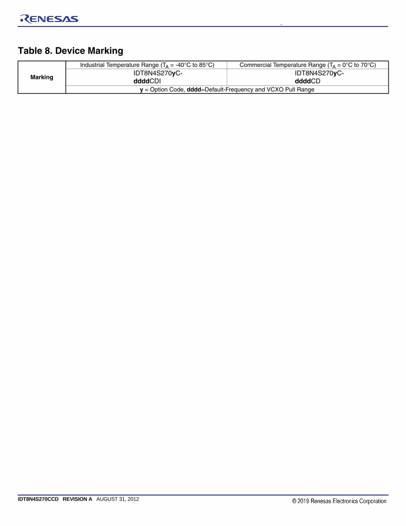
Table 8. Device Marking
Marking
Industrial Temperature Range (TA = -40°C to 85°C) Commercial Temperature Range (TA = 0°C to 70°C)IDT8N4S270yC-ddddCDI
IDT8N4S270yC-ddddCD
y = Option Code, dddd=Default-Frequency and VCXO Pull Range

IDT8N4S270 Data Sheet LVDS FREQUENCY-PROGRAMMABLE CRYSTAL OSCILLATOR
DISCLAIMER Integrated Device Technology, Inc. (IDT) and its subsidiaries reserve the right to modify the products and/or specifications described herein at any time and at IDT’s sole discretion. All information in this document, including descriptions of product features and performance, is subject to change without notice. Performance specifications and the operating parameters of the described products are determined in the independent state and are not guaranteed to perform the same way when installed in customer products. The information contained herein is provided without representation or warranty of any kind, whether express or implied, including, but not limited to, the suitability of IDT’s products for any particular purpose, an implied warranty of merchantability, or non-infringement of the intellectual property rights of others. This document is presented only as a guide and does not convey any license under intellectual property rights of IDT or any third parties.
IDT’s products are not intended for use in applications involving extreme environmental conditions or in life support systems or similar devices where the failure or malfunction of an IDT product can be reasonably expected to signifi-cantly affect the health or safety of users. Anyone using an IDT product in such a manner does so at their own risk, absent an express, written agreement by IDT.
Integrated Device Technology, IDT and the IDT logo are registered trademarks of IDT. Other trademarks and service marks used herein, including protected names, logos and designs, are the property of IDT or their respective third party owners.
Copyright 2012. All rights reserved.
6024 Silver Creek Valley Road San Jose, California 95138
Sales800-345-7015 (inside USA)+408-284-8200 (outside USA)Fax: 408-284-2775www.IDT.com/go/contactIDT
Technical [email protected]+480-763-2056
We’ve Got Your Timing Solution
Corporate HeadquartersTOYOSU FORESIA, 3-2-24 Toyosu,Koto-ku, Tokyo 135-0061, Japanwww.renesas.com
Contact InformationFor further information on a product, technology, the most up-to-date version of a document, or your nearest sales office, please visit:www.renesas.com/contact/
TrademarksRenesas and the Renesas logo are trademarks of Renesas Electronics Corporation. All trademarks and registered trademarks are the property of their respective owners.
IMPORTANT NOTICE AND DISCLAIMER
RENESAS ELECTRONICS CORPORATION AND ITS SUBSIDIARIES (“RENESAS”) PROVIDES TECHNICAL SPECIFICATIONS AND RELIABILITY DATA (INCLUDING DATASHEETS), DESIGN RESOURCES (INCLUDING REFERENCE DESIGNS), APPLICATION OR OTHER DESIGN ADVICE, WEB TOOLS, SAFETY INFORMATION, AND OTHER RESOURCES “AS IS” AND WITH ALL FAULTS, AND DISCLAIMS ALL WARRANTIES, EXPRESS OR IMPLIED, INCLUDING, WITHOUT LIMITATION, ANY IMPLIED WARRANTIES OF MERCHANTABILITY, FITNESS FOR A PARTICULAR PURPOSE, OR NON-INFRINGEMENT OF THIRD PARTY INTELLECTUAL PROPERTY RIGHTS.
These resources are intended for developers skilled in the art designing with Renesas products. You are solely responsible for (1) selecting the appropriate products for your application, (2) designing, validating, and testing your application, and (3) ensuring your application meets applicable standards, and any other safety, security, or other requirements. These resources are subject to change without notice. Renesas grants you permission to use these resources only for development of an application that uses Renesas products. Other reproduction or use of these resources is strictly prohibited. No license is granted to any other Renesas intellectual property or to any third party intellectual property. Renesas disclaims responsibility for, and you will fully indemnify Renesas and its representatives against, any claims, damages, costs, losses, or liabilities arising out of your use of these resources. Renesas' products are provided only subject to Renesas' Terms and Conditions of Sale or other applicable terms agreed to in writing. No use of any Renesas resources expands or otherwise alters any applicable warranties or warranty disclaimers for these products.
(Rev.1.0 Mar 2020)
© 2020 Renesas Electronics Corporation. All rights reserved.