a new embedded package structure and technology … semicon...a new embedded package structure and...
TRANSCRIPT

A New Embedded Package Structure and Technology for Next Generation of WLP,
Wide Strip Panel Fan-out Package - WFOPTM J-DEVICES CORPORATION
Packaging Research & Development Center
Akio Katsumata

Contents
1. J-DEVICES’ Semiconductor Packaging Roadmap
2. J-DEVICES’ FO-WLP Development Concept
3. WFOPTM Technology
4. WFOPTM Characteristic
5. a- WFOPTM Technology
6. Conclusion
About J-DEVICES

About J-DEVICES
Foundation ・Established with capital from NAKAYA Micro Devices, Amkor and Toshiba in 2009. ・Merged Fujitsu Semiconductor’s assembly and test division in 2012. ・Merged Renesas three assembly and test factories in this June. Goal ・To become one of the leading global companies in the semiconductor backend business. Focus ・R&D is focused on developing new connecting technologies and has the experience to manufacture using new connecting technologies. ex. Three years experience with 40um bump pitch CoC manufacturing. ・Automotive product experience
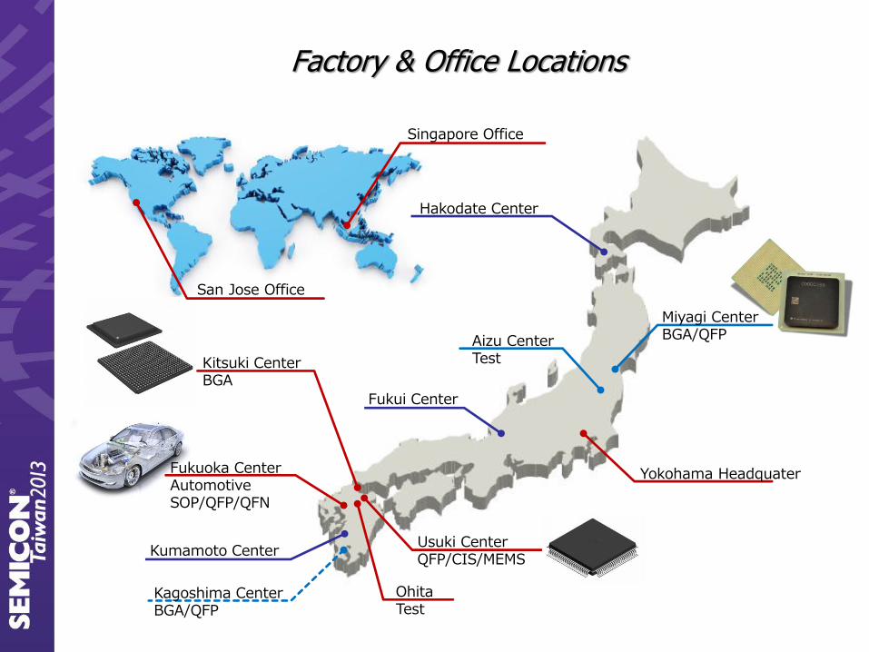
Factory & Office Locations
Aizu Center Test
Yokohama Headquater
Usuki Center QFP/CIS/MEMS
Ohita Test
Kitsuki Center BGA
Fukuoka Center Automotive SOP/QFP/QFN
Kagoshima Center BGA/QFP
Fukui Center
Kumamoto Center
Miyagi Center BGA/QFP
Singapore Office
San Jose Office
Hakodate Center

OSAT World Wide Ranking
6 9
J-DEVICES will be #5 OSAT and keep growing
Based on the data from Gartner Market Share: Semiconductor Assembly and Test Services, Worldwide, 2011
5

J-DEVICES’ Semiconductor Packaging
Roadmap

J-DEVICES’ Package Roadmap
St-MCP
VQON QON
QFN (Dual Row) HQFP
2000 2004 2010 2006
Year
2008 2002 2012 2014
QFN
20xx
TEBGA
TSV
MAP Type PBGA
LQFP
PBGA
E-BGA
FBGA
St-LQFP
THQFP
CoC C4
Bump connection
Wire Connection RDL
WFOP 3D WFOP
Number of Interconnect
• The technology requirements for semiconductor packages for example higher data transfer, lower thermal resistance and higher reliability are increasing. • Bump connection and RDL are key technologies to realize the next generation semiconductor packages.
J-DEVICES’ FO-WLP Development Concept
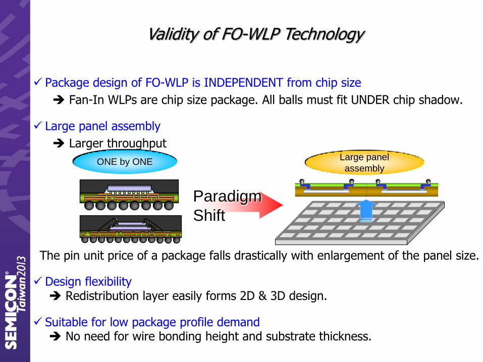
Validity of FO-WLP Technology
Package design of FO-WLP is INDEPENDENT from chip size
Fan-In WLPs are chip size package. All balls must fit UNDER chip shadow.
Large panel assembly
Larger throughput
The pin unit price of a package falls drastically with enlargement of the panel size.
Design flexibility Redistribution layer easily forms 2D & 3D design.
Suitable for low package profile demand No need for wire bonding height and substrate thickness.
Paradigm
Shift
ONE by ONE Large panel
assembly
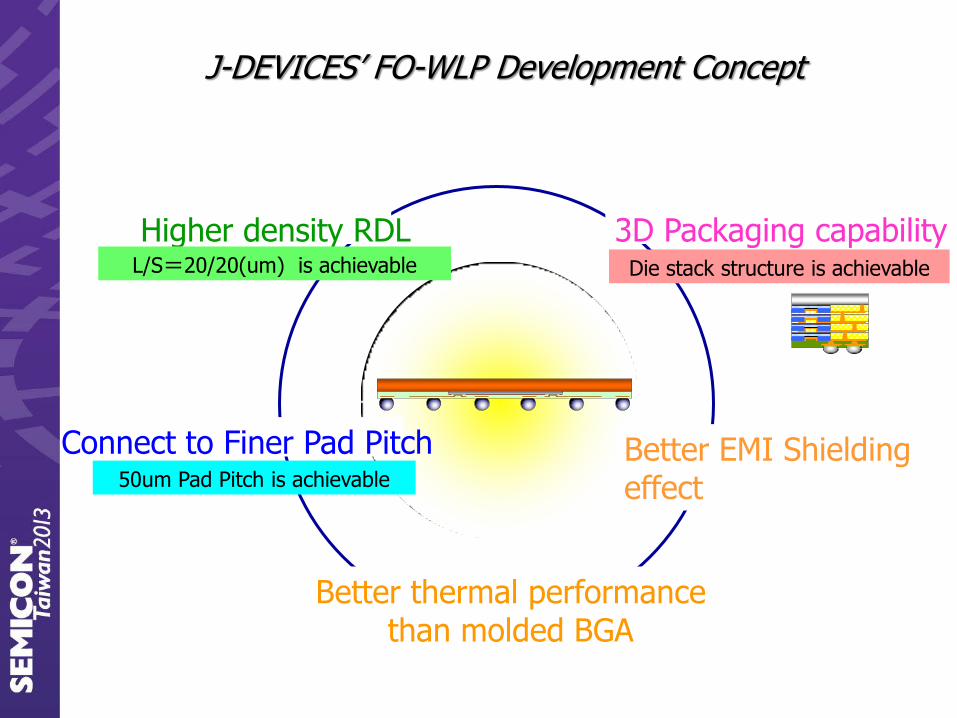
J-DEVICES’ FO-WLP Development Concept
Connect to Finer Pad Pitch 50um Pad Pitch is achievable
Higher density RDL L/S=20/20(um) is achievable
Better thermal performance than molded BGA
Better EMI Shielding effect
3D Packaging capability Die stack structure is achievable
WFOP TM Technology
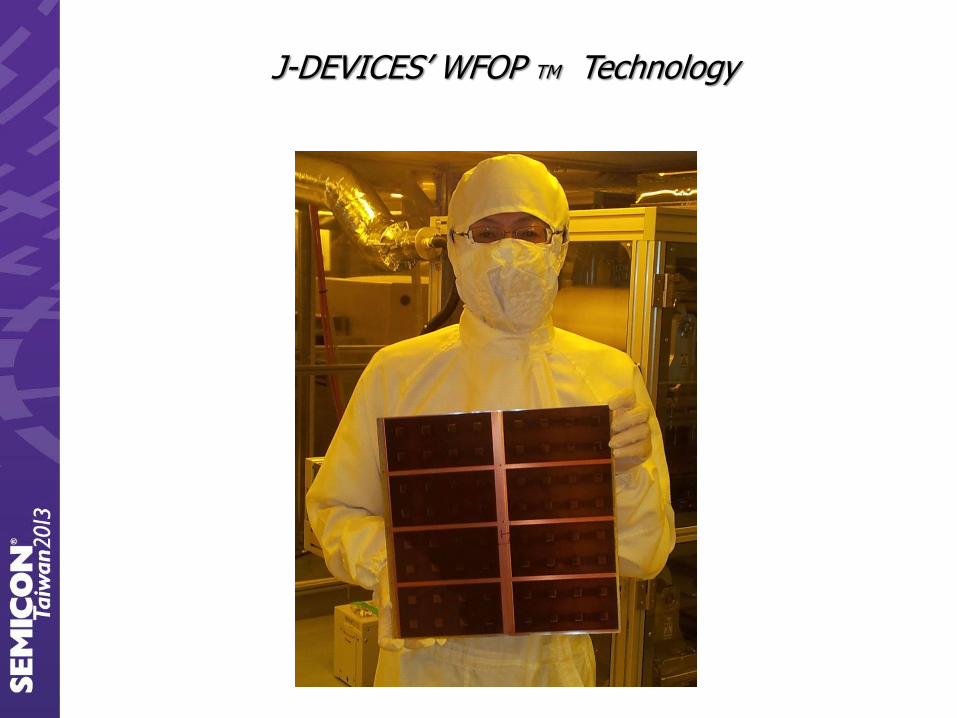
J-DEVICES’ WFOP TM Technology
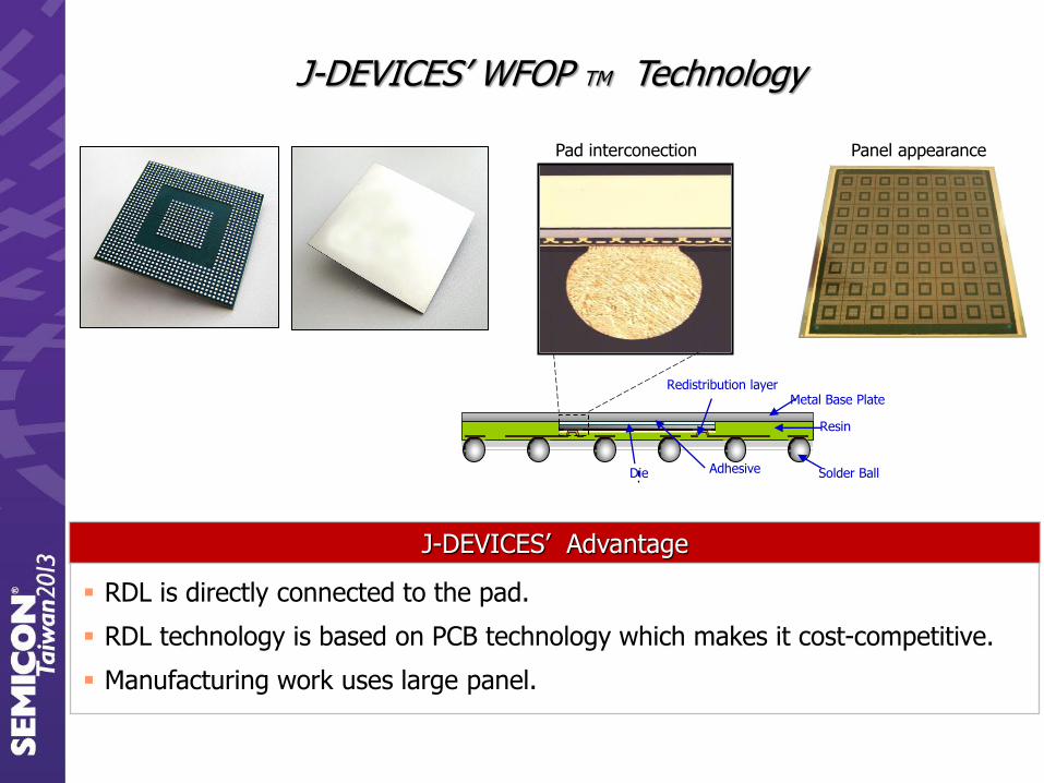
J-DEVICES’ WFOP TM Technology
Pad interconection
Resin
Metal Base Plate
Die Solder Ball
Redistribution layer
Adhesive
Panel appearance
J-DEVICES’ Advantage
RDL is directly connected to the pad.
RDL technology is based on PCB technology which makes it cost-competitive.
Manufacturing work uses large panel.
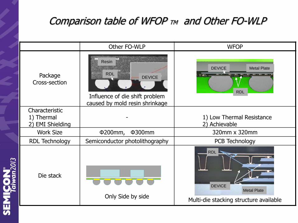
Comparison table of WFOP TM and Other FO-WLP
Other FO-WLP WFOP
Package Cross-section
Influence of die shift problem caused by mold resin shrinkage
Characteristic 1) Thermal 2) EMI Shielding
-
1) Low Thermal Resistance 2) Achievable
Work Size Φ200mm, Φ300mm 320mm x 320mm
RDL Technology Semiconductor photolithography PCB Technology
Die stack
Only Side by side
Multi-die stacking structure available
DEVICE Metal Plate
RDL
DEVICE Metal Plate
RDL
DEVICE
Resin
RDL

J-DEVICES’ WFOP TM Technology
Metal Plate
Die
Redistribution layer Adhesive
Solder Ball Resin
Pad interconection
Via-connection Technology
•Deep Via is realized by laser technology. •Multi-RDL are easy to formed using PCB technology. • No need for bump and package substrate. • Like core-less substrate structure. Reduced capacitance and inductance of wiring.
Material Thickness (Height)
Metal base plate 300um
Ball Stand-off (1mm pitch)
500um
Die 50um
Cu wiring 12um
Interlayer insulator 18um
RDL 2layers RDL 3layers
Package Total Height
935um 965um

Design Rule to connect Area Pad
Via (Interlayer connect) Ball land
E
F G
H
Pad connect (Area pad)
C
D I
K
J K’
Zoom
Die
Die pad
Pad opening (opening separately)
L1 Cu pattern
Via land (adjacent solder ball)
Symbol Item
Design value
Current Next generation
Option-1 Option-2
Line width 20um 20um 15um
Line space 20um 20um 15um
C Die pad opening diameter 50um 30um 35um
D Via land diameter 80um 60um 65um
E Via land diameter 80um 60um 65um
F Via diameter 50um 30um 35um
G Via land -line space 20um 20um 15um
H Via pitch 100um 80um 80um
I Ball land diameter Refer other page
J Ball land - line space 20um 20um 15um
K Ball land – via land space (Same NET)
0um
K’ Ball land – via land space (Different NET)
20um 20um 15um

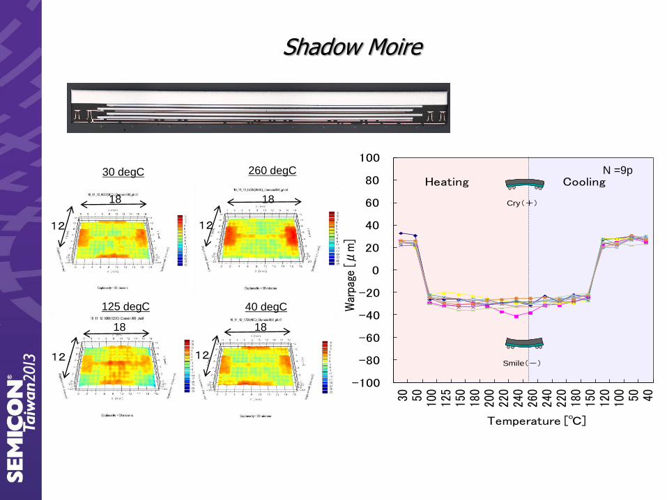
Shadow Moire
-200
-180
-160
-140
-120
-100
-80
-60
-40
-20
0
20
40
60
80
100
120
140
160
180
200
30
50
100
125
150
180
200
220
240
260
240
220
180
150
120
100 50
40
War
page
[μ
m]
Temperature [℃]
1-1 1-3 1-4
Heating Cooling30 degC
125 degC
260 degC
40 degC
Cry(+)
Smile
(-)
35mm
35mm
Resin’s Tg =130 degC
and 150deg. So the
profile changes so much
here.

Package Reliability Test Result
No failure was observed under these test conditions.
Item Test Conditions
Test Result(NG)
100cyc
/168h
300cyc
/312h
500cyc
/500h
700cyc/
712h
1000cyc
/1000h
TCT
MRT1+TCT -55degC/125degC 0NG/22 0NG/22 0NG/22 0NG/22 0NG/22
MRT2+TCT -55degC/125degC 0NG/11 0NG/11 0NG/11 0NG/11 0NG/11
PCT
MRT1+PCT 110degC/85%/1.2atm 0NG/22 0NG/22 0NG/22 0NG/22 0NG/22
MRT2+PCT 110degC/85%/1.2atm 0NG/10 0NG/10 0NG/10 0NG/10 0NG/10
HTS MRT1+HTS 150degC 0NG/22 0NG/22 0NG/22 0NG/22 0NG/22
MRT1:30degC/70%/216h+Reflow4times
MRT2:30degC/70%/144h+Reflow+30degC/70%/96h+Reflow
PKG WFOP900-35x35-1.00
ChipSize 10.00mm x 10.00mm
Al Pad Size 100um
Pad Opening 65um
UBM Size 86um
Pad Pitch 150um
Test Vehicle
WFOP TM Characteristic

Thermal Characteristic of WFOP TM
10.0
15.0
20.0
25.0
30.0
35.0
40.0
0.0 5.0 10.0
θJA
[degC
/W]
Die size [sq.mm]
0.0
2.0
4.0
6.0
8.0
10.0
12.0
14.0
0.0 5.0 10.0θ
JC
[degC
/W]
Die size [sq.mm]
⊿40%
⊿15%
⊿67%
⊿84%
FBGA WFOPTM
WFOP
FBGA
WFOP
FBGA
Motif Body size : 17mm□ Ball counts : 529pin Metal plate : Cu @WFOP
• The thermal resistance of WFOPTM is decreased because metal plate effectively functions as a heat-spreader.

WFOP TM :“EMI shielding” Effect of Metal Plate
WFOP
FBGA
-120
-100
-80
-60
-40
-20
0
-25 -5 15
Ma
gn
etic f
ield
[d
BA
/m]
X coordinate [mm]
WFOPFBGA
Simulation results (Magnetic field)
Package size : 12 x 18mm Die size : 1.4 x 4.5mm Frequency : 1GHz
X-Z plane
Package
Package
-40dB
RDL
Power feeding
Bonding wire
Power feeding
• The better shielding effect of WFOPTM is verified by simulation.

WFOP TM :“EMI shielding” Effect of Metal Plate
-40
-20
0
20
40
60
80
-25 -15 -5 5 15 25
X coordinate[mm]
Ele
ctr
ic f
ield
[d
B]
WFOP
FBGA
Simulation results (Electric field)
Package size : 12 x 18mm Die size : 1.4 x 4.5mm Frequency : 1GHz
X-Z plane
Package
Package
-76dB
RDL
Power feeding
Bonding wire
Power feeding
• The better shielding effect of WFOPTM is verified by simulation.

a-WFOP TM Technology

a-WFOP TM for Finer PAD Pitch
Pad interconection
Resin
Metal Plate
Die Solder Ball
Redistribution layer Adhesive
• Finer inter-connection to device is realized by Lead-finger technology. • J-DEVICES already developed 50um PAD pitch interconnection technology.

Design Rule to connect Finer PAD Pitch
Current Design Rule Next generation
Die
Die pad
Pad opening (opening collectively)
L1 Copper pattern L/S = 20um/ 20um
Via land [80um dia.] (adjacent solder ball)
50um
50um pitch 45um pitch
Die
Die pad
Pad opening (opening collectively)
L1 Copper pattern L/S 15um/ 15um*1 18um/ 18um*2
Via land [70um*1/ 65um*2 dia.] (adjacent solder ball)
45um
*1:option-1 ,*2:option-2

a-WFOP TM for Die Staked Sturcture
• Enables “Die stack module” without TSV structure. • Enables higher multi-channel memory module without customized memory devices. • Lower Thermal Resistance and high EMI shielding performance.
Material Thickness (Height)
Metal base plate 300um
Ball Stand-off (1.0mm pitch)
320um
Die 50um
Cu wiring 15um
Interlayer insulator 15um
RDL 3layers
Package Total Height
1055um
Die
Shadow Moire
-100
-80
-60
-40
-20
0
20
40
60
80
100
30 50 100
125
150
180
200
220
240
260
240
220
180
150
120
100 50 40
War
page
[μm
]
Temperature [℃]
Heating Cooling
Cry(+)
Smile(-)
N =9p
12
18
12
18
12
18
12
18
30 degC
125 degC
260 degC
40 degC

Conclusion

Conclusion
•The technology requirements for semiconductor packages for example higher data transfer, lower thermal resistance and higher reliability are increasing. Bump connection and RDL are key technologies to realize next generation packages. •Panel scale assembly is a new solution to change the packaging manufacture style. (from One by One to Panel assembly) •The development concept of WFOPTM is connect to finer pad pitch, better thermal performance, better EMI shielding and 3D packaging capability. •Internal reliability test was already finished. J-DEVICES is promoting this technology for next generation devices.

END