a new offset cancellation technique for temperature
TRANSCRIPT

A new offset cancellation
technique for temperature sensors
&
Design of 8-bit decimation filter
for biomedical applications
-Harsh Shakrani-
A Dissertation Submitted to
Indian Institute of Technology Hyderabad
In Partial Fulfillment of the Requirements for
The Degree of Master of Technology
Department of Electrical Engineering
June, 2018

ii
Declaration
I declare that this written submission represents my ideas in my own words, and where others’
ideas or words have been included, I have adequately cited and referenced the original
sources. I also declare that I have adhered to all principles of academic honesty and integrity
and have not misrepresented or fabricated or falsified any idea/data/fact/source in my
submission. I understand that any violation of the above will be a cause for disciplinary action
by the Institute and can also evoke penal action from the sources that have thus not been
properly cited, or from whom proper permission has not been taken when needed.
(Signature)
HARSH SHAKRANI
(– Student Name –)
EE16MTECH11022
(Roll No)

iii

iv
Acknowledgements
I would like to thank my parents for giving me this life. I couldn’t have achieved anything
without their support and I am indebted to them all life. Next I would thank my guide
Dr.Ashudeb Dutta for giving me an opportunity to do project under his guidance, supporting
me throughout my M.Tech in getting good subject knowledge, providing many resources to
learn. I would like to thank my senior Prakash Kumar lenka who guided me in my project and
making me clear with many concepts. I take this opportunity to express my happiness for
getting a caring Seniors like Pravanjan Patra, Indranil bhatacharjee, Murli Krishnan,Pankaj
Kumar Jha & Narendra Nath Ghosh in IIT. Last but not the least I would like to thank my
friends Indranil bhatacharjee and ekta prajapati for allowing me to share many happy and
sad moments with them.
I thank IIT Hyderabad for giving me all facilities, Opportunities and resources for completing
my Masters and helping for me to grow as Human.

v
Abstract
In our day to day life there are lot of things which we need to sense and then decide the course
of action according to it. Many of these can be physically sensed easily, but the exact value
of the sensed cannot be determined by human. There will be a lot of error in judged value and
exact value. So instead of human sensing them and judging the exact value there are physical
instruments which can provide lot more accurate value of sensed item than human, which are
called SENSORS.
There are lot of different sensors for sensing different things and one of prominent one is
temperature sensor. Temperature sensor plays an important role in many applications. For
example, maintaining a specific temperature is essential for equipment used to fabricate
medical drugs, heat liquids or clean other equipment. For application like these, the accuracy
of detection can be critical.
The work done in this Thesis shows how to maintain the accuracy of temperature sensor.
Temperature sensor used here is a Wheatstone bridge circuit consisting of two resistors and
two thermistors. Mismatch between the resistors or thermistors will lead to incorrect detection
of value, which is called OFFSET, therefore to maintain the accuracy the mismatch has to be
minimized or removed. One of the Technique to minimize the offset and results pertaining to
it has been displayed in this Thesis.
Technique described in this Thesis consist of first sensing the difference between resistors
value, one being the reference resistor and other the on-chip resistor used in temperature
sensing, second amplifying the difference of resistor value using OPAMP, third sending the
amplified signal to single ended SAR ADC, which gives digital bits as output. And according
to the digital output changing resistor value using resistor switching method. Thus then this
resistor will be used in wheat stone bridge temperature sensing.
The work proposed here can increase or decrease on-chip resistor value depending on
reference resistor. The wheat stone bridge Resistor can be changed by plus minus 5K ohms
with respect to reference resistor.
This is a onetime calibration technique used before start of sensing temperature. After the
resistor have been calibrated, these resistors are used in wheat stone bridge along with
thermistor to sense temperature and the differential output obtained through wheat stone is

vi
passed on to the dual ended SAR ADC, which gives digital representation of temperature
sensed.

vii
Contents
Declaration .......................................................................................................................... ii
Approval Sheet .....................................................................................................................
Acknowledgements............................................................................................................ iv
Abstract ............................................................................................................................... v
1 Introduction ........................................................................................................................ 1
1.1 Temperature sensing ……….…………………..…………………………………...1
1.2 Sensing Element ………..….………………………………………………………..2
1.3 Sensing Circuit………..….………………..…………………………………..3
1.4 SAR ADC…………………………..………………………………………..5
1.5 Offset Cancellation…………………………………………………………..6
2 Offset cancellation Technique ........................................................................................... 8
2.1 Offset cancellation block…………………………………………………….8
2.2 Sensing Resistor mismatch…………………………………………………..9
2.3 Amplifying the sensed signal……………………………………………….11
2.4 Combining Resistor mismatch circuit and op-amp circuit …………..…….15
3 SAR ADC………………………………………………………………….......................19 3.1 Analog to digital conversion …………………………….………………….19
3.2 Successive Approximation ADC Algorithm……… ……………………....19
3.3 SAR BLOCK………………………………..……………………………….20
3.4 Working of capacitor DAC …………………………………………..…….22
4Reconfiguring resistors………… ……………………………………………………….25
4.1 Method of reconfiguring the resistor …………….………………………….26
4.2 Set of resistors…….……………………………………………………......27
4.3 Adding resistors ………………….…………………..…………………….28
4.4 Reconfiguring………………………….……………………………..…….30
4.4 Both increasing and decreasing the resistance ……..………………..…….34

viii
5 Decimator………………………………………………………………………………325
5.1 Need of decimator …………….……………………………………………36
5.2 Sigma Delta ADC …….………………………….……………………......36
5.2.1 Advantages of Sigma Delta ADC ………………….……………...36
5.3 Sigma delta ADC instead of SAR ADC in Offset cancellation block …….39
5.4 Decimation theory …………………………………………………………..39
5.4.1 Need of Filter in Decimator ………………….…….……………...41
5.5 Filter Architecture…………………………………………………...……..42
5.6 Filter Design …………………………………………………………..…..44
5.4.1 Selection of filter ………………….…….……………...................45
5.7 Design in Simulink and in Verilog ………………………………....……..48
6 Results and conclusion …………………………………………….……………………49
6.1 Offset cancellation block result …………….………………………………49
6.2 Decimator Result …….………………………….………………………....50
6.2.1 First Sinc Filter Output …………….……………….……………...51
6.2.1 Second Sinc Filter Output …………….…………….……………...51
6.2.1 Third Sinc Filter Output …………….……..……….……………...52
6.2.1 Fourth Sinc Filter Output …………….…………….……………...52
References ............................................................................................................................ 53

1
Chapter 1
Introduction:
1.1 Temperature sensing
Temperature sensing is one of the most sensitive properties or parameters for industries
like petrochemical, automotive, aerospace and defense, consumer electronics and so on.
Temperature sensing in most cases is done to display the temperature of given system
or to take control action after detecting temperature. For an example consider a system
such as liquid measuring equipment. Temperature in this case, directly affects the
volume measured. By taking temperature into account, the system can compensate for
changing environment factors, enabling it to operate reliably and consistently.
Temperature sensing is also used as a part of preventative reliability. For example,
consider an appliance that may not actually perform any high temperature, due to the
risk of overheating. Thus as temperature reaches a threshold of overheating, the system
has to start taking preventive action such as cooling the system or partially/ totally
shutting down the system, as per system requirement.
Thus accuracy of sensing temperature is an important task in all situation, because
having even a small error may lead to disastrous situation. Error generated by system
may be either because of sensing circuit or circuit which converts the sensed signal from
one form(analog) to other (digital) form.
Here in this Thesis, error generated due to the sensing circuit is considered and way to
resolve the error is proposed.

2
1.2 Sensing Element
The accurate measurement of temperature is vital across a broad spectrum of human
activities, and also temperature is one of the key parameters which has to be measured
precisely and accurately in industry, healthcare, aerospace etc. Thus important part of
sensing circuit is sensor itself. Some of the sensors are thermocouple, RTD (Registered
temperature detectors) and thermistors, and each one has some pros and cons.
Temperature sensor which is chosen is Thermistor. Thermistor are cheaply available
sensors which work over very low temperature range. Though they have non-linear
characteristics they are known for their sensitivity. Because of their tolerances, these
devices can be replaced by a part of same type and still retain their accuracy. In other
word they are interchangeable.
Modeling thermistor: Thermistor was modelled in cadence using Verilog-A model.
The general relation between temperature of a material having negative coefficient and
its resistance is given by stein-hart equation.
Where
T is temperature in kelvin
R is resistance at T temperature
A, B and C are stein hart coefficient which vary according to type of Thermistor
model.
The thermistor used here is governed by auxiliary stein hart equation given by
Where value of R0, B and T0 have been obtained from set of resistance and temperature
value
R0 = 69.2 K-ohm.
B = 1078.1 deg-kelvin.
T0 = 297.1304 kelvin.
R= 𝑅0𝑒𝐵(1
𝑇−
1
𝑇0)

3
Figure 1.1 : Resistance VS temperature graph.
1.3 Sensing Circuit
Non-linear characteristics between resistance and temperature curve, leads us to that
thermistor cannot be the only element in a temperature sensing circuit.
To obtain proper/accurate result with respect to temperature, the graph between
resistance and temperature has to be a linear graph, thus there has to a be circuit which
contains some other element along with thermistor as one of the element to sense the
temperature.
One of the circuit which can give accurate output is wheat-stone bridge circuit, it
consists of two thermistors and two resistors.
Wheatstone bridge is one of the widely used signal conditioning circuit for the
resistance change to voltage change conversion. Wheatstone bridge illustrate the
concept of a difference measurement, which can be extremely accurate.

4
Figure 1.2 : Wheatstone bridge circuit.
The right choice of Wheatstone bridge Reference resistor helps in Linearizing the
curve of resistor vs temperature. Figure 1.3 shows the formula used to obtain
reference resistor value, figure also shows whole temperature sensing circuit with
20pF capacitor which will be used as load. And Fig 1.4 shows result of linearized
curve between resistor and temperature after using Linearized resistor.
Figure 1.4: Wheatstone bridge with linearized resistor.
Rth Rref
Rref Rth
GND
VDD
V+V-

5
Figure 1.4: Resistance VS temp graph after using linearized resistor value.
1.4 SAR ADC
The differential output obtained from the Wheat stone bridge, which is in the form of
analog signal has to be converted to digital form, and this is done using Analog to digital
converter (ADC). Depending on specification of input and output signals, type of ADC
is chosen. Here successive approximation register (SAR) is used. SAR ADC is used for
low to medium speed and medium to high resolution applications.
SAR ADC executes conversion in multiple clock cycles, using the information of
previously determined bits. Block diagram of SAR ADC consists of four main blocks:
sample and hold circuit, comparator, DAC and SAR logic.
The Sample and hold circuit samples the input continuous Analog signal on the first
cycle of the clock and then holds the same value for remaining clock cycles. The
comparator compares the sampled and hold value with the reference voltage Vref and
displays the value according to it. SAR logic reconfigures itself after every cycle,
according to the comparator output .
And according to SAR logic value the capacitor DAC value is reconfigured and then
used as one of the input of the comparator.
SAR ADC input signal can be either single ended or fully differential ended. A fully
differential ended input signal has several advantage over the single ended SAR ADC.

6
In fully differential ended SAR ADC the two inputs are 180º out of phase and difference
in voltage signal is considered. Due to this the dynamic range of has doubled and thus
leading to doubling of 𝑉𝐿𝑆𝐵, which indirectly leads to less constraint on design of
comparator. While in the single ended SAR ADC signals are referred with respect to
ground. Thus leading to less dynamic range because of DC offset and noise through the
channel. While in fully differentially ended SAR ADC the noise gets cancelled because
of differential ended structure. Another advantage of over single ended input is that it
reduces the effect of charge injection caused by parasitic capacitor, hence precision
improves.
[ Temperature sensor was designed by previous student, the next defines my work and above
this line the work was done by other person].
1.5 Offset Cancellation
Offset is an undesirable voltage obtained in many circuitry, its obtained due to mismatch
of elements in the circuits. It is generally measured by shorting the input and checking
the value at the output. Thus the signal will ride on DC plus offset value. Although these
voltage value will be very small but will have a considerable effect in many circuits.
And in temperature sensing even a small change in voltage level read or any offset
present can have considerable damage caused.
Offset in Wheatstone bridge circuit will be present because of mismatch of elements.
Thus mismatch can be present because of resistors mismatch or mismatch present
because of thermistor. This thesis presents a way in which, mismatch between resistors
can reduced.
Here the difference between the resistor is sensed and then the sensed signal is then
passed through the amplifier to get the amplified value. This amplified signal is then
digitised using single ended input SAR ADC. And according to the digital bits the
resistors value is changed or adjusted.
Figure 1.6 shows architectural level block diagram of temperature sensor circuit along
with SAR ADC and Offset cancellation block.

7
Fig 1.6 : block diagram of temperature ckt along with offset cancellation.

8
Chapter 2
Offset cancellation Technique
Offset in Wheatstone bridge circuit will be present because of mismatch of elements.
Elements present are resistor and thermistor. Thus offset will be present because of
resistors mismatch or mismatch present because of thermistor. This thesis presents a
way in which, mismatch between resistors can reduced.
2.1 Offset cancellation block
Figure 2.1 shows block diagram of technique used for cancelling the offset. Here the
difference between the resistor is sensed and then the sensed signal (V+ minus V-) is
then passed through the amplifier with gain of Av to get the amplified value at the output
of amplifier.
Vo(amplifier) = Av*(V+ - V-)
The signal is amplified so that it can be easily be digitised by SAR ADC wit good
resolution. This amplified signal is then digitised using single ended input SAR ADC.
And according to the digital bits the resistor R1 value is increased or decreased, so that
the final value is equal to Rref resistor.
The changed resistor R11, which is equal to Rref is then used in Wheat stone bridge
along with the thermistor for temperature sensing. Then Wheat stone bridge gives
differential output, the output obtained will not contain any offset value because of the
mismatch of resistors and then this differential output is then passed on to the Fully
differential ended SAR ADC. ADC’s output is in discretised form which is then used
for required purpose.
The SAR ADC used in offset cancellation is a single ended SAR ADC unlike the ADC
which uses differential ended in main temperature sensing block.

9
Figure 2.1: Offset cancellation block
2.2 Sensing Resistor mismatch
Resistor is not a physical quantity like current and voltage which can be measured
easily. The resistor value has to be converted to these physical quantities which can be
measured. Thus two different resistors are given same current sources and voltage
across the resistor is measured, therefore difference in their resistor is converted to
difference in voltages.
10
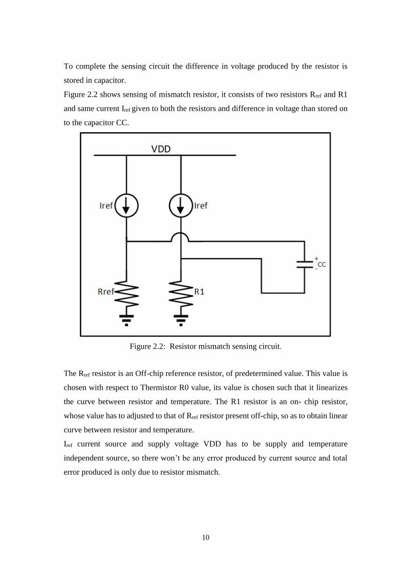
To complete the sensing circuit the difference in voltage produced by the resistor is
stored in capacitor.
Figure 2.2 shows sensing of mismatch resistor, it consists of two resistors Rref and R1
and same current Iref given to both the resistors and difference in voltage than stored on
to the capacitor CC.
Figure 2.2: Resistor mismatch sensing circuit.
The Rref resistor is an Off-chip reference resistor, of predetermined value. This value is
chosen with respect to Thermistor R0 value, its value is chosen such that it linearizes
the curve between resistor and temperature. The R1 resistor is an on- chip resistor,
whose value has to adjusted to that of Rref resistor present off-chip, so as to obtain linear
curve between resistor and temperature.
Iref current source and supply voltage VDD has to be supply and temperature
independent source, so there won’t be any error produced by current source and total
error produced is only due to resistor mismatch.

11
2.3 Amplifying the sensed signal.
The sensed signal which is stored in capacitor CC as shown in fig 2.2 has to be
amplified, such that the signal can be easily be discretised by SAR ADC and it obtains
a good resolution. The amplifier gain has to be decided on the basis of maximum range
of resistor difference which can be present between Rref and R1 resistors and it also
depends on gain of amplifier, this constraint is decided by the designer. The formula for
the maximum value of resistor is shown below.
Where
VDD and VEE are rail to rail voltage railing between which amplifier can
operate. In this case it is from 1v to 0v respectively.
Rref is the reference resistor which is an off chip resistor.
Gain is the amplifier gain (Av).
R1 is a variable resistor whose maximum value can go up to R1max, this value
depends upon the value of amplifier gain (Av), and its value is chosen such that
the output of amplifier just saturates, that is it reaches VDD or VEE.
By using above formula where VDD and V is equal to 1v and 0v, and the current source
of 1u A with respect to fig 2.2 if chosen, and gain of amplifier is 100, we can vary upto
plus and minus 5K ohms of R1 resistor with respect to Rref resistor.
The amplifier chosen here is an Operational amplifier (Op-amp) whose gain is
considered to be very high, and has negative feedback present. Since Op-amp has high

12
gain and has negative feedback present the gain of amplifier is roughly equal to the
inverse of feedback factor (1/ beta), where beta is feedback factor.
As shown in fig 2.3 the capacitor CC which had stored the difference of resistors Rref
and R1 in terms of voltage is directly connected to the Op-amp with the gain of Av, the
output obtained won’t be equal to Av* Vcc, where Vcc is the voltage stored in capacitor
CC.
Fig 2.3: Capacitor CC directly connected to op-amp.
The actual value obtained at the output of op-amp will be Vo1 = Av * (Vcc + Voffset), as
shown in fig 2.4. This Voffset is an offset present because of mismatch of circuit in Op-
amp.
This offset cannot easily be removed by adding extra circuitry, thus this offset will be
present in Op-amp. The extra unwanted voltage present at the output (Av*Voffset) will
lead to inaccurate value at the output of SAR ADC, thus leading to display of wrong
temperature value.
Fig 2.4: CC connected and V-offset taken into consideration.

13
A mechanism has to be considered which removes this offset present in op-amp. There
are few techniques present which can remove the offset present and one the technique
which has be used in this thesis is using switching. This technique is considered in detail
in next section.
Offset less Op-amp
Offset present in the input of Op-amp gets multiplied the gain of op-amp and produces
the in inaccurate value at the output of Op-amp. The Technique which is presented in
this thesis is shown in fig 2.5 and fig 2.6.
Fig 2.5: step 1 – offset voltage stored on capacitor CL.
The technique used in this thesis consist of two major steps.
First step: is shown in fig 2.5. Here the high gain Op-amp is used in Unity gain negative
feedback configuration.
The Bias voltage is applied to the Positive terminal of op-amp, this voltage is used for
DC biasing the Op-amp. Because of negative feedback the virtual short concept applies
and the negative terminal of op-amp will also be biased at Vbias voltage.
One terminal of output capacitor CL is connected to output of op-amp, while other
terminal of op-amp is connected to Vbias voltage.

14
Thus the voltage stored across capacitor CL is Voffset.
Voltage across capacitor CL = 𝑉𝑏𝑖𝑎𝑠 + 𝑉𝑜𝑓𝑓𝑠𝑒𝑡 − 𝑉𝑏𝑖𝑎𝑠
=𝑉𝑜𝑓𝑓𝑠𝑒𝑡
Now this capacitor has to be connected to input in such a way that the offset of op-amp
gets subtracted. The technique is shown in step 2.
Second step: In this step the voltage produced in the previous step on to the capacitor
has to be used in such a way that the offset voltage gets removed. The technique to
remove is shown in fig 2.6.
Fig 2.6: step 2 – op-amp connected as Non inverting configuration, with Capacitor CC
and CL connected in such a way that offset gets cancelled, and Voltage stored in
capacitor CC gets amplified.

15
In this step op-amp is used in non-inverting configuration with negative feedback. The
capacitor CC and CL are connected as shown in fig 2.6. The voltage at the output of op-
amp is given as
Vo2 = Av * V+.
Vo2 = (1 + R2/R1) * V+.
The op-amp here is a high gain op-amp therefore the gain is inverse of feedback factor.
While positive terminal is given as
V+ = Vbias + Vcc – Vcl + Voffset.
V+ = Vbias + Vcc – Voffset + Voffset.
V+ = Vbias + Vcc.
Where V+ consist of both ac and dc signal, although here Vbias and Vcc are Dc quantities.
The output step 2 of op-amp Vo2 is given as
Vo2 = (1+ R2/R1) * Vcc + Vbias.
Vo2 signal is running on Vbias voltage.
Output from step 2 does not consist of V-bias term, and output totally depends on the
gain and Vcc value, indirectly it depends on difference between resistors value.
If the difference between Rref and R1 resistor is positive, then the output of op-amp is
above Vbias voltage and if difference is negative then output value is below Vbias voltage.
The signal gets saturated to VDD or VEE respectively if R1 is above R1max and R1 is
below R1min.
2.4 Combining Resistor mismatch circuit and op-amp circuit.
The total switching circuit diagram between resistor sensing and op-amp offset
cancellation is shown in fig 2.7. The whole system shown in fig 2.7 works on two steps,
first step is when switches which are controlled by V1 are ON and second when
switches which are controlled by V2 are ON. V1 and V2 are non-overlapping signal
with predefined period. Output of this circuitry is the output of op-amp.

16
Fig 2.7: Switching circuitry between resistor sensing circuit and Op-amp cancellation
technique.
Step 1: V1 signal is high and V2 is low, during this the voltage difference created by
resistor mismatch is sensed onto the capacitor CC and op-amp acts like a buffer, similar
to one shown in fig 2.5. The output voltage stored across capacitor CL will be equal to
Voffset. Step 1 is shown in fig 2.8.

17
Fig 2.8: switches with V1 is closed and with V2 is opened.
Step 2: In this step V2 voltage is high, thus switches with V2 are closed and V1 is low
and switches with V1 are opened. Due to this the resistor mismatch circuitry gets
detached and previously voltage stored onto the capacitor CC remains on to it.
Op-amp in this step works in Non inverting configuration with negative feedback
present. The offset voltage which got stored onto the capacitor CL in previous step is
now switched to the input of non-inverting of op-amp in the fashion shown in fig 2.9.
This circuitry is similar to the one shown in fig 2.6. Thus, due to the configuration of
circuit the voltage present at the output of Op-amp will only amplify the voltage stored
on capacitor CC. The offset of Op-amp is cancelled.
Fig 2.9: Switches with V1 open and V2 closed.
The output voltage is then passed on to the SAR ADC, which discretises the output
according to it, and finally output is in digital form(bits).

18
Chapter 3
SAR
3.1 Analog to digital conversion.
To reconfigure the resistor value, resistors value has to be increased or decreased.
Increasing or decreasing the resistor value can be done by adding resistor in series or
add them in parallel. Number of resistors to be added in parallel or in series can be
controlled by using digital signal. Now depending upon the value of the op-amp output
the number of resistors to be added changes, therefore there has to be some conversion
mechanism present which will change the Analog to digital signal, so as to decide no of
resistor present, thus we use ADC.
There are many type of ADC present and depending upon the configuration of signal
and conversion, ADC type is decided. Since here the signal conversion need not be
applied at high rate, therefore SAR ADC is best suited for this circuit.
3.2 Successive Approximation ADC Algorithm.
Successive Approximation algorithm takes N cycle to complete the conversion, if ADC
is of N bits. In this algorithm the input is first compared with Vmid value, where Vmid is
mid value or avg value of Vmax and Vmin (Vmax and Vmin are maximum and minimum
saturate value an ADC can detect, here in the first case Vmax is VDD and Vmin is GND).
Then according to that the next Vmax and Vmin is decided.
Consider if Vin is greater than Vmid, than the next Vmax is VDD and Vmin is Vmid and
Vmid is Avg of Vmax and Vmin. And Vin is than compared with new Vmin and according
to it next Vmid is decided. This cycle repeats its self N cycles, and every cycle sets each
particular bit value according to the comparator output being one or zero.

19
Figure 3.1 shows an example of a 5-bit quantization of input 6.2 using binary successive
approximation search. The solid black lines represent the mid decision level of the
current search range and the solid red line indicates the location of the input level. In
the beginning of the process, the search range is from 0 to 31.
LSB = 𝑭𝒖𝒍𝒍 𝒔𝒄𝒂𝒍𝒆 𝒓𝒂𝒏𝒈𝒆 𝒅𝒚
𝒏𝒐 𝒐𝒇 𝒒𝒖𝒂𝒏𝒕𝒊𝒛𝒂𝒕𝒊𝒐𝒏 𝒍𝒆𝒗𝒆𝒍 =
𝟑𝟐
𝟑𝟐 = 1
During the first comparison, VIN (equal to 6.2) is compared with the mid-full-scale
level of the initial search range. Since 6.2 is less than 16, the ADC outputs a ’0’ and the
search range becomes the lower half of the previous search range. The search process
continues for a total of five clock cycles to produce the final binary output equal to
00110. The last search reduces the range of uncertainty to one LSB, resulting in
quantization error within ±0.5LSB.
Figure 3.1: An Example of binary search using successive approximation algorithm.
3.3 SAR BLOCK
Multiple clock cycles are needed to executes SAR conversion, and each bit is evaluated
using previously determined bits. The block diagram of SAR logic is shown in fig 3.2.
It consists of four main block blocks, Sample and hold circuitry, Comparator, SAR logic
block and Capacitor DAC.

20
Fig 3.1: SAR ADC structure.
The sample and hold circuitry samples the input value in first clock cycle and holds the
same value for remaining cycle of conversion.
Comparator compares Vhold and Vdac value every clock cycle and gives the necessary
output according to it. The comparator output is than given to SAR control logic and
SAR logic reconfigures the particular bit at particular clock cycle, thus giving perfect
output at the end of conversion.
DAC of SAR ADC can be implemented in many ways (R-2R, capacitor, sterling or
hybrid R – C method). For fast conversion of signal in SAR ADC using MOS
technology, using R-2R technique is not the perfect method to do conversion. The
reason is that the proper sheet resistance value is not available in single technology and
this approach requires proper ratio of ON resistance value in MOS switches over a wide
range.
The best way of implementing DAC for this process is by using capacitor array scheme.
It merges both the sample and hold mechanism along with conversion process. The
subtraction of input voltage with Capacitor DAC voltage is done by capacitor in charge
domain.
Compared to conventional R-2R method, Capacitor arrays are easily fabricated and
produces less mismatch error than that of conventional R-2R method. And also
capacitor array saves power by using charge distribution method.

21
3.4 Working of capacitor DAC
The conventional single ended SAR ADC consists of N- bit binary weighted capacitor
DAC, ranging from 20 to 2N-1(Where N is Number of bits in ADC). It also consists of a
Comparator and SAR control logic. Figure 3.3 shows single ended SAR ADC along
with Binary weighted capacitor DAC.
Fig 3.4: Single ended SAR ADC.
As shown in fig 3.4 the bottom plate of capacitor can be connected to either Vin, Vref+
or Vref-. The total capacitance sums up to Ctot, where Ctot is given as
During Sample and hold phase, as shown in fig 3.5, that is during first clock cycle the
capacitor array samples the input by connecting the bottom plate of all binary weighted
capacitor to Vin and top plate connected to ground. The total charge stored across
capacitor is given by
Fig 3.5: Sampling phase in SAR ADC.

22
After sampling the input, we enter into conversion phase. In the first cycle, the most
significant bit of binary weighted capacitor is connected to the Vref+ and all others
capacitor are connected to the Vref- as shown in fig 3.6.
Here for simplicity the Vref+ = VREF and Vref- = 0. And top plate of capacitor (V-)
is connected to the comparator, which is given by
𝑉− = −𝑉𝑖𝑛 + 2𝑁−1𝐶𝑢
𝐶𝑇𝑜𝑡 𝑉𝑅𝐸𝐹 = −𝑉𝑖𝑛 +
𝑉𝑅𝐸𝐹
2
Fig 3.6: First cycle of conversion. 𝟐𝑵−𝟏𝑪𝒖 connected to 𝑽𝑹𝑬𝑭.
The first term in above equation is due to sampling of input during sample mode and
this value remains hold up in capacitor for remaining cycle of conversion. While the
second term in the above equation is due to MSB capacitor.
Now the above value obtained from capacitor DAC is compared with 0.5V, the reason
is that 0.5V is the mid value of VREF+ and VREF-. Thus DAC value above 0.5v, will
lead to comparator giving value equal to 0 and DAC value below 0.5v will lead to
comparator giving value of 1.
Considering comparator output to be equal to 𝑑, Now during first cycle of conversion
(when MSB capacitor 2𝑁−1𝐶𝑢 is connected to 𝑉𝑅𝐸𝐹) if comparator output 𝑑𝑁−1 = 1,
then 2𝑁−1𝐶𝑢 capacitor remains connected to 𝑉𝑅𝐸𝐹 else if comparator output 𝑑𝑁−1 = 0,
then 2𝑁−1𝐶𝑢 capacitor is connected to 𝐺𝑁𝐷. In both the above cases, that is after the

23
first conversion cycle , 2𝑁−2𝐶𝑢 is connected to 𝑉𝑅𝐸𝐹. Both the cases are shown in fig
3.7 and 3.8 respectively.
Fig 3.7: If comparator output 𝒅𝑵−𝟏= 1.
Fig 3.8: If comparator output 𝒅𝑵−𝟏= 0.
The voltage generated by the capacitor DAC in above mentioned cases, is given as
follows.
If 𝑑𝑁−1 = 1, 𝑉− is given as
𝑉− = −𝑉𝑖𝑛 + (2𝑁−1+ 2𝑁−2)𝐶𝑢
𝐶𝑇𝑜𝑡 𝑉𝑅𝐸𝐹 = −𝑉𝑖𝑛 +
3𝑉𝑅𝐸𝐹
4 .

24
If 𝑑𝑁−1 = 0, 𝑉− is given as
𝑉− = −𝑉𝑖𝑛 + (2𝑁−2)𝐶𝑢
𝐶𝑇𝑜𝑡 𝑉𝑅𝐸𝐹 = −𝑉𝑖𝑛 +
𝑉𝑅𝐸𝐹
4 .
Now depending on the above two condition, 𝑉− is compared with respect to 𝑉0.5 v and
the next digital output bit, 𝑑𝑁−2 is decided. This process keeps on continuing and every
digital bit 𝑑𝑁 is generated through comparator. And final 𝑉− value is generated is given
as
𝑉− = −𝑉𝑖𝑛 + ∑ 2𝑑𝑖
𝑁−1𝑖=0 (2𝑖)𝐶𝑢
𝐶𝑇𝑜𝑡 𝑉𝑅𝐸𝐹 −
𝐶𝑢
𝐶𝑇𝑜𝑡 𝑉𝑅𝐸𝐹.
The voltage generated at the end of conversion is the quantization error generated.
There are parasitic capacitance also generated from layout of Top and bottom plate
capacitor. The parasitic capacitances on the bottom plate are driven by low impedance
reference supplies, VREF+ and VREF -- Typically, these do not affect the conversion
process as long as the reference voltages are completely settled. The parasitic
capacitance on the top plate, on the other hand, attenuates the amplitude of sampled
input. The attenuation factor can be calculated as
𝛽 = 𝐶𝑇𝑜𝑡
𝐶𝑇𝑜𝑡+𝐶 𝑝
Where 𝐶𝑃is the total parasitic capacitance on the top plate. This attenuation reduces the
effective signal power, but does not change the polarity of the comparison result, which
is the only relevant information for determining the correct output bits. The bottom-
plate sampling essentially enables this feature. In the sampling phase, the top plate is
pre-charged to ground before the node becomes floating and remains floating until the
end of the conversion phase. During the conversion, the voltage on the top plate moves
but returns to a voltage that is near zero at the end of the process. As a result, the total
charge on 𝐶𝑃 is the same at the beginning and at the end of the process and therefore,
from the perspective of charge, capacitor 𝐶𝑃 does not cause any charge error. Therefore,
it does not affect the overall accuracy of the conversion process.

25
Chapter 4
Reconfiguring resistors
4.1 Method of reconfiguring the resistor
The output of SAR ADC consists of 10 digital bits. These 10 bits are digital output
representation of amplified Analog voltage difference between the two resistors. Now
according to these 10 digital bits, the resistor value has to be reconfigured. Therefore a
mechanism has to be decided which can reconfigure the resistor value easily and
efficiently, through these 10 digital bits.
One way of reconfiguring the resistor is by adding resistor in series or parallel. But the
value of resistor to be added to reconfigure the main resistor is determined by the
voltage difference produced by mismatch of resistors (reference and temperature sensor
resistor), thus every time a different value of resistor has to be added according to
mismatch. And thus selecting these many resistors with less difference between the two
succeeding resistor is an impossible task.
To have less difficulty and to make work easy, we can have set of predetermined
resistors of different value. These resistor value will follow some proportionality
constant. And depending on the resistors mismatch value, we will select resistors from
the set of predetermined resistors. The selected resistors will then be added to the main
resistor so that the resistor reconfiguration can take place.
The number of resistors to be selected and which value of resistor has to be selected is
decided by Digital bit, which are obtained from SAR ADC output. Each bit from digital

26
bit produced is assigned a unique resistor value and depending on the value of bit the
corresponding resistor will be selected or will not be selected.
If 𝑑𝑁−2 = 1 that is the most significant bit is 1, then 𝑅𝑁−2 will be selected and added to
main resistor. Similarly for different bit of 𝑑 the corresponding resistor is selected and
added depending on the value of the bit.
4.2 Set of resistors
The value of resistors in set of predetermined resistors will follow Geometric
Progression (G.P). The reason is that summation of Geometric Progression will lead to
maximum difference (𝑅𝑀𝐴𝑋 − 𝑅𝑅𝐸𝐹) the two resistors can detect. The value of
maximum difference as discussed before depends on the 𝐼𝑅𝐸𝐹 current, which was used
for conversion of resistor to voltage and the Gain of the amplifier.
(𝑉𝐷𝐷−𝑉𝐸𝐸)/2
(𝑅𝑀𝐴𝑋− 𝑅𝑅𝐸𝐹)= 𝐺𝑎𝑖𝑛. (4.1)
(𝑉𝐷𝐷−𝑉𝐸𝐸)/2
𝐺𝑎𝑖𝑛 + 𝑅𝑅𝐸𝐹 = 𝑅𝑀𝐴𝑋 (4.2)
Thus the sum of all resistors used in set of predetermined resistors has to be roughly
equal to maximum difference (𝑅𝑀𝐴𝑋 − 𝑅𝑅𝐸𝐹) between the resistor, which can be
detected.
Thus the resistors have to be (𝑅𝑀𝐴𝑋− 𝑅𝑅𝐸𝐹)
2𝑗 , where j varies from 1 to N-1. Here N is no
of digital bits produced by ADC.
In the case of this work, the (𝑅𝑀𝐴𝑋 − 𝑅𝑅𝐸𝐹) = 5K, this value is decided with the help
of equation (4.1) and (4.2). Thus the resistors present in predetermined set will be 2.5K,
1.25K, 0.625K……and so on.
While the maximum value of resistor has been found out, similarly minimum value of
resistor has to be found out, which can be detected.
(𝑉𝐷𝐷−𝑉𝐸𝐸)/2
(𝑅𝑅𝐸𝐹−𝑅𝑀𝐼𝑁)= 𝐺𝑎𝑖𝑛.

27
𝑅𝑅𝐸𝐹 − (𝑉𝐷𝐷−𝑉𝐸𝐸)/2
𝐺𝑎𝑖𝑛= 𝑅𝑀𝐼𝑁.
Thus if resistor 𝑅 is less then 𝑅𝑅𝐸𝐹 , resistor has to be increased. And if resistor 𝑅 is
more then 𝑅𝑅𝐸𝐹 then the resistor has to be decreased. So in both the cases the resistor
has to be brought to 𝑅𝑅𝐸𝐹 . Where 𝑅𝑅𝐸𝐹 is reference off-chip resistor.
4.3 Adding resistors.
Here in this thesis the temperature sensor resistor can be increased and also can be
decreased, this increase or decrease depends on value of 𝑅 with respect to the 𝑅𝑅𝐸𝐹 .
Thus there has to be mechanism which can decide whether the value of 𝑅 is lesser then
or greater then 𝑅𝑅𝐸𝐹 , and according to it the increase or decrease of 𝑅 can take place.
The MSB bit of ADC decides whether 𝑅 is greater than or lesser then 𝑅𝑅𝐸𝐹 .
Now consider the input of op-amp is biased properly with 𝑉𝑏𝑖𝑎𝑠 voltage and also
considering that 𝑉𝑜𝑓𝑓𝑠𝑒𝑡 voltage to be zero, then the DC output voltage of op-amp will
be constant at particular value. In this case it will be equal to 𝑉𝑏𝑖𝑎𝑠 voltage.
Thus if the resistor 𝑅 is less than the reference resistor 𝑅𝑅𝐸𝐹 , and if the capacitor CC
which stores the difference of resistor value is connected as shown in fig 2.6 and 2.7,
then the positive terminal of op-amp will be above 𝑉𝑏𝑖𝑎𝑠. An op-amp which is
considered here is an noninverting op-amp, gain will be positive and thus the output
value of op-amp in this case will be above 𝑉𝑏𝑖𝑎𝑠.Also consider if the voltage 𝑅 is more
then 𝑅𝑅𝐸𝐹 and capacitor connection is as discussed above, then the op-amp output will
be less then 𝑉𝑏𝑖𝑎𝑠.
And as discussed in SAR ADC chapter MSB bit is high if op-amp output voltage is
above 𝑉𝑏𝑖𝑎𝑠 and MSB is low if output voltage is less then 𝑉𝑏𝑖𝑎𝑠 voltage. Thus leading to
conclusion that the resistor has to be added if MSB is 1 and resistor has to be decreased
is MSB is 0.

28
Controlling resistors
The MSB bit helps in deciding whether the resistor has to be increased or it has to be
decreased. But how can these resistors be added? These resistors are added by using
switching mechanism, and switches are controlled by digital bits produced from ADC
output.
Neglecting the MSB bit, all other N-1 bits helps in adding resistor so that the
temperature sensor resistor can be increased or it can be decreased. Each N-1 bits of
ADC have been assigned a unique resistor value from (𝑅𝑀𝐴𝑋− 𝑅𝑅𝐸𝐹)
2𝑗 set of resistor value.
Where j varies from 1 to N-1. Here N-2 bit of ADC (next most significant bit after MSB)
controls the highest value of resistor (𝑅𝑀𝐴𝑋− 𝑅𝑅𝐸𝐹)
21 , similarly LSB bit controls
(𝑅𝑀𝐴𝑋− 𝑅𝑅𝐸𝐹)
2𝑁−1 resistor value.
In this case maximum variation of resistor (𝑅𝑀𝐴𝑋 − 𝑅𝑅𝐸𝐹) or (𝑅𝑅𝐸𝐹 − 𝑅𝑀𝐼𝑁) = 5K,
and 10 bits are obtained from the ADC. Neglecting the MSB, since it is used for
deciding whether to increase or decrease the resistor value all other bits (𝑑8 𝑡𝑜 𝑑0) are
used for selecting the resistor. Table 4.1 shows which bit controls which resistor.
Table 4.1: Bits controlling the resistor.
Bit position Resistor value Resistor name
𝒅𝟖 2.5K 𝑹𝟖
𝒅𝟕 1.25K 𝑹𝟕
𝒅𝟔 0.0625K 𝑹𝟔
𝒅𝟓 0.03125K 𝑹𝟓
𝒅𝟒 0.015625K 𝑹𝟒
𝒅𝟑 0.0078125K 𝑹𝟑
𝒅𝟐 0.00390625K 𝑹𝟐
𝒅𝟏 0.001953125K 𝑹𝟏
𝒅𝟎 0.0009765625K 𝑹𝟎

29
4.4 Reconfiguring
Previous section showed how to decide whether 𝑅 is greater than or less than 𝑅𝑅𝐸𝐹 .
And it also showed which bit will control which resistor. Now this section will show
how do we practically implement of increasing or decreasing the resistor value using
digital bits of ADC and by using set of predefined resistors.
Increasing the resistor
This takes place when temperature sensor resistor 𝑅, is less than ideal off-chip reference
resistor 𝑅𝑅𝐸𝐹 . The difference in resistance value is amplified and then given to ADC to
generate digital bits, which shows the error between the resistance value. And according
to this digital bits the resistors are added to 𝑅.
Since the resistor 𝑅 has to be increased, therefore we can add resistors in series to this
resistor 𝑅. Figure 4.1 shows the diagram or way in which the resistors can be added in
series so that after reconfiguring the resistor, 𝑅 approaches 𝑅𝑅𝐸𝐹 .
In this each bit of digial signal have an complementary bit also, like 𝑑8 and its
complementary 𝑑8𝑏𝑎𝑟. These complementaries bits help in reconfigure the resistor.
Consider if 𝑑8 bit is high (1) and 𝑑8𝑏𝑎𝑟 is low (0), then 𝑅8 is connected to resistor 𝑅.
In similar way depending upon there bit value the resistor will be connected to the
resistor 𝑅 or they won’t be connected to any of the resistor.
Consider that 𝑅 = 14.875 K, 𝑅𝑅𝐸𝐹 = 18K , 𝐼𝑟𝑒𝑓 = 1𝑢A and Gain = 100 . then output of
op-amp will be (18 – 14.875) K * 1𝑢A * 100 = 0.3125v above 0.5v that is total voltage
displayed will be 0.8125v. This voltage when given to SAR ADC, the output will be in
digital bit format as 11010 00000 that is from 𝑑9 … … . 𝑑0 , 𝑑9 , 𝑑8 and 𝑑6 are high
value (1) and others are low value (0). Since 𝑑9 = 1 the resistor 𝑅 is less then 𝑅𝑅𝐸𝐹 and
to reconfigure it the resistors from the set of predetermined resistor have to be added in
series. Therefore resistors 𝑅8 and 𝑅6 will be selected and then added in series to the
resistor 𝑅. And all the other switches will be closed thus the total resistor after
reconfiguring is (14.875 + 𝑅8 + 𝑅6 ) = (14.875 + 2.5 + 0.625) K = 18K.
Thus giving us the perfect output after reconfiguring.

30
Fig: 4.1 Reconfiguring the resistor, if 𝑅 less then 𝑅𝑅𝐸𝐹 .

31
Decreasing the resistor.
This decrease in resistor happens when temperature sensor resistor 𝑅 is more than
reference off-chip resistor 𝑅𝑅𝐸𝐹 . The output of the op-amp will be less then 𝑉𝑏𝑖𝑎𝑠 ,
which in this case is 0.5v voltage. Thus the MSB of ADC output 𝑑9 will be low (0).
Suggesting that the temperature sensor resistor has to be decreased and brought it back
to the reference resistor value.
How do we bring it to 𝑅𝑅𝐸𝐹 value? One simple way of doing is by adding resistors in
parallel to that of resistor 𝑅. And controlling these resistors with the help of digital bits.
But these resistors which has to be added in parallel must be of very large value and
cannot be controlled by simple way. There has to be some algorithm in adding these
resistors in parallel way. Thus using some complex algorithm would need extra
mechanism and extra circuitry then that used when adding resistor in series. Thus a
system is needed which uses the similar mechanism as that of adding resistor in series,
along with little bit of extra hardware.
Since 𝑅 is greater than 𝑅𝑅𝐸𝐹 in this case, one way of doing this is by increasing the
resistor 𝑅 always to one particular value in all the cases and then adding a set value of
resistor 𝑅𝑠𝑒𝑡 in parallel to increased value of 𝑅, so that overall resistance value is equal
to 𝑅𝑅𝐸𝐹 . Figure 4.2 displays the mechanism of decreasing the resistor value.
Consider 𝑅 = 20.1875K , 𝑅𝑅𝐸𝐹 = 18K , 𝐼𝑟𝑒𝑓 = 1𝑢A and Gain = 100 . then output of op-
amp will be (18 – 20.1875) K * 1𝑢A * 100 = 0.21875v below 0.5v that is total voltage
displayed will be 0.28125v.
The digital representation of this value is given as 01001 00000 from 𝑑9 … … . 𝑑0 . There
fore 𝑑8 and 𝑑5 bit are high and resistor selected from these are 𝑅8 and 𝑅5 which are of
the value of 2.5K and 0.3125K.
Now adding these resistors in series to that of temperature sensor resistor 𝑅 = 20.1875K
we get
(𝑅 + 𝑅8 + 𝑅6 ) = (20.1875 + 2.5 + 0.3125) K = 23K.

32
Fig 4.2: Decreasing the resistor after reconfiguring.

33
Considering any other value of resistor 𝑅, and then passing the difference of voltage to
op-amp for amplification and then passing op-amp output value to the SAR ADC , and
then controlling the resistor circuitry using the digital bits, the overall resistance of
circuit will reach a set value, which in this case is 23K.
Now adding a resistor 𝑅𝑠𝑒𝑡 in parallel to that of 23K we need to get 18K, solving the
mathematics we get 𝑅𝑠𝑒𝑡 = 82.8K.
4.5 Both increasing and decreasing the resistance.
Both increasing or decreasing the resistor 𝑅, has to follow the step of adding resistor in
series. Thus common mechanism for both the circuit can be done on single circuit.
Therefore both the circuit can be merged, but for decreasing the resistor an parallel
resistor has to be added, which can be controlled by switch. During decreasing the
resistor the MSB bit 𝑑9 is low (0), while its complementary bit 𝑑9𝑏𝑎𝑟 is high (1). Thus
𝑑9𝑏𝑎𝑟 can be used for controlling the switch so that 𝑅𝑠𝑒𝑡 will be present or not. Figure
4.3 shows both the mechanism together in one circuit by reusing the same circuit which
was used for increasing the resistance value.

34
Fig 4.3: Both increasing and decreasing resistor in one circuit.

35
Chapter 5
Decimator.
5.1 Need of decimator
Decimator is the circuit which decimates (Down samples) the signal. Consider a signal
which has N samples and we need (N/M) samples, where M is decimation factor, Then
very Mth bit is selected from the N samples. Figure 5.1 shown below is an example of
Decimation. If we Down sample (↓) the signal by M then there may be loss of signal
value, the signal after down sampling will be different than that of signal before down
sampling. Thus the Decimator is usually used in circuit were first the signal is over
sampled by Over sampling ratio (OSR) and then the over sampled signal is passed
through Decimator, which down samples / removes some samples. One good place
where Decimator is used is in Sigma delta ADC.
5.2 Sigma Delta ADC.
Sigma delta ADC consists of Sigma delta modulator and decimator. Modulator output
is of One Bit which has N samples at the rate of Fs while the decimator down samples
(↓) the signal to frequency of signal which is needed (Fs/M). Here Over sampling is
done by Sigma delta modulator, while decimation is done by decimator.
5.2.1 Advantages of Sigma Delta ADC
The reason why over samples of the signal is done, because the total Noise content
decreases by factor of OSR, thus increasing the Signal to Noise Ratio (SNR) and thus
increasing the Effective Number of Bits (EOB). Figure 5.2 shows decrease in total noise
level.

36
Other Advantages of using Sigma delta modulator is that the Low frequency noise in
the circuit gets transferred to high frequencies, Noise shaping is done here. Figure 5.3
shows Sigma delta modulator output.
Fig 5.1: Decimation by Factor 3.

37
Fs/2-Fs/2
* /12/Fs
-Fo Fo
* /12/Fo
* /12
* *Fs/12/Fo
Fig 5.2: Decrease of noise after over sampling.
Fig 5.3: Sigma delta modulator Output from matlab.

38
5.3 Sigma delta ADC instead of SAR ADC in Offset cancellation block.
Sigma delta has advantage over SAR ADC in terms of Low Noise figure due to over
sampling. Other advantage is that the Low Frequency Noise gets shifted to high
frequency value because of Sigma delta modulator.
Every sensor has noise which is broadband in nature, ranging over all the frequency.
Now this noise has to be removed to obtain a high resolution at the output. By using
SAR ADC in offset cancellation block we would be needing a antialiasing Filter to
remove these noise. Which would consume more power. While Sigma Delta modulator
works like it has an in built Filter, which shifts the low frequency noise to high
frequency value. Thus decreasing the noise value and increasing the SNR, which
increases the resolutions of the ADC.
Thus to obtain high resolution output we can use sigma delta modulator instead of SAR
ADC, thus by using sigma delta modulator we guarantee the use of DECIMATOR
block.
The further thesis contains design procedure of decimator block with Following design
constraints: Decimation factor (↓ M) of 16 & Low power. Input signal is on 11th bin
with frequency of 10.74Hz, sampling frequency of sample and hold circuit is 16KHz.
By using decimator, which decimates by 16 the output frequency would be of 1KHz.
5.4 Decimation theory.
Down sampling of signal as shown in fig 5.1 reduces the number of samples by rejecting
samples at particular rate of time. Figure 5.1 shows the signal in time domain, while fig
5.4 shows the signal in frequency domain. Fourier transform of discrete signal will
repeat after very π radians, thus shown in fig 5.2 the signal repeats after (π) Fs/2 Hz.
During decimation the signal frequency has decreased, thus π has decreased from Fs/2
Hz to Fs/(2*M) Hz. M being decimation factor.
Therefore, if M is high enough then fm > Fs/(2*M), leading to aliasing. Figure 5.5 shows
the aliasing of signal in frequency domain. Aliasing reduces the signal content value,
leading to loss of signal and it also increases noise content to the signal. Thus, to avoid
aliasing decimation factor has to be set in such a way that fm < Fs/(2*M) Hz.

39
Fig 5.6: Increase in decimation factor in time domain.
Fig 5.5 Increase in decimation factor,
leading to aliasing. Fig 5.4 Decimation in frequency
domain.

40
5.4.1 Need of Filter in Decimator.
Decimating signal above a particular value would lead to aliasing of signal. Thus, to
avoid aliasing of signal we need to take care that the decimation factor is not high
enough.
Just taking care of decimation factor, while designing decimator will lead increase of
noise level at the output. As shown in fig 5.3 the low frequency noise is shifted to high
frequency value and if decimation takes place for that graph than Fs/2 decreases and
noise gets folded towards inside, thus increasing the noise level.
Thus, there is need of removing the high frequency noise (up to the level of decimation
factor). That is if decimation is done by factor of M, then noise level at Fs/2/M Hz should
get attenuated to such a value that SNR which is needed is maintained. After attenuating
the high frequency signal then the decimation by M has to be done so that high
frequency noise does not get folded back.
Figure 5.7 shows the general block diagram of decimator block, as said above there is
Filter first and then there is circuit which decimates the signal by M.
Fig 5.7: Decimator block diagram.

41
The figure clearly shows the blocks and signal at the output of block in time domain.
While the frequency at which it operates is also shown in diagram. The input of block
from the output of sigma delta modulator, which contains samples at the high rate. This
sampling rate is then decimated by using filter and decimation.
5.5 Filter Architecture.
Digital filters are designed by using Z-transformation functions. The coefficients of Z-
transfer functions are Co-efficient of Filter.
ℎ = ℎ[0] + ℎ[1]𝑍−1 + ℎ[2]𝑍−2 + ⋯ + ℎ[𝑁 − 2]𝑍𝑁−2 + ℎ[𝑁 − 1]𝑍𝑁−1
Where h[0] , h[1] … h[N-1] are the coefficients of Filter and N is the order of filter
designed.
The way these, equation can be implemented to design filters is shown in figures below.
(Figures 5.9, 5.10 and 5.11 are copied from Multirate filtering for Digital Signal
Processing by Lijiljana).
These are architectural level diagram.
Fig 5.9: Direct implementation of FIR system.
Fig 5.10: Direct implementation of FIR filter with reduced no of co-efficient.

42
Fig 5.11: poly-phase implementation of FIR filter.
The difference between Fig 5.9 and 5.10 is the reduced no. of Multipliers, since FIR
filter consists of repeatable co-efficient. If there are N no. of co-efficient then N/2 are
unique and other N/2 are repeatable co-efficient. Thus, the advantage of it is taken and
N/2 co-efficient are not used and the other are connected as shown in fig 5.10.
The architecture shown in fig 5.10 has no of multipliers and no. of addition less, but the
no. of delay elements is still the same. Delay elements (𝑍−1) in hardware (circuit level)
can be implemented by using Multiplexers. These Multiplexers are made from basic
gates, thus decreasing these elements will decrease the area and also the power
consumption.
Figure 5.11 consists of less no. of delay elements along with less no. of multipliers and
less no. of adders. The architecture is implemented as follows.
Fig 5.12: Filter co-efficient.
Fig 5.13: Filter co-efficient representation.

43
Figure 5.13 shows three stage poly-phase algorithm, in this every 3rd element is
considered in one group and in such a way there are 3 groups formed. Now common
delay elements are taken common and thus all the three stage will have same delay
pattern as shown in figure 5.13. Now this algorithm is implemented as shown in fig
5.11. and every sub block of 𝐸(𝑍𝑀) is implemented as shown in fig 5.9.
Since each sub block have similar pattern of delay elements therefore they all can be
implemented by using the delay pattern only ones, that is common delay elements for
all the sub blocks. Thus, poly-phase architecture consists less no. of delay elements
along with less no. of adders and multipliers.
5.6 Filter Design
As said above the design of filter has to be such that the noise level at Fs/2/M Hz has to
decrease to a level, so as to maintain desired SNR at that output. SNR decides the no of
bits the decimator has produced.
𝑆𝑁𝑅 (𝑑𝐵) = 6.02 ∗ 𝑁 + 1.76.
Here in this thesis work decimator is designed for 8 bits. Therefore, SNR has to be
roughly of 50dB. This means that the noise level has to be 50dB below signal magnitude
level. Sigma delta modulator used here has signal level of 60dB and noise of maximum
level is of 45dB (Fig 5.3: shows the sigma delta modulator output with signal magnitude
of 60dB).
Noise floor which has peak of 45dB has to be brought down to 10dB, so that SNR of
50dB is obtained. Therefore, in this thesis, filter is designed in a such a way that it has
gain of -60dB at the cut-off frequency. And cut-off frequency here is Fs/2/M Hz.
44
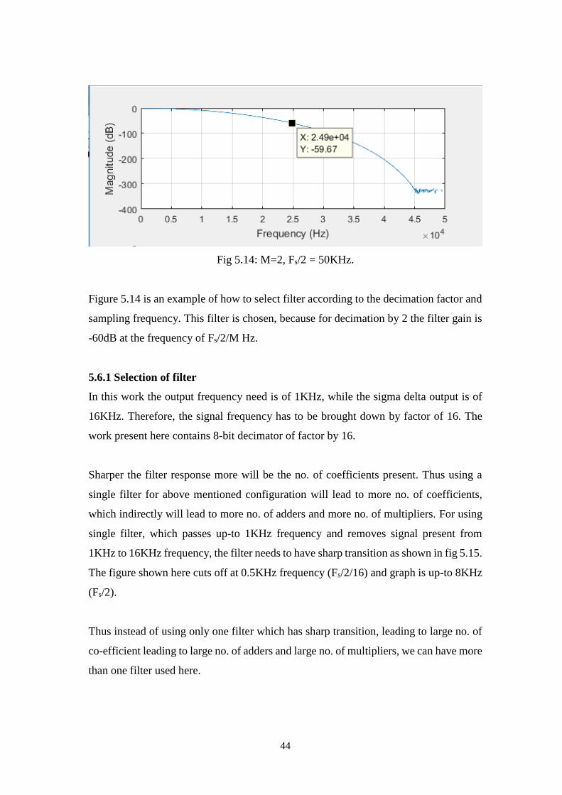
Fig 5.14: M=2, Fs/2 = 50KHz.
Figure 5.14 is an example of how to select filter according to the decimation factor and
sampling frequency. This filter is chosen, because for decimation by 2 the filter gain is
-60dB at the frequency of Fs/2/M Hz.
5.6.1 Selection of filter
In this work the output frequency need is of 1KHz, while the sigma delta output is of
16KHz. Therefore, the signal frequency has to be brought down by factor of 16. The
work present here contains 8-bit decimator of factor by 16.
Sharper the filter response more will be the no. of coefficients present. Thus using a
single filter for above mentioned configuration will lead to more no. of coefficients,
which indirectly will lead to more no. of adders and more no. of multipliers. For using
single filter, which passes up-to 1KHz frequency and removes signal present from
1KHz to 16KHz frequency, the filter needs to have sharp transition as shown in fig 5.15.
The figure shown here cuts off at 0.5KHz frequency (Fs/2/16) and graph is up-to 8KHz
(Fs/2).
Thus instead of using only one filter which has sharp transition, leading to large no. of
co-efficient leading to large no. of adders and large no. of multipliers, we can have more
than one filter used here.

45
Fig 5.15: Single filter, cut-off 0.5KHz and Fs = 16KHz.
Now in place of single filter with sharp cut-off frequency, we design more no. of filters
with less sharpness in cut-off frequency, we get less no of co-efficient.
Sinc filter is one of the filter which doesn’t have transition has sharp as shown in fig
5.15. An example of sinc filter is shown in fig 5.14. Sinc filter will have less no. of co-
efficient compare to filter shown in fig 5.15.
But using only single sinc filter such that -60Db point is reached at 0.5KHz will decrease
the no. of co-efficient but not much to a greater extend.
Thus using multiple filters with cut-off present at the intermediate value and using sinc
filter will decrease the no. of co-efficient. Now intermediate filter used here can also
have a decimation factor as shown in fig 5.7. While whole block of it can be shown in
fig 5.16. that is after each filter there can be decimation.
Filter1 M1
2* fm * OSR 2 * fm÷ OSR
Filter-n Mn
Fig 5.16: Block Diagram of decimator used in this work.

46
Now deciding the no. of filters and with respect to each filter the decimation factor is
the task here. While some filters may not have corresponding decimation factor to it. It
is used only for filtering out the high frequency unwanted signal.
There is no proper formula for deciding the no. of filters needed depending on the
decimation factor. It’s a trial and error method used here. Thus the result obtained from
this method is shown in Table 5.1
Filter
Coefficients
Decimation factor
FIR (8K – 0.5K)
200
16
Sinc (8K – 4K) + FIR (4K – 0.5)
22+100
2 * 8
Sinc (8K – 4K) + Sinc (4K – 2K)
+
FIR (2K – 0.5K)
22 + 22 + 52
2 * 2 * 4
Sinc (8K – 5.3) + Sinc (5.3K –
3.5K) + Sinc (3.5 - 2.1K) + FIR
(2K – 0.5K)
12+12+12+52
1 * 2 * 2 * 4
Table 5.1: Result of various filter used for decimation factor of 16.
* Sinc (8K – 4K) == Sinc ( fs / 2 - (-60dB pt)).
As can be seen from table 5.1 the best result in terms of no. of co-efficient is from the
result four, were three sinc filters are used along with one basic Fir filter. Each sinc filter
has 12 co-efficient used here while FIR filter has 52 co-efficient thus total no. of co-
efficient used in this case 88.
This number is very much less result which is shown in top of table were only one FIR
filter is used.

47
The first filter used here does not have corresponding decimation factor to it, its only
used for filtering out the high frequencies unwanted signals.
5.7 Design in Simulink and in Verilog.
The above mentioned process was done in Matlab, while for hardware application that
is to check frequency response curve of the above mentioned can only be obtained after
passing the signal to hardware blocks of matlab.
Simulink helps in implementing these hardware blocks in matlab. These blocks doesn’t
generate any physical blocks, but to check the result from matlab this tool is used. In
Simulink poly-phase architecture is implemented for all the filters.
With the help of Simulink and matlab the length of the co-efficient is decided.
The exact value of these co-efficient are then used in Verilog design, with the help of
these value results will be obtained.

48
Chapter 6
Results and conclusion.
6.1 Offset cancellation block result.
Case 1: If Rref > R, Iref =1uA, then the result obtained is shown in fig 6.1. The 0.25mV
extra is obtained because of resistance offered by switch.
Difference initially is of 1mV [ (18K-17k) * 1uA] which has been decreased considerably at the end of reconfiguration
Fig 6.1

49
Case 2: If Rref < R, Iref =1uA, then the result obtained is shown in fig 6.2. The 0.25mV
extra is obtained because of resistance offered by switch.
Fig: 6.2
Conclusion of Offset cancellation Block: The extra voltege present (0.25mV) has to
be removed.
The sigma delta ADC has to be used instead of SAR ADC for high resolution of signal.
6.2 Decimator Result
The decimator was designed in both matlab and in Verilog code domain, actually the
co-efficient of filters are obtained through matlab and then used in Simulink and verilog
code.
The filter response for each filter is shown below. Here result of Simulink and matlab
is compared in picturised form.
Difference initially is of 3.43mV [ (21.43K-18k) * 1uA] which has been decreased considerably at the end of reconfiguration

50
6.2.1 First Sinc Filter Output.
Fig 6.3: Left side matlab output , right side Verilog output of 1st sinc filter.
6.2.2 Second Sinc Filter output.
Fig 6.4: Left side matlab, right side Verilog output of 2nd sinc filter.

51
6.2.3 Third Sinc filter output
Fig 6.5: Left side matlab, right side Verilog output of 3rd sinc filter.
6.2.4 FIR filter output
Fig 6.6: Left side matlab, right side Verilog output of FIR filter
The red arrow shown above represents the SNR of the signal, and it is around 50dB,
which represents 8-Bits of digital output of Sigma delta ADC.
Comparing the output with that of Verilog the only difference is of noise floor level
base. SNR in both the cases are same but the noise floor in Verilog code is less then
that of present in matlab code one.

52
References
[1] P. R. Nagarajan, B. George, and V. J. Kumar, “A linearizing digitizer for wheatstone
bridge based signal conditioning of resistive sensors,” IEEE Sensors J., vol. 17, no. 6,
pp. 1696–1705, Mar. 2017..
[2] S. Ghosh, A. Mukherjee, K. Sahoo, S. K. Sen, and A. Sarkar, “A novel sensitivity
enhancement technique employing wheatstone’s bridge for strain and temperature
measurement,” in Proc. C3IT, Hooghly, India, Feb. 2015, pp. 7–8.
[3] S. Parameswaran and N. Krishnapura, "A 100 uw decimator for a 16 bit 24 khz
bandwidth audio delta-sigma modulator," in Circuits and Systems (ISCAS), Proceedings
of 2010 IEEE International Symposium on, 2010, pp. 2410-2413
[4] M. Laddomada, "Comb-based decimation filters for sigmadelta aid converters: Novel
schemes and comparisons," IEEE Transactions on Signal Processing, vol. 55, no. 5, pp.
1769-1779, 2007.
[5] B. White and M. Elmasry, "Low-power design of decimation filters for a digital if
receiver," IEEE Transactions on Very Large Scale Integration (VLSI) Systems, vol. 8, no.
3, pp. 339-345, 2000.
[6] S. Pavan, N. Krishnapura, R. Pandarinathan, and P. Sankar, “A power optimized
continuous-time delta-sigma ADC for audio applications,” IEEE J. Solid-State Circuits,
vol. 43, no. 2, pp. 351–360, Feb. 2008
[7] Multirate filtering for digital signal processing by LIjiljana.
[8] Antonio J. Ldpez-Martin, Mike1 Zuza, Alfonso Carlosena “A CMOS INTERFACE FOR
RESISTIVE BRIDGE TRANSDUCERS” ieee 2002.
[9] A. Lhpez-Martin, M. Zuza, A. Carlosena, “A CMOS piecewise linear A/D converter for
linearizing sensor characteristics,” in hoc. ICECS, Malta, pp. 659-662, Sep. 2001
[10] C. C. Liu, S. J. Chang, G. Y. Huang and Y. Z. Lin, "A 10-bit 50-MS/s SAR ADC With a
Monotonic Capacitor Switching Procedure," in IEEE Journal of Solid-State Circuits, vol.
45, no. 4, pp. 731-740, April 2010.
[11] Pravanjan patra Kunal yadav, nagveni vamsi ., ” A 343nW Biomedical Signal Acquisition System Powered by Energy Efficient (62.8%) Power Aware RF Energy Harvesting Circuit,” in 2016 IEEE International Symposium on Circuits and Systems (ISCAS), montreal, 2016.

53
[12] Pravanjan patra Kunal yadav, nagveni vamsi ., ” A 343nW Biomedical Signal Acquisition System Powered by Energy Efficient (62.8%) Power Aware RF Energy Harvesting Circuit,” in 2016 IEEE International Symposium on Circuits and Systems (ISCAS), montreal, 2016,