a short review of state-of-the-art; dft atomistic methods
TRANSCRIPT

page 113/07/07 CIAR Summar Workshop, June 29, 2007, Part 2
Outline:
• A short review of state-of-the-art;
• DFT atomistic methods;
• The NEGF-DFT implementation;
• Applications of NEGF-DFT;
• Quantum mechanic forces during current flow;
• Summary: outlook to the near future.
page 213/07/07 CIAR Summar Workshop, June 29, 2007, Part 2
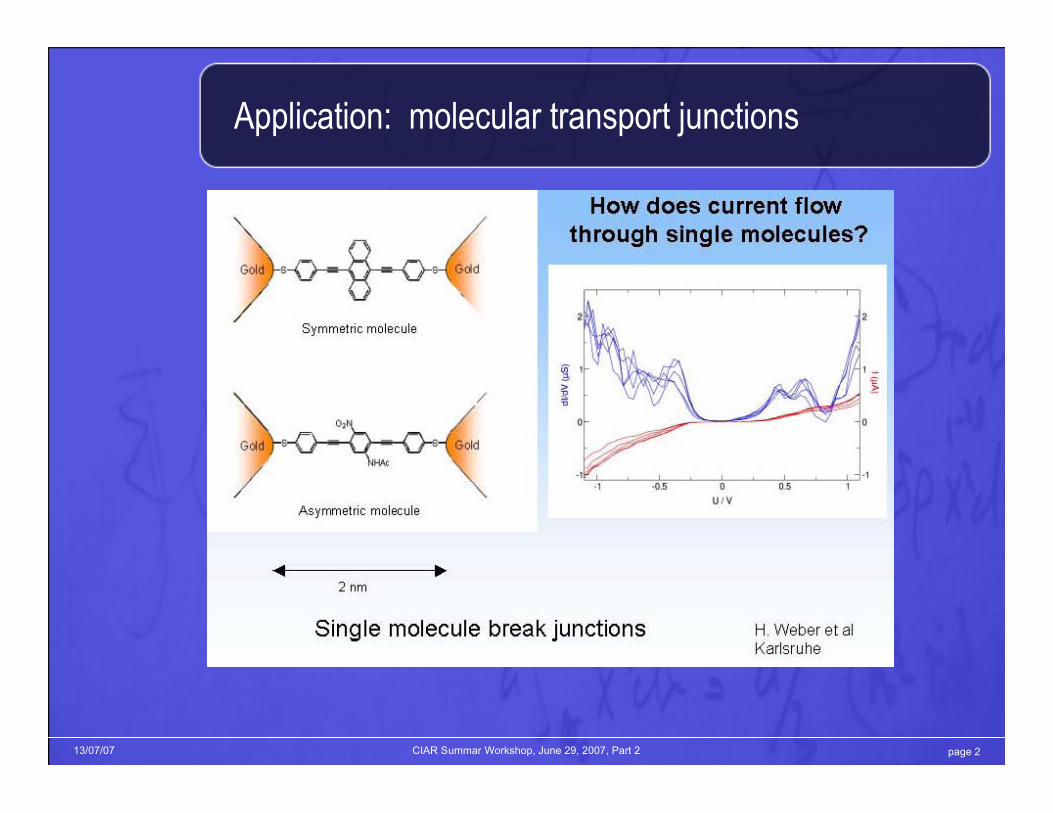
Application: molecular transport junctions

page 313/07/07 CIAR Summar Workshop, June 29, 2007, Part 2
Can we compare with experimental data? There aresome difficulties:
• Do not know experimental device structure;• Do not know environmental effects;• Do not know quality of contacts;• Do not have reliable data on single molecule device;• Do not have all the physics in our theory;• …..
But progress are being made….

page 413/07/07 CIAR Summar Workshop, June 29, 2007, Part 2
Takao Ishida etal., J. Phys. Chem. B 106, 5886 (2002)
Example: resistance of molecular wires
Slope1.76

page 513/07/07 CIAR Summar Workshop, June 29, 2007, Part 2
Another independent experiment from a different lab:David J. Wold etal. J. Phys. Chem. B, 106, 2813, (2002)
Very similar numberswere obtained as thoseof Ishida

page 613/07/07 CIAR Summar Workshop, June 29, 2007, Part 2
Our calculations:
C.C. Kaun, B. Larade and H.G, PRB (2003)

page 713/07/07 CIAR Summar Workshop, June 29, 2007, Part 2
Planar vs rotated conformations:
page 813/07/07 CIAR Summar Workshop, June 29, 2007, Part 2
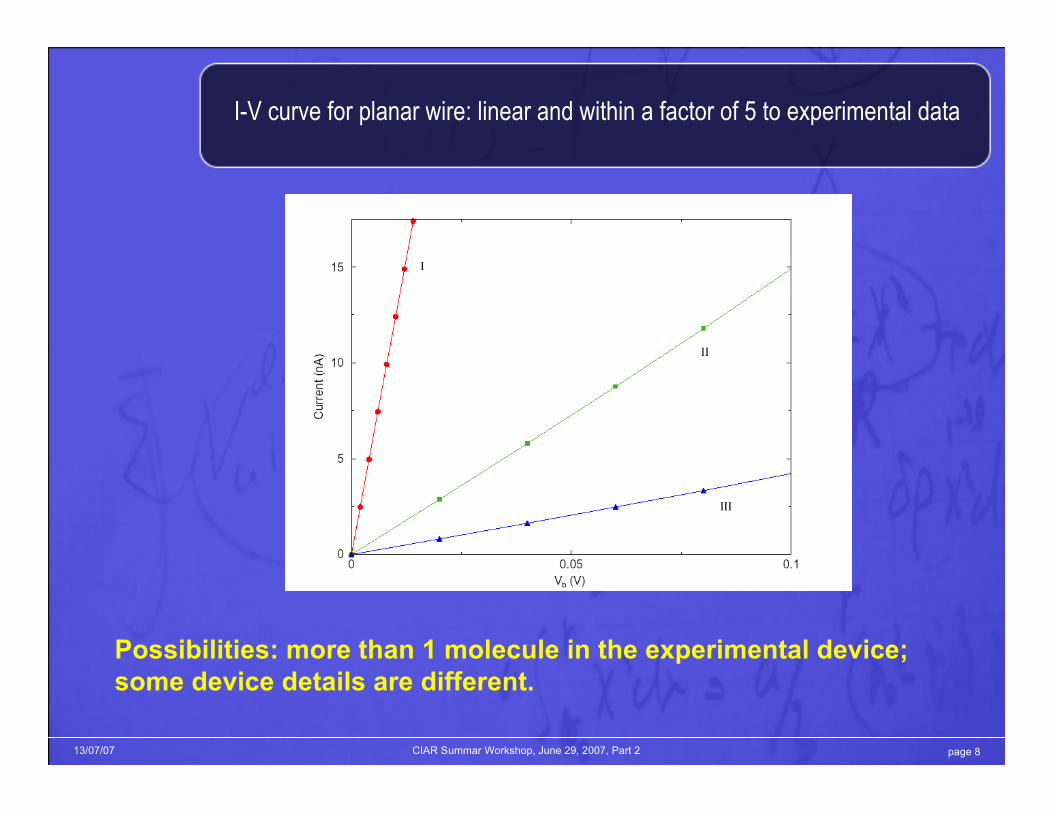
I-V curve for planar wire: linear and within a factor of 5 to experimental data
Possibilities: more than 1 molecule in the experimental device;some device details are different.

page 913/07/07 CIAR Summar Workshop, June 29, 2007, Part 2
Resistance: order of magnitude comparison can be well made
Experimentalrange:
1.7 and 2.2.
planar
rotated
The slope is independent with number of molecues

page 1013/07/07 CIAR Summar Workshop, June 29, 2007, Part 2
It is a non-resonance conduction: consistent with an exponentialincrease of resistance.
page 1113/07/07 CIAR Summar Workshop, June 29, 2007, Part 2
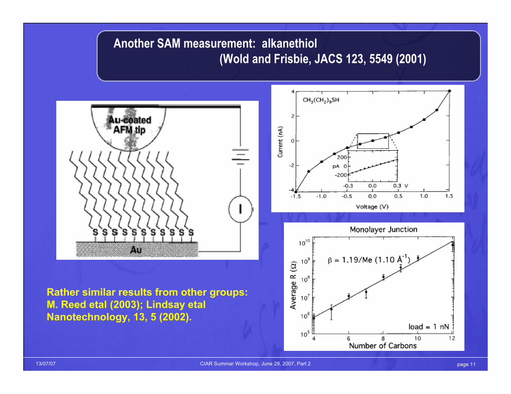
Another SAM measurement: alkanethiol (Wold and Frisbie, JACS 123, 5549 (2001)
Rather similar results from other groups:M. Reed etal (2003); Lindsay etalNanotechnology, 13, 5 (2002).
page 1213/07/07 CIAR Summar Workshop, June 29, 2007, Part 2
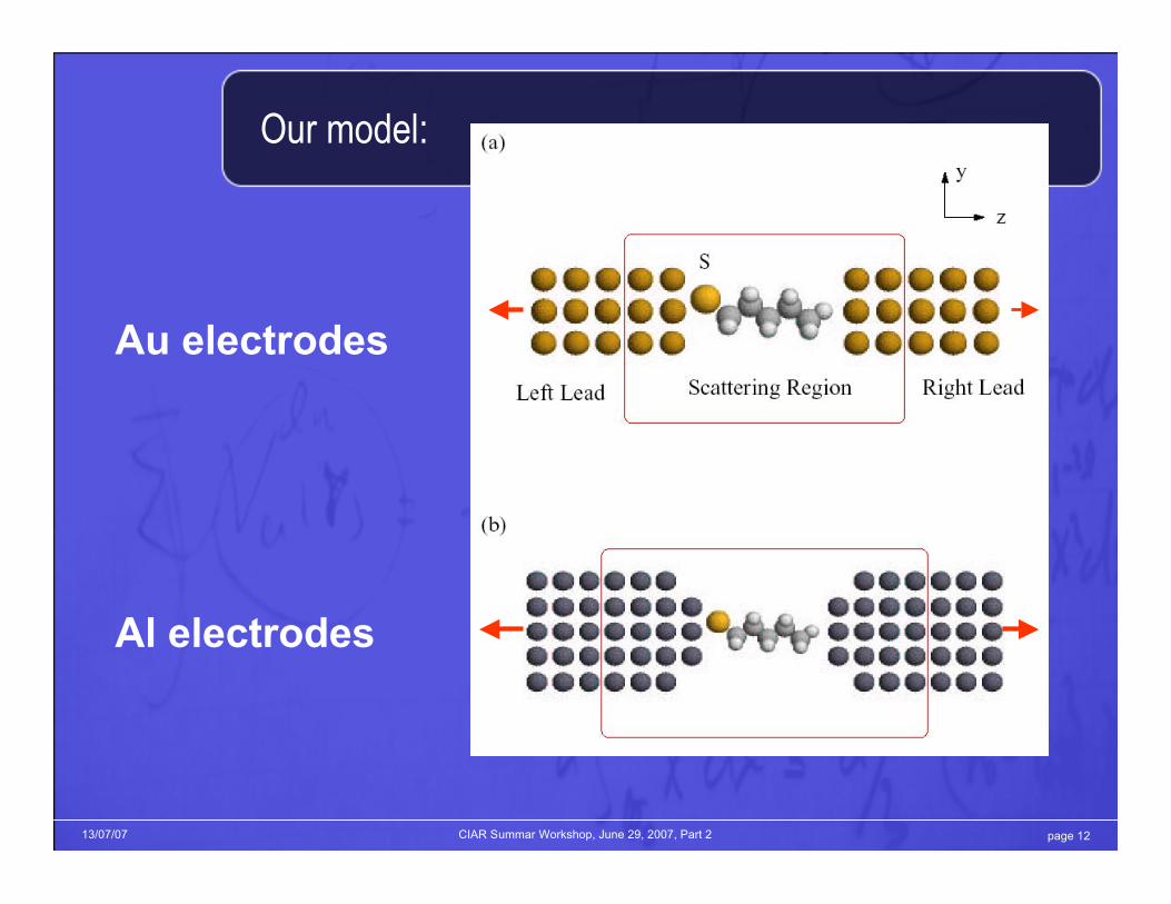
Our model:
Au electrodes
Al electrodes
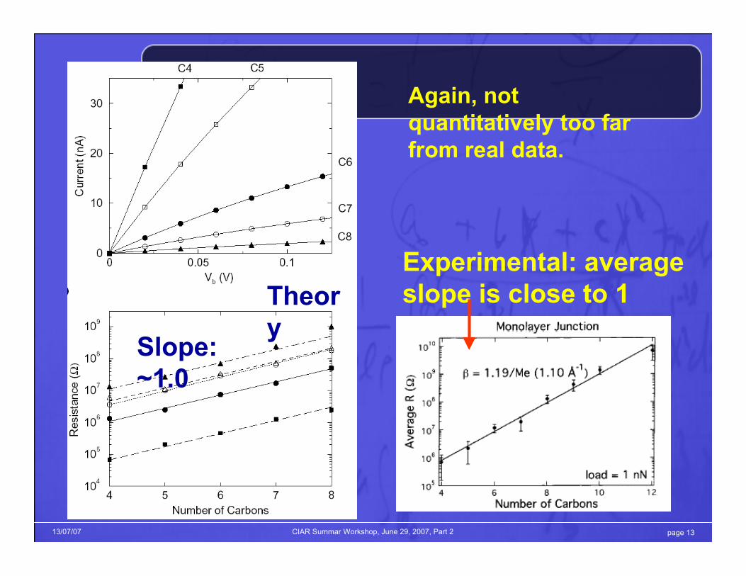
page 1313/07/07 CIAR Summar Workshop, June 29, 2007, Part 2
Experimental: averageslope is close to 1
Again, notquantitatively too farfrom real data.
Slope:~1.0
Theory

page 1413/07/07 CIAR Summar Workshop, June 29, 2007, Part 2
Au-alkanedithiol-Au wire: S-atom on both side
• Our calculation: still ;
• Our calculated beta is still about 1.0;
• Our is smaller than that of alkanethiol by about a factor of 18.
)exp( nRRon
!=
oR
Experiments so far:
1. Cui etal, J. Chem. Phys. 106, 8069(2002):
one lead is a quantum dot
Engellkes etal (Frisbie lab) (2003):
57.0=!
05.1=!Lee and Reed, J.Phys.Chem. (2004):
(Experimental ratio: 16.1 by Lee and Reed, J.Phys. Chem. (2004))
~ 1 if QD effect istaken out
page 1513/07/07 CIAR Summar Workshop, June 29, 2007, Part 2
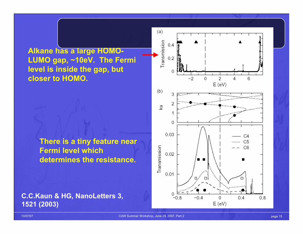
C.C.Kaun & HG, NanoLetters 3,1521 (2003)
Alkane has a large HOMO-LUMO gap, ~10eV. The Fermilevel is inside the gap, butcloser to HOMO.
There is a tiny feature nearFermi level whichdetermines the resistance.

page 1613/07/07 CIAR Summar Workshop, June 29, 2007, Part 2
Contact: structural details matter
X. D. Cui etal, Science 294, 571 (2001). B. Xu and N. J. Tao, Science 301, 1221 (2003).
D. Wold etal. J. Phys. Chem. B, 106, 2813, (2002); T. Ishidaetal., J. Phys. Chem. B 106, 5886 (2002)
planar
rotated
While the scaling factor agrees, the value ofabsolute value of resistance differs.
)exp( nRRon
!=

page 1713/07/07 CIAR Summar Workshop, June 29, 2007, Part 2
Atomistic transport: conductance of gold-BDT junction
~0.05usDelaney etal, PRL93,36805(2004)Cluster CI + Wigner function on boundary
3-5usBauschlicher Jr. etal. Chem. Phys. Lett388,427(2004). NEGF+B3PW91 or B3LYP
~20usStokbro etal. Comput. Matter. Sci27,151(2003) . NEGF + LDA
0.85usTao etal. Nano Lett 4, 267(2003).Experiment: measures large number ofsystems and average.
0.6 – 0.9 usNing etal., PRB72, 155403(2005)NEGF+B3LYP + correction from UPSreference data
1.55usVarga etal. PRL 98,76804(2007). Closedsystem with complex boundary potential
It appears to suggestthat Fermi levelalignment is criticalfor this problem.

page 1813/07/07 CIAR Summar Workshop, June 29, 2007, Part 2
Experimental:
G = 0.0012 g
Theory:
G = 0.0023g
Statistical analysis of about1000 wires each having slightdifferent contact geometry.
Hu etal PRL 95, 156803 (2005)
Statistical analysis of many contacts:

page 1913/07/07 CIAR Summar Workshop, June 29, 2007, Part 2
Summary of molecular wire:
• A non-resonance transport controls these molecular wires.Quantitative consistency to experimental data appears tobe obtained on the exponential length scale beta.
• The values of resistance and currents are within a factor of2~30 to the measured data. The difference is likely due tothe presence of multiple molecules in the experimentaljunction, details of contacts, etc.
• Encouraging but further quantitative work are needed.

page 2013/07/07 CIAR Summar Workshop, June 29, 2007, Part 2
Application: magnetic tunnel junctions
Picture from J. Akerman, Science,308, 508 (2005).
Memory used in digital devices: S-RAM; D-RAM; Flash; …
We desire an “universal memory”.
Picture from W. Butler, Nature Mat., 3, 845(2004).
MRAM

page 2113/07/07 CIAR Summar Workshop, June 29, 2007, Part 2
The hope for magnetic logic:
Picture from the experimentalproposal of programmablemagnetic logic cell based onMTJ, A. Ney etal. Natture 425,p485 (2005).
A+B switches M1; A+B+C switches M2. By manipulating with thesecurrents, Ney showed logic operations of AND, OR, etc.

page 2213/07/07 CIAR Summar Workshop, June 29, 2007, Part 2
Metal spintronics: magnetic tunnel junctions (MTJ)
!!""
""+ NNNNI
tot~
!"!!
!""!
!"
#
+
tottot
tot
II
NNNNI ~
Picture from Zutic etal Rev. Mod. Phys. 76, 323 (2004).
upup up down
up-up:
up-down:
Prinz, Science, 282, 1660 (1998)
Julliere, Phys.Lett. A 54, 225(1975)

page 2313/07/07 CIAR Summar Workshop, June 29, 2007, Part 2
Metal spintronics: Fe/MgO/Fe MTJ
Picture from M. Coey, NatureMat. 4, 9(2005).
• Rapid progress on TMRratio in recent yearsdue to progress inmaterials science
page 2413/07/07 CIAR Summar Workshop, June 29, 2007, Part 2
Device merits for applications:
• The greater the TMR, the more sensitive the device. The value ofTMR appears to sensitively depend on the tunnelling structure.Theory predicted very large TMR for MgO based junctions. Thereis a need to understand these materials issues.
• The smaller the junction, the more devices can be packed per unitarea. There is a need to understand tiny junctions made ofmolecules, clusters, etc.
• All of these requires calculation schemes which take into accountmaterial and chemical details of the device structure. Most desiredis atomic based methods.

page 2513/07/07 CIAR Summar Workshop, June 29, 2007, Part 2
Fe-MgO-Fe magnetic tunnel junctions:
Yuasa et al., Nature Mat. Vol.3, 868 (2004).
180% -247%

page 2613/07/07 CIAR Summar Workshop, June 29, 2007, Part 2
When the tunnel barrier is a molecule: molecular spintronics
K. Tsukagoshi, B.W. Alphenaar and H. Ago, Nature, 401, 572 (1999).
!!
!!!"#
$%R
RRR ~ 10 %
Carbon nanotube TMR:

page 2713/07/07 CIAR Summar Workshop, June 29, 2007, Part 2
Molecular spintronics: organic semiconductors
Xiong etal Nature, 427, p821 (2004).
TMR decreases from ~10% dueto bias voltage with a scale ofroughly 0.2V.

page 2813/07/07 CIAR Summar Workshop, June 29, 2007, Part 2
Molecular spintronics: alkane-thiols
TMR decreases from ~12% dueto bias voltage with a scale ofroughly 0.01V.
Ralph etal, PRL 93, 136601 (2004)

page 2913/07/07 CIAR Summar Workshop, June 29, 2007, Part 2
Fe/MgO/Fe MTJ: Two puzzles
• Zero bias TMR ratio:• Theory: many thousands percent.• Experiment: several hundred percent.
• TMR versus bias voltage:• Theory: either increase with bias, or no dependence.• Experiment: reduce with bias.
Can we understand these things?D. Waldron etal, PRL, 97, 226802 (2006).

page 3013/07/07 CIAR Summar Workshop, June 29, 2007, Part 2
Careful check of basis functions:
It is crucial to have accurate LCAO basis sets.
badgood

page 3113/07/07 CIAR Summar Workshop, June 29, 2007, Part 2
Careful check of k-sampling:
• Due to resonancestates on surfaces ofFe, huge number of k-sample must be done.These resonancestates give “hot spots”.

page 3213/07/07 CIAR Summar Workshop, June 29, 2007, Part 2
5 layer MgO:
5-layer MgO, measured by Wulfhekel etal APL 78, p509 (2001). STM-MgO-Fe
PC
APC
!"
!"!!#
=tot
tottot
I
IITMR
Yuasa et al., Nature Mat. Vol.3, 868 (2004).
page 3313/07/07 CIAR Summar Workshop, June 29, 2007, Part 2
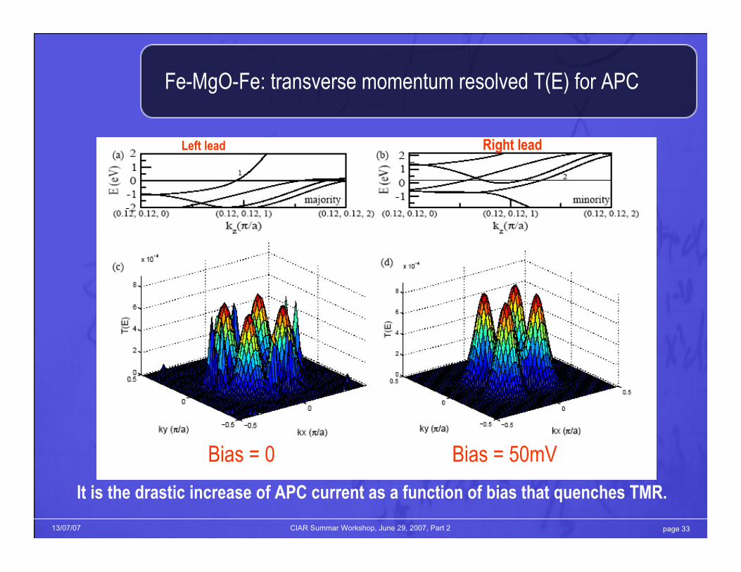
Fe-MgO-Fe: transverse momentum resolved T(E) for APC
Bias = 0 Bias = 50mV
Left lead Right lead
It is the drastic increase of APC current as a function of bias that quenches TMR.

page 3413/07/07 CIAR Summar Workshop, June 29, 2007, Part 2
Zero bias TMR: effects of small structure changes
Randomly changeinterface bonds by ~1%.
Also, randomly change all bonds by ~1%.
These small structure changes do vary the value of TMR, but not enoughto reduce it to the current experimental level (250%).

page 3513/07/07 CIAR Summar Workshop, June 29, 2007, Part 2
The remaining puzzle: zero bias TMR too large
Experimental data of Yuasa etal: ~200% (room T); Ohno etal: ~800% (5K);
Theoretical results: ~3700%.
Possible reason: oxidizationlayer exists at the Fe/MgO interfaces.
100% oxidization: TMRdropped to 169%. 50%oxidization: TMR dropped to1040%.
Experimental structure: 60%oxidization (Meyerheim etal,PRL 87, 076102 (2001).
Results:
D. Waldron etal, PRL, 97, 226802 (2006).

page 3613/07/07 CIAR Summar Workshop, June 29, 2007, Part 2
How to switch the device from PC to APC ?
J. Akerman, Science, 308, p508 (2005).• This is rather difficult
to do from fabricationpoint of view.

page 3713/07/07 CIAR Summar Workshop, June 29, 2007, Part 2
The phenomenon of spin transfer torque (STT):
STT is the torque exerted on the magnetization by spin polarized electriccurrent. It has important implications on MRAM technology.
Spin currentprecession
Co Cu Co Cu
P. Haney etal., (2007).

page 3813/07/07 CIAR Summar Workshop, June 29, 2007, Part 2
Spin Transfer Torque Haney etal (2007)
The angular pre-factor of STT has been measured experimentally in PRL84, 3149(2000). The calculated value is within a factor of 3 if assuming bulkCo damping factor, and agrees almost perfectly if assuming a reasonablevalue of thin film damping factor.

page 3913/07/07 CIAR Summar Workshop, June 29, 2007, Part 2
Summary of Fe-MgO-Fe:
• Zero bias TMR: if there is a layer of FeO between the Fe and theMgO, the TMR value is drastically reduced. For 50% oxidization,TMR=1070%.
• Large TMR is due to small APC current. A finite bias increases APCcurrent much faster than increasing PC current, causing TMR todrop.
• All voltage scales are consistent with experimental data.
• Remaining: how to reduce critical current for spin transfer torque?
page 4013/07/07 CIAR Summar Workshop, June 29, 2007, Part 2
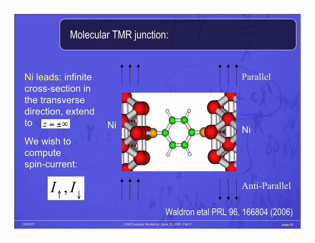
Molecular TMR junction:
±!=z
Parallel
Anti-Parallel
Ni Ni
Ni leads: infinitecross-section inthe transversedirection, extendto
We wish tocomputespin-current:
!"II ,
Waldron etal PRL 96, 166804 (2006)
page 4113/07/07 CIAR Summar Workshop, June 29, 2007, Part 2
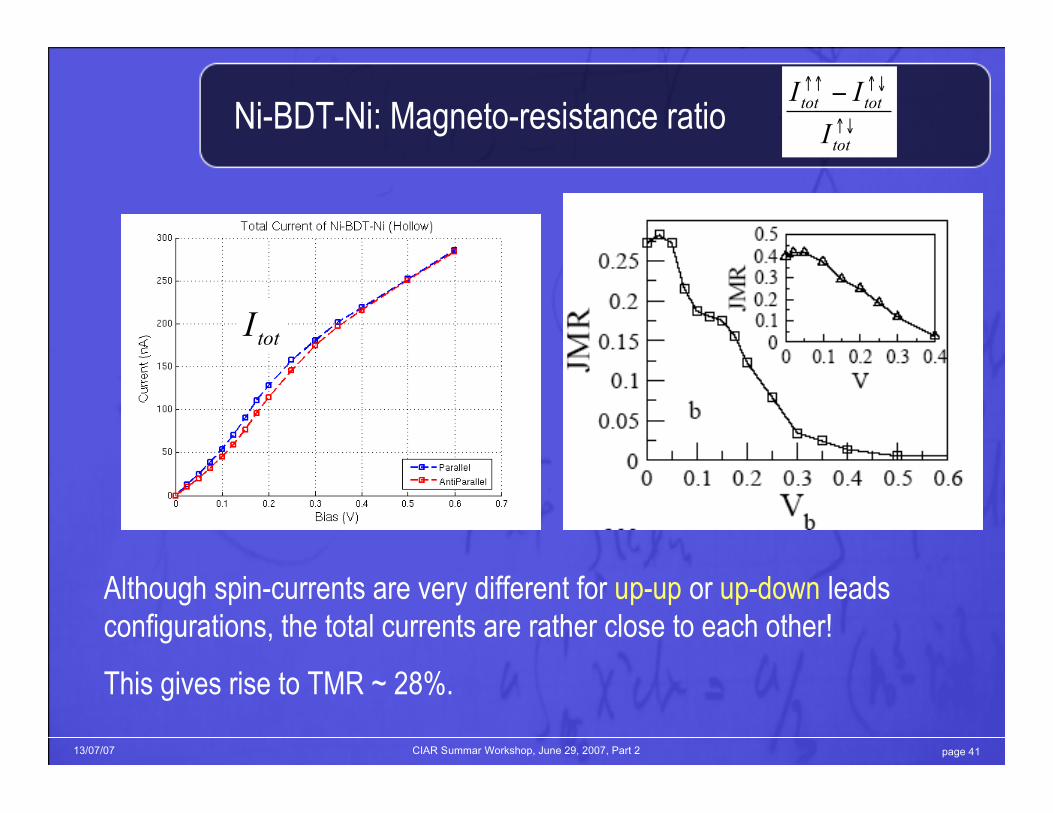
Ni-BDT-Ni: Magneto-resistance ratio
totI
Although spin-currents are very different for up-up or up-down leadsconfigurations, the total currents are rather close to each other!
This gives rise to TMR ~ 28%.
!"
!"!!#
tot
tottot
I
II
page 4213/07/07 CIAR Summar Workshop, June 29, 2007, Part 2
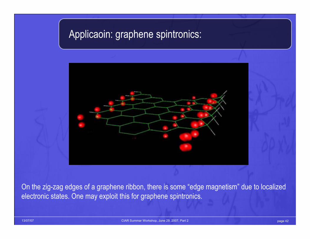
Applicaoin: graphene spintronics:
On the zig-zag edges of a graphene ribbon, there is some “edge magnetism” due to localizedelectronic states. One may exploit this for graphene spintronics.

page 4313/07/07 CIAR Summar Workshop, June 29, 2007, Part 2
Graphene can now be produced experimentally
Novoselov etal Science, 306, 666 (2004); Zhang etal Nature, 438, 201 (2005).
Single layer graphene Mobility: 2.5m2/V has been reported !

page 4413/07/07 CIAR Summar Workshop, June 29, 2007, Part 2
Transport theory for bulk graphene sheets:
For charged impurity scattering V(r), Boltzmann theory gives transportproperties. The massless fermion theory works near the Dirac point.

page 4513/07/07 CIAR Summar Workshop, June 29, 2007, Part 2
Son, Cohen and Louie, Nature (2006).
Zig-zag along y-axis(transport direction).
Electric field along x-axis,shifting spin resolved DOSrelative to the Fermi level,producing a half-metallicbehaviour.
Beautiful descriptions of zigzag graphene nano-ribbons (ZGNR).

page 4613/07/07 CIAR Summar Workshop, June 29, 2007, Part 2
“Edge” states from DFT-LDA:
Miyamoto etal PRB 59, 9858 (1999).
page 4713/07/07 CIAR Summar Workshop, June 29, 2007, Part 2
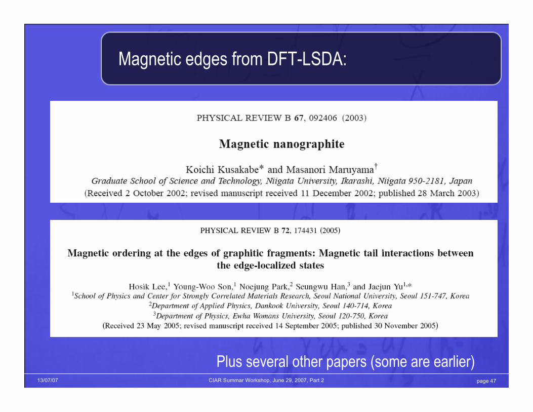
Magnetic edges from DFT-LSDA:
Plus several other papers (some are earlier)

page 4813/07/07 CIAR Summar Workshop, June 29, 2007, Part 2
Dangling bonds and edge states:
V. Timochevski (2006)
LAPW calculation by WIEN2K.
Lee etal, PRB 72 (2005)

page 4913/07/07 CIAR Summar Workshop, June 29, 2007, Part 2
Magnetic moment per atom for pure ribbon:
page 5013/07/07 CIAR Summar Workshop, June 29, 2007, Part 2
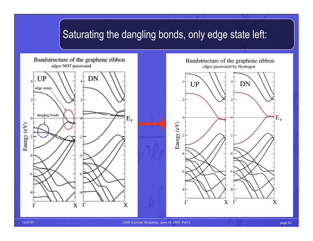
Saturating the dangling bonds, only edge state left:

page 5113/07/07 CIAR Summar Workshop, June 29, 2007, Part 2
H-graphene-H2
page 5213/07/07 CIAR Summar Workshop, June 29, 2007, Part 2
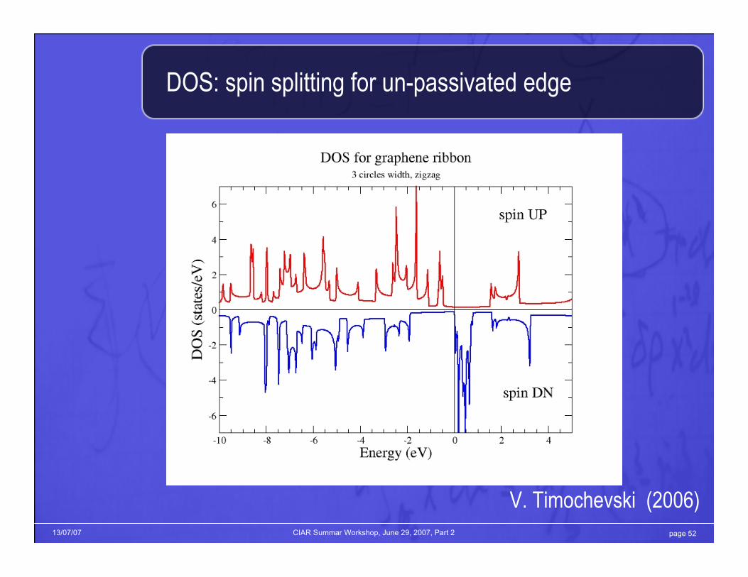
DOS: spin splitting for un-passivated edge
V. Timochevski (2006)

page 5313/07/07 CIAR Summar Workshop, June 29, 2007, Part 2
DOS: spin splitting for H-passivated edge
V. Timochevski (2006)

page 5413/07/07 CIAR Summar Workshop, June 29, 2007, Part 2
H-graphene-H2
V. Timochevski (2006)
page 5513/07/07 CIAR Summar Workshop, June 29, 2007, Part 2
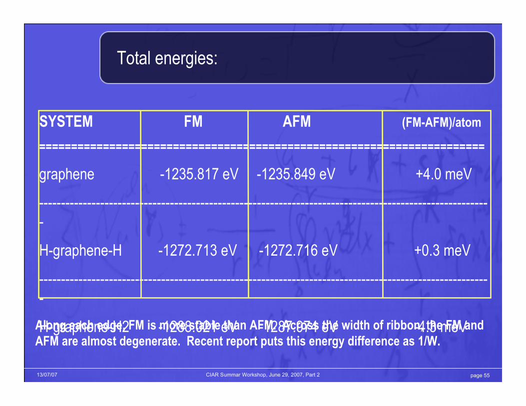
Total energies:
SYSTEM FM AFM (FM-AFM)/atom
======================================================================
graphene -1235.817 eV -1235.849 eV +4.0 meV
--------------------------------------------------------------------------------------------------------
H-graphene-H -1272.713 eV -1272.716 eV +0.3 meV
--------------------------------------------------------------------------------------------------------
H-graphene-H2 -1288.021 eV -1287.974 eV -4.3 meVAlong each edge, FM is more stable than AFM. Across the width of ribbon, the FM andAFM are almost degenerate. Recent report puts this energy difference as 1/W.

page 5613/07/07 CIAR Summar Workshop, June 29, 2007, Part 2
More Accurate Calculations?
The accuracy depends on the level of theory: but there arealways some approximations in theory.
Magnetic Measurement?
Magnetic measurements, e.g surface magnetic opticalKerr effect (SMOKE) and/or electron cycle resonance(ECR) cannot provide spatial resolution down to theatomic scale.
Real SpaceObservations?
Real space local probe by spin polarized STM may bepossible. Does the edge magnetism give enough spincontrast in STM?
Simulation of STM spin contrast (Wei Ji etal, (2007)).
Are these correct ? Can one measure them ?
page 5713/07/07 CIAR Summar Workshop, June 29, 2007, Part 2
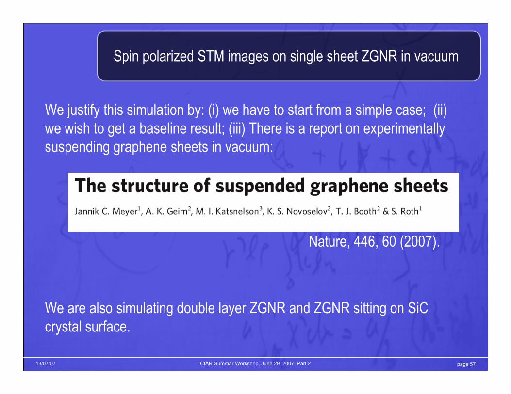
Spin polarized STM images on single sheet ZGNR in vacuum
We justify this simulation by: (i) we have to start from a simple case; (ii)we wish to get a baseline result; (iii) There is a report on experimentallysuspending graphene sheets in vacuum:
Nature, 446, 60 (2007).
We are also simulating double layer ZGNR and ZGNR sitting on SiCcrystal surface.
page 5813/07/07 CIAR Summar Workshop, June 29, 2007, Part 2
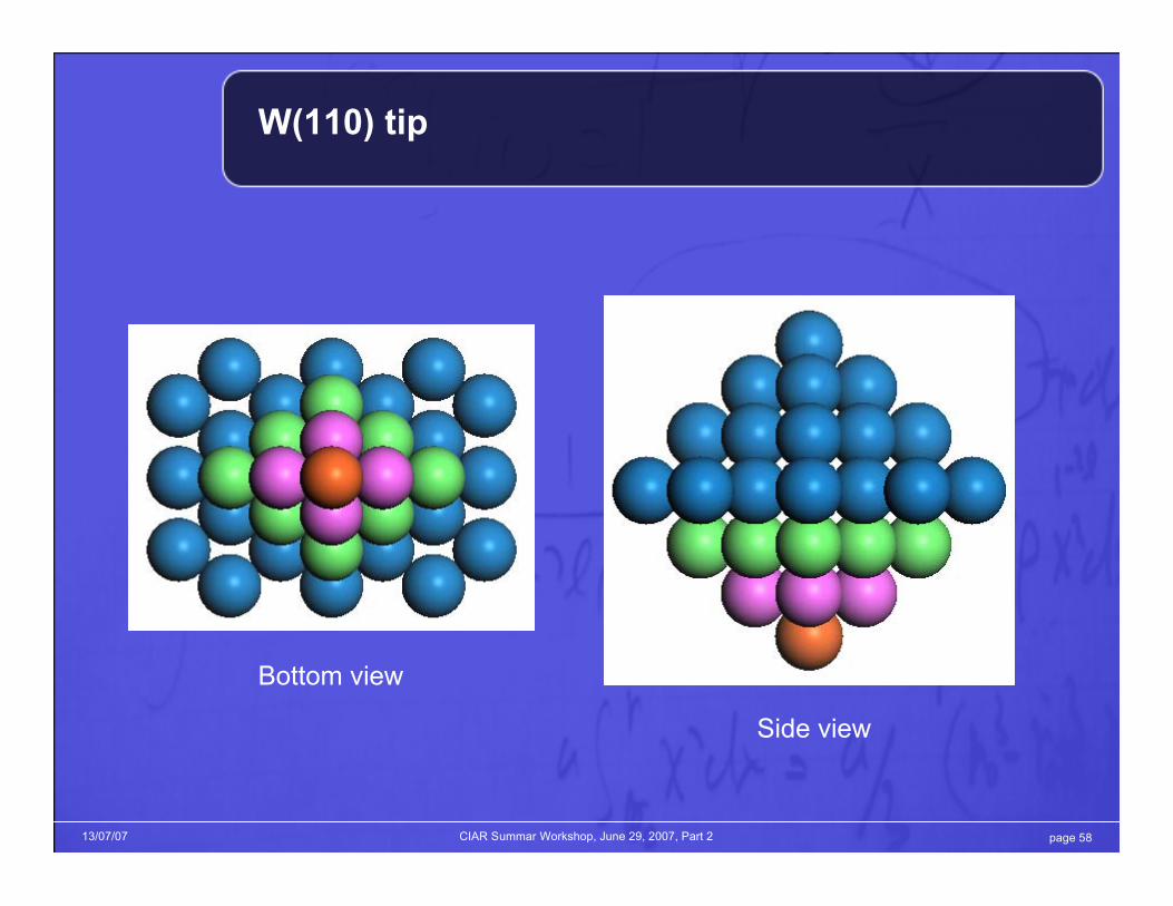
W(110) tip
Bottom view
Side view

page 5913/07/07 CIAR Summar Workshop, June 29, 2007, Part 2
W(110)-Cr tip
Bottom view
Side view
W
Cr

page 6013/07/07 CIAR Summar Workshop, June 29, 2007, Part 2
Simulation 1- spin polarized edge with W tipUnitcell
-1 0 1
-0.4
-0.2
0.0
0.2
0.4
DO
S
Energy
-0.32 eV -0.20 eV
-0.10 eV
0.30 eV0.10 eV
0.45 eV
Interesting Levels:-0.32 eV,-0.20 eV,-0.10 eV,+0.10 eV,+0.30 eV,+0.45 eV,
Two contrasts:-0.80 eV+0.80 eV
+0.80 V+0.45 V+0.3 V+0.1 V-0.10V-0.20 V-0.32 V-0.80 V
Spin non-resolvedW110 Tip
I: 40 pA
Spin is not resolved.
VASP+BSKAN, Hofer(2003).

page 6113/07/07 CIAR Summar Workshop, June 29, 2007, Part 2
-0.21
32
+0.1 +0.2
Spin non-polarized edgeSpin polarized edge
Simulation 2- spin non-polarized edge with W & Cr tips
-0.2 -0.1-0.2
30
1+0.1 +0.2
Spin non-resolved tip Spin resolved tip Spin non-resolved tip

page 6213/07/07 CIAR Summar Workshop, June 29, 2007, Part 2
Simulation 3 - spin polarized edge with Cr tip
•Spin resolved Cr tip on W(110) base•Bias Voltage: +0.1 V (Largest contrast among all interesting voltages)•Tunneling Current: 40 pA (typical current for molecular systems at low T)•Sample-tip Coupling: from FM to AFM (non-collinear spin polarization)
00˚ 180 ˚135 ˚90˚45˚Sample:
Tip:
Phi:
•Contrast reversalbetween FM and AFMcoupling only occurs atedges•The spin (non)-polarized edge statescan be resolved bychanging of tippolarizations.•Features in the outside of edges
31
11??

page 6313/07/07 CIAR Summar Workshop, June 29, 2007, Part 2
3.5
3.7
3.9
4.1
4.3
4.5
4.7
4.9
Along y direction
Height (Ang)
+0.1 V 2 pA
AFM
FM
Corrugation height of spin-polarized image
This height difference should be resolvable.

page 6413/07/07 CIAR Summar Workshop, June 29, 2007, Part 2
Summary of single layer ZGNB:
• There appears to be large enough spin contrast, detectableusing a good spin polarized STM in UHV at low temperature T.
• How low a T? We don’t know yet, but we are trying toestimate (Tao Ji at McGill, suggested by Allan MacDonald).
• Experimental challenge: produce stable single layer ZGNBhanging in vacuum

page 6513/07/07 CIAR Summar Workshop, June 29, 2007, Part 2
Graphene transport junction (GTJ):
Normalmetal lead
Graphene ribbon Normalmetal lead
Let’s compute spin polarized current through this transport junction.
Bin Wang etal. (2007).

page 6613/07/07 CIAR Summar Workshop, June 29, 2007, Part 2
Ribbon with width 5, length 10 rings:

page 6713/07/07 CIAR Summar Workshop, June 29, 2007, Part 2
Width 5, length 12:

page 6813/07/07 CIAR Summar Workshop, June 29, 2007, Part 2
Width 5, length 15 rings:
Features become sharper as L is increased.

page 6913/07/07 CIAR Summar Workshop, June 29, 2007, Part 2
Only one spin channel contributes to I-V:
Almost half metallic: a good spin filter.

page 7013/07/07 CIAR Summar Workshop, June 29, 2007, Part 2
Experimental situation
Melinda Y. Han etal.Preprint (2007).
The corresponding resistanceof these ribbons is 106 - 104
Ohm.

page 7113/07/07 CIAR Summar Workshop, June 29, 2007, Part 2
Summary of graphene spintronics
• DFT-LSDA predicts a magnetic edge for zigzag edged grapheneribbon at zero temperature. The exchange energy can be 1eV ormore.
• Thermal fluctuation will destroy 1d magnetism in the thermaldynamic limit. But for a nanoscale (or mesoscale) system, one maystill obtain some magnetic moment. Work needed to determine thislength scale.
• Spin polarized STM suggests enough spin contrast.
• Interesting anyway!
page 7213/07/07 CIAR Summar Workshop, June 29, 2007, Part 2
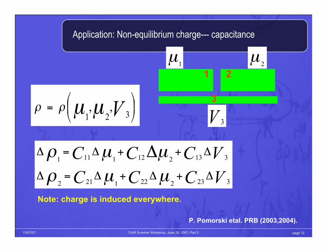
Application: Non-equilibrium charge--- capacitance
µ1
µ2
V 3
1 2
3!"
#$%
&= V 321
,,µµ''
VCCC
VCCC
3232221212
3132121111
!+!+!=!
!++!=! !
µµ"
µµ"
Note: charge is induced everywhere.
P. Pomorski etal. PRB (2003,2004).

page 7313/07/07 CIAR Summar Workshop, June 29, 2007, Part 2
aF
aF
C
C
160.0
056.0
11
21
=
!=
aF
aF
C
C
096.0
058.0
22
12
=
!=
(12,12)
(5,5)
Charging outer tube: charging innertube:
page 7413/07/07 CIAR Summar Workshop, June 29, 2007, Part 2
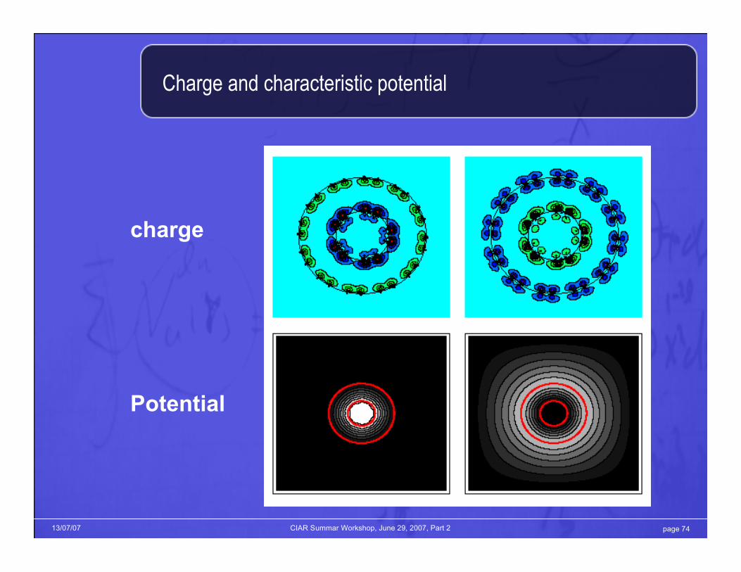
Charge and characteristic potential
charge
Potential

page 7513/07/07 CIAR Summar Workshop, June 29, 2007, Part 2
Capacitance as the two tubes approaching each other
(12,12)-(5,5) nanotube junction
C21 per unit length atlarge penetration is0.012aF.
For (5,5)-in-(12,12)periodic two-wallsystem:C21=0.014aF.

page 7613/07/07 CIAR Summar Workshop, June 29, 2007, Part 2
Classical values:
)ln(
2
1
2
0
21
R
RC
L!"=
Classical capacitance formula would predict 0.14aF or more, atleast 10 times greater than quantum result --- very wrong indeed.

page 7713/07/07 CIAR Summar Workshop, June 29, 2007, Part 2
Junction with conductance gap:
(12,0) tube (6,6) tube
This is a strange junction: both tubes are metal, they contactperfectly, but conductance is zero due to wave-function mismatch.

page 7813/07/07 CIAR Summar Workshop, June 29, 2007, Part 2
(12,0)/(6,6) junction:
Rather largecapacitance---ofcourse!
page 7913/07/07 CIAR Summar Workshop, June 29, 2007, Part 2
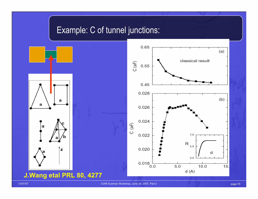
Example: C of tunnel junctions:
J.Wang etal PRL 80, 4277

page 8013/07/07 CIAR Summar Workshop, June 29, 2007, Part 2
Can we observe it ?
From WKB analysis, neglecting tunneling,Christen & Buttiker derived a formula:
qe CC
RC
11+
=
DOSC
d
AC
q
e
!
= " usual electrostatic C
quantum C due to finite DOS of plates
For C(d) to increase with d, must have 0>!
!
d
C

page 8113/07/07 CIAR Summar Workshop, June 29, 2007, Part 2
(cont.) :0>
!
!
d
C
We know where L depends
on the barrier and other system parameters, and L isusually
a few angstroms. Our analysis concludes that we can
observe the non-classical phenomena when
But
)exp(1)(L
ddR !!"
Ldd !=<*
)1(O!" for atomic plates
3104
!"#$ for macroscopic plates
page 8213/07/07 CIAR Summar Workshop, June 29, 2007, Part 2
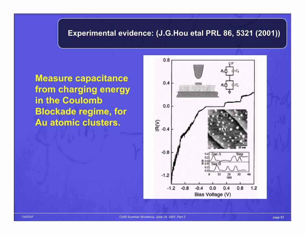
Experimental evidence: (J.G.Hou etal PRL 86, 5321 (2001))
Measure capacitancefrom charging energyin the CoulombBlockade regime, forAu atomic clusters.

page 8313/07/07 CIAR Summar Workshop, June 29, 2007, Part 2
Experiments (Hou etal PRL 86, 5321(2001)
Non-classical behavior!

page 8413/07/07 CIAR Summar Workshop, June 29, 2007, Part 2
Summary of capacitance
• Quantum corrections to non-equilibirum charge can be very important at nano-scale due to small DOS.
• Electro-chemical capacitance of molecular scale systems has non-classicalbehavior due to DOS, tunneling, bias, and DC coupling.
• By measuring C=C(V) we found a way to deduce the local density of states of ananosystem.
• Experimental work is possible, a direct dynamic measurement will be very muchdesired.