acoustic concepts in micro-scale flow control and advances
TRANSCRIPT

Acoustic Concepts in Micro-Scale Flow Controland Advances in Modular Microfluidic
Construction
by
Sean Michael Langelier
A dissertation submitted in partial fulfillmentof the requirements for the degree of
Doctor of Philosophy(Chemical Engineering)
in The University of Michigan2010
Doctoral Committee:
Professor Mark A. Burns, ChairProfessor Karl GroshProfessor Erdogan GulariProfessor Robert M. Ziff

Melancholia by Albrecht Durer

c© Sean Michael Langelier 2010
All Rights Reserved

for my parents
ii

ACKNOWLEDGEMENTS
There is simply too much to say here, but I would be remiss if I didn’t at least
try. I must first acknowledge my parents, Kathleen Mary McQuilkin and Kenneth
Paul Langelier, whose unending love and support and sacrifice figures so heavily in
the completion of this dissertation. I must also acknowledge Dan Brown. My passion
for music, which gives me so much joy and escape, is in large part his doing. I wish to
express my deepest gratitude to all of my wonderful friends and family — you know
who you are — whose kindness, patience, and character continue to provide meaning
and perspective in my life. Lastly, I want to give special thanks my dissertation
advisor Prof. Mark A. Burns whose imprimatur of scholarship, class, and guidance
have been my privilege to receive these five years.
iii

TABLE OF CONTENTS
DEDICATION . . . . . . . . . . . . . . . . . . . . . . . . . . . . . . . . . . ii
ACKNOWLEDGEMENTS . . . . . . . . . . . . . . . . . . . . . . . . . . iii
LIST OF FIGURES . . . . . . . . . . . . . . . . . . . . . . . . . . . . . . . vii
ABSTRACT . . . . . . . . . . . . . . . . . . . . . . . . . . . . . . . . . . . xiii
CHAPTER
I. INTRODUCTION . . . . . . . . . . . . . . . . . . . . . . . . . . . 1
1.1 Motivation . . . . . . . . . . . . . . . . . . . . . . . . . . . . 11.2 Mechanisms of Micro-Scale Flow Control . . . . . . . . . . . 21.3 Trends in Microfluidic Device Construction . . . . . . . . . . 41.4 Organization of this Dissertation . . . . . . . . . . . . . . . . 4
II. ACOUSTICALLY-DRIVEN PROGRAMMABLE LIQUID MO-TION USING RESONANCE CAVITIES . . . . . . . . . . . . 7
2.1 Introduction . . . . . . . . . . . . . . . . . . . . . . . . . . . 72.2 Results and Discussion . . . . . . . . . . . . . . . . . . . . . . 9
2.2.1 Acoustic Resonance . . . . . . . . . . . . . . . . . . 112.2.2 Rectification . . . . . . . . . . . . . . . . . . . . . . 132.2.3 Acoustically-Driven Liquid Motion . . . . . . . . . . 15
2.3 Materials and Methods . . . . . . . . . . . . . . . . . . . . . 192.3.1 Device Construction . . . . . . . . . . . . . . . . . . 192.3.2 Measurement of Cavity Resonance . . . . . . . . . . 202.3.3 Rectifier Flow Bias . . . . . . . . . . . . . . . . . . 202.3.4 Programmed Droplet Motion . . . . . . . . . . . . . 222.3.5 Gradient Generation . . . . . . . . . . . . . . . . . 22
2.4 Conclusions . . . . . . . . . . . . . . . . . . . . . . . . . . . . 23
iv
III. VARIED EFFECTS OF PHONONIC CRYSTAL LATTICEGEOMETRY ON THE EMERGENCE AND EVOLUTIONOF TRANSMISSION BAND GAPS . . . . . . . . . . . . . . . 24
3.1 Introduction . . . . . . . . . . . . . . . . . . . . . . . . . . . 243.2 Theory . . . . . . . . . . . . . . . . . . . . . . . . . . . . . . 263.3 Results and Discussion . . . . . . . . . . . . . . . . . . . . . . 30
3.3.1 Effects of Lattice Geometry . . . . . . . . . . . . . . 303.3.2 Analytical Modeling . . . . . . . . . . . . . . . . . . 383.3.3 Band Structure Calculations . . . . . . . . . . . . . 44
3.4 Conclusion . . . . . . . . . . . . . . . . . . . . . . . . . . . . 50
IV. ADVANCES IN MODULAR MICROFLUIDIC CONSTRUC-TION . . . . . . . . . . . . . . . . . . . . . . . . . . . . . . . . . . . 51
4.1 Introduction . . . . . . . . . . . . . . . . . . . . . . . . . . . 514.2 Materials and Methods . . . . . . . . . . . . . . . . . . . . . 53
4.2.1 SU-8 Master Mold Preparation . . . . . . . . . . . . 534.2.2 Mold Replication in Silicone . . . . . . . . . . . . . 564.2.3 Assembly Block Casting . . . . . . . . . . . . . . . 564.2.4 Substrate Preparation . . . . . . . . . . . . . . . . . 574.2.5 Device Assembly . . . . . . . . . . . . . . . . . . . . 58
4.3 Results and Discussion . . . . . . . . . . . . . . . . . . . . . . 594.3.1 SU-8 Fabrication . . . . . . . . . . . . . . . . . . . 594.3.2 Flexible Casting Trays . . . . . . . . . . . . . . . . 614.3.3 Block Design . . . . . . . . . . . . . . . . . . . . . . 624.3.4 Substrate Preparation . . . . . . . . . . . . . . . . . 654.3.5 Assembly and Bonding . . . . . . . . . . . . . . . . 67
4.4 Exemplary Applications of MAB Devices . . . . . . . . . . . 694.4.1 Chemical Gradient Synthesis . . . . . . . . . . . . . 694.4.2 Droplet Generation . . . . . . . . . . . . . . . . . . 704.4.3 Total Internal Reflectance Microscopy . . . . . . . . 72
4.5 Conclusions . . . . . . . . . . . . . . . . . . . . . . . . . . . . 74
V. CONCLUSIONS AND CONTINUING WORK . . . . . . . . 75
5.1 Conclusions . . . . . . . . . . . . . . . . . . . . . . . . . . . . 755.2 Continuing Work . . . . . . . . . . . . . . . . . . . . . . . . . 76
5.2.1 Integrated Acoustic Flow Control . . . . . . . . . . 765.2.2 Multi-Layer MABs . . . . . . . . . . . . . . . . . . 78
APPENDICES . . . . . . . . . . . . . . . . . . . . . . . . . . . . . . . . . . 81A.0.3 SU-8 Master Mold: Processing Notes . . . . . . . . 82A.0.4 Mold Replication in Silicone: Processing Notes . . . 83
v

BIBLIOGRAPHY . . . . . . . . . . . . . . . . . . . . . . . . . . . . . . . . 89
vi

LIST OF FIGURES
Figure
2.1 Resonance triggered air-flow study. (a) Conceptual representation ofthe device illustrating key components subject to the same acous-tic input. (b) Location of cavity resonance frequencies on the chro-matic scale. (c,Tone Sequence) Input acoustic signal represented bothgraphically and musically by proximity to nearest semitone on thechromatic scale. (c, bottom) Outlet flow rate as a function of timerecorded at the outlets of the four rectification structures. Output foreach resonance cavity is stable, responsive to a single musical queue,and insensitive to the presence of other competing tones. . . . . . . 10
2.2 Acoustic resonance performance of the device. (a) acoustic resonancespectrograph representing the acoustic response of each cavity (1-4) subject to a steadily ramped input frequency at constant power.Cavities 1-4 exhibit marked SWR peaks at 404 Hz, 484 Hz, 532 Hzand 654 Hz, respectively. (b) Two-dimensional incompressible flowFEM simulation result for an arbitrary cavity exhibiting resonanceat 860 Hz illustrating the effect of increased radiation losses on Q forthe aspect ratios: 2.3, 4.6, 7.7, 11.5, and 23. . . . . . . . . . . . . . 12
2.3 Rectifier outlet flow subject to ±0.03 kPa of inlet air pressure. (mainplot) Experiment showing the resulting rectifier outlet flow rate overa range of inlet pressures. (inset plot) Evolution of rectifier flow biascomputed as the difference in outlet flow rate at a given pressureswing. Bias at ±0.02 kPa represented as a pair of squared points.(inset schematic) Two-dimensional rectifier geometry used in FEMsimulations. (images at right) Velocity field snapshots from FEMtwo-dimensional incompressible flow simulations. The top two im-ages show the reversible viscous dominant flow field for extremelysmall inlet pressures ±1e-6 kPa. The bottom two images show theinertial dominant flow field at a pressure swing of ±0.01 kPa. Markeddifferences in the velocity field emerge due to flow separation and jet-ting at the rectifier inlet mouth. . . . . . . . . . . . . . . . . . . . . 14
vii

2.4 Multiplexed droplet motion. (a) Schematic representation of exper-imental setup depicting an input acoustic signal delivered to an ar-ray of resonance cavities, each of which is linked to an input on amicrofluidic device (not to scale). (b) Input acoustic signal and re-sulting droplet velocity as a function of time illustrating programmedactuation of specific droplets in response to resonant musical tonessupplied to the device. Chord amplitudes used to produce uniformdroplet velocities were: B-C (0.89, 0.85), A-D (0.76, 1.39), A-C-D(0.80, 1.18, 1.25), and A-B-C-D (0.76, 0.76, 0.90, 1.25). . . . . . . . 16
2.5 Performance of standard microfluidic unit operations using acoustically-controlled droplet motion. (top, left) schematic of branched channelPDMS device with associated cavity linkages (top, right) channel lay-out with legend illustrating the visual representation of three pres-sure states. Main pressure indicates areas where significant pressureis applied to induce droplet motion. Support pressure indicates areaswhere minimal pressure is applied to counter droplet motion. (bot-tom) Four sets of images depicting the standard fluidic unit opera-tions of merging, transport, splitting, and sorting. Arrows on eachimage indicate ensuing droplet motion in response to acoustically-generated pressures (linking image). . . . . . . . . . . . . . . . . . . 18
2.6 Acousticially-switchable gradient generation. (left) schematic repre-sentation of PDMS device used in gradient generation experiments.Resonance cavities are interfaced with the microfluidic device accord-ing to the frequencies listed. (right) A series of images depicting thestate of the tonal input (image inset schematic) and the resultingliquid gradient that is produced. Cavity pressures were all tuned to≈100 Pa. . . . . . . . . . . . . . . . . . . . . . . . . . . . . . . . . . 19
2.7 Device construction. (top) Exploded schematic view of device. (bot-tom) Detail of Cover Plate and Resonance Cavity/Recitifer with di-mensions . . . . . . . . . . . . . . . . . . . . . . . . . . . . . . . . . 21
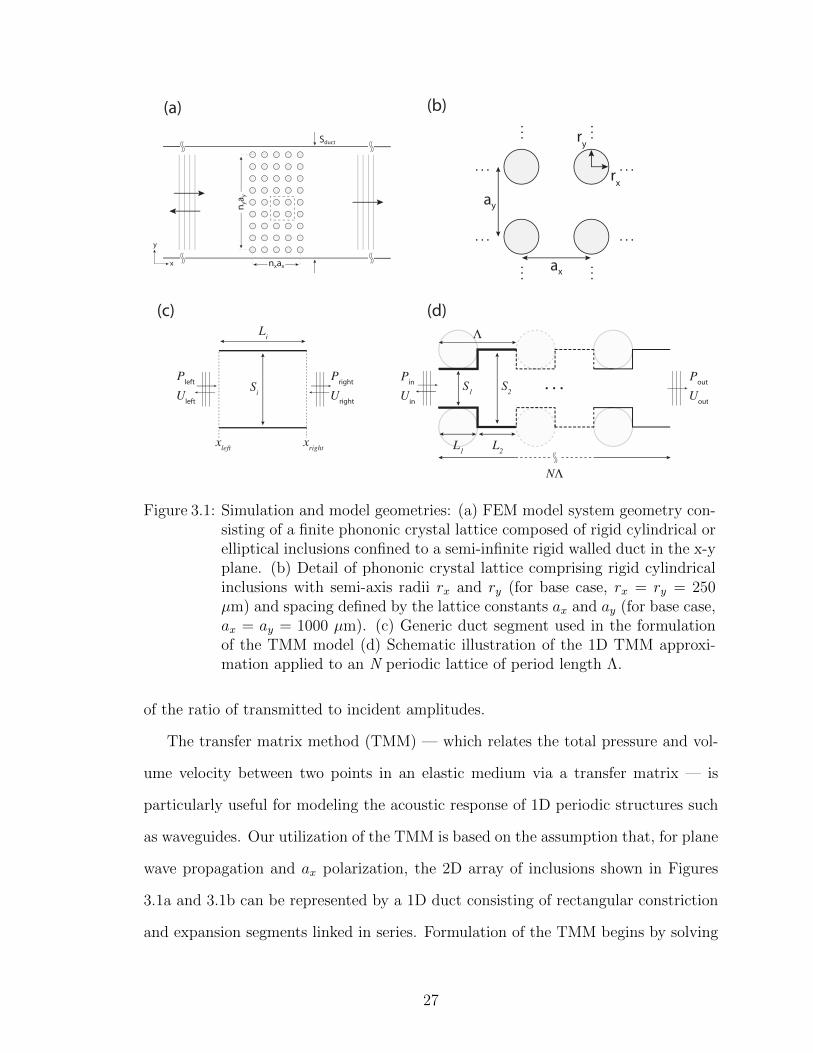
3.1 Simulation and model geometries: (a) FEM model system geometryconsisting of a finite phononic crystal lattice composed of rigid cylin-drical or elliptical inclusions confined to a semi-infinite rigid walledduct in the x-y plane. (b) Detail of phononic crystal lattice compris-ing rigid cylindrical inclusions with semi-axis radii rx and ry (for basecase, rx = ry = 250 µm) and spacing defined by the lattice constantsax and ay (for base case, ax = ay = 1000 µm). (c) Generic ductsegment used in the formulation of the TMM model (d) Schematicillustration of the 1D TMM approximation applied to an N periodiclattice of period length Λ. . . . . . . . . . . . . . . . . . . . . . . . 27
3.2 FEM transmission profiles highlighting the location and contour ofthe principal band gap (shaded regions) subject to (a) longitudinaland (b) transverse modifications to the crystal unit cell. Spacingreported relative to base lattice dimensions (outlined in bold). . . . 32
viii

3.3 FEM transmission profiles detailing the effect of inclusion x-eccentricity(insets) on the location and bandwidth of the principle band gap(shaded rectangles) as well as the break in symmetry of the massloading gap (dashed lines). . . . . . . . . . . . . . . . . . . . . . . . 34
3.4 Influence of filling fraction ratio (FF). (a) Schematics detailing thefour geometric paths taken in the modification of the FF. (b) Band-width (normalized to base case) of the principal band gap as a func-tion of FF. (c) Peak loss of the intensity transmission coefficient (nor-malized to base case) of the principal band gap as a function of FF. 36
3.5 FEM transmission profiles highlighting the rhombic transformationof the base case lattice. (a) Simulated profiles reflecting a steadyrhombic transformation of the base case lattice. (b) Schematic illus-tration of the transformation, performed by introduction of verticalshift (yshift = Φabase) between consecutive inclusion columns. (c)Pressure field images from FEM for Φ = 0 and Φ = 0.5. . . . . . . . 38
3.6 Transfer matrix (TMM) model results for crystals of varying thick-ness. (a-b) Schematic of simulated and effective 1D waveguide di-mensions used in TMM model. (c) Transmission profiles for duct-confined phononic crystals of varying thickness (left to right, nx =1, 2, 3, 5, 7, 9) as predicted by FEM (solid black curves). TMM modelresults based on simulated (dashed blue curves) waveguide dimen-sions (L1, S1, L2, S2) and effective (dashed red curves) waveguidedimensions (L1eff, S1eff, L2, S2). . . . . . . . . . . . . . . . . . . . . 40
3.7 Effective constriction dimensions relative to as simulated values. (a)longitudinal spacing relative to abase, (b) transverse spacing relativeto abase, (c) inclusion x-eccentricity relative to rbase (d) inclusion ra-dius relative to rbase. . . . . . . . . . . . . . . . . . . . . . . . . . . 41
3.8 Calculated band structure and simulated (FEM) transmission profilesfor base case crystals of varying thickness. (Center panel) Γ−X bandstructure calculated along the kx direction of the first irreducibleBrillouin zone (inset) showing the location of observed transmissiongaps (hatched rectangles) as well as the location of transverse modes(a, b, and c: pressure field images at left). (Right panel) SimulatedFEM transmission profiles of base lattice crystals (nx = 3, 5, and 9periods thick) highlighting the evolution of gap width and locationwith increasing thickness. . . . . . . . . . . . . . . . . . . . . . . . . 45
3.9 Complete pressure field mapping for the base case phononic crystaltaken from computed band structures. (Left panel) Pressure modeshapes for the first nine dispersion bands at four specific reducedwave vector locations. (Right panel) Computed Γ−X band structureof the base case phononic crystal showing the location of observedtransmission gaps as well as the location of transverse modes (dashedcurves). . . . . . . . . . . . . . . . . . . . . . . . . . . . . . . . . . 47
ix
3.10 Pressure field validation at the gap edges using nx = 5 data fromFigure 3.8. For band gaps 1-3 (left, middle, and right, respectively):pressure field images reflect FEM Simulation and Band Structureresults taken at their respective gap edges as well as the gap center(note: for band structure, no solution exists within the gap). Imagesreveal the presence of the infinite lattice modes, predicted from theband structure, in the FEM simulations. . . . . . . . . . . . . . . . 48
3.11 Complete band structure calculation of base lattice for various fillingfractions (FF). (left to right) Full band structure of base case latticealong the three high symmetry directions of the first irreducible Bril-louin zone (Γ−X−M−Γ) for FFs (obtained via isotropic scaling ofinclusion radius, r) equal to 0.13, 0.28, 0.50, and 0.64. A total bandgap is observed for filling fractions greater than 0.28. Within totalgap region wave propagation is forbidden in all directions. . . . . . . 49
4.1 The MAB concept. (a) Schematic representation of the assorted maleand female MABs used in this work (b) A selection of pre-fabricatedMABs prior to (left) and following (right) assembly and bonding. (c)Photograph of actual MAB device, of identical construction, duringa flow test. . . . . . . . . . . . . . . . . . . . . . . . . . . . . . . . . 54
4.2 SEM images of precursor SU-8 master molds. (a) Mold with ≈250µm thick walls and 80 x 200 µm fluidic channels. (b) Mold with ≈500µm thick walls and 80 x 200 µm fluidic channels. (c) Image of moldin (b) illustrating the negative pitch or sidewall irregularity that wastypically observed . . . . . . . . . . . . . . . . . . . . . . . . . . . . 58
4.3 Schematic representation of replication of SU-8 master molds in flex-ible silicone. (a) Pre-cursor master mold constructed from SU-8 ona 4” Silicon wafer. (b) Chemical surface modification of (a) withtrichlorosilanes. (c) Encapsulation of (b) with liquid silicone. (d)Positive silicone cast following release. (e) Chemical surface modifi-cation of (d) with trichlorosilanes. (f) Encapsulation of (e) with liquidsilicone. (g) Recovery of negative silicone cast following release. (h)Chemical surface modification of (g) with trichlorosilanes. (i) Fillingof MAB wells with PDMS monomer. (j) Following PDMS polymer-ization, MAB’s are released by flexure of the silicone mold. (k) Imageof actual 250 µm silicone mold during step (j). (i) Extraction of amale MAB using a pair of blunt tweezers. . . . . . . . . . . . . . . . 60
4.4 Channel alignment and offset statistics for a random sampling ofMAB junctions with various piece convexities. (a) Schematic illus-tration of a MAB junction highlighting relevant parameters: channelwidth (w), channel offset (α), channel angle (θ), piece convexity (δ).(b) Bulls-eye plot of relative channel offset (α/w) and relative chan-nel angle (θ − 180◦) for ≥ 20 MABs at each convexity. (c) Box plotof relative channel offset versus piece convexity. (d) Histogram of(c). (e) Box plot of relative channel angle versus piece convexity. (f)Histogram of (e). . . . . . . . . . . . . . . . . . . . . . . . . . . . . 63
x

4.5 Inter-block gaps for a sampling (N ≥ 20 in each case) of bondedMABs with different piece convexity. (a) Histogram of inter-blockgap magnitudes for assembled and bonded MABs of various convex-ity (four bins: 0-5 µm, 5-10 µm, 10-15 µm, and 15-20 µm). (b)Microscope image of a 0 µm gap. (c) Microscope image of a 16.7 µmgap. . . . . . . . . . . . . . . . . . . . . . . . . . . . . . . . . . . . 64
4.6 Summary of “off-the-shelf” methods for the preparation of PDMSthin-films. (a) Resulting average film thickness and variation for as-sorted preparation methods. (b) Film thickness calibration plot forpreparation using a compressed air jet (see inset). . . . . . . . . . . 66
4.7 (a) Schematic illustration of an assembled MAB device and detail(inset) of the device cross-section shown by plane No. 1 highlightingthe capillary wicking of the liquid film into the inter-block gap. (b)Companion SEM image of the cross-section defined by plane No. 1 inan actual MAB device with the same channel geometry. (c) Close-upof the highlighted rectangle in (b) showing the bond which has formedat the MAB junction well above the channel roof. (d) CompanionSEM of plane No. 2 in (a) showing the vertical bond penetrationextending from the substrate surface ≈150 µm. . . . . . . . . . . . . 68
4.8 Chemical gradient and droplet generation in MAB devices. (a) Schematicof two component chemical gradient generator constructed from 58MABs. (b) Image of completed MAB device following additionalencapsulation in PDMS. (c) Pixel intensity plot illustrating the sig-moidal variation of the generated gradient along the path M-M’ in(b). (d) Schematic of 13 block flow-focus droplet device. (e) Close-upimage of the device in (d) during operation illustrating the formationof a water droplet at the flow-focused junction (dotted lines are toillustrate channel boundaries). (f) Close-up image of the device in (d)during operation showing the generation and accumulation of highlystabilized and uniform droplets in the downstream chamber (dottedlines are to illustrate channel boundaries). . . . . . . . . . . . . . . 71
4.9 TIR Microscopy using MAB devices. (a) Simplified schematic ofobjective-based TIR microscope operation. (b) Image of 7 blockstraight channel MAB device, with attached fluidic inputs, on theTIR microscope stage. (c) Image from objective-TIR excitation ex-periment illustrating the contrast in signal strength for surface bound(bright) versus freely diffusing (dim) 200 nm nanospheres. . . . . . . 73
5.1 Candidate single cavity micro-acoustic design. Device consists of asurface mounted piezoelectric element with integrated diaphragm dis-placement and flow sensing electronics. (1) Rectifier layout similar tomacro-system. (2) Integrated bi-directional hot wire-anemometer foracoustic response characterization. (3) Surface mounted piezoelectricacoustic source. Underneath is a Helmholtz resonance cavity whichis separated from the source by a thin glass membrane. . . . . . . . 77
xi
5.2 Schematic representation of a concept multi-layer MAB device forperistaltic pumping. The device consists of a fluidic layer (bottom),a control layer (top), and a doubly-thick anchor block (gray, lowerleft) for preserving layer to layer alignment. . . . . . . . . . . . . . . 79
A.1 Current MAB photomask design. (a) Assorted simple fluidic channellayouts consisting of straight, 90 ◦ turns, T-junctions, crosses, reac-tion chambers, and inlets/outlets. Channels are drawn at 200 µmwide. Numerical indications next to the male pieces correspond tothe degree of MAB convexity in µm. (b) MAB walls for both maleand female pieces with principle block dimensions of 8 x 8 mm. . . . 84
A.2 SU-8 master mold fabrication methodology and original MAB castingtechnique. (a) SU-8 resist is spun onto a bare silicon wafer accordingto the patterns for fluidic channels and soft baked on the hot platefor 5 minutes at the 65C and for 20 minutes subsequently at the 95C.The wafer is then exposed on a contact aligner for a length of timeappropriate to the resist thickness. (b) After post-exposure baking(PEB) for 3 minutes at the 65C and for 10 minutes at the 95C, thewafer is immersed and developed in fresh SU-8 developer solution. (c)The SU-8 2150 resist is spun to a desired thickness and soft bakedfor an appropriate length of time (≈ 7 hrs for a 500 µm film. (d) Thewafer then is carefully aligned to a chrome photomask patterned withthe MAB walls exposed. (e) After the PEB, the wafer is submersiondeveloped in SU-8 developer. (f) PDMS prepolymer and curing agent(9:1 or 10:1 by weight) is cast against the mold. Then, slightly tiltthe mold and scratch the excessive PDMS solution off, using a razorblade. (g) Each cured PDMS block is carefully removed with a sharpaluminum needle. . . . . . . . . . . . . . . . . . . . . . . . . . . . . 85
A.3 Observed surface roughening of silicone replicates. (a) Microscopeimage of original SU-8 master mold following silanization treatment(20 µL trichlorosilane for 1 hr under closed vacuum). (b) Microscopeimage of replicate mold in silicone rubber following final silanizationtreatment exhibiting a slightly roughened surface topology. . . . . . 86
A.4 Variations in MAB thickness. (top) Thickness distribution of maleand female MABs taken from a 250 µm mold. (bottom) Thicknessdistribution of male and female MABs taken from a 500 µm mold. 87
A.5 Systematic variation in film thickness of prepared substrates. (mainplot) Variation in thin-film thickness as a function of location on thesubstrate (top, middle, bottom). Note: top refers to the beginning ofthe air-jet path (inset, Figure 4.6b). . . . . . . . . . . . . . . . . . . 88
xii

ABSTRACT
Acoustic Concepts in Micro-scale Flow Control and Advances in ModularMicrofluidic Construction
by
Sean Michael Langelier
Chair: Mark A. Burns
Despite thirty years of research, the full scientific and social impact of microfluidics
has not been realized. This dissertation focuses on addressing two key issues to accel-
erate this realization: micro-scale flow control and microfluidic device construction.
We introduce the design of a new acoustic-based mechanism for multiplexed pressure-
driven flow control. The device we have developed converts the frequency content of
an acoustic signal into four individually addressable pressure outputs, tunable over a
range 0-200 Pa with a control resolution of 10 Pa. The pressure generating compo-
nents of the device consist of a bank of four resonance cavities (404, 484, 532, and 654
Hz), each with an attached rectification structure. We demonstrate how this scheme
can be used for programmatic operation of both droplet-based and continuous-flow
microfluidic systems using only a single control line. We then explore an alternative
acoustic actuation scheme involving frequency dependent attenuation within finite
phononic crystals. Specifically, finite element analysis of the band properties of peri-
odic two-dimensional microstructures subject to a variety of geometric lattice pertur-
bations is presented. Phononic structures with periodicity over the range of 100-1400
xiii
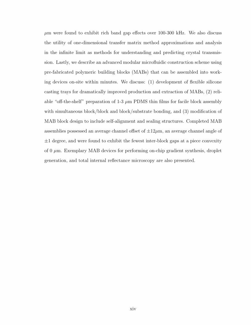
µm were found to exhibit rich band gap effects over 100-300 kHz. We also discuss
the utility of one-dimensional transfer matrix method approximations and analysis
in the infinite limit as methods for understanding and predicting crystal transmis-
sion. Lastly, we describe an advanced modular microfluidic construction scheme using
pre-fabricated polymeric building blocks (MABs) that can be assembled into work-
ing devices on-site within minutes. We discuss: (1) development of flexible silicone
casting trays for dramatically improved production and extraction of MABs, (2) reli-
able “off-the-shelf” preparation of 1-3 µm PDMS thin films for facile block assembly
with simultaneous block/block and block/substrate bonding, and (3) modification of
MAB block design to include self-alignment and sealing structures. Completed MAB
assemblies possessed an average channel offset of ±12µm, an average channel angle of
±1 degree, and were found to exhibit the fewest inter-block gaps at a piece convexity
of 0 µm. Exemplary MAB devices for performing on-chip gradient synthesis, droplet
generation, and total internal reflectance microscopy are also presented.
xiv

CHAPTER I
INTRODUCTION
1.1 Motivation
Microfluidics emerged in the late 1980s from advances in liquid chromatography.
Later, IBM — in the first major technological adaptation of micro-scale fluid physics
— developed the ink-jet print head which quickly usurped the (then dominant), dot-
matrix technology. In the years that followed, the desire for precise control of minute
(µL and pL) liquid volumes spawned innumerable applications and commercial ven-
tures, each seeking to leverage the many now broadly accepted, advantages of working
in a micro-environment (e.g., reduced reagent consumption and cost, shorter analy-
sis times, parallelization, and portability). But, even with this attention as well as
a surge in publications in the early 2000s, microfluidics remains a niche technology
falling well short of early predictions for the field.
One issue preventing the widespread adoption of microfluidic technologies relates
to the difficulties associated with micro-scale flow control. Here, the challenge is to
orchestrate the coordinated manipulation of small liquid volumes to and from various
unit operations on a microfluidic chip in order to perform a given experiment. Such a
task requires very precise control of the fluidic driving force — mechanistically, this is
typically accomplished using either pressure-driven or electrokinetic means — and is
often problematic because many of the actuation mechanisms available are not suited
1

to output the small pressure differences needed for microfluidic control. A second
issue, perhaps only relevant to academia, is that a technology gap typically exists
between the developers of microfluidic tools and end users, the majority of which
reside in the life sciences. Here, researchers who might otherwise benefit from the ap-
plication of microfluidic tools in areas such as high-throughput drug screening or cell
culture, are deterred by the high cost and expertise required to design and fabricate
custom microfluidic systems. Thus, the task(s) facing developers of microfluidic tech-
nologies — if the full impact of these tools is to be realized — is the creation of more
advanced solutions for micro-scale flow control and development of novel fabrication
strategies that facilitate use by non-experts.
1.2 Mechanisms of Micro-Scale Flow Control
Micro-scale flow control is typically accomplished using either an electrokinetic or
pressure-driven approach, each of which has its own unique set of actuation mech-
anisms, and each with its own advantages and limitations. In the electrokinetic
approach, an electric field is applied as a means of generating force on fluids and
particles [1]. Perhaps the most traditional embodiment of this mechanism is elec-
troosmotic flow (EOF). In EOF, a diffuse charge layer at the interface of a liquid
electrolyte and a dielectric migrates toward the electrode of opposite polarity and, in
the process, drags the bulk fluid along with it. The implementation of EOF is simple,
requiring only an appropriate voltage source, and to its credit, EOF has been shown
to be effective for simultaneous control of multiple fluidic inputs [2]. However, EOF
cannot be used to control gases, non-polar liquids, or discontinuous liquid phases,
and it is extremely sensitive to dielectric surface properties, impurities, and channel
layout. Electrothermal flow is also possible and arises from temperature gradients
stemming from joule heating in the working fluid [3]. This approach is rarely used,
however, as it often leads to electrochemical dissociation of the working fluid and
2
electrode corrosion.
So-called digital microfluidic systems make use of various actuation mechanisms
such as electrowetting on dielectric (EWOD) to manipulate droplets on the surface
of planar substrates which have been coated with a dielectric [4]. EWOD is advan-
tageous as it eliminates the leakage and bonding issues associated with fabricating
enclosed micro channels and is highly amenable to automation. However, EWOD
suffers from evaporation issues and is, as are all electrokinetic mechanisms, limited
to the manipulation of aqueous electrolytes.
Pressure-driven flow schemes, both passive and active, work by generating pressure
differentials within the working fluid. Passive actuation mechanisms such as capillary
pressure are unique in that they do not require external energy input in order to
function. Instead, flow in a passive system occurs spontaneously as a product of an
engineered interplay between capillary forces, surface tension, and channel geometry
[5]. Such systems, though ideal for simple unidirectional fluid transport, lack the
operational versatility necessary for complex flow control due to their deterministic
flow paths and designed dependence on specific liquid/surface properties.
Active pressure-driven mechanisms, by contrast, are extremely versatile, gener-
ally indifferent to fluid properties and channel geometry, and have the additional
benefit of being dynamically reconfigurable. The simplest active pressure generating
components, e.g. syringe pumps and pneumatics, work by direct application of exter-
nal pressure and are ideal for continuous flow applications such as particle synthesis
[6], where large stable flows are required. Reciprocating displacement mechanisms
are typically microfabricated and work by coupling the oscillatory deflection of a
diaphragm with some form of fluidic rectification structure [7, 8]. However, these sys-
tems are extremely difficult to fabricate and are prone to mechanical fatigue/failure.
Other, non-mechanical, approaches such as centrifugal force [9], and acoustic stream-
ing [10] have also been demonstrated.
3

1.3 Trends in Microfluidic Device Construction
Traditional microfabrication is performed in a clean-room environment using spe-
cialty photolithographic equipment. Unfortunately, these facilities and instruments
are extremely expensive and often require significant operational expertise, thus alien-
ating a large population of users (primarily in the life sciences) who might otherwise
benefit from the technology. In recent years, there have been numerous attempts to
lower this entry barrier by introducing fabrication pathways that minimize depen-
dence on costly clean-room lithography.
Duffy et al. introduced the use of high-resolution transparencies and elastomeric
casting or soft lithography, in favor of costly chrome photomasks and hazardous wet
chemical etch steps [11]. Others aimed to eliminate photomasks entirely using a
direct print approach — with laser toner serving as the mold structures [12, 13].
Limitations of achievable feature depths using the direct print approach then led to
the use of solid object printing [14]. More recently, the trend has shifted to modular
microfluidic construction. These strategies do away with the entire microfabrication
process, and instead deliver to the end user, sets of pre-fabricated components which
can be assembled at the point of use [15–18].
1.4 Organization of this Dissertation
This dissertation explores the use of acoustic mechanisms for advanced micro-
scale flow control as well as the use of a modular assembly block platform for simple
microfluidic device construction. In Chapter 2, we introduce a new acoustic-based
method for multiplex pressure-driven flow control of microfluidic devices. We describe
an acoustically-actuated flow control mechanism whereby the frequency content of an
acoustic input signal is converted into a set of four independently addressable output
pressures. The function of the prototype device which is comprised of a bank of
4
tuned resonance cavities with attached rectification structures is then discussed, and
the characterization of the individual components presented. We demonstrate how
this scheme can be used, in conjunction with computer control, to perform precise
droplet positioning tasks as well as merging, splitting, and sorting within branched
microfluidic networks. We further show how this scheme can be implemented for
control of continuous-flow systems, specifically for generating acoustically-tunable
liquid gradients. Last, we discuss the potential miniaturization of the concept for
embedded multiplexed flow control.
The theoretical investigation of an alternative acoustic actuation strategy using
phononic crystals is explored in Chapter 3. Here, we perform a detailed study of the
geometric properties of micro-scale two-dimensional phononic crystals as they relate
to the emergence and evolution of acoustic transmission band gaps. Using a simple
cubic lattice comprised of rigid cylindrical inclusions as a point of departure, we com-
pute transmission coefficients for crystals with a wide array of geometric properties
using finite element simulations. We further explore the use of a one-dimensional
transfer matrix method as a computationally leaner alternative for predicting acous-
tic transmission near the band gap. Calculated band structures, i.e. maps of crystal
transmission in the infinite limit, are also discussed as an aid for analyzing the trans-
mission data of finite systems.
In Chapter 4 we present an advanced modular microfluidic assembly block ap-
proach designed to facilitate microfluidic device construction among non-experts. We
first describe the fabrication methodology by which pre-formed polymeric building
blocks (MABs) possessing a variety of fluidic channel layouts, are linked together and
bonded to form functional microfluidic devices. Next, we introduce a new process for
the fabrication of the MABs themselves utilizing flexible silicone molds for improved
casting and extraction. We go on to discuss the benefits of performing MAB as-
sembly on pre-coated glass substrates and present instructions for their preparation.
5

We describe modifications to the MAB block design for minimizing discrepancies in
alignment angle, offset, and inter-block gaps. We then report on several exemplary
applications of MAB devices including: synthesis of controlled chemical gradients,
rapid droplet generation, and total internal reflectance spectroscopy. We finish by
discussing the future of the MAB approach, focusing specifically on optimization of
mold lithography and the potential for three-dimensional MAB structures.
6

CHAPTER II
ACOUSTICALLY-DRIVEN PROGRAMMABLE
LIQUID MOTION USING RESONANCE
CAVITIES
2.1 Introduction
Microfluidic systems continue to rely on externally applied pressures for the ma-
nipulation of fluid samples. As such, operation of a chip can often require exten-
sive off-chip control equipment. Syringe pumps (displacement pumps), for instance,
though ideal for continuous flow applications such as organic/particle synthesis [6, 19–
21], and droplet generation [22] are impractical for control of complex microfluidic
d evices, as each fluid input requires a dedicated pump. Manipulation of discrete
fluid droplets, on the other hand, is typically accomplished using air pressure [23].
However, careful attention needs to be paid to the magnitude of the pressure gra-
dient [24] as most bench scale regulators are not designed to produce the minute
pressure differences needed for precise droplet control.
Many researchers introduce pressure attenuation mechanisms to circumvent large
and undesirable pressure gradients. For example, Pal et al., employed intermittent
pulsing of a coarsely regulated pressure source [25] to precisely position drops. Recip-
rocating displacement micropumps constitute a popular choice for on-chip pressure
7

generation [7]. These pumps operate by pairing the displacement of a diaphragm,
typically driven piezoelectrically, with some form of rectification structure. But, de-
spite the remarkable performance of these and other on-chip pressure sources, they
possess many of the same limitations as their macroscopic counterparts. Chang et
al. report on a novel approach to distributed pressure control using microfabricated
Venturi nozzles whereby coarsely regulated air pressure is converted into pressures
better suited for droplet control [26]. Hybrid schemes employing both displacement
and direct pressure are also possible, most notably, for serial deflection of elastomeric
membranes [27]. But despite multiplexing efforts aimed at reducing the number of ex-
ternal control variables [28], the number of off-chip connections and control equipment
necessary to operate a reasonably complex device can remain prohibitively large.
Apart from conventional pressure-driven mechanisms, on-chip acoustic based meth-
ods for fluidic actuation are becoming increasingly common in areas ranging from
fluid transport [29, 30], mixing [10], separations [31] and droplet sequestering [32].
Acoustic streaming, also known as quartz wind, is a phenomenon by which steady
momentum flux is imparted to a fluid by the impingement of high amplitude acous-
tic waves. Bulk fluid motion can result from the build up of a non-linear viscous
Reynolds stress at the incident fluid boundary [33]. Microfluidic applications utiliz-
ing acoustic streaming have thus far been limited primarily to driving closed loop
fluid circuits [8, 34] mainly due to extremely low back pressure tolerance on the order
of 1 Pa. Surface acoustic wave or SAW devices also utilize acoustic streaming but
operate on open planar surfaces rather than within closed channels. SAWs can be
launched in piezoelectric substrates by application of resonant frequencies to sets of
interdigitated electrodes with the resonant frequencies determined by electrode spac-
ing. SAWs, in conjunction with hydrophobically altered surfaces, are attractive for
microfluidic control as droplets residing in the path of a launched wave undergo a
rolling motion due to acoustic streaming at the leading pinned meniscus of the drop.
8

As such, the SAW platform can be used to position droplets arbitrarily along the
lines of intersecting electrode paths.
We have devised a novel distributed pressure control scheme that employs acoustic
resonance cavities and rectification structures to translate the frequencies contained
in an acoustic signal into separately addressable output pressures that can be used
to control liquids in a microfluidic device. Unlike any pressure control scheme we are
aware of, the device is capable of simultaneously controlling multiple output pressure
signals, in either a pulsed or continuous fashion, over a range of approximately 0-
200 Pa with a control resolution of 10 Pa. These capabilities eliminate the need for
pressure attenuation mechanisms, reduce external control infrastructure, and greatly
improve upon the backpressure tolerance of acoustic streaming based methods.
2.2 Results and Discussion
Operation of a microfluidic device using musical tones to induce motion is ac-
complished with a form of pneumatic decoding similar to what occurs in fiber optic
electronic communication. An encoded acoustic signal composed of a specific blend
of resonant tones is decoded and transduced into a set of discrete pneumatic sig-
nals proportional to the tonal content. This transduction occurs in two parts: First,
acoustic cavities experience a dramatic increase in sound pressure when exposed to
a resonant tone. Second, rectification structures attached to the cavities convert the
amplified oscillating pressures into net unidirectional flows. As an example of this
transduction, a programmed sequence of musical tones (Figure 2.1c: Tone Sequence)
was synthesized on a computer and delivered to a bank of four resonance cavities
(Figure 2.1a) with principal resonance modes at 404 Hz, 484 Hz, 532 Hz and 654
Hz, respectively. The outlet flow rate from each cavity was monitored using a hot-
wire anemometer and, while each cavity is subject to the same input, their output
is frequency dependent (Figure 2.1c). Specifically, the input sequence, which grows
9

0 5 10 15 20 25 300
200
400
600
800
Ou
tle
t A
ir F
low
Ra
te (
SC
CM
)
0 5 10 15 20 25 30
0
200
400
0 5 10 15 20 25 30
0
200
400
0 5 10 15 20 25 30
0
200
400
0 5 10 15 20 25 30
0
200
400
Cavity 1
Cavity 2
Cavity 3
Cavity 4
Time (s)
Time (s)
Inp
ut
Fre
qu
en
cy
(H
z)
Tone Sequence
484 Hz 532 Hz654 Hz
404 Hz
400
450
500
550
600
650
700
Fre
qu
en
cy (
Hz)
G4
GA4
C5
A
C
B4
DD5
E5
F5
404
484
532
654
recti!er
resonance cavity
outlet
acoustic source
a c
b
10
4
1 2 3 4
Figure 2.1: Resonance triggered air-flow study. (a) Conceptual representation of thedevice illustrating key components subject to the same acoustic input. (b)Location of cavity resonance frequencies on the chromatic scale. (c,ToneSequence) Input acoustic signal represented both graphically and musi-cally by proximity to nearest semitone on the chromatic scale. (c, bot-tom) Outlet flow rate as a function of time recorded at the outlets of thefour rectification structures. Output for each resonance cavity is stable,responsive to a single musical queue, and insensitive to the presence ofother competing tones.
in complexity during the experiment, triggers an output only at the cavities whose
resonant tones were present. Figure 2.1 also shows that each cavity exhibits a stable
and repeatable step-like response to its resonant tone and that the presence of other
competing tones produces no spurious output. For the sake of graphical clarity, as
well as a demonstration of flow control, the output flow rate of each cavity was set to
approximately 300 standard cubic centimeters per minute (SCCM). However, using
the computerized interface linked to the device, it is trivial to adjust the output flow
characteristics of any specific cavity simply by adjusting the relative strength of the
tone in the input waveform.
10
2.2.1 Acoustic Resonance
Perhaps the most intriguing facet of this control scheme is the use of resonance
cavities as pneumatic decoders, a concept first explored by Rudolph Koenig (ca. 1880)
who used an apparatus comprised of a bank of Helmholtz resonators as a means
of dissecting the frequency content of sound. Decoding, in this context, refers to
the selective and non-destructive amplification of target frequencies from a complex
acoustic excitation. Each of the four acoustic cavities in our device, in effect, plucks
from the ambient sound field the frequency at which it prefers to oscillate and amplifies
that signal, producing a local oscillating cavity pressure significantly greater than
that of the incident wave. Amplification in this case occurs due to standing wave
resonance (SWR), a phenomenon that describes the addition of an incident wave and
its reflections within an acoustic cavity (i.e. the geometry of the cavity is such that
incident wave fronts combine perfectly with oppositely traveling reflections). In a
so-called “quarter-wavelength” resonator, such as those employed here, the principle
resonance occurs at a frequency whose quarter wavelength is equal to the axial cavity
length. Higher harmonics, in the case of a quarter wavelength resonator can occur at
odd integer multiples of the principle.
Resonance spectrographs (Figure 2.2a) were obtained by subjecting the device to
a range of frequencies at constant voltage while monitoring outlet flow rate. The
emergence of highly elevated peaks in outlet flow corresponds, as mentioned above,
to the principal SWR mode of each cavity. Over the frequency domain sampled, each
cavity is sympathetic to exactly one narrow, non-overlapping band of frequencies, the
width and spacing of which determines, for a limited frequency range, the number of
independent pressure outputs that may be controlled. For example, using an average
peak width of 21±10 Hz from Figure 2.2 and a frequency range of 808±50 Hz com-
puted as the difference of the first harmonic and the lowest principle (i.e. 1212 Hz -
404 Hz), the number of cavities and, therefore, signals that can theoretically be con-
11
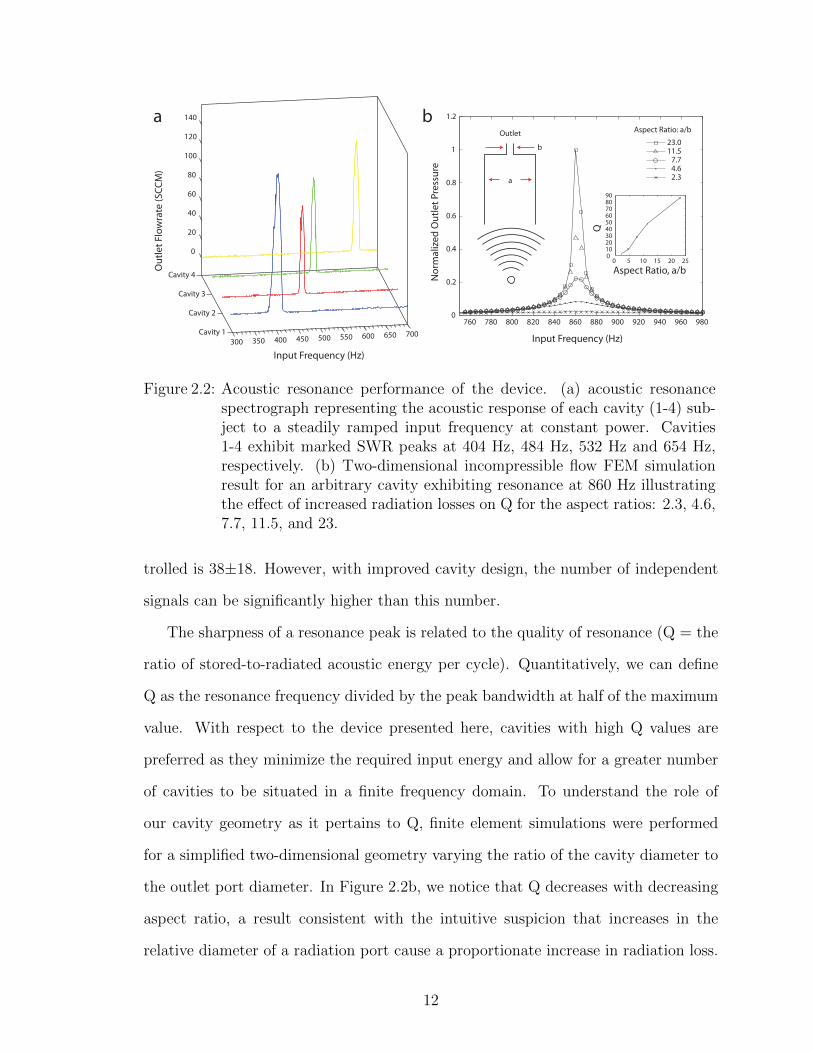
b
760 780 800 820 840 860 880 900 920 940 960 9800
0.2
0.4
0.6
0.8
1
1.2
23.011.5
7.74.62.3
Aspect Ratio: a/b
b
a
Outlet
Input Frequency (Hz)
No
rma
lize
d O
utl
et
Pre
ssu
re
Aspect Ratio, a/b
Q
0 5 10 15 20 250102030405060708090
a
Input Frequency (Hz)
Ou
tle
t F
low
rate
(S
CC
M)
300 350 400 450 500 550 600 650 700Cavity 1
Cavity 2
Cavity 3
Cavity 4
0
20
40
60
80
100
120
140
Figure 2.2: Acoustic resonance performance of the device. (a) acoustic resonancespectrograph representing the acoustic response of each cavity (1-4) sub-ject to a steadily ramped input frequency at constant power. Cavities1-4 exhibit marked SWR peaks at 404 Hz, 484 Hz, 532 Hz and 654 Hz,respectively. (b) Two-dimensional incompressible flow FEM simulationresult for an arbitrary cavity exhibiting resonance at 860 Hz illustratingthe effect of increased radiation losses on Q for the aspect ratios: 2.3, 4.6,7.7, 11.5, and 23.
trolled is 38±18. However, with improved cavity design, the number of independent
signals can be significantly higher than this number.
The sharpness of a resonance peak is related to the quality of resonance (Q = the
ratio of stored-to-radiated acoustic energy per cycle). Quantitatively, we can define
Q as the resonance frequency divided by the peak bandwidth at half of the maximum
value. With respect to the device presented here, cavities with high Q values are
preferred as they minimize the required input energy and allow for a greater number
of cavities to be situated in a finite frequency domain. To understand the role of
our cavity geometry as it pertains to Q, finite element simulations were performed
for a simplified two-dimensional geometry varying the ratio of the cavity diameter to
the outlet port diameter. In Figure 2.2b, we notice that Q decreases with decreasing
aspect ratio, a result consistent with the intuitive suspicion that increases in the
relative diameter of a radiation port cause a proportionate increase in radiation loss.
12
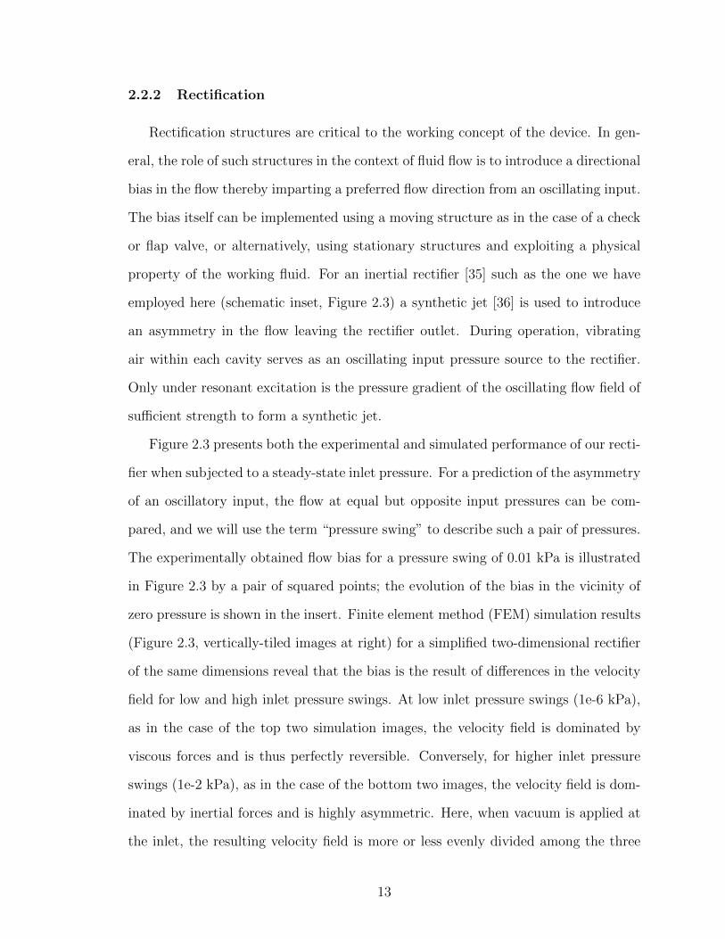
2.2.2 Rectification
Rectification structures are critical to the working concept of the device. In gen-
eral, the role of such structures in the context of fluid flow is to introduce a directional
bias in the flow thereby imparting a preferred flow direction from an oscillating input.
The bias itself can be implemented using a moving structure as in the case of a check
or flap valve, or alternatively, using stationary structures and exploiting a physical
property of the working fluid. For an inertial rectifier [35] such as the one we have
employed here (schematic inset, Figure 2.3) a synthetic jet [36] is used to introduce
an asymmetry in the flow leaving the rectifier outlet. During operation, vibrating
air within each cavity serves as an oscillating input pressure source to the rectifier.
Only under resonant excitation is the pressure gradient of the oscillating flow field of
sufficient strength to form a synthetic jet.
Figure 2.3 presents both the experimental and simulated performance of our recti-
fier when subjected to a steady-state inlet pressure. For a prediction of the asymmetry
of an oscillatory input, the flow at equal but opposite input pressures can be com-
pared, and we will use the term “pressure swing” to describe such a pair of pressures.
The experimentally obtained flow bias for a pressure swing of 0.01 kPa is illustrated
in Figure 2.3 by a pair of squared points; the evolution of the bias in the vicinity of
zero pressure is shown in the insert. Finite element method (FEM) simulation results
(Figure 2.3, vertically-tiled images at right) for a simplified two-dimensional rectifier
of the same dimensions reveal that the bias is the result of differences in the velocity
field for low and high inlet pressure swings. At low inlet pressure swings (1e-6 kPa),
as in the case of the top two simulation images, the velocity field is dominated by
viscous forces and is thus perfectly reversible. Conversely, for higher inlet pressure
swings (1e-2 kPa), as in the case of the bottom two images, the velocity field is dom-
inated by inertial forces and is highly asymmetric. Here, when vacuum is applied at
the inlet, the resulting velocity field is more or less evenly divided among the three
13

inlet outlet
vent
vent
Recti�cation Structure
500
Inlet Pressure (kPa)
Ou
tle
t F
low
Ra
te (
SC
CM
)
−0.04 −0.03 −0.02 −0.01 0 0.01 0.02 0.03 0.04
−200
−100
0
100
200
300
400
1e-6 kPa
-1e-6 kPa
1mm
-0.01 kPa
0.01 kPa
x 10−3
Inlet Pressure Swing (kPa)
Flo
w B
ias
(SC
CM
)
0 1 2 3 4 5 6 7
0
50
100
150
200
250
300
Re
cti
�e
r T
hre
sh
old
Figure 2.3: Rectifier outlet flow subject to ±0.03 kPa of inlet air pressure. (main plot)Experiment showing the resulting rectifier outlet flow rate over a rangeof inlet pressures. (inset plot) Evolution of rectifier flow bias computedas the difference in outlet flow rate at a given pressure swing. Bias at±0.02 kPa represented as a pair of squared points. (inset schematic) Two-dimensional rectifier geometry used in FEM simulations. (images at right)Velocity field snapshots from FEM two-dimensional incompressible flowsimulations. The top two images show the reversible viscous dominantflow field for extremely small inlet pressures ±1e-6 kPa. The bottomtwo images show the inertial dominant flow field at a pressure swing of±0.01 kPa. Marked differences in the velocity field emerge due to flowseparation and jetting at the rectifier inlet mouth.
14

remaining ports; however, application of a positive inlet pressure leads to the forma-
tion of a synthetic jet which extends from the mouth of the rectifier inlet toward the
outlet. Application of a sinusoidally varying inlet pressure of sufficient strength then
leads to a net unidirectional flow at the rectifier outlet. Thus the presence or absence
of resonant tones allows us to jump between inertial- and viscous-dominated regimes
thereby precisely controlling the state and level of each cavity output pressure.
2.2.3 Acoustically-Driven Liquid Motion
To illustrate the power of this concept for applications in microfluidic flow control,
the device was connected to a polydimethylsiloxane (PDMS) chip with four parallel
input channels each containing a 3 µL water droplet (Figure 2.4a). Prescribed se-
quences of resonant notes, each being responsible for the actuation of a single drop,
were then used to selectively actuate droplets. Droplet velocity in response to the
acoustic input signal is shown in Figure 2.4b. Acoustic input signals consisting of
both single notes and chords produce instantaneous and targeted droplet motion, as
shown in Figure 2.4b. To illustrate the speed at which instructions can be carried out,
the tone durations in this experiment were kept brief (≈0.2 sec) amounting to droplet
displacements on the order of 0.2-0.5 mm per pulse. However, computerized wave-
form construction allows for full customization of the tonal input. Thus, a droplet
can easily be moved over a longer distance or at a faster pace simply by adjusting the
amplitude and duration of the corresponding wave component.
Although equal tone amplitudes of the input waveform do not produce uniform
droplet velocities, the amplitude can easily be adjusted to compensate for this effect.
In Figure 2.4, for example, with the audio amplifier set to output 7.92 V for an input
wave amplitude of 1.0, the amplitudes resulting in the uniform movement of droplets
A, B, C, and D were: 0.77 (404 Hz), 0.90 (484 Hz), 1.23 (532 Hz), and 1.42 (654 Hz),
respectively. Increased voltage was necessary for higher frequency cavities because
15

0
100
200
300
400
500
600
Inp
ut
Sig
na
l (H
z)
Droplet D
Droplet C
Droplet B
Droplet A
0 1 2 3 4 5 6 7 8−0.5
0
0.5
1.0
1.5
2.0
Time (s)
Dro
ple
t V
elo
city
(m
m/s
)a
b
10
4
A
B
C
D
404 Hz
484 Hz
532 Hz
654 Hz
resonance cavity array device containing droplets
Figure 2.4: Multiplexed droplet motion. (a) Schematic representation of experimentalsetup depicting an input acoustic signal delivered to an array of resonancecavities, each of which is linked to an input on a microfluidic device (notto scale). (b) Input acoustic signal and resulting droplet velocity as afunction of time illustrating programmed actuation of specific droplets inresponse to resonant musical tones supplied to the device. Chord ampli-tudes used to produce uniform droplet velocities were: B-C (0.89, 0.85),A-D (0.76, 1.39), A-C-D (0.80, 1.18, 1.25), and A-B-C-D (0.76, 0.76, 0.90,1.25).
16
speaker diaphragm displacement, and as such, cavity output, is frequency dependent.
In addition to the normalization of single tones, amplitudes were also adjusted within
chords as early experiments exhibited a systematic enhancement of droplet velocity
that appeared to be unique to each chord most likely due to frequency specific wave
coherence. Amplitude multipliers unique to each chord were obtained, as in the case
of single droplets, by monitoring droplet motion over many chord pulses. Despite
efforts to ensure perfectly uniform droplet motion, however, variations of up to 20 %
(on average) still exist due to fabrication inhomogeneities (Figure 2.4b).
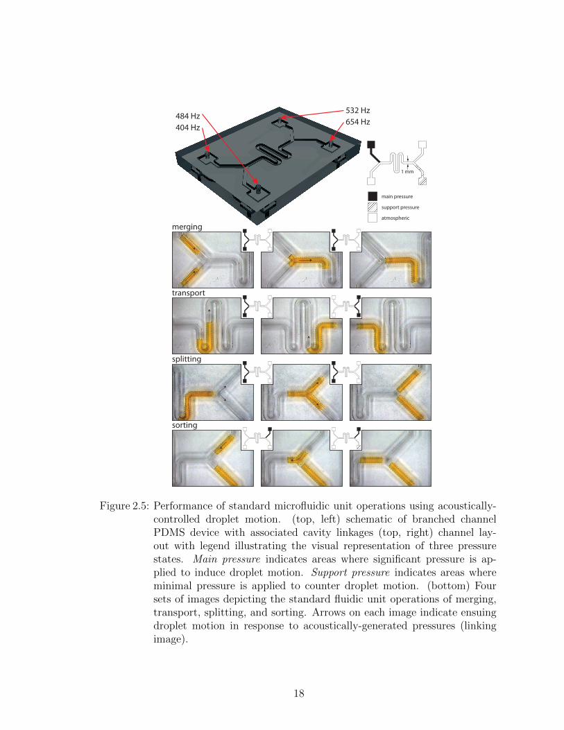
To demonstrate the use of this scheme for the operation of more complex systems,
the device was used to direct discrete drop motion within a network of pneumatically-
coupled channels. In contrast to the parallel channel network shown in Figure 2.4, a
branched network often necessitates the combination of multiple inputs to carry out
a specific fluidic operation. Figure 2.5 illustrates how the four control inputs of the
device were used to perform the standard fluidic unit operations of merging, mixing,
transport, sorting, and splitting. To ensure precise operation, droplets were actuated
in a pulsatile fashion, a strategy that is preferred when maneuvering one or more liquid
slugs near a pressure node or junction. For example, during the splitting operation
shown in Figure 2.5, the velocities of the two daughter droplets approximately double
upon splitting. Use of continuous pressure control in this case would lead to a run-
away of the resulting two slugs, a problem that is easily circumvented by shortening
the timescale of the driving pressure. Conversely, for cases in which pulsatile control
is not preferred such as for droplet transport over long distances or continuous flow
operations, the device output can be readily converted to continuous operation.
In addition to propelling individual drops, the system we describe can also be
used to pump continuous streams of fluid. Figure 2.6 illustrates how the device,
when operated in continuous output mode, can be used to generate customizable
acoustically-switchable concentration gradients. In the experiment, dynamically re-
17
654 Hz
532 Hz484 Hz
404 Hz
main pressure
support pressure
atmospheric
1 mm
merging
transport
splitting
sorting
Figure 2.5: Performance of standard microfluidic unit operations using acoustically-controlled droplet motion. (top, left) schematic of branched channelPDMS device with associated cavity linkages (top, right) channel lay-out with legend illustrating the visual representation of three pressurestates. Main pressure indicates areas where significant pressure is ap-plied to induce droplet motion. Support pressure indicates areas whereminimal pressure is applied to counter droplet motion. (bottom) Foursets of images depicting the standard fluidic unit operations of merging,transport, splitting, and sorting. Arrows on each image indicate ensuingdroplet motion in response to acoustically-generated pressures (linkingimage).
18
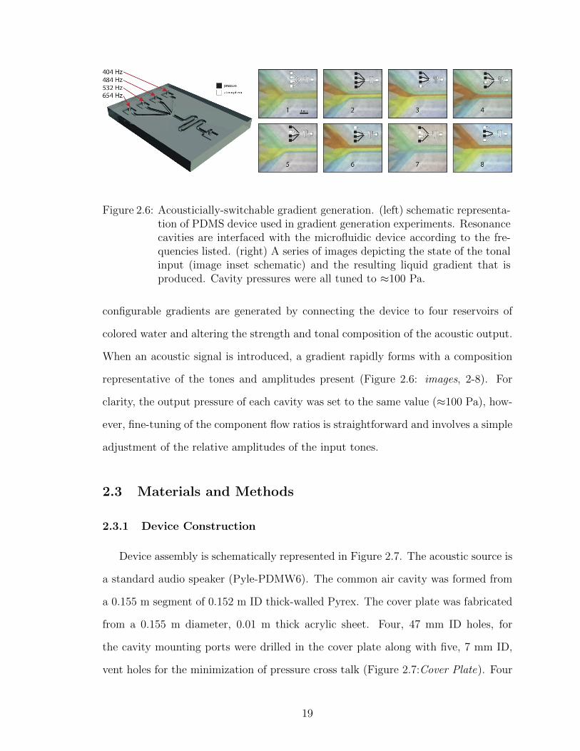
Figure 2.6: Acousticially-switchable gradient generation. (left) schematic representa-tion of PDMS device used in gradient generation experiments. Resonancecavities are interfaced with the microfluidic device according to the fre-quencies listed. (right) A series of images depicting the state of the tonalinput (image inset schematic) and the resulting liquid gradient that isproduced. Cavity pressures were all tuned to ≈100 Pa.
configurable gradients are generated by connecting the device to four reservoirs of
colored water and altering the strength and tonal composition of the acoustic output.
When an acoustic signal is introduced, a gradient rapidly forms with a composition
representative of the tones and amplitudes present (Figure 2.6: images, 2-8). For
clarity, the output pressure of each cavity was set to the same value (≈100 Pa), how-
ever, fine-tuning of the component flow ratios is straightforward and involves a simple
adjustment of the relative amplitudes of the input tones.
2.3 Materials and Methods
2.3.1 Device Construction
Device assembly is schematically represented in Figure 2.7. The acoustic source is
a standard audio speaker (Pyle-PDMW6). The common air cavity was formed from
a 0.155 m segment of 0.152 m ID thick-walled Pyrex. The cover plate was fabricated
from a 0.155 m diameter, 0.01 m thick acrylic sheet. Four, 47 mm ID holes, for
the cavity mounting ports were drilled in the cover plate along with five, 7 mm ID,
vent holes for the minimization of pressure cross talk (Figure 2.7:Cover Plate). Four
19

resonance cavities were formed from 47 mm ID, 51 mm OD, borosilicate tube stock
cut to 192 mm, 156 mm, 141 mm, and 111 mm, respectively. Cavities were sealed
at one end, save for a small 2 mm ID, 10 mm long, borosilicate rectifier inlet port.
Rectification structures consist of a 2 mm ID port which extends slightly into the
confluence of a three-way cross formed by fusing three lengths of 4mm ID, 6 mm OD
pyrex tubing (Figure 2.7: Resonance Cavity/Rectifier). All of the components in the
final assembled device were joined using an off-the-shelf RTV silicone except for the
rectification structure which was joined using a durable epoxy.
2.3.2 Measurement of Cavity Resonance
A constant voltage analog signal was generated using Labview (PCI-6031E) and
amplified using a standard audio amplifier (Audiosource, AMP-100). In a typical ex-
periment, the input waveform was steadily ramped from 300-800 Hz and the resulting
output flow rate was monitored using a custom hot-wire anemometer and bridge cir-
cuit. Flow measurements were taken by placing the anemometer just proud of the
rectifier outlet port and surrounding the assembly with a paper cylinder to minimize
disturbance from ambient air currents.
2.3.3 Rectifier Flow Bias
For positive gauge pressures, air was delivered to the rectifier inlet using a mass
flow controller (MKS, 11598B-05000SV). Application of negative gauge pressure was
performed using a two-stage vacuum regulator in conjunction with a house vacuum
source. In each case, the inlet pressure was monitored with a strain gauge (Omega,
DP-25B-S) extending from a T-junction just prior to the rectifier inlet. Outlet flow
rate was monitored using a custom hot wire anemometer and bridge circuit.
20

Resonance Cavity/Recti�er
2 mm ID
4 mm ID
40 mm
192 mm ID
156 mm ID
141 mm ID
111 mm ID
10 mm
47 mm ID
Cover Plate
7 mm ID
47 mm
0.155 m ID
Cover Plate
Common Cavity
Speaker
to Ampli�er &
Signal Source
Recti�er
Resonance Cavity
Outlet
Figure 2.7: Device construction. (top) Exploded schematic view of device. (bottom)Detail of Cover Plate and Resonance Cavity/Recitifer with dimensions
21
2.3.4 Programmed Droplet Motion
Droplet experiments shown in Figures 2.4 and 2.5 were performed by coupling
resonance cavity outlets to a nearby PDMS device using standard silicone tubing
and syringe tip connections. The PDMS devices were fabricated using standard soft
lithography protocols with 1000 µm wide by 500 µm deep channels. PDMS provides
an ideal hydrophobic substrate on which to perform these experiments, as the non-
wetting properties of the material eliminate the problems of droplet pullback and
volume loss that accompany wetting surfaces. Prior to the experiment, a 3 µL colored
water droplet was loaded into each channel using a micropipette. To induce droplet
motion, computer-generated sequences of tones and chords with various amplitudes
and durations were delivered to the device through a standard audio amplifier. The
resulting droplet motion was captured using a stationary video post integrated into
the optics of a stereomicroscope. Droplet velocities were later calculated from the
video footage using a frame analysis algorithm.
2.3.5 Gradient Generation
The PDMS chip shown in Figure 2.6 was secured to the microscope stage and
interfaced to the device using 4 mm ID silicone tubing. Gradients were generated
by setting cavity output pressures to roughly 100 Pa and varying the combination
of tones presented to the device. Reservoirs were created by filling a length of tube
leading up to the device with dyed water. Both the reservoirs and the discharge
line were fixed in level positions at the same height to eliminate hydrostatic driving
pressures. The discharge line was fitted with a 1 mm ID plastic syringe tip cut to
a shallow angle to minimize the pressure buildup associated with drop formation;
however, periodic buildup and release of pressure associated with droplet formation
at the outlet can still be seen during operation.
22

2.4 Conclusions
This work introduces a novel acoustic-based approach to distributed pressure con-
trol. In a process that can be likened to fiber optic communication, the device we have
fabricated utilizes elements of acoustic resonance, fluidic rectification, and computer
control in a simple arrangement to generate multiple, independently-addressable out-
put pressures in the range of 0-200 Pa (control resolution of ≈10 Pa) that can be
operated via a single control line. The device was interfaced to both droplet-based
and continuous flow microfluidic systems and used to carry out various operations
such as merging, transport, splitting, sorting, and on-demand gradient generation.
Future devices may be scaled down and employ alternative methods of signal genera-
tion such as the direct displacement of a sealed cavity using piezoelectric transducers,
or non-contact vibration of a flexible membrane using a remote acoustic source. De-
velopment of an on-chip equivalent to the device presented here could greatly simplify
operation of complex lab-on-a-chip devices potentially extending the application base
of such tools to non-scientists.
23

CHAPTER III
VARIED EFFECTS OF PHONONIC CRYSTAL
LATTICE GEOMETRY ON THE EMERGENCE
AND EVOLUTION OF TRANSMISSION BAND
GAPS
3.1 Introduction
Phononic crystals represent an intriguing subclass of metamaterials whose physical
structures have the capacity to shape acoustic transmission. Long known to exhibit
band gap effects under certain circumstances, phononic crystal materials have gar-
nered a good deal of attention recently because of their looming potential in the
areas of vibration and noise-control [37–39], imaging [40, 41], RF communications
[42], waveguides [43–45], and filters [46, 47]. Much of this recent popularity is also
attributable to advances in microfabrication techniques, prior to which, the physical
realization of phononic crystals was largely limited to macroscopic structures consist-
ing of hand-assembled balls and rods [48–50]. The area of microfabricated phononic
systems and devices is particularly interesting now, as researchers are developing
methods to couple various device components (e.g., CMOS circuitry, photonic crys-
tals, and piezoelectrics) alongside phononic materials, creating an unprecedented level
24

of integration [51–53].
Traditionally, phononic crystals are binary composites possessing a periodic dis-
tribution of scattering centers; though some researchers have examined the potential
utility of more complex hybrids [54]. Such composites can be solid/solid, fluid/fluid,
or fluid/solid and typically consist of isolated scattering elements, or inclusions, em-
bedded in a continuum host matrix [55]. Transmission gaps can be opened in these
structures when the reflections sourced from a collection of individual scattering cen-
ters are in-phase — for plane wave propagation this is the Bragg or half wavelength
resonance condition related to the spatial distribution of the inclusions along the po-
larization direction — thus forming a standing wave throughout the lattice which
serves to reflect incident acoustic energy. In addition to the spatial periodicity of the
crystal, inclusion shape has also been reported to influence gap formation [56]. The
influence of inclusion shape is particularly significant at higher frequencies (acoustic
wavelength comparable to inclusions dimensions) where multiple scattering effects
become dominate. Surprisingly, while the vast majority of the literature is devoted
to studying various criteria related to band gap formation, for these and other lattice
properties, the exploration of the band gap effects related to the varied effects of
lattice geometry has remained cursory.
In this work, we report on the influence of various geometric parameters as they
pertain to the band gap properties of finite, two-dimensional phononic crystals. We
discuss the utility of simplified analytical approximations as well as the analysis of
phononic crystals in their infinite limit as tools for the modeling and interpretation
of crystal transmission. The work is organized as follows: We first discuss the use
of the finite element method (FEM) to simulate the transmission profiles of duct-
confined two-dimensional (2D) phononic crystals subject to a variety of geometric
perturbations of the crystal lattice. We then utilize a one-dimensional (1D) transfer
matrix method approximation to model the location and contour of band gaps —
25

taking the view that the spatial periodicity of the 2D crystal, subject to plane wave
excitation, is functionally equivalent to a 1D duct consisting of a series of rectangular
constriction and expansion segments. Lastly, for comparison with the simulated 2D
FEM transmission profiles, we compute band structures for the corresponding infinite
phononic crystals and discuss their utility as tools for analyzing finite systems.
3.2 Theory
The base FEM simulation geometry examined in this work consisted of a 2D
phononic crystal array confined within a semi-infinite duct in the x-y plane (Figure
3.1a). In each case, the y-dimension of the array, nyay, was scaled as to completely
span the transverse dimension of the duct (nyay ≥ Sduct), which was fixed at 1.0
cm. The longitudinal array width (nxax), unless otherwise specified, was fixed at five
columns of incusions (nx = 5). The array itself was composed of cylindrical inclusions
with semi-axis radii, rx and ry, and spacing described by the pair of primitive lattice
constants ax and ay, as illustrated in Figure 3.1b. As a central point of discussion,
we define as our base case geometry, the simple cubic arrangement shown in Figure
3.1b in which the lattice constants ax and ay are equal to 1000 µm or abase, and
the inclusion radii, rx and ry, are equal to 250 µm or rbase. In the FEM model, we
utilize the Helmholtz formulation of the elastic wave equation [57] and impose the rigid
boundary condition for both the duct and inclusion walls. For the inlet and outlet duct
boundaries, we imposed the radiation condition to ensure the absence of unwanted
reflections. Additionally, at the inlet boundary we introduce a rightward traveling
plane wave with pure x-polarization and unit amplitude. The elastic medium under
consideration is air. Transmission profiles were generated by conducting a parametric
sweep of the frequency domain (1kHz-1MHz) while simultaneously monitoring sound
pressure levels at the inlet and outlet duct boundaries. The confining duct area being
constant, intensity transmission coefficients were computed as the magnitude squared
26
(a)
(c) (d)
(b)
ax
rx
ry
ay
. . .
. . .
. . .
. . .. . .
. . .
. . .
. . .
x
yn y
a y
nxax
Sduct
. . .
L2
S2S1Pin
Uin
Pout
Uout
L1NΛ
Λ
Si
xleft xright
Li
Pleft
Uleft
Pright
Uright
Figure 3.1: Simulation and model geometries: (a) FEM model system geometry con-sisting of a finite phononic crystal lattice composed of rigid cylindrical orelliptical inclusions confined to a semi-infinite rigid walled duct in the x-yplane. (b) Detail of phononic crystal lattice comprising rigid cylindricalinclusions with semi-axis radii rx and ry (for base case, rx = ry = 250µm) and spacing defined by the lattice constants ax and ay (for base case,ax = ay = 1000 µm). (c) Generic duct segment used in the formulationof the TMM model (d) Schematic illustration of the 1D TMM approxi-mation applied to an N periodic lattice of period length Λ.
of the ratio of transmitted to incident amplitudes.
The transfer matrix method (TMM) — which relates the total pressure and vol-
ume velocity between two points in an elastic medium via a transfer matrix — is
particularly useful for modeling the acoustic response of 1D periodic structures such
as waveguides. Our utilization of the TMM is based on the assumption that, for plane
wave propagation and ax polarization, the 2D array of inclusions shown in Figures
3.1a and 3.1b can be represented by a 1D duct consisting of rectangular constriction
and expansion segments linked in series. Formulation of the TMM begins by solving
27

for the transfer matrix of a generic duct segment assumed to exist on the interval
(xleft , xright) as shown in Figure 3.1c. The total pressure at the left and right of this
segment (neglecting viscous losses) can be described by the wave function
p(x, t) = P (x, t)ejωt (3.1)
where the spatial component of the total pressure at the duct extremities is an
assumed superposition of rightward and leftward traveling waves
P (x, t) =
Aejkx + Be−jkx (x < xleft)
Cejkx + De−jkx (x > xright)
=
Pleft
Pright
(3.2)
with complex amplitude coefficients A, B, C, and D, and k = ω/c is the wave
number (where ω is the angular frequency and c is the characteristic speed of sound
in air). Application of the Euler relation to Eqn.3.2 and multiplying by the duct area,
S(x), the corresponding spatial component of the volume velocity is found to be
U(x, t) =
S(x)ρoc
(Aejkx − Be−jkx
)(x < xleft)
S(x)ρoc
(Cejkx − De−jkx
)(x > xright)
=
Uleft
Uright
(3.3)
where ρo is the ambient density of air. The total pressure and volume velocity at
the duct boundaries can thus be represented by the matrix expression
(Pleft
Uleft
)= T
(Pright
Uright
)(3.4)
where T is the transfer matrix whose components are related to the amplitude
coefficients A, B, C, and D. Solving for the complex amplitude coefficients then gives
the transfer matrix for a generic waveguide segment of length Li = xright − xleft , and
28
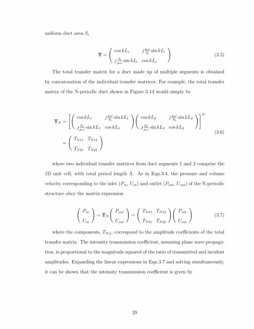
uniform duct area Si
T =
(cos kLi j ρoc
Sisin kLi
j Si
ρocsin kLi cos kLi
)(3.5)
The total transfer matrix for a duct made up of multiple segments is obtained
by concatenation of the individual transfer matrices. For example, the total transfer
matrix of the N-periodic duct shown in Figure 3.1d would simply be
TN =
[(cos kL1 j ρoc
S1sin kL1
j S1
ρocsin kL1 cos kL1
)(cos kL2 j ρoc
S2sin kL2
j S2
ρocsin kL2 cos kL2
)]N ‘
=
(TN11 TN12
TN21 TN22
) (3.6)
where two individual transfer matrices from duct segments 1 and 2 comprise the
1D unit cell, with total period length Λ. As in Eqn.3.4, the pressure and volume
velocity corresponding to the inlet (Pin , Uin) and outlet (Pout , Uout) of the N-periodic
structure obey the matrix expression
(Pin
Uin
)= TN
(Pout
Uout
)=
(TN11 TN12
TN21 TN22
)(Pout
Uout
)(3.7)
where the components, TNij, correspond to the amplitude coefficients of the total
transfer matrix. The intensity transmission coefficient, assuming plane wave propaga-
tion, is proportional to the magnitude squared of the ratio of transmitted and incident
amplitudes. Expanding the linear expressions in Eqn.3.7 and solving simultaneously,
it can be shown that the intensity transmission coefficient is given by
29

αt =
∣∣∣∣∣Pout
Pin
∣∣∣∣∣2
=
∣∣∣∣∣ 1
12
(TN11 + Sout
ρocTN12 + ρoc
SinTN21 + Sout
SinTN22
)∣∣∣∣∣2
(3.8)
For comparison with the FEM transmission profiles of the 2D crystals, band struc-
ture calculations of the corresponding infinite phononic crystals were performed using
the approach presented by Kuo et al [53]. In this method, unit cells of the crystal
lattice are rendered and then tiled to infinity by application of periodic boundary
conditions. Eigen frequencies contours of the first twenty propagating modes were
then computed by sweeping the Bloch wave vector in reciprocal space along the high
symmetry directions of the first irreducible Brillouin zone using a Matlab scripting
routing interfaced with COMSOL Multiphysics.
3.3 Results and Discussion
3.3.1 Effects of Lattice Geometry
Altering the geometry of a phononic crystal can have dramatic and occasionally
counterintuitive consequences on the locations and contours of transmission band
gaps. Taking as a point of departure, the base case crystal lattice in Figure 3.1b,
perhaps the most straightforward geometric alteration one can make is to vary the
nearest neighbor spacing of the inclusions. Such a change amounts to parameteri-
zation of the two principal lattice constants, ax and ay, which ultimately define the
spatial periodicity of the system. Scaling of the unit cell in these principal directions
augments the interference of incident waves and thus the location and contour of any
transmission band gaps that may exist. Other changes to crystal geometry such as
the scaling/reshaping of the inclusions or use of alternate lattice constructions are
also possible and can figure heavily into shaping band gap properties. Longitudinal
(ax) contraction or expansion of a crystal unit cell, for example, primarily results in a
marked shift in band center. The shift is most pronounced for, what will henceforth
30

be referred to as, the principal band gap, i.e., the transmission band gap associated
with the main period length of the crystal. The location of the principle gap —
assuming sonification of the lattice with ax polarized plane waves as in Figure 3.1a
— is described by the half-wavelength (λ/2 = ax) condition, or Bragg length, as
it is known in optics. FEM-simulated intensity transmission coefficients shown in
Figure 3.2a show this migration of the principal band gap for several ax spacings
relative to abase. The gap center frequencies for ax/abase equal to 0.6, 0.8, 1.0, 1.2,
and 1.4, as predicted by FEM are, respectively, 259 kHz, 201 kHz, 165 kHz, 139
kHz, and 119 kHz. Interestingly, these predictions correspond to theoretical Bragg
lengths (λ/2 = c/2f) that are slightly longer than the simulated dimensions (0.66,
0.85, 1.04, 1.23, and 1.44). This effective lengthening of the unit cell dimension ax
arises due to the radiation impedance (mass-loading) that occurs at each change in
area of the crystal. Such an impedance change gives rise to reflections which have a
periodicity that is half that of the unit cell. Consequently, small band gaps open up
at roughly twice the principal gap frequency. These gaps are fully resolvable only for
relative spacings greater than unity as those below unity get lumped in with higher
frequency multiple scattering effects, which begin at roughly 343 kHz (i.e., where the
wavelength is comparable to the inclusion diameter).
Transverse (ay) contraction or expansion of the unit cell, by contrast, has a dra-
matic effect on the bandwidth and peak loss (minimum value of the intensity trans-
mission coefficient at the gap center) of the principal band gap. Intensity transmission
coefficients obtained for several transverse spacings, again relative to the base case
(ay/abase), are shown in Figure 3.2b. We note that unlike altering the longitudinal
dimension of the crystal unit cell, a change to the transverse spacing between inclu-
sions has negligible effect on the frequency of the principal band center. This result
is more or less expected, in view of the planar x-polarization of the incident phonons.
Before looking at the effect of bandwidth in Figure 3.2b, it is helpful to consider
31

0.5
1
1.5
2
2.5
3
3.5
4
Inpu
t Fre
quen
cy (x
100
kHz)
0.5
1
1.5
2
2.5
3
3.5
4
Inpu
t Fre
quen
cy (x
100
kHz)
Intensity Transmission Coe!cient / αt
0 0.5 1
0.6
0.8
1.0
(a)
(b)
1.21.4
ax /abase
0.6 0.8 1.0 1.2 1.4ay /abase
Figure 3.2: FEM transmission profiles highlighting the location and contour of theprincipal band gap (shaded regions) subject to (a) longitudinal and (b)transverse modifications to the crystal unit cell. Spacing reported relativeto base lattice dimensions (outlined in bold).
32
the limiting cases. Extremely large vertical spacing (ay/abase � 1), for example,
represents the limit of perfect transmission; that is, the magnitude of the interference
provided by the inclusions, when spaced very far apart, goes to zero and incident
phonons at all frequencies are transmitted without attenuation. Extremely small
vertical spacing (limit as ay/abase → 0), on the other hand, represents the limit of
zero transmission. In this case, the rigid inclusions form a continuum, akin to a solid
wall, which rejects all incident acoustic energy. The profiles in Figure 3.2b illustrate
the intermediate region between these two limiting cases within which the incident
phonons are transmitted with some degree of attenuation and the bandwidth of the
principle gap scales inversely with the transverse spacing of the inclusions. At a
relative vertical spacing of 1.4, the principal gap, though prominent, is narrow in
bandwidth (76 kHz) and incomplete with a peak loss of 5e-2. At the lower end, for
a relative vertical spacing of 0.6, the principal gap bandwidth is significantly larger
(154 kHz) and the gap is essentially complete, with a peak loss of approximately 5e-5
— a three orders of magnitude reduction in intensity for roughly a 2x change to the
transverse spacing.
Apart from a scaling of the unit cell, inclusion size and shape can also heavily in-
fluence the gap properties of phononic crystals. Recent work exploring the transmis-
sion effects of substituting different inclusion shape classes such as triangles, squares,
hexagons, etc., have been reported [56]. It is found that the broadest and deepest
band gaps occurred when inclusion geometry most closely mimicked the parent lattice
structure. We chose to explore inclusion anisotropy effects by altering the longitudinal
eccentricity of the cylindrical inclusions, i.e, varying the aspect ratio of the semi-axis
radius rx, while holding ry and the base case unit cell dimensions fixed. Figure 3.3
shows the resulting FEM transmission profiles for normalized inclusion aspects ratios
(2rx/abase) from 0.1 to 0.9, where an aspect ratio of 0.5 corresponds to the neutral or
base case. We find that the principle gap center, peak loss, and bandwidth are sym-
33
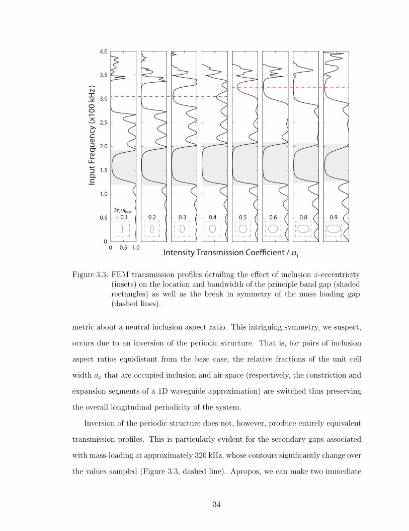
0 0.5 1.00
0.5
1.0
1.5
2.0
2.5
3.0
3.5
4.0
Inpu
t Fre
quen
cy (x
100
kHz )
Intensity Transmission Coe!cient / αt
= 0.1 0.2 0.3 0.4 0.5 0.6 0.8 0.92rx/abase
Figure 3.3: FEM transmission profiles detailing the effect of inclusion x-eccentricity(insets) on the location and bandwidth of the principle band gap (shadedrectangles) as well as the break in symmetry of the mass loading gap(dashed lines).
metric about a neutral inclusion aspect ratio. This intriguing symmetry, we suspect,
occurs due to an inversion of the periodic structure. That is, for pairs of inclusion
aspect ratios equidistant from the base case, the relative fractions of the unit cell
width ax that are occupied inclusion and air-space (respectively, the constriction and
expansion segments of a 1D waveguide approximation) are switched thus preserving
the overall longitudinal periodicity of the system.
Inversion of the periodic structure does not, however, produce entirely equivalent
transmission profiles. This is particularly evident for the secondary gaps associated
with mass-loading at approximately 320 kHz, whose contours significantly change over
the values sampled (Figure 3.3, dashed line). Apropos, we can make two immediate
34

observations with regard to the mass-loading gaps. First, the magnitude of the mass-
loading dip increases away from an inclusion aspect ratio of 0.4. Second, there is an
apparent shift in the location of the gap center frequency between the inclusion aspect
ratios 0.4 and 0.5. Qualitatively, we can understand the second observation by looking
at the length scales over which the radiation impedance occurs. For inclusions that
are highly compressed in their x-aspect (2rx/abase = 0.1), for example, the change in
area is very abrupt — occurring over just 10% of the total unit cell width (abase) —
corresponding to radiation impedance with a spacing that is 90% of the total unit cell
width. Oppositely, for elongated inclusions the impedance occurs over 90% of the unit
cell width with a spacing of the impedance of 10%. The difference in the periodicity
of the impedance, we suspect, accounts for the frequency shift observed though the
authors are perplexed as to why shift is stepwise instead of gradual. Regarding to the
first observation, the apparent minimum in the magnitude of the radiation impedance
at 0.4 rather than 0.5 is a consequence of the effective length corrections discussed
above. Specifically, the true minimum occurs where the periodicities of the waveguide
and the impedance match (theoretically 0.5); but the effect of mass-loading forces this
condition slightly down in frequency.
With regard to unit cell filling fraction (FF), the observed effect on the principal
band gap depends on the manner in which it is changed. Commonly, FF is aug-
mented via uniform scaling of the inclusions and/or unit cell. To probe for geometric
path-dependent effects, we modify FF in four distinct ways (Figure 3.4a). In Figure
3.4b and 3.4c, we show the change in both bandwidth and peak loss of the principal
gap for FFs obtained by: (1) isotropic scaling of the inclusion radii, (2) alteration of
the x-eccentricity of the inclusions, and (3-4) stretching the unit cell dimensions in
both the longitudinal and transverse directions. The data reflecting the change to
the bandwidth (Figure 3.4b) exhibits trajectories of two distinct magnitudes. The
shallower of the two trajectories relates to geometric modification of the inclusions,
35

(b)(a) (c)
0 0.1 0.2 0.3 0.410−2
10−1
100
101
102
Filling Fraction
Peak
Los
s (re
lativ
e to
bas
e ca
se)
inclusion scaling unit cell - longitudinal
unit cell - transverseinclusion x-eccentricity
Band
wid
th (r
elat
ive
to b
ase
case
)
0 0.2 0.4 0.6 0.80.5
1.0
1.5
2.0
Filling Fraction
inclusionscalinginclusionx-eccentricityunit cell-longitudinalunit cell-transverse
Figure 3.4: Influence of filling fraction ratio (FF). (a) Schematics detailing the fourgeometric paths taken in the modification of the FF. (b) Bandwidth (nor-malized to base case) of the principal band gap as a function of FF. (c)Peak loss of the intensity transmission coefficient (normalized to basecase) of the principal band gap as a function of FF.
and the steeper of the two, to changes in the unit cell dimensions. Not surprisingly,
in the vicinity of the principal gap, changes in the unit cell dimensions (ax and ay)
exhibit the stronger dependence — a result of the changing Bragg length mentioned
above. Only at higher frequencies (wavelengths comparable to the inclusion dimen-
sions, λ/2 ≤ 2r), where multiple scattering effects become dominant, would changes
to inclusion geometry begin to compete with unit cell effects. Approximately linear
trajectories are observed in each case, save the parabolic trajectory associated with
inclusion eccentricity. This parabolic contour is tied to the inversion of the periodic
structure mentioned above.
For peak loss, the division of trajectories occurs instead between longitudinal and
transverse modifications to the crystal geometry — though arguably the scaling of
inclusion radius in this case qualifies as both. Peak loss (Figure 3.4c) values obtained
for isotropic scaling of the inclusion radius and transverse lattice spacing decreases
exponentially for successively larger FF. Qualitatively, this observation can be under-
stood by considering that an increase in FF via these parameters yields geometries
that increasingly resemble a solid wall. More interesting though, are the parabolic
36

contours associated inclusion eccentricity and longitudinal spacing. Qualitatively, the
best peak loss is achieved when the amplitude of the standing wave in the gap region
is strongest. Physically, this situation occurs near the base case (FF=0.2), where re-
flections from all perturbations in the waveguide are in phase, i.e. when the inclusion
width is exactly one half of the total period length.
Interestingly, use of alternate lattice constructions does not guarantee unique
band gap properties. For example, the principal gap profiles obtained for the square
to rhombic lattice transformation are essentially insensitive to the geometric recon-
struction. Figure 3.5a shows the transmission profiles of the base case to rhombic
transformation, which is accomplished by introducing a vertical shift (yshift) between
consecutive columns of inclusions, as illustrated in Figure 3.5b. That this oblique
character does little in the way of effecting the location and contour of the principal
band gap is somewhat counterintuitive, as one might expect the staggered arrange-
ment of inclusions to reject a greater fraction of incident acoustic energy relative to
the base case. However, in the vicinity of the principal gap—where only plane waves
propagate and the acoustic wavelength is long compared to the array spacing— the
impedance characteristics of a single air aperture will behave identically to that of
two smaller apertures of the same length and equivalent total area operating in par-
allel (Figure 3.5c). Thus, the transmission profiles measured on the other side of the
crystal slab are blind to the geometric transformation of the lattice. This reasoning
of course does not apply at high frequencies or in cases where damping is especially
prevalent. Another interesting facet of this transformation is the extinction of the
mass-loading gap. As mentioned above, this peak forms as a result of the mass-loading
at each change in area of the modulated structure, effectively introducing an addi-
tional periodicity into the system and thus an additional excitable resonance. Decay
of this peak as well as the increase in noise likely occurs because the vertical shifting
of the crystal into non-symmetric arrangements introduces destructive interference
37

Figure 3.5: FEM transmission profiles highlighting the rhombic transformation of thebase case lattice. (a) Simulated profiles reflecting a steady rhombic trans-formation of the base case lattice. (b) Schematic illustration of the trans-formation, performed by introduction of vertical shift (yshift = Φabase)between consecutive inclusion columns. (c) Pressure field images fromFEM for Φ = 0 and Φ = 0.5.
thus eliminating the resonance associated with the radiation impedance.
3.3.2 Analytical Modeling
Full-fledged phononic crystal simulations are computationally intensive and chal-
lenging to implement. We employ a 1D TMM model for predicting phononic crystal
transmission, a computationally leaner alternative which, despite its simplicity, capa-
bly reproduces the 2D FEM principal gap profiles for all of the geometric parameters
sampled here. To serve as a base for comparison, we initially seed our TMM model
with the FEM-simulated dimensions corresponding to the base case lattice. The re-
sulting 1D unit cell, shown in Figure 3.6a, is constructed from two duct segments: (1)
a constriction segment of length, L1, and width, S1, which corresponds to the aper-
ture between vertically neighboring inclusions and (2) an abrupt expansion segment
38
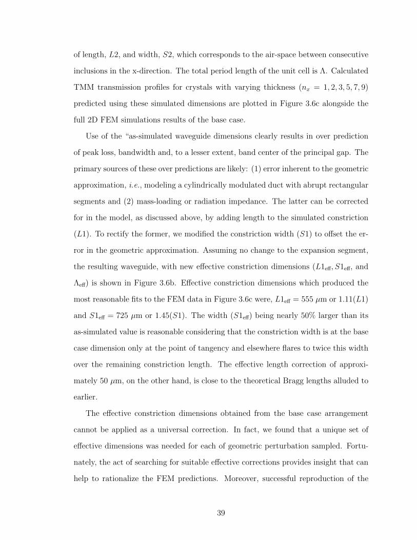
of length, L2, and width, S2, which corresponds to the air-space between consecutive
inclusions in the x-direction. The total period length of the unit cell is Λ. Calculated
TMM transmission profiles for crystals with varying thickness (nx = 1, 2, 3, 5, 7, 9)
predicted using these simulated dimensions are plotted in Figure 3.6c alongside the
full 2D FEM simulations results of the base case.
Use of the “as-simulated waveguide dimensions clearly results in over prediction
of peak loss, bandwidth and, to a lesser extent, band center of the principal gap. The
primary sources of these over predictions are likely: (1) error inherent to the geometric
approximation, i.e., modeling a cylindrically modulated duct with abrupt rectangular
segments and (2) mass-loading or radiation impedance. The latter can be corrected
for in the model, as discussed above, by adding length to the simulated constriction
(L1). To rectify the former, we modified the constriction width (S1) to offset the er-
ror in the geometric approximation. Assuming no change to the expansion segment,
the resulting waveguide, with new effective constriction dimensions (L1eff, S1eff, and
Λeff) is shown in Figure 3.6b. Effective constriction dimensions which produced the
most reasonable fits to the FEM data in Figure 3.6c were, L1eff = 555 µm or 1.11(L1)
and S1eff = 725 µm or 1.45(S1). The width (S1eff) being nearly 50% larger than its
as-simulated value is reasonable considering that the constriction width is at the base
case dimension only at the point of tangency and elsewhere flares to twice this width
over the remaining constriction length. The effective length correction of approxi-
mately 50 µm, on the other hand, is close to the theoretical Bragg lengths alluded to
earlier.
The effective constriction dimensions obtained from the base case arrangement
cannot be applied as a universal correction. In fact, we found that a unique set of
effective dimensions was needed for each of geometric perturbation sampled. Fortu-
nately, the act of searching for suitable effective corrections provides insight that can
help to rationalize the FEM predictions. Moreover, successful reproduction of the
39

0 0.5 1
0.5
0
1
1.5
2
2.5
3
3.5
Inpu
t Fre
quen
cy (
Hz
x105 )
Intensity Transmission Coe!cient / αt
FEMSimulatedE"ective
L1
S1 S2
L2
Λ
Simulated Dimensions
L1e"
S1e" S2
L2
Λe"
E"ective Dimensions
(a)
(b)
(c)
Figure 3.6: Transfer matrix (TMM) model results for crystals of varying thickness.(a-b) Schematic of simulated and effective 1D waveguide dimensions usedin TMM model. (c) Transmission profiles for duct-confined phononiccrystals of varying thickness (left to right, nx = 1, 2, 3, 5, 7, 9) as predictedby FEM (solid black curves). TMM model results based on simulated(dashed blue curves) waveguide dimensions (L1, S1, L2, S2) and effective(dashed red curves) waveguide dimensions (L1eff, S1eff, L2, S2).
40

0.5 1 1.5 21
1.1
1.2
1.3
1.4
1.5
1.6
Longitudinal Spacing
E!ec
tive
Cons
tric
tion
Dim
ensio
ns (r
elat
ive
to “a
s sim
ulat
ed” v
alue
s)
0.5 1 1.5
1
1.5
2
2.5
3
3.5
Transverse Spacing
0 0.5 1 1.5 20.8
1
1.2
1.4
1.6
Inclusion X−Eccentricity
0 0.5 1 1.5 20. 5
1
1.5
2
2.5
Inclusion Radius
(a) (b)
(c) (d)
L1e! /L1
(ax /abase) (ay /abase)
(rx /rbase) (r /rbase)
S1e! /S1
Figure 3.7: Effective constriction dimensions relative to as simulated values. (a) lon-gitudinal spacing relative to abase, (b) transverse spacing relative to abase,(c) inclusion x-eccentricity relative to rbase (d) inclusion radius relative torbase.
FEM profiles indicates that we may analyze the transmission properties of complex
2D crystals within the framework of simple 1D waveguides, which are intuitively more
tractable. The effective constriction parameters for each of the geometric alterations
of the lattice discussed so far are shown in Figure 3.7.
The required effective corrections corresponding to longitudinal contraction of ex-
pansion of the unit cell are shown in Figure 3.7a. Relative longitudinal spacings
— achieved by varying the L2 dimension of the 1D unit cell — less than unity
(ax < abase), the normalized effective constriction dimensions, expressed as the ratio
41

of the effective to simulated dimension (L1eff/L1 and S1eff/S1), approach the limit
corresponding to no correction or unity on the ordinate axis (Figure 3.7a). The decline
in the required correction for tighter longitudinal spacing reflects the disappearance
of expansion segment L2, or more simply, the waveguide increasingly resembles an
unperturbed 1D duct. For spacing greater than unity, the effective constriction di-
mensions, as one might expect given that the aspect ration of the constriction is non-
changing, become insensitive to changes in longitudinal spacing, leveling off near the
effective dimensions obtained for the base case (L1eff/L1 ≈ 1.1, and S1eff/S1 ≈ 1.45).
Unlike the longitudinal case, changing the transverse spacing (S1) represents an
actual modification to the aspect ratio of the constriction. The effective constriction
dimensions obtained for transverse spacing are plotted in Figure 3.7b. We see that
for large transverse spacing (ay > abase), the width correction (S1eff/S1) approaches
unity, whereas, for small spacing (ay < abase) it grows to nearly three times the base
case constriction dimensions. Interestingly, the absolute difference in the effective
and theoretical constriction widths is approximately constant at 214 ± 13 µm. This
difference, remaining essentially constant, is reasonable given that the cylindrical
profile of the inclusions — that intuitively should dictate the width correction — is
not changing here. Moreover, this fixed correction accounts for the observed trend in
the normalized effective width ratio, which grows rapidly for small transverse spacing
and approaches unity for arbitrarily wide constrictions. The effective constriction
length follows a trajectory that is nearly identical to the longitudinal case. This is
unexpected as effective length corrections for macroscopic flaring horns are typically
proportional to duct width.
The results for inclusion x-eccentricity are slightly more complicated (Figure 3.7c).
The effective constriction width correction, for example, is parabolic with the maxi-
mum correction occurring near the base case (rx/rbase = 1). We speculate that this
is the result of the inclusions being more geometrically accurate to their rectangu-
42

lar approximations at the extremes. In the lower limit (rx/rbase < 1), for example,
inclusions are highly compressed in their x-aspect and, as such, accurately resemble
an abrupt rectangular constriction with near vertical walls. Likewise, in the oppos-
ing limit where the inclusions are elongated in their x-aspect, the periphery of the
inclusion reasonably follows that of a long constriction. The intermediate aspects,
however, are not as close in their impression of the rectangular waveguide segments
and thus require greater width corrections. It is helpful to separately analyze the
effective length corrections in two parts. Below the base case (rx/rbase ≤ 1), the ab-
solute length correction required remains constant at 48 ± 3 µm. This is in keeping
with the relative constancy of the gap center frequency shown in Figure 3. How-
ever, when normalized to the base case, the increasing rx dimension of the inclusions
produces a rapid decline of L1eff/L1 toward unity, i.e., the condition reflecting no cor-
rection. For values above the base case (namely, rx/rbase = 1.20, 1.60, and1.80), we
find the required length corrections to be 35 µm, 16 µm, and (-23 µm), respectively.
The fact that the correction appears to become negative is perhaps reasonable if we
consider: (1) the geometric resemblance mentioned earlier for highly elongated inclu-
sions should decrease the required correction, and (2) elongated flaring horns, such
as those found in wind instruments, have been shown to exhibit negative effective
length corrections.
Scaling of the inclusion radius represents the situation in which both constriction
length and width vary simultaneously and opposite to one another (Figure 3.7d).
That is, for large radii the constriction is long and narrow whereas for small radii the
constriction is short and wide. It is important to note that with fixed base case lattice
spacing, adjustment of the inclusion radius is constrained to a dimensionless inclusion
radius (r/rbase) equal to a value of two. At this limit, the inclusion diameter is equal
to the unit cell width and the rigid inclusions form a continuum akin to a solid wall.
Near this limit, the width correction increases rapidly — analogous to the narrowing
43

of the transverse spacing in Figure 3.7b. By contrast, the length correction decreases
in the neighborhood of two eventually dropping below one, indicating a negative
length correction. This result is consistent with the negative correction observed for
the highly elongated inclusions in Figure 3.7c. An inclusion radius of zero, on the
other hand, corresponds to the physical limit in which the inclusion vanishes and the
waveguide becomes an unperturbed channel with width S2. From Figure 3.7d, we
observe that both the effective length and width corrections approach unity in the
limit where the inclusion radius vanishes. This represents the unperturbed channel
case in which S1eff approaches S2 and L1 approaches zero.
3.3.3 Band Structure Calculations
Study of phononic crystal gap formation in the infinite limit can provide signifi-
cant insight — particularly at higher frequencies where plane wave methods are no
longer valid — into the analysis of finite systems. Take, for instance, the base case
FEM transmission profiles for crystals of varying thickness (nx = 3, 5, and 9) shown
in Figure 3.8 (right panel) and the corresponding Γ − X band structure Figure 3.8
(left panel). The simulated profiles exhibit five distinct gap regions, beginning with
the principal gap at 165 kHz, where acoustic transmission is severely attenuated.
Remarkably, these gap regions correspond, at least in the case of the principal and
mass-loading gaps (labeled 1 and 2), to regions in the band structure where no prop-
agating modes are predicted to exist. Furthermore, the predicted gap locations and
gap widths appear to converge for crystals with as few as nine periodic repeats. Such
agreement bolsters the notion that band structure calculations can be used in the
analysis of finite systems
Interestingly, the higher frequency band gaps (labeled 3, 4, and 5) are not pre-
dicted in the band structure due to the presence of extraneous modes (Figure 3.8,
dashed curves) that traverse the anticipated gap regions. These modes form as a result
44
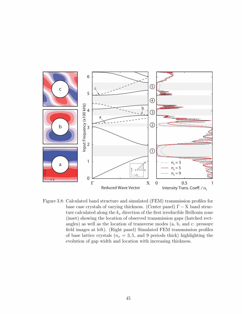
Intensity Trans. Coe!. / αtReduced Wave Vector
Γ Χ
b
0
1
2
3
4
5
6
Inpu
t Fre
quen
cy (x
100
kHz)
0 0.5 1
nx = 5nx = 9
nx = 3
Χ
Μ
Γ
a
c
1
2
3
4
5
kx
ky
x
y
c
b
a
Figure 3.8: Calculated band structure and simulated (FEM) transmission profiles forbase case crystals of varying thickness. (Center panel) Γ−X band struc-ture calculated along the kx direction of the first irreducible Brillouin zone(inset) showing the location of observed transmission gaps (hatched rect-angles) as well as the location of transverse modes (a, b, and c: pressurefield images at left). (Right panel) Simulated FEM transmission profilesof base lattice crystals (nx = 3, 5, and 9 periods thick) highlighting theevolution of gap width and location with increasing thickness.
45

of degenerate Eigen solutions (multiple geometric orientations at a single frequency
that satisfy the wave equation) which, due to their transverse character, are not (or
are only weakly) excited by the longitudinally-polarized incident waves. Transmission
profiles obtained from FEM are thus “deaf” to these modes, leading to the observa-
tion of gaps 3, 4, and 5. For visual inspection, pressure fields for these transverse
degenerates are plotted in Figure 3.8 (images a, b, and c at left). Similarly, pressure
fields for every band in Figure 3.8 is shown in Figure 3.9.
Band structure calculations were then validated by comparing the predicted pres-
sure fields at the gap edges to the FEM simulations of the duct-confined crystals.
This comparison was done utilizing the transmission data for five rows of inclusions
(nx = 5), as shown above in Figure 3.8. It is worth noting that the selection of the
nx = 5 data is not significant and that the same comparison could be performed with
an alternate number of periodic repeats. The results, for the first three band gaps are
plotted in Figure 3.10 (see supplemental information for the complete result featuring
all 5 gaps). From Figure 3.10, we see that the modes at the gap edges predicted for
the infinite phononic crystal are indeed present in the pressure fields of the finite duct
confined systems. However, due to the finite scale of the crystal, the locations of the
band gap edges and the gap center frequency in the finite case are slightly greater
than the values obtained for the infinite crystal — a disparity that resolves for larger
values of nx.
Non-homogeneities in the pressure field — as seen in the FEM snapshots of the
simulated crystals in Figure 3.10 — are also apparent and likely emerge due to a
combination of reflections from the duct walls as well as weak excitation of transverse
and/or higher energy modes. Furthermore, the exact location of the target band
structure modes within the finite crystal appears to vary along the x-dimension of
the array (compare, for example, the FEM snapshots of the lower gap edges of band
gaps 2 and 3 in Figure 3.10). This variability, we suspect, relates to the particular
46

Reduced Wave Vector / kxax /2π Reduced Wave Vector / kxax /2π
0
1
0.0 0.3 0.7 1.0 0.0 0.3 0.7 1.0
2
3
4
5
6
Inpu
t Fre
quen
cy (x
100
kHz)
Band
Num
ber
8
9
7
65
4
3
2
1
8
9
7
6
5
4
3
2
1
0.001e5 0.4683e5 1.058e5 1.313e5
4.915e5(2) 5.113e5 5.584e5 5.927e5
6.281e5 6.233e5 5.868e5 5.661e5
4.915e5(1) 4.936e5 5.077e5 5.205e5
4.101e5 4.146e5 4.291e5 4.339e5
4.440e5 4.268e5 3.916e5 3.749e5
3.251e5(2) 3.486e5 3.692e5 3.727e5
3.251e5(1) 3.287e5 3.438e5 3.555e5
3.067e5 2.752e5 2.208e5 1.962e5
Figure 3.9: Complete pressure field mapping for the base case phononic crystal takenfrom computed band structures. (Left panel) Pressure mode shapes forthe first nine dispersion bands at four specific reduced wave vector loca-tions. (Right panel) Computed Γ − X band structure of the base casephononic crystal showing the location of observed transmission gaps aswell as the location of transverse modes (dashed curves).
47
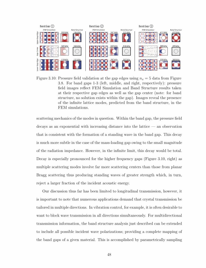
Figure 3.10: Pressure field validation at the gap edges using nx = 5 data from Figure3.8. For band gaps 1-3 (left, middle, and right, respectively): pressurefield images reflect FEM Simulation and Band Structure results takenat their respective gap edges as well as the gap center (note: for bandstructure, no solution exists within the gap). Images reveal the presenceof the infinite lattice modes, predicted from the band structure, in theFEM simulations.
scattering mechanics of the modes in question. Within the band gap, the pressure field
decays as an exponential with increasing distance into the lattice — an observation
that is consistent with the formation of a standing wave in the band gap. This decay
is much more subtle in the case of the mass-loading gap owing to the small magnitude
of the radiation impedance. However, in the infinite limit, this decay would be total.
Decay is especially pronounced for the higher frequency gaps (Figure 3.10, right) as
multiple scattering modes involve far more scattering centers than those from planar
Bragg scattering thus producing standing waves of greater strength which, in turn,
reject a larger fraction of the incident acoustic energy.
Our discussion thus far has been limited to longitudinal transmission, however, it
is important to note that numerous applications demand that crystal transmission be
tailored in multiple directions. In vibration control, for example, it is often desirable to
want to block wave transmission in all directions simultaneously. For multidirectional
transmission information, the band structure analysis just described can be extended
to include all possible incident wave polarizations; providing a complete mapping of
the band gaps of a given material. This is accomplished by parametrically sampling
48
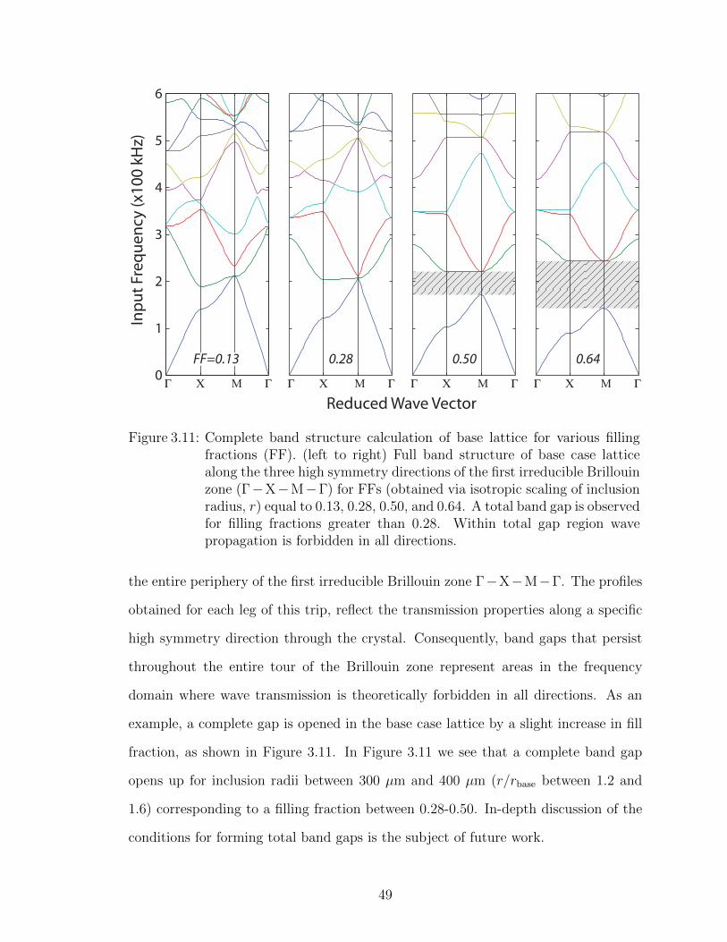
Γ Χ M Γ Γ Χ M ΓΓ Χ M ΓΓ Χ M Γ0
1
2
3
4
5
6
0.28 0.50 0.64
Inpu
t Fre
quen
cy (x
100
kHz)
Reduced Wave Vector
FF=0.13
Figure 3.11: Complete band structure calculation of base lattice for various fillingfractions (FF). (left to right) Full band structure of base case latticealong the three high symmetry directions of the first irreducible Brillouinzone (Γ−X−M−Γ) for FFs (obtained via isotropic scaling of inclusionradius, r) equal to 0.13, 0.28, 0.50, and 0.64. A total band gap is observedfor filling fractions greater than 0.28. Within total gap region wavepropagation is forbidden in all directions.
the entire periphery of the first irreducible Brillouin zone Γ−X−M−Γ. The profiles
obtained for each leg of this trip, reflect the transmission properties along a specific
high symmetry direction through the crystal. Consequently, band gaps that persist
throughout the entire tour of the Brillouin zone represent areas in the frequency
domain where wave transmission is theoretically forbidden in all directions. As an
example, a complete gap is opened in the base case lattice by a slight increase in fill
fraction, as shown in Figure 3.11. In Figure 3.11 we see that a complete band gap
opens up for inclusion radii between 300 µm and 400 µm (r/rbase between 1.2 and
1.6) corresponding to a filling fraction between 0.28-0.50. In-depth discussion of the
conditions for forming total band gaps is the subject of future work.
49

3.4 Conclusion
Numerous geometric properties of 2D phononic crystals have been examined with
regard to their associated influence on the emergence and evolution of band gaps.
While two-dimensional phononic crystals have previously been studied, the treat-
ment of lattice geometry has thus far been cursory. FEM simulations were used to
generate transmission profiles for finite crystal arrays confined within theoretically
infinite ducts. The results illustrate the richness of the influence of lattice geometry
on the properties of transmission band gaps. A 1D TMM approach was employed
as an intuitively tractable analytical model for approximating the transmission char-
acteristics of the 2D crystals while also minimizing computational demands. It was
found that transmission profiles of the 2D simulations were well reproduced by intro-
duction of a set of effective waveguide dimensions. Profiles of the 2D crystals were
compared with calculated band structure, i.e., transmission in the infinite limit. Band
structure results agreed remarkably well with the transmission characteristics of the
duct-confined systems despite the finite scale of the simulated crystals.
50

CHAPTER IV
ADVANCES IN MODULAR MICROFLUIDIC
CONSTRUCTION
4.1 Introduction
Microfluidics devices are particularly advantageous for biological analysis [25, 58–
61] and high-throughput screening [62–64]. However, despite their financial and
scientific benefits (e.g. experimental parallelization, reduced reagent consumption,
short analysis times, portability, the ability to create bio-mimetic structures [65]),
widespread adoption of such devices in the research community has yet to occur.
One reason for this may be that a significant gap typically exists between the pro-
ducers of microfluidic technologies (mainly engineers) and end users, the majority
of which reside in the life sciences. The high cost and expertise often required to
fabricate custom microfluidic devices [66], it would seem, remains a sufficient deter-
rent to those researchers who might otherwise benefit from the technology. As such,
the development of technologies which enable custom microfluidic fabrication without
demanding substantial investment and/or expertise will go a long way toward closing
this gap.
Interestingly, the field of microfluidics is divided into two, essentially independent,
branches of technology development. One branch is industrial, and is devoted to
51
the development of lab-on-a-chip technologies for the purposes of commercialization.
Devices in this category typically focus on the transformation of multiple laboratory
steps into unit operations contained on disposable/swappable micro-device. These
devices then interface with a permanent master unit that handles fluidic actuation
and data collection. The other branch, which is more relevant to this work, resides in
academia and is primarily concerned with the development and use of microfluidics as
either workhorse research tools or as custom devices for highly specific applications.
Not surprisingly, many developers in this branch concerned with the utility rather
than marketability of microfluidic devices and
A number of researchers have proposed simpler fabrication methods [11–14, 67]
aimed at the elimination of costly and time consuming clean-room lithography. To
replace the conventional chrome photomask, for example, Duffy et al. introduced
the use of high-resolution transparencies [11]. Glennon et al. went further, moving
to direct printing of the lithographic mold — laser toner, in this case, serving as
the fluidic structures [12]. This approach is limiting however, as it only allows for
a maximum channel height of ≈10 µm which is problematic for some biological ap-
plications [67]. Others went further still, creating more topologically diverse molds
using solid object printers (SOP) [14]. But SOP is not ideal due to the substantial
cost of the equipment an its generally limited resolution (≈250 µm minimum feature
size). A clever technique employing direct printing on shrinkable thermoplastics was
recently proposed by Grimes et al. and is potentially useful for fabricating channels
in the range of 50-100 µm [13].
Modular architectures utilizing fluidic breadboards and prefabricated microfluidic
components are a popular development of late [16–18]. This approach, more than
any other, is amenable to ubiquitous distribution among research scientists as pre-
fabricated components would allow for standardization and point of use customiza-
tion. However, the use of a breadboard places inherent limitations on the flexibility of
52

such systems. Recently, Rhee and Burns developed a modular microfluidic assembly
block (MAB) platform [15] using pre-fabricated PDMS blocks. With this approach,
non-expert users could assemble fully-customizable microfluidic devices within min-
utes at the point of use. Furthermore, this approach did not require the use of a
complex breadboard interface.
Here we report on an advanced MAB concept employing PDMS blocks with as-
sorted channel geometries that are linked together and bonded to form fully functional
microfluidic devices (see Figure 4.1). Specifically, we introduce: (1) flexible ice-cube
tray casting to replace rigid SU-8 molds, greatly increasing the speed and ease with
which MABs can be fabricated and extracted, (2) the use of pre-coated substrates
and the methodology for their preparation utilizing inexpensive “off-the-shelf” tools,
and (3) a new block design featuring self-aligning structures as well as small radii on
the sealing faces of the male MABs for improved sealing at block junctions. The com-
bination of these advances allows rapid assembly of MABs into a variety of working
devices.
4.2 Materials and Methods
4.2.1 SU-8 Master Mold Preparation
MAB fabrication begins with preparation of master mold structures in SU-8.
These precursor SU-8 master molds were constructed in two steps using standard
photolithography. First, a thin (50-100 µm) layer of fluidic structures comprised of
assorted channel geometries was deposited. Second, thicker (250-1200 µm) structures
which define the walls of the MABs were added. The fluidic layer of the mold was
prepared by spin-casting either SU-8 2025 or SU-8 2035 (MicroChem Corp.) onto
bare 4 inch silicon wafers (500 µm thick) to a desired feature height, typically 80 µm.
Once coated, wafers were allowed to rest for 5 minutes before being transferred to a
53

Figure 4.1: The MAB concept. (a) Schematic representation of the assorted male andfemale MABs used in this work (b) A selection of pre-fabricated MABsprior to (left) and following (right) assembly and bonding. (c) Photographof actual MAB device, of identical construction, during a flow test.
54

level hotplate with a perforated cover and soft-baked for 5 minutes at 65 ◦C followed
by 20 minutes at 95 ◦C, ramping the temperature slowly (2 ◦C/min) to ensure smooth
solvent evolution. After cooling to room temperature, edge beads were removed by
gentle application of a clean room swab soaked in EBR-PG (MicroChem Corp.) with
wafers rotating at 500 RPM. De-beaded wafers were exposed on a contact aligner for
≈25 seconds (500-750 mJ/cm2) against a chrome photomask containing the fluidic
features (see Appendix A Figure A.1a) and allowed to rest for 30 minutes before un-
dergoing a post-exposure bake at 65 ◦C for 3 minutes and 10 minutes at 95 ◦C, again
gently ramping the temperature up and down on a hotplate with a perforated cover.
Once cool, wafers were submersion developed in fresh SU-8 Developer (MicroChem
Corp.), rinsed with IPA, and gently blown dry with compressed air or nitrogen.
Mold walls were prepared in a similar fashion, by spin-casting SU-8 2150 (Mi-
croChem Corp.) directly on top of the fluidic structures just described. Spun films
were covered and allowed to settle on a level surface for approximately 1 hour prior
to soft baking. Trapped bubbles in the resist film that were not liberated during the
rest period were coaxed out of the resist film by heating the wafers for approximately
30 minutes in a solvent-rich environment, i.e., completely covered with a glass dish,
to 65 ◦C. Any remaining bubbles were ruptured manually, replacing the glass dish as
necessary to maintain a solvent-rich air/resist interface. Bubble-free resist films were
subsequently soft-baked at 95 ◦C for approximately 7 hours, again ramping the tem-
perature slowly (2 ◦C/min). Once cool, edge beads were carefully removed using the
procedure described above. Following the soft-bake, wafers were aligned to a chrome
photo-mask patterned with the assembly block walls (Appendix A Figure A.1b) and
exposed. For example, an approximately 500 µm film was exposed for 90 seconds or
2300 mJ/cm2. Wafers were then allowed to rest for 30 minutes prior to undergoing a
low temperature post-exposure bake at 55 ◦C for 2 hours, during which time, a very
slow temperature ramp (1 ◦C/min) is utilized in order to minimize internal stress in
55

the final SU-8 structures [68]. After returning to room temperature, the wafers were
submersion developed for 20-30 minutes (depending on the film thickness), rinsed
with IPA, DI water, then allowed to air dry. Molds were subsequently treated with
O2 plasma and placed in an evacuated vessel along with 20 µL of tridecafluoro-1,1,2,2-
tetrahydrooctyl-1-trichlorosilane for 1 hour. A complete schematic representation of
SU-8 master mold preparation is shown in Appendix A Figure A.2.
4.2.2 Mold Replication in Silicone
Durable and flexible silicone replicates of the SU-8 master molds were fabri-
cated using a commercially available, low-viscosity liquid silicone rubber (CopyFlex
- MYOM, Cincinnati, OH) with a working time of approximately 4 hours. Com-
pleted SU-8 master molds were placed in a casting tray and encapsulated with the
two-component CopyFlex R© liquid silicone, prepared according to the manufacturer’s
recommendations. To ensure an accurate and void-free mold impression, the encapsu-
lated molds were subjected to 30 inch. vac. Mercury for 10-20 minutes. Subsequently,
the molds were baked in the oven at approximately 80 ◦C for 2 hours. Once cool, a
perfect positive (+) impression of the master mold is recovered by gently peeling
away the cured silicone, which releases effortlessly as a result of the silane treatment
discussed above. Failure to silanize the SU-8 precursor resulted in unwanted bonding
and often destruction of the master mold. The negative (-) impression of the SU-8
structures was recovered by a repetition of the same silanization and encapsulation
procedure just described ending with the silanization of the recovered negative.
4.2.3 Assembly Block Casting
Large populations of defect-free MABs were rapidly produced by casting ≈9:1
(base:catalyst, by weight) mixture of PDMS (Sylgard 184, Dow Corning) within the
recessed wells of the final silanized silicone molds. The casting procedure was per-
56

formed by applying an amount of PDMS sufficient to cover the entire mold to a
height just above the mold surface. The covered mold was then placed in 30 inch.
vac. Mercury for ≈5 minutes or until a quiescent, bubble-free, PDMS film was ob-
served. Then using a standard razor blade and applying a modest amount of pressure,
excess PDMS was slowly drawn off the mold surface. The best results were achieved
by sweeping the razor blade diagonally across the mold furrows with the blade angled
slightly in the direction of travel (≈30-45 ◦). Due to slight compression of the silicone
surface during this procedure (necessary to minimize residual PDMS at the top of
the mold walls), it was often necessary to backfill some of the wells. These wells were
easily identifiable in good light due to their concave liquid surfaces. Backfilling of
wells was accomplished by loading ≈200 µL of PDMS into a 1000 µL micropipette
tip, removing the tip from the micropipette and using the semi-filled tip as a capillary
restrained liquid hopper. Once filled, mold was placed in the oven for approximately
1-2 hours at 80 ◦C. Cured MABs were then readily removed by flexure of the mold
and extraction with dull tweezers. Using this procedure, virtually every usable MAB
(wells at the periphery of the mold are often useless as a result of the edge bead
removal) was routinely extracted without damage to either the mold or blocks in a
matter of minutes.
4.2.4 Substrate Preparation
To prepare a given substrate, a liberal amount of PDMS (1:1) was dispensed onto
the glass surface. Then, this liquid was spread into a think film by slowly walking
a jet of compressed air or nitrogen in a steady zigzagging pattern over the entire
length of the substrate with the jet situated at roughly a 30-45◦ angle relative to
the substrate surface. The jet was formed using a simple compressed air gun with
on/off toggle fitted with a 2 mm ID nozzle (≈ 1 cm in length) in conjunction with
a course upstream pressure regulator and gauge. This procedure was repeated until
57

a
b
c
Figure 4.2: SEM images of precursor SU-8 master molds. (a) Mold with ≈250 µmthick walls and 80 x 200 µm fluidic channels. (b) Mold with ≈500 µmthick walls and 80 x 200 µm fluidic channels. (c) Image of mold in (b)illustrating the negative pitch or sidewall irregularity that was typicallyobserved
an advancing liquid front was no longer visible on the substrate surface. For a 2 x 1
inch glass slide, this took approximately 1 minutes. After the thin-film was spread,
substrates were then allowed to rest for 5-10 minutes prior to MAB assembly.
4.2.5 Device Assembly
Devices were assembled in a stepwise fashion, on pre-coated glass substrates, by
linking the MABs necessary to realize a given design using a pair of fine point tweezers.
Scotch tape (3M Corp) was used to remove dust and particulates from the channel
side of the MABs prior to use and a standard stereoscope was used, though was
not required, as a visual aid during the assembly process. Linking of blocks was
greatly facilitated by placing the MABs, insofar as possible, directly in their desired
location. A preferred approach was to lean the connecting end of the MAB on the
relevant block then depress the alignment keys until the channel side of the block made
contact with the liquid film. Once seated, it was typically necessary to press on the
block surface to liberate any air bubbles that may have become trapped. This process
58

was repeated, periodically checking the overall alignment, until the target design was
realized. Following assembly, completed devices were transferred to a 140 ◦C hotplate
to cure for ≈ 5 minutes. Once cooled, PDMS posts for fluidic interfacing were affixed
to inlet/outlet MABs using a straightforward stamp and cure approach or, optionally,
O2 plasma bonding. Leaks, if present, were quickly repaired by simply returning the
device to the 140 ◦C hotplate and applying a very small amount of PDMS (1:1) to
the effected junctions. For high pressure applications or if a more robust device was
desired, bonded MAB assemblies were fully encapsulated in a thick layer of PDMS
(10:1).
4.3 Results and Discussion
4.3.1 SU-8 Fabrication
SU-8 master molds were constructed using a multi-step photolithographic ap-
proach. Completed molds consisted of thin fluidic structures (typically 80 µm), with
a variety of channel designs, and thick walls (typically 250-500 µm) that defined the
periphery of the MABs. Adjustment of channel and wall dimensions were possible
by alteration of spin speed, use of alternate SU-8 formulations, or by the succes-
sive addition of multiple spin and bake cycles [15]. SEM images of two completed
master molds are shown in Figures 4.2a and 4.2b. Final SU-8 structures possessed
very smooth sidewalls with sharply defined boundaries — two features critical to the
quality of inter-block alignment and sealing. A slightly negative or overhanging pitch
to the SU-8 sidewalls (Figure 4.2c) was typically observed regardless of the mold
wall thickness. This phenomenon results from the use of a broadband UV source on
the contact aligner and could be eliminated by installation of a long-pass filter to
block UV transmission below 350 nm. Sidewall overhang manifests itself, in this case,
as V-shaped crevices between adjacent MABs. The consequence of this, depending
59

Figure 4.3: Schematic representation of replication of SU-8 master molds in flexiblesilicone. (a) Pre-cursor master mold constructed from SU-8 on a 4” Siliconwafer. (b) Chemical surface modification of (a) with trichlorosilanes. (c)Encapsulation of (b) with liquid silicone. (d) Positive silicone cast follow-ing release. (e) Chemical surface modification of (d) with trichlorosilanes.(f) Encapsulation of (e) with liquid silicone. (g) Recovery of negative sil-icone cast following release. (h) Chemical surface modification of (g)with trichlorosilanes. (i) Filling of MAB wells with PDMS monomer. (j)Following PDMS polymerization, MAB’s are released by flexure of thesilicone mold. (k) Image of actual 250 µm silicone mold during step (j).(i) Extraction of a male MAB using a pair of blunt tweezers.
upon the severity of the overhang, are inter-block gaps that potentially extend to the
channel floor.
It is worth noting that thick SU-8 processing was made particularly difficult by
the development of high internal stresses in the final cross-linked epoxy. For SU-8
structures thicker than ≈250 µm, it was common to experience — even with careful
preparation — severe cracking, de-lamination, substrate deformation, and resist dis-
tortion. These issues were all but eliminated after implementing a protocol similar to
one developed by Li et al. who used extended soft-bake times, lower post-exposure
bake temperatures, and slow temperature ramping, in order to achieve final SU-8
structures with 70% less internal stress and 50% greater tensile strength [68].
60

4.3.2 Flexible Casting Trays
MAB extraction from rigid SU-8 master structures requires the delicate use of
sharp tools such as syringe needles or razor blades [15]; however, even with great care,
it is difficult to avoid gouging the sidewalls of the SU-8 and/or damaging the MABs
themselves in the process. To address this, we developed a casting approach which
facilitates MAB extraction while also preserving the integrity SU-8 masters. The
approach, illustrated in Figures 4.3a-4.3j, utilizes a low-viscosity liquid silicone rubber
to create near-perfect — some benign surface roughening was observed (see Appendix
A Figure A.3) — replicates of the original SU-8 master structures. Silicone rubber
replicates are highly flexible and durable, allowing for the production of MABs with
greater rapidity and ease without causing damage to costly SU-8 master structures.
Chemical treatment of the silicone replicates with trichlorosilanes was found to yeild a
passivated surface that did not bind to PDMS. MAB extraction, as such, was trivially
performed by flexing the casting tray and extracting the MABs with a pair of dull
tweezers (see Figure 4.3k and 4.3l). With this process, it was common to harvest an
entire tray’s worth of MABs (50 - 60 blocks) with nearly 100% success in only minutes,
and hundreds of MABs within a few hours. An additional benefit to this approach is
that affords other opportunities for potential end users, namely, the option to make
one’s own supply of MABs.
Some thickness variation among extracted MABs was observed. These variations
(> 100 µm in some cases) arose from insufficiently leveled hot plates during the soft-
bake and post exposure bake steps of the lithography. Female MABs were found to
be thicker, on average, than males regardless of master mold thickness ( see Appendix
A Figure A.4). This difference in overall piece thickness reflects the consistent orien-
tation with which the wafers were placed in the hotplates. Note that these variations
did not appear to effect the performance of planar MAB assemblies. However, such
variations would inhibit realization of three-dimensional, multi-layer, MAB devices.
61
Development of multi-layer MAB structures is the subject of ongoing work and will
allow for more advanced microfluidic components such as peristaltic pumps, valves,
and fluidic logic structures [69, 70] to be created in the same manner as a planar
MAB device.
4.3.3 Block Design
Abrupt deviations in channel cross-section and/or flow direction can pose problems
for microfluidic systems by introducing sharp pressure drops and small pockets of
stagnation in the flow. Thus, the fabrication method used should yield devices with
reliable hydraulic diameters. Toward this end, MABs were modified to include jigsaw-
like lock and key (male and female) structures (Figure 4.4a). These structures fix
the relative orientations of neighboring MABs thus ensuring both local and long
range alignment of the fluidic network. The sealing face of the male MABs were also
modified to include very small trapezoidal extensions (henceforth referred to as the
piece convexity) of 0, 2, 5, and 10 µm (see δ, in Figure 4.4a). Alignment and offset
data for numerous MAB junctions at each convexity is shown in Figure 4.4b. Detailed
statistics of channel offset and alignment angle are plotted in Figures 4.4c-4.4f. The
interquartile range of the relative channel offset (α/w), for example, was found to be
±0.06 with a maximum recorded offset of ≈ 0.2. Similarly, the relative channel angle
(θ− 180 ◦) was found to be approximately ±1.0 ◦ with a maximum angle deviation of
3.0-4.0 ◦. Note that channel offset and angle do not appear to be a function of piece
convexity; however, the data for 0 µm convexity displays the tightest range in each
case.
Elimination of inter-block gaps is important to the functionality of completed
MAB devices. To minimize the occurrence of inter-block gaps (mathematically de-
fined as the distance between two blocks at the channel roof) varying amounts of
convexity were added to the sealing face of the male pieces. By incorporation of this
62

a
c d
b
e f
w
male female
-5 -4 -3 -2 -1 0 1 2 3 -5 -4 -3 -2 -1 0 1 2 3
-0.3 -0.2 -0.1 0 0.1 0.2 -0.2 -0.1 0 0.1 0.2
0
2
5
10
Relative Channel Angle ( -180o)
Relative Channel Angle ( -180o)
Conv
exity
(µm
)Co
nvex
ity (µ
m)
Number of MAB Junctions
Num
ber o
f MAB
Junc
tions
Relative Channel Angle ( -180o)
Relative Channel Offset ( /w)
Rela
tive C
hannel O
ffset (
/w)
Rela
tive C
hannel O
ffset (
/w)
0
2
5
10
0
5
10
15
20
25
30
0
5
10
15
20
25
30
35
5
Convexity
Figure 4.4: Channel alignment and offset statistics for a random sampling of MABjunctions with various piece convexities. (a) Schematic illustration ofa MAB junction highlighting relevant parameters: channel width (w),channel offset (α), channel angle (θ), piece convexity (δ). (b) Bulls-eyeplot of relative channel offset (α/w) and relative channel angle (θ− 180◦)for ≥ 20 MABs at each convexity. (c) Box plot of relative channel offsetversus piece convexity. (d) Histogram of (c). (e) Box plot of relativechannel angle versus piece convexity. (f) Histogram of (e).
63

Figure 4.5: Inter-block gaps for a sampling (N ≥ 20 in each case) of bonded MABswith different piece convexity. (a) Histogram of inter-block gap magni-tudes for assembled and bonded MABs of various convexity (four bins:0-5 µm, 5-10 µm, 10-15 µm, and 15-20 µm). (b) Microscope image of a 0µm gap. (c) Microscope image of a 16.7 µm gap.
additional material, it was thought that the sealing faces of two linked MABs would
be held in a state of increased compression, thus decreasing the likelihood of gaps
forming. Moreover it was thought that the presence of these minuscule PDMS cush-
ions would compensate for the V-shaped crevices resulting from the negatively sloping
sidewalls in the master structures mentioned above. Strangely, a sampling of bonded
MAB junctions at each convexity indicates that an increase in convexity results in an
increase in both the frequency and the magnitude of the observed inter-block gaps
(Figure 4.5a). Despite this somewhat counterintuitive result, the vast majority of
sampled junctions (> 80%, regardless of convexity) exhibit inter-block gaps of ≤ 5
µm; moreover, within that group, the fraction of junctions displaying no gaps were
80%, 60%, 56%, and 56% for convexities of 0, 2, 5, and 10 µm, respectively. For
illustrative purposes, a pair of such junctions with 0 µm and 16.7 µm gaps are shown
in Figure 4.5b and 4.5c, respectively.
64

4.3.4 Substrate Preparation
Researchers often take advantage of the native stiction of PDMS in the design
and construction of microfluidic systems. Stiction is problematic, however, when
attempting to precisely position arrays of objects in close proximity to one another.
For MABs, such a scenario is particularly undesirable because poor positioning of
the blocks leads to non-functional devices. As such, we developed a simple means
of preparing glass substrates for MAB assembly by coating them with thin-films of
PDMS monomer. Our thin-films, the thickness of which is tunable over a range of 1-3
µm, serve as a lubricating layer upon which MABs can freely glide, allowing linked
assemblies of MABs to settle into tight low-stress configurations. The thin liquid
films have the added benefit of wicking up into the interstitial spaces between blocks
allowing for covalent lateral linkage of the MABs during the heat cure step.
Preliminary determination of the optimal film thickness was accomplished by per-
forming MAB assembly on a series of spin-coated (1:1) films with thicknesses of 2-22
µm. Note that the MABs used possessed channel depths of 60-80 µm. A film of ≈2
µm (6,000 RPM, 30 seconds) was found to be of sufficient liquidity to allow facile ma-
nipulation of the MABs and capillary wicking of PDMS into the block gaps, but was
thin enough so that the fluidic channels did not readily flood during a routine assem-
bly. However, because the purchase of a spin-coater is likely not feasible for most end
users, numerous “off-the-shelf” methods were explored in an effort to reproduce the
characteristics of the 6,000 RPM spun films. The average thickness and deviation for
films prepared by: spin coater at 6,000 RPM, 40 psi compressed air, hand application
with a clean room wipe, a razor blade drawn over bare glass, and a razor blade drawn
over various etched glass recesses is plotted in Figure 4.6a. Of these methods, the
use of a compressed gas jet was found to be superior, yielding films with a thickness
and deviation comparable to those of the spin-coated benchmark films. Etched glass
recesses, though ultimately effective in producing the target film thickness suffered
65
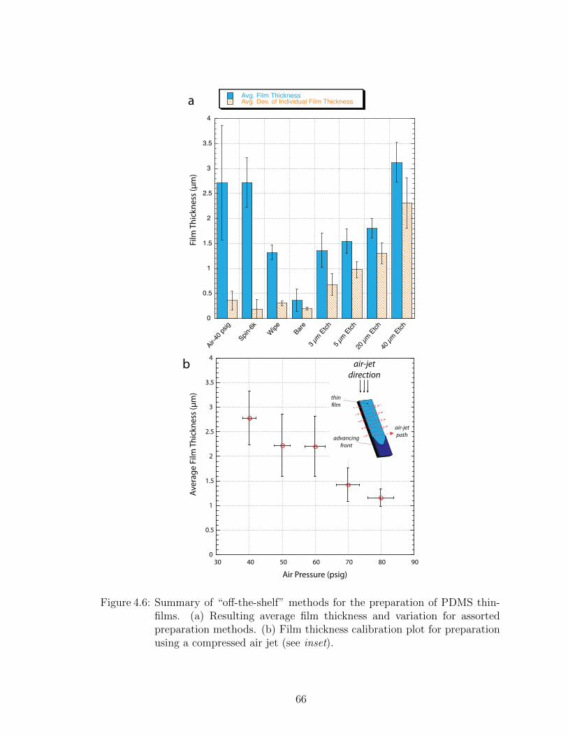
0
0.5
1
1.5
2
2.5
3
3.5
4
Air-40 p
sig
Spin-6k Wipe Bare
3 µm E
tch5 µ
m Etch
20 µm
Etch
40 µm
Etch
Avg. Film ThicknessAvg. Dev. of Individual Film Thickness
Film
Thi
ckne
ss (µ
m)
a
b
0
0.5
1
1.5
2
2.5
3
3.5
4
30 40 50 60 70 80 90
Air Pressure (psig)
Aver
age
Film
Thi
ckne
ss (µ
m)
air-jetdirection
air-jetpathadvancing
front
thin!lm
Figure 4.6: Summary of “off-the-shelf” methods for the preparation of PDMS thin-films. (a) Resulting average film thickness and variation for assortedpreparation methods. (b) Film thickness calibration plot for preparationusing a compressed air jet (see inset).
66
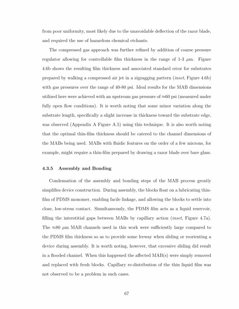
from poor uniformity, most likely due to the unavoidable deflection of the razor blade,
and required the use of hazardous chemical etchants.
The compressed gas approach was further refined by addition of coarse pressure
regulator allowing for controllable film thickness in the range of 1-3 µm. Figure
4.6b shows the resulting film thickness and associated standard error for substrates
prepared by walking a compressed air jet in a zigzagging pattern (inset, Figure 4.6b)
with gas pressures over the range of 40-80 psi. Ideal results for the MAB dimensions
utilized here were achieved with an upstream gas pressure of ≈60 psi (measured under
fully open flow conditions). It is worth noting that some minor variation along the
substrate length, specifically a slight increase in thickness toward the substrate edge,
was observed (Appendix A Figure A.5) using this technique. It is also worth noting
that the optimal thin-film thickness should be catered to the channel dimensions of
the MABs being used. MABs with fluidic features on the order of a few microns, for
example, might require a thin-film prepared by drawing a razor blade over bare glass.
4.3.5 Assembly and Bonding
Condensation of the assembly and bonding steps of the MAB process greatly
simplifies device construction. During assembly, the blocks float on a lubricating thin-
film of PDMS monomer, enabling facile linkage, and allowing the blocks to settle into
close, low-stress contact. Simultaneously, the PDMS film acts as a liquid reservoir,
filling the interstitial gaps between MABs by capillary action (inset, Figure 4.7a).
The ≈80 µm MAB channels used in this work were sufficiently large compared to
the PDMS film thickness so as to provide some leeway when sliding or reorienting a
device during assembly. It is worth noting, however, that excessive sliding did result
in a flooded channel. When this happened the affected MAB(s) were simply removed
and replaced with fresh blocks. Capillary re-distribution of the thin liquid film was
not observed to be a problem in such cases.
67
Figure 4.7: (a) Schematic illustration of an assembled MAB device and detail (inset)of the device cross-section shown by plane No. 1 highlighting the capillarywicking of the liquid film into the inter-block gap. (b) Companion SEMimage of the cross-section defined by plane No. 1 in an actual MABdevice with the same channel geometry. (c) Close-up of the highlightedrectangle in (b) showing the bond which has formed at the MAB junctionwell above the channel roof. (d) Companion SEM of plane No. 2 in(a) showing the vertical bond penetration extending from the substratesurface ≈150 µm.
68

Lateral and surface bonding of MAB assemblages occurs in minutes after place-
ment on a 140 ◦C hotplate. Figures 4.7b-4.7d show SEM cross-sections of some ex-
ample MAB devices following the bonding step. Notice that the block interfaces have
formed a continuum due to the capillary penetration of the PDMS liquid film. When
necessary for high-pressure applications (> 5 psi) or simply when a more robust de-
vice was desired, finished MAB devices were encapsulated in a thick (≈0.5 - 1 cm)
layer of PDMS. The result is a finished device that is virtually indistinguishable to
one produced using conventional soft lithography.
Leaks were occasionally observed during fluidic testing of finished MAB devices
owing to the presence of inter-block gaps, but were easy to fix. When present, leaks
were invariably found to occur at inter-block junctions and always vertically upward
through the V-shaped crevice between pieces. It is important to note that in such
cases the utility of the device was rarely lost. In fact, the repair of leaks was found
to be quick and straightforward. Such a device was simply returned to the 140 ◦C
hotplate and a small amount of PDMS (1:1) was applied on the effected junctions
using a loaded micropipette tip. The polymerization time, given the small amount
of PDMS and the high catalyst ratio, was on the order of a few seconds. Thus, even
relatively large inter-block gaps (≈20 µm) were routinely repairable as the PDMS,
which rapidly fills the inter-block region, polymerizes before any channel flooding
could occur.
4.4 Exemplary Applications of MAB Devices
4.4.1 Chemical Gradient Synthesis
Fine spatial control of chemical gradients is helpful the study of cellular popu-
lations, where it is often desirable to probe for toxicity limits over a wide range of
concentrations. Using a traditional experimental approach, this would require prepa-
69

ration of a series of dilutions and simultaneous monitoring of a number of experiments
in parallel. The same task is made far simpler in a microfluidic system with the aid
of a chemical gradient generator. Such a device produces a spatial concentration gra-
dient spanning the transverse dimension of a given micro-channel and can be finely
tuned by adjusting inlet flow ratios. Using this approach, a continuum of toxicity
data could conceivably be obtained in a single compact experiment.
The layout for a two-component version of such a device constructed from 58
MABs is shown in Figure 4.8a. The finished device, which has been encapsulated
in PDMS for durability, along with gradient data generated by the device across
the path M-M are shown in Figures 4.8b and 4.8c, respectively. Note the long-
range alignment of the fluidic channels and the smooth nearly linear variation in the
generated gradient.
4.4.2 Droplet Generation
Among its many documented applications, microfluidic droplet generation is very
attractive as a means of culturing microbial consortia, where symbiotic nutrient ex-
change between constituent members is poorly understood. In a microfluidic setting,
thousands of uniformly sized droplets containing a probabilistic distribution of un-
known species can easily be generated in seconds. The sequestered droplets could
then be incubated and later screened for symbiotic interactions. This form of high
throughput screening requires narrow tolerances on the sizes of generated droplets as
well as stability of the resulting emulsion.
Construction of such droplet devices is straightforward with MABs. Figure 4.8d
shows an example of a simple flow-focusing droplet generator consisting of 12 standard
MABs and 1 custom droplet collection/cultivation block. Images of the working
device, after additional PDMS encapsulation to reenforce the large thin diaphragm
of the droplet chamber, is shown in Figures 4.8e and 4.8f. A specialty surfactant
70

Figure 4.8: Chemical gradient and droplet generation in MAB devices. (a) Schematicof two component chemical gradient generator constructed from 58 MABs.(b) Image of completed MAB device following additional encapsulation inPDMS. (c) Pixel intensity plot illustrating the sigmoidal variation of thegenerated gradient along the path M-M’ in (b). (d) Schematic of 13 blockflow-focus droplet device. (e) Close-up image of the device in (d) duringoperation illustrating the formation of a water droplet at the flow-focusedjunction (dotted lines are to illustrate channel boundaries). (f) Close-upimage of the device in (d) during operation showing the generation andaccumulation of highly stabilized and uniform droplets in the downstreamchamber (dotted lines are to illustrate channel boundaries).
71

(RainDance Technologies, Inc.) was used to stabilize the generated droplets which
can be packed into the droplet chamber and incubated for greater than 24 hours
without coalescence — a necessary characteristic for in-vitro cultivation.
4.4.3 Total Internal Reflectance Microscopy
Total internal reflectance microscopy (TIR) is an indispensable experimental tech-
nique for studying the dynamics of single fluorophores. For single molecule re-
searchers, particularly in the biological sciences, the most common method for imag-
ing and probing their samples is to simply add them between a microscope slide and
cover glass. Custom micro-channels are often created between these pieces using, for
example, double-sided tape, wax, or Parafilm R©. Later, holes can be drilled with dia-
mond drill bits to allow for fluidic delivery of reagents and buffers. MABs offer a far
more precise and straightforward means of fabricating these custom micro-channels
as blocks with user defined dimensions are very easily assembled at the point-of-
use and afford users options for flow and sample manipulation not possible with the
conventional approach.
To demonstrate the use of MABs for both objective (Figure 4.9a) and prism-based
total internal reflection (TIR) microscopy of small fluorescent nano spheres and sin-
gle molecular fluorophores at or near the PDMS/water interface, single channel MAB
devices were constructed on microscope cover glass (Figure 4.9b). During TIR exci-
tation most microspheres (200 nm in diameter, suspended in a dilute water solution)
were found to be in a state of brownian motion; however, many of the beads were
found adsorbed to the ≈2 µm layer of PDMS at the glass boundary. TIR was readily
apparent by comparing emission of intensely bright — due to their proximity to the
evanescent TIR field — surface-bound beads with those of the freely diffusing beads
(see Figure 4.9c). Adjusting the TIR to allow for epi-illumination of the buffer so-
lution resulted in the beads in solution becoming readily apparent, and the diffusing
72

Figure 4.9: TIR Microscopy using MAB devices. (a) Simplified schematic ofobjective-based TIR microscope operation. (b) Image of 7 block straightchannel MAB device, with attached fluidic inputs, on the TIR microscopestage. (c) Image from objective-TIR excitation experiment illustratingthe contrast in signal strength for surface bound (bright) versus freelydiffusing (dim) 200 nm nanospheres.
bead paths could be seen for long paths of travel as long as they were near the focus
of the microscope. TIR was also verified by measuring the emission from the surface
beads as the TIR angle was adjusted through a series of angles. The results show
excellent promise for the use of MABs in many applications where imaging at the
PDMS/buffer interface is needed. Similar experiments for prism-based TIR were also
performed (data not shown).
73

4.5 Conclusions
The MAB approach presented is a simple and inexpensive alternative to traditional
microfabrication techniques and is aimed at closing the gap between the developers of
microfluidic technologies and the core potential user base in the life sciences. Anyone,
regardless of discipline, can quickly assemble these building blocks into sophisticated
microfluidic devices according to their own designs. In this work we discussed several
advancements to the original MAB concept [15] including: the use of flexible molds
for improved casting and extraction of MABs, the modification of the block design to
include auto-alignment structures, analysis of the effectiveness of added material to
the male structures for improved sealing, and the use of pre-coated substrates for con-
densing the assembly and bonding steps of the process. Exemplary MAB devices were
also presented to illustrate that the technology could be readily applied to a variety of
scientific applications. The MAB platform has no intrinsic limitations on the channel
layouts or block dimensions used. Future users of MABs could work with fabrication
foundries to develop custom sets of blocks to suit their specific needs. Simplified
MAB production using flexible silicone molds affords users the additional option of
producing their own supply of MABs. Optimization of precursor mold lithography
will allow for MABs with highly uniform thickness and perfectly vertical sidewalls.
Perfectly vertical sidewalls could eliminate inter-block gaps, and by extension, the
need to repair leaks. Such improvements would enable the construction of multi-layer
MAB devices with more advanced structures such as pneumatic control and fluidic
logic.
74

CHAPTER V
CONCLUSIONS AND CONTINUING WORK
5.1 Conclusions
The overall aim of this dissertation work was to identify and develop new tech-
nologies for improving the usability of microfluidic tools, with specific emphases on
micro-scale flow control and device fabrication. Our investigation of micro-scale flow
control led us to develop a novel acoustic-based parallel pressure regulation scheme
which was used to coordinate fluid motion within branched channel networks. In
this scheme, an input acoustic signal consisting of one or more embedded frequencies
were converted into a set of independently addressable output pressures via a unique
coupling of resonance cavities and fluidic rectification structures. The device we con-
structed possessed four resonance cavities, each of which were tunable on the range
of 0 - 200 Pa with a control resolution of ≈ 10 Pa. Using this system, we showed that
versatile programmable fluidic manipulation was possible by interfacing the device
with either droplet-based or continuous flow microfluidic systems.
Toward alternative acoustic flow control mechanisms, we conducted a detailed
study of 2D phononic crystal microstructures focusing on transmission band gap
properties related to perturbations in crystal geometry. Our results illustrated the
richness of lattice geometry on the properties of phononic stop bands. In searching
for computationally leaner alternatives to full FEM simulations, we found that 1D
75
waveguides possessing effective dimensions could very accurately reproduce 2D FEM
transmission below, and in the vicinity of, the principle band gap. Finally, we showed
that great insight into the transmission behavior of finite crystals could be gleaned
by analysis in the theoretical infinitely spanning limit.
In order to make microfluidic prototyping more universally accessible to non-
experts, we developed an advanced MAB methodology greatly reducing the time,
cost, and expertise required for microfluidic device construction. We found that
MAB casting and extraction were dramatically improved by replication of the rigid
SU-8 master molds in flexible silicone rubber. Later we discovered that assembly and
bonding steps could be accomplished simultaneously by use of substrates pre-coated
with very thin (≈2 µm) films of PDMS. Furthermore, it was shown that these thin
films could be prepared in a reliable fashion using off-the-shelf methods. Potential
sources of user error during the block assembly process were all but eliminated by
incorporating auto-alignment and sealing structures. Lastly, demonstrations of ex-
emplary MAB devices were performed in order to illustrate the variety of potential
applications in which MABs can be applied.
5.2 Continuing Work
5.2.1 Integrated Acoustic Flow Control
The ultimate goal for the acoustic flow control concept presented in Chapter 2 was
always to integrate the components on-chip. An embedded microfluidic flow control
system possessing the functionality of the prototype macro-system would enable the
operation of a complex device using, in theory, only a single on-chip electrical connec-
tion — the decoding, amplification, and transduction of the signal would, as in the
microsystem, take place on the device itself. Having completed the proof of concept
device, future work should focus on miniaturization of the components and potential
76
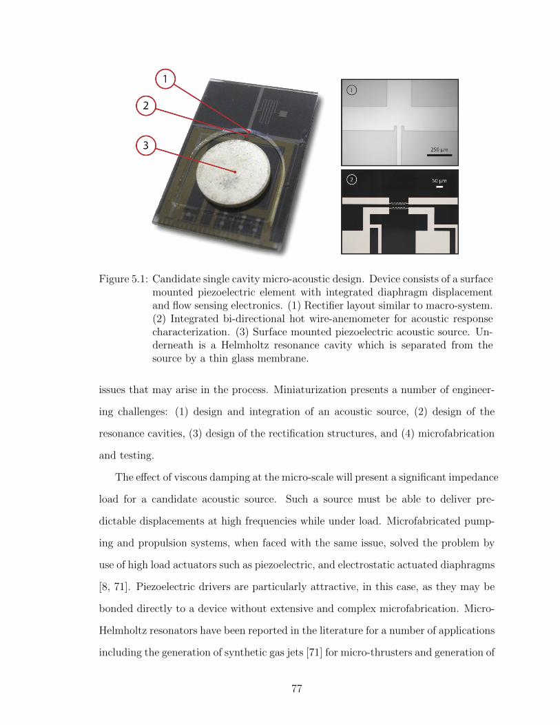
Figure 5.1: Candidate single cavity micro-acoustic design. Device consists of a surfacemounted piezoelectric element with integrated diaphragm displacementand flow sensing electronics. (1) Rectifier layout similar to macro-system.(2) Integrated bi-directional hot wire-anemometer for acoustic responsecharacterization. (3) Surface mounted piezoelectric acoustic source. Un-derneath is a Helmholtz resonance cavity which is separated from thesource by a thin glass membrane.
issues that may arise in the process. Miniaturization presents a number of engineer-
ing challenges: (1) design and integration of an acoustic source, (2) design of the
resonance cavities, (3) design of the rectification structures, and (4) microfabrication
and testing.
The effect of viscous damping at the micro-scale will present a significant impedance
load for a candidate acoustic source. Such a source must be able to deliver pre-
dictable displacements at high frequencies while under load. Microfabricated pump-
ing and propulsion systems, when faced with the same issue, solved the problem by
use of high load actuators such as piezoelectric, and electrostatic actuated diaphragms
[8, 71]. Piezoelectric drivers are particularly attractive, in this case, as they may be
bonded directly to a device without extensive and complex microfabrication. Micro-
Helmholtz resonators have been reported in the literature for a number of applications
including the generation of synthetic gas jets [71] for micro-thrusters and generation of
77

aerial entrained flow. Such systems seem to possess sharp resonance and thus are at-
tractive candidates for the implementation of the acoustic flow control concept where
it is necessary to make step transitions above and below a rectifier threshold pressure,
as we saw in Chapter 2. While other rectifier designs might prove more efficient in
generating a flow asymmetry, a layout similar to the macroscopic system should, in
theory, function at the micro-scale. The only anticipated operational difference would
be an increase in the rectifier threshold pressure due to the reduction in hydraulic
diameter. Also, the larger back-pressures presented in the microsystem may require
incorporation of converging nozzles at the terminus of the rectifier vents, for example,
to introduce an adverse pressure gradient during the compression stroke of the flow
cycle. Figure 5.1 shows a candidate single-cavity micro-acoustic design featuring a
surface-mounted piezoelectric element with integrated flow and diaphragm displace-
ment sensing. Underneath the piezo element, separated by a thin glass membrane, is
a circular Helmholtz cavity with a volume of ≈ 4 µL and estimated resonance of 3.89
kHz computed from the lumped element Helmholtz model found in [57]. Experimen-
tal characterization of this design will include: calibration of flow and strain sensors,
measurement of diaphragm displacement with applied voltage, and mapping of the
acoustic response.
5.2.2 Multi-Layer MABs
The principle question following the advancements to the MAB concept pre-
sented in Chapter 4, is whether or not the MAB approach can be extended to three-
dimensions. In addition to planar fluidic networks multi-layer MABs could have an
enormous impact on the field as they would allow for integration of active fluidic
components such as pumps, valves, and logic structures in addition to planar fluidic
networks. Realization of multi-layer MABs depends chiefly upon minimizing varia-
tions in block thickness. Deviations on the order of 3-5 µm, for example, may in fact
78

!uidiclayer
anchorblock
controllayer
Figure 5.2: Schematic representation of a concept multi-layer MAB device for peri-staltic pumping. The device consists of a fluidic layer (bottom), a controllayer (top), and a doubly-thick anchor block (gray, lower left) for preserv-ing layer to layer alignment.
prove disastrous for multi-layer construction and should be verified experimentally.
Obviously, the most important factor governing the minimum achievable thickness
variation is the uniformity of the MAB walls. Unleveled hotplates, as we saw in Ap-
pendix A, Figure A.4 can produce deviations > 100µm. As such, great care must be
taken to create perfectly level, clean surfaces for the construction of MAB walls.
An additional option, should narrow tolerances prove to be unreachable with
leveling alone, is to replicate the MAB structures in a material such as wax which
can be precision milled. Assuming moderately stress-free SU-8 walls, the base silicon
substrate should provide an extremely flat reference surface enabling an precision
finish end mill to the top surface of the MAB walls to a very high tolerance. Recall
also that a slight negative pitch to the MAB walls was observed owing presumably
to improper filtering of the exposure source. Elimination of this issue figures heavily
in the success of multi-layer MABs and should also be investigated. An example of a
79
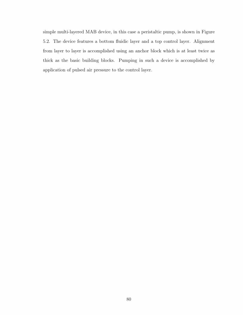
simple multi-layered MAB device, in this case a peristaltic pump, is shown in Figure
5.2. The device features a bottom fluidic layer and a top control layer. Alignment
from layer to layer is accomplished using an anchor block which is at least twice as
thick as the basic building blocks. Pumping in such a device is accomplished by
application of pulsed air pressure to the control layer.
80

APPENDICES
81
APPENDIX A
ADVANCES IN MODULAR MICROFLUIDIC
CONSTRUCTION
A.0.3 SU-8 Master Mold: Processing Notes
An unfortunate consequence of spin casting over the top of existing resist struc-
tures is that during the spin process, small air bubbles may become entrained in
the resist film on the leeward side (i.e., down the gravitational gradient) of the flu-
idic structures. This is particularly true for the thicker resists and tall rectangular
structures employed here. Liberation of trapped air from SU-8 2150 was found, at
times, to be quite challenging. The approach which produced the most consistently
acceptable resist films consisted of heating the coated wafers on a level hotplate in a
solvent rich atmosphere, i.e., fully covered, to 65 ◦C for ≈ 30 minutes. This allows
adequate time for free air bubbles to float to the surface and rupture. Bubbles that
did not rupture on their own were manually ruptured using the sharp corner of a
razor blade or syringe tip. This procedure was repeated as necessary and generally
was found to be effective in removing better than 90% of trapped air. The other
10% were typically bubbles either held tightly to the Silicon surface or in the corners
82

of the existing structures. These remaining few bubbles were removed by carefully
dislodging them, again with the corner of a clean razor blade or syringe tip. The
resist film, still being highly liquified at this stage, quickly settles into a mirror like
surface leaving no trace of a disturbance.
A.0.4 Mold Replication in Silicone: Processing Notes
A slight roughening of the silicone surface was typically observed following the
recovery the negative impression, see Figure A.3. Presumably this is a result of
an adverse reaction at the rubber surface during the caustic silanization step. This
roughening was found to be benign, however, and did not effect the performance
of the resulting MABs. Further investigation is required to definitively identify the
source of the roughening. It is possible, for example, that a simple shortening of
the silanization treatment time would lessen (if not eliminate) the surface roughness
while still providing adequate release characteristics.
83
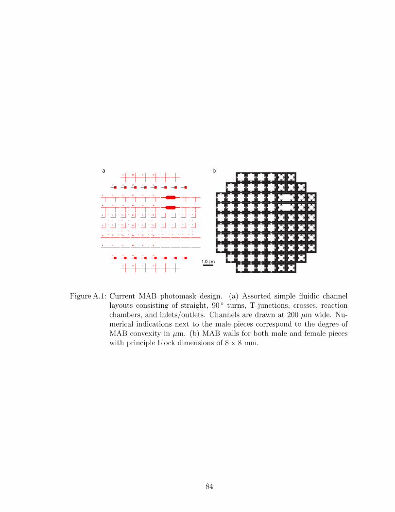
1.0 cm
a b
Figure A.1: Current MAB photomask design. (a) Assorted simple fluidic channellayouts consisting of straight, 90 ◦ turns, T-junctions, crosses, reactionchambers, and inlets/outlets. Channels are drawn at 200 µm wide. Nu-merical indications next to the male pieces correspond to the degree ofMAB convexity in µm. (b) MAB walls for both male and female pieceswith principle block dimensions of 8 x 8 mm.
84
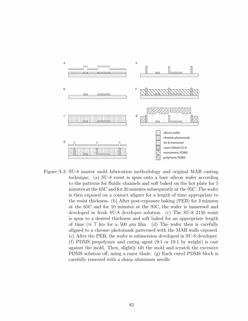
a
b
c
d
e
f
g
silicon waferchrome photomaskSU-8 monomercross-linked SU-8monomeric PDMSpolymeric PDMS
Figure A.2: SU-8 master mold fabrication methodology and original MAB castingtechnique. (a) SU-8 resist is spun onto a bare silicon wafer accordingto the patterns for fluidic channels and soft baked on the hot plate for 5minutes at the 65C and for 20 minutes subsequently at the 95C. The waferis then exposed on a contact aligner for a length of time appropriate tothe resist thickness. (b) After post-exposure baking (PEB) for 3 minutesat the 65C and for 10 minutes at the 95C, the wafer is immersed anddeveloped in fresh SU-8 developer solution. (c) The SU-8 2150 resistis spun to a desired thickness and soft baked for an appropriate lengthof time (≈ 7 hrs for a 500 µm film. (d) The wafer then is carefullyaligned to a chrome photomask patterned with the MAB walls exposed.(e) After the PEB, the wafer is submersion developed in SU-8 developer.(f) PDMS prepolymer and curing agent (9:1 or 10:1 by weight) is castagainst the mold. Then, slightly tilt the mold and scratch the excessivePDMS solution off, using a razor blade. (g) Each cured PDMS block iscarefully removed with a sharp aluminum needle.
85
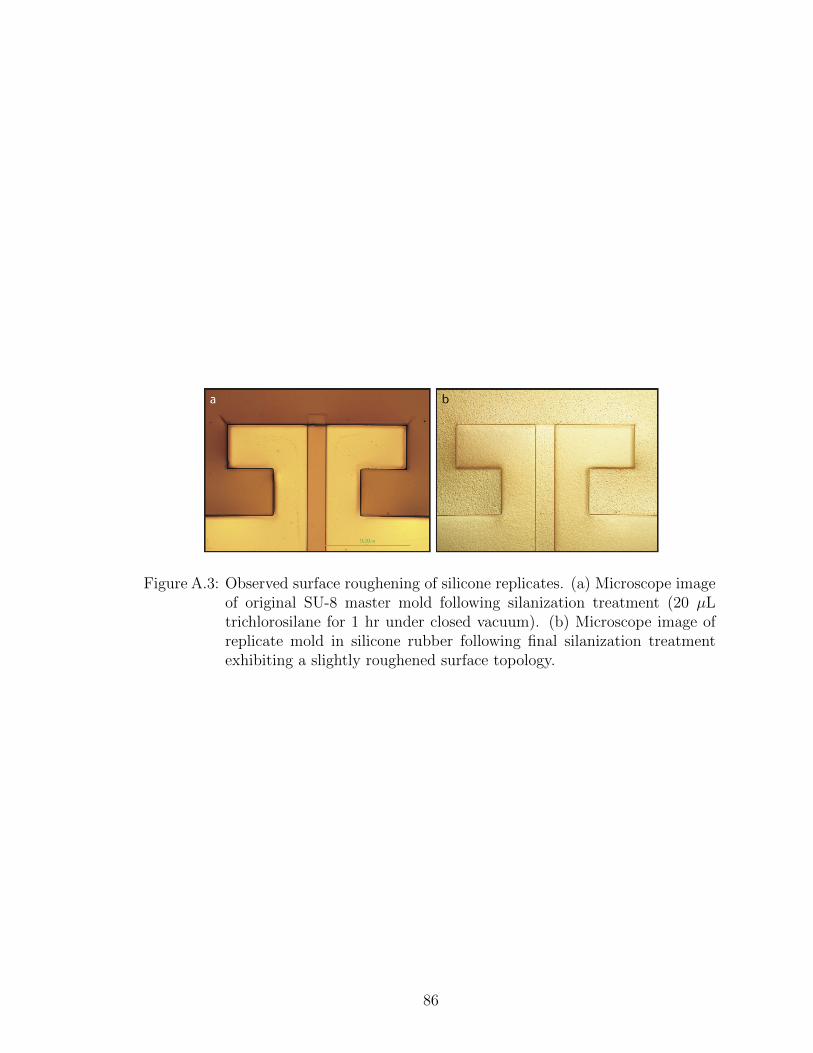
Figure A.3: Observed surface roughening of silicone replicates. (a) Microscope imageof original SU-8 master mold following silanization treatment (20 µLtrichlorosilane for 1 hr under closed vacuum). (b) Microscope image ofreplicate mold in silicone rubber following final silanization treatmentexhibiting a slightly roughened surface topology.
86
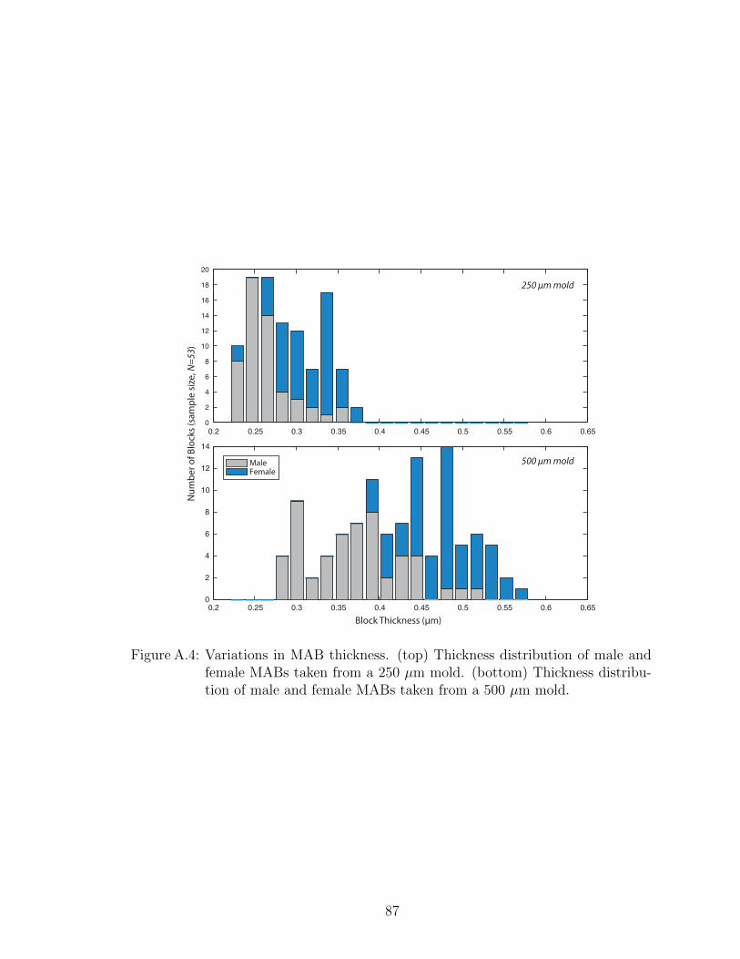
0
2
4
6
8
10
12
14
16
18
20
0.2 0.25 0.3 0.35 0.4 0.45 0.5 0.55 0.6 0.65
0.2 0.25 0.3 0.35 0.4 0.45 0.5 0.55 0.6 0.65
0
2
4
6
8
10
12
14
Block Thickness (µm)
250 µm mold
500 µm mold
Num
ber o
f Blo
cks (
sam
ple
size,
N=5
3)
MaleFemale
Figure A.4: Variations in MAB thickness. (top) Thickness distribution of male andfemale MABs taken from a 250 µm mold. (bottom) Thickness distribu-tion of male and female MABs taken from a 500 µm mold.
87
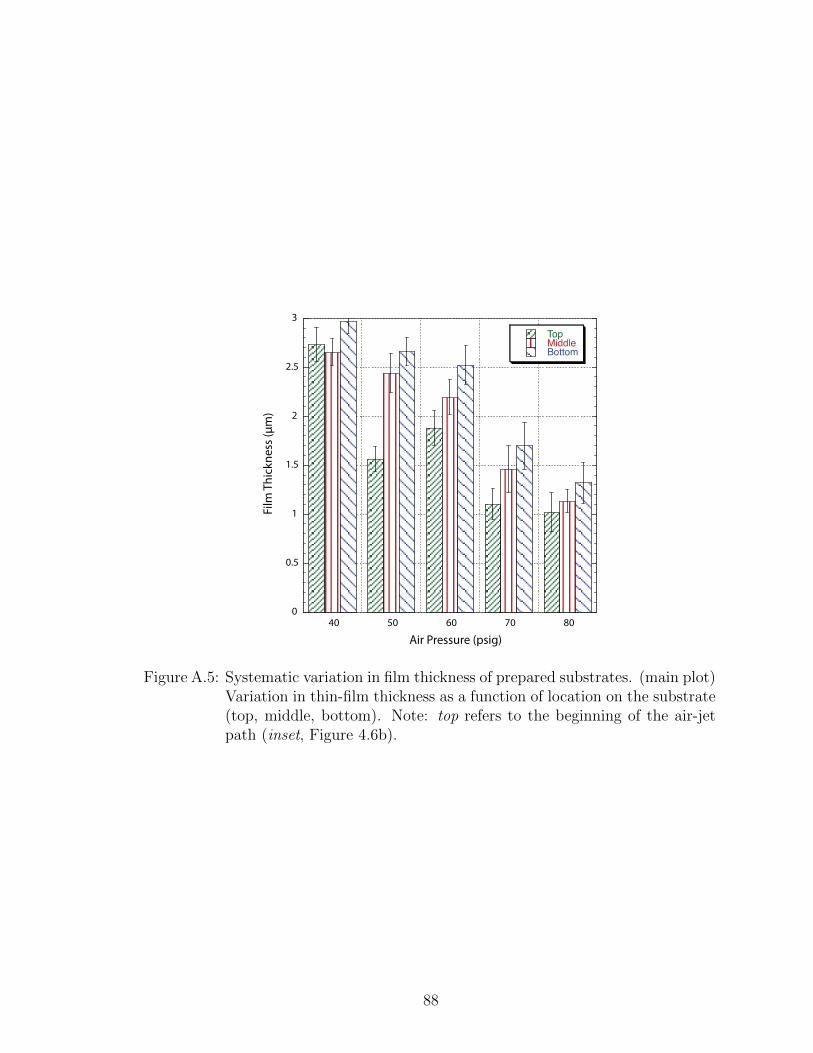
0
0.5
1
1.5
2
2.5
3
40 50 60 70 80
TopMiddleBottom
Air Pressure (psig)
Film
Thi
ckne
ss (µ
m)
Figure A.5: Systematic variation in film thickness of prepared substrates. (main plot)Variation in thin-film thickness as a function of location on the substrate(top, middle, bottom). Note: top refers to the beginning of the air-jetpath (inset, Figure 4.6b).
88

BIBLIOGRAPHY
89
BIBLIOGRAPHY
[1] P.K. Wong, T.H. Wang, J.H. Deval, and C.M. Ho. Electrokinetics in microdevices for biotechnology applications. Mechatronics, IEEE/ASME Transactionson, 9(2):366–376, 2004.
[2] W.E. Morf, O.T. Guenat, and N.F. De Rooij. Partial electroosmotic pumping incomplex capillary systems:: Part 1: Principles and general theoretical approach.Sensors and Actuators B: Chemical, 72(3):266–272, 2001.
[3] J.R. Melcher and M.S. Firebaugh. Traveling-wave bulk electroconvection inducedacross a temperature gradient. Physics of Fluids, 10:1178, 1967.
[4] M. Vallet, M. Vallade, and B. Berge. Limiting phenomena for the spreadingof water on polymer films by electrowetting. The European Physical JournalB-Condensed Matter and Complex Systems, 11(4):583–591, 1999.
[5] D. Juncker, H. Schmid, U. Drechsler, H. Wolf, M. Wolf, B. Michel, N. de Rooij,and E. Delamarche. Autonomous microfluidic capillary system. Anal. Chem,74(24):6139–6144, 2002.
[6] P.D.I. Fletcher, S.J. Haswell, E. Pombo-Villar, B.H. Warrington, P. Watts,S.Y.F. Wong, and X. Zhang. Micro reactors: principles and applications inorganic synthesis. Tetrahedron, 58(24):4735–4757, 2002.
[7] D.J. Laser and J.G. Santiago. A review of micropumps. Journal of microme-chanics and microengineering, 14:R35, 2004.
[8] J.C. Rife, M.I. Bell, J.S. Horwitz, M.N. Kabler, R.C.Y. Auyeung, and W.J.Kim. Miniature valveless ultrasonic pumps and mixers. Sensors & Actuators:A. Physical, 86(1-2):135–140, 2000.
[9] R. Gorkin, J. Park, J. Siegrist, M. Amasia, B.S. Lee, J.M. Park, J. Kim, H. Kim,M. Madou, and Y.K. Cho. Centrifugal microfluidics for biomedical applications.Lab on a Chip, 10(14):1758–1773, 2010.
[10] K. Sritharan, C.J. Strobl, M.F. Schneider, A. Wixforth, and Z. Guttenberg.Acoustic mixing at low Reynolds numbers. Applied Physics Letters, 88:054102,2006.
90
[11] D.C. Duffy, J.C. McDonald, O.J.A. Schueller, and G.M. Whitesides. Rapidprototyping of microfluidic systems in poly (dimethylsiloxane). Anal. Chem,70(23):4974–4984, 1998.
[12] A. Tan, K. Rodgers, J.P. Murrihy, C. O’Mathuna, and J.D. Glennon. Rapidfabrication of microfluidic devices in poly (dimethylsiloxane) by photocopying.Lab on a Chip, 1(1):7–9, 2001.
[13] A. Grimes, D.N. Breslauer, M. Long, J. Pegan, L.P. Lee, and M. Khine. Shrinky-dink microfluidics: rapid generation of deep and rounded patterns. Lab on a Chip,8(1):170–172, 2008.
[14] J.C. McDonald and G.M. Whitesides. Poly (dimethylsiloxane) as a material forfabricating microfluidic devices. Acc. Chem. Res, 35(7):491–499, 2002.
[15] M. Rhee and M.A. Burns. Microfluidic assembly blocks. Lab on a Chip,8(8):1365–1373, 2008.
[16] K.A. Shaikh, K.S. Ryu, E.D. Goluch, J.M. Nam, J. Liu, C.S. Thaxton, T.N.Chiesl, A.E. Barron, Y. Lu, C.A. Mirkin, et al. A modular microfluidic architec-ture for integrated biochemical analysis. Proceedings of the National Academy ofSciences of the United States of America, 102(28):9745, 2005.
[17] P.K. Yuen. SmartBuild–A truly plug-n-play modular microfluidic system. Labon a Chip, 8(8):1374–1378, 2008.
[18] P. Grodzinski, J. Yang, R.H. Liu, and M.D. Ward. A modular microfluidicsystem for cell pre-concentration and genetic sample preparation. BiomedicalMicrodevices, 5(4):303–310, 2003.
[19] G.M. Greenway, S.J. Haswell, D.O. Morgan, V. Skelton, and P. Styring. The useof a novel microreactor for high throughput continuous flow organic synthesis.Sensors & Actuators: B. Chemical, 63(3):153–158, 2000.
[20] E.M. Chan, A.P. Alivisatos, and R.A. Mathies. High-temperature microfluidicsynthesis of CdSe nanocrystals in nanoliter droplets. JACS, 12:17, 2005.
[21] D.C. Pregibon, M. Toner, and P.S. Doyle. Multifunctional encoded particles forhigh-throughput biomolecule analysis. Science, 315(5817):1393, 2007.
[22] B. Zheng, J.D. Tice, and R.F. Ismagilov. Formation of droplets of alternatingcomposition in microfluidic channels and applications to indexing of concentra-tions in droplet-based assays. Analytical Chemistry, 76(17):4977, 2004.
[23] S.Y. Teh, R. Lin, L.H. Hung, and A.P. Lee. Droplet microfluidics. Lab on aChip, 8(2):198–220, 2008.
[24] M.A. Eddings and B.K. Gale. A pdms-based gas permeation pump for on-chipfluid handling in microfluidic devices. Journal of Micromechanics and Micro-engineering, 16(11):2396–2402, 2006.
91

[25] R. Pal, M. Yang, R. Lin, B.N. Johnson, N. Srivastava, S.Z. Razzacki, K.J.Chomistek, D.C. Heldsinger, R.M. Haque, and V.M. et al. Ugaz. An integratedmicrofluidic device for influenza and other genetic analyses. Lab on a Chip,5(10):1024–1032, 2005.
[26] D.S. Chang, S.M. Langelier, and M.A. Burns. An electronic venturi-based pres-sure microregulator. Lab on a Chip, 7(12):1791–1799, 2007.
[27] M.A. Unger, H.P. Chou, T. Thorsen, A. Scherer, and S.R. Quake. Mono-lithic microfabricated valves and pumps by multilayer soft lithography. Science,288(5463):113, 2000.
[28] T. Thorsen, S.J. Maerkl, and S.R. Quake. Microfluidic large-scale integration.Science, 298(5593):580, 2002.
[29] Z. Guttenberg, H. Muller, H. Habermuller, A. Geisbauer, J. Pipper, J. Felbel,M. Kielpinski, J. Scriba, and A. Wixforth. Planar chip device for pcr and hy-bridization with surface acoustic wave pump. Lab on a Chip, 5(3):308–317, 2005.
[30] R.J. Dijkink, J.P. van der Dennen, C.D. Ohl, and A. Prosperetti. The acousticscallop: a bubble-powered actuator. J. Micromech. Microeng, 16:1653–9, 2006.
[31] F. Petersson, L. Aberg, A.M. Sward-Nilsson, and T. Laurell. Free flowacoustophoresis: Microfluidic-based mode of particle and cell separation. An-alytical Chemistry, 79(14):5117–5123, 2007.
[32] L. Puskar, R. Tuckermann, T. Frosch, J. Popp, V. Ly, D. McNaughton, and B.R.Wood. Raman acoustic levitation spectroscopy of red blood cells and plasmodiumfalciparum trophozoites. Lab on a Chip, 7(9):1125–1131, 2007.
[33] J. Lighthill. Acoustic streaming. (Institute of Acoustics, Spring Meeting, Cam-bridge, England, Apr. 6, 1978.) Journal of Sound and Vibration, 61, 1978.
[34] S.W. Schneider, S. Nuschele, A. Wixforth, C. Gorzelanny, A. Alexander-Katz,R.R. Netz, and M.F. Schneider. Shear-induced unfolding triggers adhesion ofvon Willebrand factor fibers. Proceedings of the National Academy of Sciences,104(19):7899, 2007.
[35] A. Groisman and S.R. Quake. A microfluidic rectifier: anisotropic flow resistanceat low reynolds numbers. Physical Review Letters, 92(9):94501, 2004.
[36] V. Tesar. Configurations of fluidic actuators for generating hybrid-synthetic jets.Sensors & Actuators: A. Physical, 138(2):394–403, 2007.
[37] J.V. Sanchez-Perez, D. Caballero, R. Martinez-Sala, C. Rubio, J. Sanchez-Dehesa, F. Meseguer, J. Llinares, and F. Galvez. Sound attenuation by a two-dimensional array of rigid cylinders. Physical Review Letters, 80(24):5325–5328,1998.
92

[38] J. Wen, G. Wang, D. Yu, H. Zhao, and Y. Liu. Theoretical and experimentalinvestigation of flexural wave propagation in straight beams with periodic struc-tures: Application to a vibration isolation structure. Journal of Applied Physics,97:114907, 2005.
[39] J.O. Vasseur, P.A. Deymier, A. Khelif, P. Lambin, B. Djafari-Rouhani,A. Akjouj, L. Dobrzynski, N. Fettouhi, and J. Zemmouri. Phononic crystalwith low filling fraction and absolute acoustic band gap in the audible frequencyrange: A theoretical and experimental study. Physical Review E, 65(5):56608,2002.
[40] M.H. Lu, C. Zhang, L. Feng, J. Zhao, Y.F. Chen, Y.W. Mao, J. Zi, Y.Y. Zhu,S.N. Zhu, and N.B. Ming. Negative birefraction of acoustic waves in a soniccrystal. Nature Materials, 6(10):744–748, 2007.
[41] M. Ambati, N. Fang, C. Sun, and X. Zhang. Surface resonant states and super-lensing in acoustic metamaterials. Physical Review B, 75(19):195447, 2007.
[42] M.F. Su, R.H. Olsson III, Z.C. Leseman, and I. El-Kady. Realization of aphononic crystal operating at gigahertz frequencies. Applied Physics Letters,96:053111, 2010.
[43] M. Torres, F.R. Montero de Espinosa, and J.L. Aragon. Ultrasonic wedges forelastic wave bending and splitting without requiring a full band gap. Physicalreview letters, 86(19):4282–4285, 2001.
[44] A. Khelif, A. Choujaa, S. Benchabane, B. Djafari-Rouhani, and V. Laude. Guid-ing and bending of acoustic waves in highly confined phononic crystal waveguides.Applied Physics Letters, 84:4400, 2004.
[45] P.D.C. King and T.J. Cox. Acoustic band gaps in periodically and quasiperiod-ically modulated waveguides. Journal of Applied Physics, 102:014902, 2007.
[46] Y. Pennec, B. Djafari-Rouhani, J.O. Vasseur, A. Khelif, and P.A. Deymier.Tunable filtering and demultiplexing in phononic crystals with hollow cylinders.Physical Review E, 69(4):46608, 2004.
[47] C.J. Rupp, M.L. Dunn, and K. Maute. Switchable phononic wave filtering,guiding, harvesting, and actuating in polarization-patterned piezoelectric solids.Applied Physics Letters, 96:111902, 2010.
[48] R.H.O.I. El-Kady. Microfabricated phononic crystal devices and applications.Measurement Science and Technology, 20(1):2002, 2009.
[49] Z. Liu, X. Zhang, Y. Mao, Y.Y. Zhu, Z. Yang, C.T. Chan, and P. Sheng. Locallyresonant sonic materials. Science, 289(5485):1734, 2000.
93

[50] W.M. Robertson and J.F. Rudy III. Measurement of acoustic stop bands in two-dimensional periodic scattering arrays. The Journal of the Acoustical Society ofAmerica, 104:694, 1998.
[51] T. Gorishnyy, C.K. Ullal, M. Maldovan, G. Fytas, and E.L. Thomas. Hypersonicphononic crystals. Physical review letters, 94(11):115501, 2005.
[52] R.H. Olsson III, I.F. El-Kady, M.F. Su, M.R. Tuck, and J.G. Fleming. Micro-fabricated VHF acoustic crystals and waveguides. Sensors and Actuators A:Physical, 145:87–93, 2008.
[53] N.K. Kuo, C. Zuo, and G. Piazza. Microscale inverse acoustic band gap structurein aluminum nitride. Applied Physics Letters, 95:093501, 2009.
[54] R. Wei, B. Wu, C. He, and H. Zhao. Phononic band structure in a two-dimensional hybrid triangular graphite lattice. Physica B: Condensed Matter,2009.
[55] E.N. Economou and M.M. Sigalas. Classical wave propagation in periodic struc-tures: Cermet versus network topology. Physical Review B, 48(18):13434–13438,1993.
[56] Y.Z. Wang, F.M. Li, W.H. Huang, and Y.S. Wang. Effects of inclusion shapeson the band gaps in two-dimensional piezoelectric phononic crystals. Journal ofPhysics: Condensed Matter, 19:496204, 2007.
[57] L.E. Kinsler, A.R. Frey, A.B. Coppens, and J.V. Sanders. Fundamentals ofacoustics. Wiley, 1999.
[58] J. El-Ali, P.K. Sorger, and K.F. Jensen. Cells on chips. Nature, 442(7101):403–411, 2006.
[59] M.A. Burns. Everyone’s a (future) chemist. Science, 296(5574):1818–1819, 2002.
[60] D.R. Meldrum and M.R. Holl. Microfluidics: Microscale bioanalytical systems.Science, 297(5584):1197, 2002.
[61] M.A. Burns, B.N. Johnson, S.N. Brahmasandra, K. Handique, J.R. Webster,M. Krishnan, T.S. Sammarco, P.M. Man, D. Jones, and D. et al. Heldsinger. Anintegrated nanoliter dna analysis device. Science, 282(5388):484, 1998.
[62] J.J. Agresti, E. Antipov, A.R. Abate, K. Ahn, A.C. Rowat, J.C. Baret, M. Mar-quez, A.M. Klibanov, A.D. Griffiths, and D.A. Weitz. Ultrahigh-throughputscreening in drop-based microfluidics for directed evolution. Proceedings of theNational Academy of Sciences, 107(9):4004, 2010.
[63] P.J. Hung, P.J. Lee, P. Sabounchi, R. Lin, and L.P. Lee. Continuous perfusionmicrofluidic cell culture array for high-throughput cell-based assays. Biotechnol-ogy and bioengineering, 89(1):1–8, 2005.
94
[64] M.A. McClain, C.T. Culbertson, S.C. Jacobson, N.L. Allbritton, C.E. Sims, andJ.M. Ramsey. Microfluidic devices for the high-throughput chemical analysis ofcells. Anal. Chem, 75(21):5646–5655, 2003.
[65] D. Huh, B.D. Matthews, A. Mammoto, M. Montoya-Zavala, H.Y. Hsin, andD.E. Ingber. Reconstituting organ-level lung functions on a chip. Science,328(5986):1662, 2010.
[66] G.M. Whitesides. The origins and the future of microfluidics. Nature,442(7101):368–373, 2006.
[67] A. Liu, F. He, K. Wang, T. Zhou, Y. Lu, and X. Xia. Rapid method for design andfabrication of passive micromixers in microfluidic devices using a direct-printingprocess. Lab on a Chip, 5(9):974–978, 2005.
[68] B. Li, M. Liu, and Q. Chen. Low-stress ultra-thick SU-8 UV photolithographyprocess for MEMS. Journal of Microlithography, Microfabrication, and Microsys-tems, 4:043008, 2005.
[69] M. Rhee and M.A. Burns. Microfluidic pneumatic logic circuits and digitalpneumatic microprocessors for integrated microfluidic systems. Lab on a Chip,9(21):3131, 2009.
[70] B. Mosadegh, C.H. Kuo, Y.C. Tung, Y. Torisawa, T. Bersano-Begey, H. Tavana,and S. Takayama. Integrated elastomeric components for autonomous regula-tion of sequential and oscillatory flow switching in microfluidic devices. NaturePhysics, 6(6):433–437, 2010.
[71] T.K.A. Chou, K. Najafi, M.O. Muller, L.P. Bernal, and P.D. Washabaugh. Char-acterization of micromachined acoustic ejector and its applications. In MicroElectro Mechanical Systems, 2002. The Fifteenth IEEE International Conferenceon, pages 264–267. IEEE, 2002.
95