activity report - bibsys · activity report july 2007 ... my personal introduction to particle...
TRANSCRIPT

Activity Report
July 2007 - August 2008
European Organisation for Nuclear Research(CERN) 13 Month Placement
Author:
Jo Inge Buskenesmail @ joinge.net
January 8, 2009
French Conseil Européen pour la
Recherche Nucléaire
Supervisor:
Hans Muller
Hans.Muller @ cern.ch
Gjøvik University College
Supervisor:
Are Strandlie
are.strandlie @ hig.no
Created with LATEX

"Imagination is more important than knowledge"
Albert Einstein
Abstract
I attended the technical student program at CERN (The European Organization for NuclearResearch) from July 2007 to August 2008. More specically, I worked with the PHOS (ALICEPhoton Spectrometer) detector, which is one of the sub-detectors in ALICE (A Large IonCollider Experiment). With this report I will try to describe in essence the various activitiesI was involved in and present them in a step-by-step approach. The following topics will becovered:
• The building blocks of our world. My personal introduction to particle physics.
• General description of CERN, LHC (Large Hadron Collider), ALICE and PHOS.
• Digital design on the TRU (Trigger Region Unit). Card description and design conceptanalysis.
• Digital design on the TOR (Trigger OR). Design concept analysis.
• Writing C++ utilities for the RCUs. Description and analysis of oine control utilityand TRU register scanner.
• Appendixes which mainly contains information about my experiences working on digitaldesign in Linux, how to interface the electronics through embedded devices (calledDCS cards, Detector Control System), and how to communicate with the TRU designthrough dedicated registers. The goal here is to provide hints and tips that might comein handy for people aiming to resume my work.
I assume that the reader possesses basic knowledge regarding electronics and digital circuits.However, most of the introductory material should be easy to understand for anyone inter-ested. I will try to refrain myself from including any code in this document, and ratherexplain principles with extensive use of graphics. If the reader wants the actual lines of code,look up how to get it in 1.8 (Additional Resources). I strive to keep my code well commentedand self-explanatory, and should complement the report when more details are desired.
All gures and pictures in this report are to be considered the result of my own work unlessotherwise noted. This applies also for written material, where the sources of my knowledgewill be mentioned and can be looked up in the bibliography.
Jo Inge Buskenes Hans Muller
I hereby assure that every eort has beenmade in order to provide an accurate andcredible report.
I have read this report and can verifythat the contents of this report seemscredible.
Page I

Contents
Abstract I
Contents II
1 Introduction 1
1.1 Particle Physics 101 . . . . . . . . . . . . . . . . . . . . . . . . . . . . . . . . 21.2 The Missing Pieces . . . . . . . . . . . . . . . . . . . . . . . . . . . . . . . . . 31.3 CERN . . . . . . . . . . . . . . . . . . . . . . . . . . . . . . . . . . . . . . . . 41.4 LHC . . . . . . . . . . . . . . . . . . . . . . . . . . . . . . . . . . . . . . . . . 51.5 ALICE . . . . . . . . . . . . . . . . . . . . . . . . . . . . . . . . . . . . . . . . 7
1.5.1 The Trigger System . . . . . . . . . . . . . . . . . . . . . . . . . . . . 81.6 PHOS . . . . . . . . . . . . . . . . . . . . . . . . . . . . . . . . . . . . . . . . 91.7 Report Structure . . . . . . . . . . . . . . . . . . . . . . . . . . . . . . . . . . 111.8 Additional Resources . . . . . . . . . . . . . . . . . . . . . . . . . . . . . . . . 13
2 Trigger Region Unit 14
2.1 Introduction . . . . . . . . . . . . . . . . . . . . . . . . . . . . . . . . . . . . . 152.1.1 Technical Data . . . . . . . . . . . . . . . . . . . . . . . . . . . . . . . 172.1.2 Virtex 2 Pro Resources . . . . . . . . . . . . . . . . . . . . . . . . . . . 18
2.1.2.1 Rocket IO Blocks . . . . . . . . . . . . . . . . . . . . . . . . 182.1.2.2 PowerPC Blocks . . . . . . . . . . . . . . . . . . . . . . . . . 182.1.2.3 Multiplier Blocks . . . . . . . . . . . . . . . . . . . . . . . . . 182.1.2.4 Congurable Logic Blocks (CLB) . . . . . . . . . . . . . . . . 192.1.2.5 Digital Clock Managers . . . . . . . . . . . . . . . . . . . . . 212.1.2.6 Block Select RAM . . . . . . . . . . . . . . . . . . . . . . . . 222.1.2.7 Input and Output Buers . . . . . . . . . . . . . . . . . . . . 22
2.1.3 History . . . . . . . . . . . . . . . . . . . . . . . . . . . . . . . . . . . 232.2 Digital Design . . . . . . . . . . . . . . . . . . . . . . . . . . . . . . . . . . . . 24
2.2.1 Code Buildup . . . . . . . . . . . . . . . . . . . . . . . . . . . . . . . . 242.2.2 General Design Changes . . . . . . . . . . . . . . . . . . . . . . . . . . 262.2.3 Managing Clocks . . . . . . . . . . . . . . . . . . . . . . . . . . . . . . 272.2.4 ADC Communication . . . . . . . . . . . . . . . . . . . . . . . . . . . 29
2.2.4.1 Motivation . . . . . . . . . . . . . . . . . . . . . . . . . . . . 292.2.4.2 Communication Protocol . . . . . . . . . . . . . . . . . . . . 302.2.4.3 Conclusion . . . . . . . . . . . . . . . . . . . . . . . . . . . . 30
2.2.5 ADC Data Synchronisation . . . . . . . . . . . . . . . . . . . . . . . . 312.2.5.1 Motivation . . . . . . . . . . . . . . . . . . . . . . . . . . . . 312.2.5.2 Problem Breakdown . . . . . . . . . . . . . . . . . . . . . . . 332.2.5.3 Discovering Impedance Mismatch . . . . . . . . . . . . . . . 342.2.5.4 Conclusion . . . . . . . . . . . . . . . . . . . . . . . . . . . . 36
2.2.6 Deserialiser . . . . . . . . . . . . . . . . . . . . . . . . . . . . . . . . . 37
Page II
Contents
2.2.6.1 Motivation . . . . . . . . . . . . . . . . . . . . . . . . . . . . 372.2.6.2 Design Introduction . . . . . . . . . . . . . . . . . . . . . . . 382.2.6.3 Input Stage - Sorting the Bits . . . . . . . . . . . . . . . . . 382.2.6.4 Output Stage - Phase Correction . . . . . . . . . . . . . . . . 392.2.6.5 Resource Utilisation . . . . . . . . . . . . . . . . . . . . . . . 412.2.6.6 Running Into Problems . . . . . . . . . . . . . . . . . . . . . 422.2.6.7 Conclusion . . . . . . . . . . . . . . . . . . . . . . . . . . . . 43
2.2.7 Level0 Trigger Calculation . . . . . . . . . . . . . . . . . . . . . . . . . 462.2.7.1 Motivation . . . . . . . . . . . . . . . . . . . . . . . . . . . . 472.2.7.2 Design Changes . . . . . . . . . . . . . . . . . . . . . . . . . 472.2.7.3 Conclusion . . . . . . . . . . . . . . . . . . . . . . . . . . . . 48
2.2.8 TOR Communication . . . . . . . . . . . . . . . . . . . . . . . . . . . 502.2.8.1 Motivation . . . . . . . . . . . . . . . . . . . . . . . . . . . . 502.2.8.2 Timing . . . . . . . . . . . . . . . . . . . . . . . . . . . . . . 512.2.8.3 Data Transmission . . . . . . . . . . . . . . . . . . . . . . . . 522.2.8.4 Command Exchange . . . . . . . . . . . . . . . . . . . . . . . 542.2.8.5 Conclusion . . . . . . . . . . . . . . . . . . . . . . . . . . . . 54
2.2.9 Testbench . . . . . . . . . . . . . . . . . . . . . . . . . . . . . . . . . . 552.3 Conclusion . . . . . . . . . . . . . . . . . . . . . . . . . . . . . . . . . . . . . . 56
3 TriggerOR 57
3.1 TOR Pin-out Mapping . . . . . . . . . . . . . . . . . . . . . . . . . . . . . . . 583.1.1 Motivation . . . . . . . . . . . . . . . . . . . . . . . . . . . . . . . . . 583.1.2 Verication . . . . . . . . . . . . . . . . . . . . . . . . . . . . . . . . . 583.1.3 Conclusion . . . . . . . . . . . . . . . . . . . . . . . . . . . . . . . . . 58
3.2 Stabilising LVDS Inputs . . . . . . . . . . . . . . . . . . . . . . . . . . . . . . 593.2.1 Motivation . . . . . . . . . . . . . . . . . . . . . . . . . . . . . . . . . 593.2.2 Investigation . . . . . . . . . . . . . . . . . . . . . . . . . . . . . . . . 593.2.3 Conclusion . . . . . . . . . . . . . . . . . . . . . . . . . . . . . . . . . 59
3.3 Digital Design . . . . . . . . . . . . . . . . . . . . . . . . . . . . . . . . . . . . 603.3.1 Motivation . . . . . . . . . . . . . . . . . . . . . . . . . . . . . . . . . 603.3.2 Operation . . . . . . . . . . . . . . . . . . . . . . . . . . . . . . . . . . 603.3.3 Conclusion . . . . . . . . . . . . . . . . . . . . . . . . . . . . . . . . . 61
4 Readout Control Unit 62
4.1 Motivation . . . . . . . . . . . . . . . . . . . . . . . . . . . . . . . . . . . . . . 624.2 Compiling the Source Code . . . . . . . . . . . . . . . . . . . . . . . . . . . . 634.3 Preparing the DCS Cards . . . . . . . . . . . . . . . . . . . . . . . . . . . . . 634.4 PHOS Oine Control Utility . . . . . . . . . . . . . . . . . . . . . . . . . . . 64
4.4.1 Motivation . . . . . . . . . . . . . . . . . . . . . . . . . . . . . . . . . 644.4.2 Features And Usage . . . . . . . . . . . . . . . . . . . . . . . . . . . . 65
4.4.2.1 Summary . . . . . . . . . . . . . . . . . . . . . . . . . . . . . 654.4.2.2 PreCompilation Options . . . . . . . . . . . . . . . . . . . . . 654.4.2.3 Settings File . . . . . . . . . . . . . . . . . . . . . . . . . . . 664.4.2.4 When Executed . . . . . . . . . . . . . . . . . . . . . . . . . 66
Page III

Contents
4.4.2.5 The Menu . . . . . . . . . . . . . . . . . . . . . . . . . . . . . 674.4.3 Conclusion . . . . . . . . . . . . . . . . . . . . . . . . . . . . . . . . . 68
4.5 TRU Register Scanner . . . . . . . . . . . . . . . . . . . . . . . . . . . . . . . 694.5.1 Motivation . . . . . . . . . . . . . . . . . . . . . . . . . . . . . . . . . 694.5.2 Features And Usage . . . . . . . . . . . . . . . . . . . . . . . . . . . . 70
4.5.2.1 PreCompilation Options . . . . . . . . . . . . . . . . . . . . . 704.5.2.2 Settings File . . . . . . . . . . . . . . . . . . . . . . . . . . . 704.5.2.3 When Executed . . . . . . . . . . . . . . . . . . . . . . . . . 714.5.2.4 Results . . . . . . . . . . . . . . . . . . . . . . . . . . . . . . 71
4.5.3 Conclusion . . . . . . . . . . . . . . . . . . . . . . . . . . . . . . . . . 72
5 Conclusion 73
A Other Activites 77
A.1 Why Linux? . . . . . . . . . . . . . . . . . . . . . . . . . . . . . . . . . . . . . 78A.2 Software . . . . . . . . . . . . . . . . . . . . . . . . . . . . . . . . . . . . . . . 79
A.2.1 Xilinx ISE . . . . . . . . . . . . . . . . . . . . . . . . . . . . . . . . . . 80A.2.2 iMPACT . . . . . . . . . . . . . . . . . . . . . . . . . . . . . . . . . . 81A.2.3 ChipScope . . . . . . . . . . . . . . . . . . . . . . . . . . . . . . . . . . 83A.2.4 ModelSim . . . . . . . . . . . . . . . . . . . . . . . . . . . . . . . . . . 84A.2.5 Synplify . . . . . . . . . . . . . . . . . . . . . . . . . . . . . . . . . . . 86
A.3 Creating Backups . . . . . . . . . . . . . . . . . . . . . . . . . . . . . . . . . . 87A.4 DCS Interfacing . . . . . . . . . . . . . . . . . . . . . . . . . . . . . . . . . . . 88
A.4.1 Via Ethernet . . . . . . . . . . . . . . . . . . . . . . . . . . . . . . . . 88A.4.2 Via Serial Line . . . . . . . . . . . . . . . . . . . . . . . . . . . . . . . 89A.4.3 Set Up NFS Shares . . . . . . . . . . . . . . . . . . . . . . . . . . . . . 89A.4.4 Connecting to DCS in ALICE . . . . . . . . . . . . . . . . . . . . . . . 90
A.5 RJ45 Standard . . . . . . . . . . . . . . . . . . . . . . . . . . . . . . . . . . . 90A.6 Adjusting the TRU ADC Clocks . . . . . . . . . . . . . . . . . . . . . . . . . 92A.7 FEE CSP Mapping . . . . . . . . . . . . . . . . . . . . . . . . . . . . . . . . . 93
B Chronograms 94
C TRU Communication 98
C.1 Reading from the TRU . . . . . . . . . . . . . . . . . . . . . . . . . . . . . . . 99C.2 Writing to the TRU . . . . . . . . . . . . . . . . . . . . . . . . . . . . . . . . 100C.3 Register List . . . . . . . . . . . . . . . . . . . . . . . . . . . . . . . . . . . . 101
D TRU Logic Utilisation 106
D.1 Old Design . . . . . . . . . . . . . . . . . . . . . . . . . . . . . . . . . . . . . 107D.2 New Design . . . . . . . . . . . . . . . . . . . . . . . . . . . . . . . . . . . . . 108
E Fascinating Facts 109
List of Tables 110
Page IV

Contents
List of Figures 111
Bibliography 118
Glossary 124
Page V

. . . the recipe for everything . . .
. . . hidden dimensions . . .
. . . the God particle . . .
. . . antimatter . . .
. . . dark matter . . .
. . . dark energy . . .
Interested, anyone? 1Introduction
Have you ever looked up to the skies wondering what role you play in the big scheme ofthings? What you were actually looking at, and what a miracle it seems to be that the worldas we know it exists at all? And has it ever occurred to you that through us, the universe isin fact aware of itself? How come this marvel ever came to be?
Fig. 1.1 - What crazy scheme are we involved in? [imgEAS]
By studying how the Universe behaves, it quickly becomes apparent that the further we goback in time the simpler the Universe was. This is how we will proceed; by travelling backin time as far as our knowledge can take us, I will give you a insight about what we alreadyknow about the building blocks of our world. Then I will move on to something even moreinteresting; what we do not know. And as you might suspect, there is a place where severalof these questions might be answered very soon. Keep tuned for more information!
Page 1

1.1. Particle Physics 101
. . . Where nature laws does not apply, but are created. . .
Atom
Electron
Nucleus
Proton
u
u d
Molecule
Matter
Neutron
Quarks
Fig. 1.2 - The Building Blocksof matter [docCERN]
1.1 Particle Physics 101
The most commonly accepted theory we have as to how itall started is called the big bang, and refers a massive explo-sion that occurred 13.7 billion years ago sourcing an immenselyenergy-rich substance which was later bound to form the uni-verse as we know it. Our knowledge goes back as far as to a fewmillionth of a second after the blast. Then the substance hadcooled enough for the particles known as quarks, bosons andleptons to form.
Quarks are particles of matter, and make up protons, neutronsand a large number of lesser-known particles. Bosons are carri-ers of force, representing - respectively - the photon, carrier ofelectromagnetism; Z and W+/W− bosons, carrier of the weakforce; gluons, carrier of the strong force; and the yet to be ob-served Higgs boson, a particle suspected responsible for imbu-ing other particles with mass1. Leptons are particles immuneto strong forces; the most famous being the electron.
The strong force acts on gluons and quarks and ultimatelymakes up matter, the weak force changes particles and atomsfrom one type to another (nuclear reactions), and electromag-netism acts on electrically charged particles. The bosons have aeeting existence as they only exist whilst carrying informationfrom one matter particle to another.
Now, let us go from crash course in particle physics to the unknown!
1Why is gravity not mentioned? See 1.2 (paragraph 4).
Page 2

1.2. The Missing Pieces
1.2 The Missing Pieces
Did you know that the Sun contains enough matter to fuel this solarsystem with energy forbillions of years to come? What does this mean? Matter must be some conned form ofenergy? What is the mechanisms behind this phenomena? How come energy have so manyfaces (this is one of the questions the ALICE experiment seek to nd the answer to - see[docALICE])?
When scientists started to research the subatomic realm they discovered that all particles hadan antiparticle, a counterpart with opposite electric charge. For every particle they created,an antiparticle was created. The conditions under which they were created are expected to bemore or less the same as straight after Big Bang, so it is reasonable to think that there was anequal amount of matter and antimatter back then. Finally, if a particle and its antiparticleever comes in contact with each other they will both be completely annihilated. Good thingthat did not happen you might think. Yes, but why is this? And where is all the antimattertoday?
There are billions of stars in our galaxy, and there are billions of galaxies in the Universe.These contain everything that we know, such as stars and planets. However, astronomersand physicists have found that all of this only accounts for roughly 4% of the total Universe!The remaining part consists of dark matter (26%) and dark energy (70%). Dark matter areinvisible, but are proven to be there because of the huge gravitational elds it sets up.Dark energy is a mysterious substance that seems to be associated with the vacuum in space.It is perfectly distributed both in space and time, and causes the Universe to expand in anever increasing pace. However, what this dark stu actually is remains a mystery.
You may have noticed when we talked about bosons that gravity was not included. This isbecause the most widely recognised model for particle physics today - the Standard Model- does not explain how gravity ts into the picture. However, there is a model that alsoincludes gravity - namely the String Theory. The only problem is, it also implies that inaddition to the 4 known dimensions (space+time) there must also be 6 additional spatialdimensions! They are said to be curled up and so small that we can not see them. Thequestion is how small they are, and can their existence ever be proven? And, if they exist,would it be possible to move between these dimensions?
And nally, we mentioned gravity. What is that? Any idea why matter has mass? Did youknow that the the weight of a proton is 100 times that of the sum of the weight of the particlesit is composed of? Where does all the remaining mass come from? Another particle? Indeed,this is what the scientists believe. They call it the Higgs particle, the God particle, but itremains to be observed.
So, what is next? [ 2 ]
2Based on [intCHP, Science I All left side pages ], [intHBU].
Page 3

1.3. CERN
. . . The Coolest Place in the Universe. . .
Fig. 1.3 - The CERN Globe [imgCGL]
1.3 CERN
CERN (The European Organisationfor Nuclear Research) is located onthe Franco-Swiss boarder not far fromGeneva. It was founded in 1954 by ahandful of pioneers 3 aiming to sharethe cost related to nuclear physics facili-ties and unite European scientists. Sincethen it has grown to become one of theworld's largest and most respected cen-tres for scientic research. It is run by 20European member states4, but 35 non-member countries are also involved inthe programs in various ways. There arearound 2500 people currently employedhere, and in addition there are around 580 universities and institutes representing 85 dier-ent nationalities that use CERNs facilities. Roughly half of the worlds particle physicistscome to CERN for their research.
The work done here has brought forth 5 Nobel Prizes, groundbreaking new knowledge aboutthe inner workings of our world and the birth of the World Wide Web! Furthermore thetechnology developed here can be applied in other elds more relevant to our daily lives, forexample in medical equipment better capable of keeping us healthy. All of this ts very wellwith the CERN philosophy:
Fig. 1.4 - Some Citations from the CERNWeb Page [intCHP] [sofPPT]
• Leading the research into the fundamentals ofour Universe.
• Advancing the frontiers of technology.• Bringing nations worldwide together throughscience.
• Educating the scientists of tomorrow.
So what is really going on here? Take a look at someof the citations in g. 1.4 and make a wild guess.They are from the CERN webpage. What is in theair, or maybe, in the ground?
[ 5 ]
3Raoul Dautry (France), Pierre Auger (France), Lew Kowarski (France), Eduardo Amaldi (Italy), NielsBohr (Denmark) et al.
4Norway is one of the member states.5Based on [intCHP, About us I All left side pages ].
Page 4

1.4. LHC
. . . One Ring to Rule them All. . .1.4 LHC
Fig. 1.5 - The Large Hadron Collider Complex [intPRESS, Custom Tags]
Take a look at g. 1.5 and you will see a plane photo of CERN and its surroundings. In theupper left corner you can see lake Geneva, and in the right corner you can catch a glimpse ofthe Geneva airport. The CERN main site is located just under the illustration of the ATLAS(A Toroidal LHCApparatus) detector, with the southern part of the site sticking out from theupper right corner of the mentioned illustration. The white circles indicates the location ofvarious particle accelerator tunnels, the biggest one is called the The Large Hadron Collider(LHC).
The LHC is - as mentioned - a huge circular particle accelerator situated 50-150m under-ground. It measures 27 km in circumference, and along with its detectors represents thelargest scientic instrument ever made by human kind. The aim is to accelerate particlesup to very high speeds and produce head-on collisions such that they decompose into morefundamental particles. While quite a few have been found (some were mentioned in 1.1),there are probably more to be detected. The LHC is a lean and mean particle hunt machine- the biggest one to date. Particles, beware.
Page 5

1.4. LHC
LINAC 2
Gran Sasso
North Area
LINAC 3Ions
East Area
TI2TI8
TT41TT40
CTF3
TT2
TT10
TT60
e–
ALICE
ATLAS
LHCb
CMS
CNGS
neutrinos
neutrons
pp
SPS
ISOLDEBOOSTERAD
LEIR
n-ToF
LHC
PS
Fig. 1.6 - The Accelerator Complex [docLHCUG]
So what is the crazy looking g. 1.6 representing? Well, when particles are to be acceleratedto energies like at CERN several accelerators must be utilised. The gure shows the networkof accelerators currently present at CERN (I advise the reader not to try to remember all theabbreviations). The particles start their journey in some small accelerators at 99.9998% thespeed of light at an energy of 450GeV (eV = electron-volt). However, while no particle cantravel faster than the speed of light, there is no limit to the amount of energy the particle canattain. When the particles ultimately are being injected into the LHC they are kicked up to99.999999% the speed of light and an energy of 7TeV (the beam now contains enough energyto melt 500kg copper6). You might see that when measuring energy in particle physics, it ismore appropriate to talk about electron-volts than the speed of the particle.
So what happens to particles when they are boosted to higher and higher energies? If weimagine ourselves travelling from the eV-range to the TeV-range, we pass through manydistinct landscapes. In the eV world matter follows the rules of chemistry and solid stateelectronics. Increasing the energy into the MeV-range will provoke nuclear reactions (atomsdecompose into protons and neutrons (electrons are leptons), and we are now talking aboutroughly the energy that matter has attained in the center of the Sun. Moving into the GeV-range we will nd that the matter decomposes even further into bosons, quarks and leptons- as mentioned earlier in 1.1. But what happens when the energy is increased into theTeV-range? Will it help us ll in the blanks in the knowledge of our world as mentioned in1.2? Will we witness completely unknown phenomenas?
A vital part of the puzzle is missing; accelerating particles up to the high energies is to nouse unless we also have the necessary equipment to detect what happens as the particlescollide. From g. 1.5 and g. 1.6 you can see the 4 main detectors on the LHC ring: ATLAS,CMS (The Compact Muon Solenoid Experiment), LHCb (The Large Hadron Collider beautyExperiment) and ALICE. I worked with the latter, so let us have a look at it!
[ 7 ]
6For more fascinating facts, take a look at appendix E.7Based on [docLHCUG], [magSCAM].
Page 6

1.5. ALICE
. . . in Wonderland. . .1.5 ALICE
Y
XZ
NB. Please note that the coordination system in ALICE is right handed.
Fig. 1.7 - The ALICE Detector [imgALIDET, Custom Tags]
The ALICE detector is one of the four large detectors situated in the LHC accelerator ringand is mainly dedicated to the study of heavy-ion collisions. It weighs around 10 000 tons andmeasures 16m high and 26m long. It is composed of 18 subdetectors which together providethe necessary sensory equipment to track and identify the tens of thousands of particle tracksproduced in each heavy-ion collision. In order to get a decent rate of interesting events theALICE detector must be capable of processing 8000 collisions per second (see 1.5.1).
When the particles collide inside the ALICE detector the collision point will be 100 000 timeshotter than the centre of the Sun (around 2000 billion C). What happens to matter at thesetemperatures? The current theory of the strong interaction8 predicts that at these immenseenergies quarks and gluons should no longer be conned inside composite particles, but ratherexist in a free state of matter known as quark-gluon plasma. It is believed that this stateexisted just a few millionth of a second after the Big Bang, so we are sort of looking backin time with the ALICE detector. By studying how the quark-gluon plasma reverts back toa conned state of matter we can expect to nd the answers to how the mechanism behindthe connement work, and to why the weight of a proton is 100 times that of the sum of theweight of the particles it is composed of (see 1.2).
8Called quantum chromodynamics.
Page 7

1.5. ALICE
As previously mentioned bunches of particles collide inside the ALICE detector at a rateof thousands of times per second. For only one of these collisions a vast amount of data isproduced by all the various sensors. We need some sort of lter; some sort of mechanism thatselects only the most interesting collisions (or events, as it is popularly referred to) to sendto the computers for further processing. For this purpose, we lter the data with the use ofa triggersystem consisting of specialised electronics, which - due its huge parallel potential- takes a look at all the data and creates triggers when the data has certain interestingproperties.
1.5.1 The Trigger System
To lter out interesting data from what is not, ALICE utilises a triggersystem designed in 3levels:
• Level 0. This trigger decision must arrive at the Central Trigger Processor (CTP)within a total latency of 1.2µs. With all setup times and cable delays this leaves barely500ns for electronic processing, which means that the decision can only be based on avery simple criteria; like when the signal of a particle is bigger than the average.
• Level 1. If the Level0 decision is validated, the data of the pre-selected particle issearched by more rened algorithms that need a little bit more time. These are mostlybased on physics criterias, like detection of two neighboring particles from a decay ofa single one. Due to the increase of complexity in the trigger calculation, the totaltimeframe is 6.5µs.
• Level 2. Given that the data were accepted by the CTP by both level-0 and level-1from several detectors for the same event, the Level2 trigger is asserted as a requestfor the electronics to start sending data. Later on in the process there might also comeLevel2 messages which rejects or accepts the event based on decisions by the CTP.The timing requirements are even more relaxed here, typically the Level2 trigger comeswithin 90µs and the accept/reject message within 500µs.
Now why am I mentioning this? Well, I was working on the Level0 trigger in one of theALICE subdetectors - the Photon Spectrometer (PHOS, see 1.6). You can see the PHOSdetector in g. 1.7, it is situated on the bottom of the ALICE detector.
[ 9 ]
9Based on [docPHOSUM, page 85], [intIETNS] and [MyMind].
Page 8

1.6. PHOS
. . . Let there be light. . .1.6 PHOS
z
x
64
56
Numberof Crystals
Particles hit the very high density crystals which break down the velocity of the particles and converts the excess energy into light.
The light are converted into electric energy with Avalanche Photo Diodes (APDs) located on the back of the crystals.
Particles
Red lines indicate where the module is split into ”branches”
Electric Pulses
TRU
7 FE
Es
7 F
EEs
TRU
7 FE
Es
7 FE
Es
7 F
EEs
7 FE
Es
7 FE
Es
7 F
EEs
7 FE
Es
7 FE
Es
7 FE
Es
7 FE
Es
7 FE
Es
7 FE
Es
7 FE
Es
7 FE
Es
The electric pulses enter the Front-End Electronics (FEE) cards, and later the Trigger Region Unit (TRU) cards.
RCU
RCU
TRU
TRU
TRU
TRU
TRU
TRU
RCU
RCU
The ReadOut ReadOut Control Units (RCUs) are in charge of communication with FEE and TRU cards, and are also capable of reading out relevant event data.
TORL0 L0
L1
Level 0 triggers are generated by the TRUs. The Trigger OR (TOR) card are responsible for the higher level 1 trigger.
The front and back of the module
Fig. 1.8 - The Basic Buildup of a PHOS Module [sofPPT] [sofPSP]
PHOS is - as the name implies - a detector designed to measure the energy of light particles(photons). As I have tried to illustrate in g. 1.8, a PHOS module is composed of twolayers - a set of crystals and the electronics necessary to process the data coming from thecrystals. Only one PHOS module is depicted, but in the end there will be a total of 5 similarmodules10. For each module there are a total of 3584 (56x64) high density lead-tungstencrystals (PbWO4), each weighing around 1kg. But what are the electronics there for?
The clock in the LHC oscillates at 40MHz, which we have to use when the data are to to bedigitised. If we had sampled the data from the crystals directly we would have had to dealwith a steady stream of 40MHz * 12 [bits/sample] * 3584 [crystals] ≈ 215GB/s permodule, assuming a sample resolution of 12 bits. It should be obvious that there is no waythis amount of data can be processed in realtime in a computer.
The electronics layer is composed of 112 cards called FEEs (Front-End Electronics), 8 TRUs(Trigger Region Unit) and 4 RCUs (Readout Control Unit). Each RCU controls 2 branchesof TRUs and FEEs, where each branch may be considered an independent group of cards.Basically, the function of the electronics layer is fully dened with one branch, but scaledup to 8 in total per PHOS module. Because of this, I will from now on speak about theoperation of a single branch and not the entire module.
10As of today (3.July 2008), there are 1 PHOS module installed in ALICE and two more are being commis-sioned.
Page 9

1.6. PHOS
Z
GTL Data Bus (40 lines)
GTL Control Bus (26 lines)
X
1413121 2 3 4 5 6 7 0 8 9 10 11 FEC #
-y
A particle hits the lead-tungsten crystals .
Attached on the back of the crystals you find a smallchip with Avalanche Photo Diodes (APDs) and Charge
Sensitive Preamplifiers (CSP). The electric signals produced are now sent to the Front-End Electronics (FEEs). Each FEE
receives the signals from 32 CSPs (2 columns of 16 crystals).
NB! Note the axis.
Fig. 1.9 - 1 of the 8 Branches in the Electronics Layer [sofPPT]
Fig. 1.9 shows one of the mentioned branches of cards, consisting of 14 FEE cards and 1TRU. Some of the kinetic energy from the particles produced in a collision in ALICE isconverted into photons in the PHOS crystals. The light is transformed into electric energywith Avalanche Photo Diodes (APDs)11 which is in turn amplied with Charge SensitivePreampliers (CSPs)12. Each FEE is connected to 32 CSPs (2 columns of 16 crystals, forgeometrical positions see tab. C.1, right side). The FEE has two main tasks: (1) Samplingand recording high-gain and low-gain versions of these signals and store them in ALTROchips13 where they can be read out by the RCU via the GTL (Gunning Transceiver Logic)bus, and (2) perform an analog sum of 2x2 patches of crystals (for a total of 8 sums per FEE),shape them to a 100ns semi-Gaussian pulse and send them to the TRU (we call these signalsFastOR) via. LVDS (Low Voltage Dierential Signaling) cables (the red ones in g. 1.9).With this data the TRU can decide whether a Level0 trigger is to be generated.
11The APDs have an eciency of 80% - which means that they eectively converts 80% of the energy in thelight into electric energy!
12The combination of APDs and CSPs in PHOS can sense bunches of photons down as low as 10 photons,which is an extremely low light strength.
13See [docALTRORC] and [docPHOSUM] for more information.
Page 10

1.7. Report Structure
1.7 Report Structure
So what can you expect to nd in the upcoming pages? In order of appearance, these arethe chapters:
• Introduction. The one you are currently reading. I started o with a short intro-duction to particle physics and questions which still remains unanswered. Then I saida few words about CERN, the new particle accelerator LHC, the heavy-ion detectorALICE and one of its subdetectors - PHOS. In the last section of this introduction Iwill explain where additional resources can be found if desired.
• Trigger Region Unit (TRU). Presenting the card with a general description andsome history, before I proceed to discuss digital design where ADC (Analog to DigitalConverter) interfacing and resource utilisation will play a vital role.
• Trigger OR (TOR). After a short description I will proceed to describe some mappingproblems and present a design suggestion for the communication protocol between theTOR and TRUs.
• Readout Control Unit (RCU). Two programs will be described in this chapter,namely the TRU Register Scanner and the Oine Control Utility.
• Conclusion. Some nal thoughts made in the aftermath of my stay.
As you can see, I will order my work into chapters representing the card I was working on(when the general introduction (this one) and conclusion is excluded). These chapters willstart with a small introduction before the various topics are presented. These topics maybe concluded separately, or they might be temporarily concluded while pending the nalconclusion of the chapter. In between the introduction and conclusion the structure willvary depending on what topics are discussed, but the topics discussed in these chapters willgenerally be related to rmware and software design.
Page 11
1.7. Report Structure
During my work I frequently encountered situations where necessary documentation seemedabsent. However, from studying code and asking around I have grown to understand someof these poorly documented aspects. Throughout this report I have tried to blend thisknowledge in between related topics, but some of it just does not well with these chapters.This and other relevant information may be looked up in the appendixes:
• Other Activities. As the title indicates this appendix will act as a container forother activites I was involved in and documented, but was not of such a nature thatthey would blend in well with the main body of this report. Keywords here are Linuxexperiences, BASH scripting for working with backups, DCS interfacing, miscellaneouswork with mapping and phase adjustment tutorial for ADC clocks.
• Chronograms. Some chronograms from ModelSim showing a simulation in progress.
• TRU Communication. Some scripts you may use when trying to write and read theTRU registers via. the RCU will be presented, along with a complete list of the currentTRU registers.
• Fascinating Facts. For those interested.
• TRU Logic Usage. For those interested.
I hope that I succeeded in supplying a document which is digestable, even though it containsquite technical material. The paradox is that whilst you are trying to keep it simple andthe prerequisited knowledge at a minimum, you can not leave out too many details as thiswill render the documentation useless. The question should not be whether it is perfectlyfullling the criteria of some template, but rather if the message was adequately presented.
When writing a report like this it is impossible not to use some abbreviated words, not tomention impractical as often they represent the names of electronic components in our project- and I nd that short names are easier to remember than long names. However, unless theyare thoroughly discussed somewhere locally in the report and not mentioned elsewhere - youwill nd them in the glossary.
This report is best read as a pdf le. This way you get to enjoy bookmark navigation andhyperlinks functionality. However, the colorcodes should make it pretty straightforward toread the paper version aswell. Green coloured words are links to the glossary, red colouredwords are references to the bibliography. In the bibliography you will nd an extensive listof sources and where to get additional information.
This is the extract of my year at CERN, happy reading.
Page 12

1.8. Additional Resources
1.8 Additional Resources
In my report I will describe and discuss several programs and documents. These will bemade available for the reader, either by logging into the server mentioned a few paragraphsdown or by simply clicking the references in this document (if you are reading the electronicversion). If you are reading the paper version you can still nd the right les by simplylooking up the reference-tag in the document bibliography.
I set the document-server up with ftp (File Transfer Protocol)14. To log onto it use thefollowing information:
Site: ftp.joinge.net
Username: iyearn
Password: forcern
You can expect to nd the following information on this server:
• Sourcecode for this document.• Sourcecode for the TRU (most recent).• Sourcecode for the TRU (initial).• Sourcecode for DCS Oine Control Utility.• Sourcecode for TRU Register Scanner.• Sourcecode for TOR (most recent).• Sourcecode for TOR (previous versions).• Datasheets.• PHOS related documents.• ChipScope Project Files (for diagnosis).
Each printed copy of this report will also be accompanied with a CD containing the sameinformation as were present on this server at the date of printing.
14If you are using Windows you can can log onto ftps with Windows Explorer (the lesystem browser), orif you are using Linux you can use e.g. Konqueroror Nautilus - they all oer drag-and-drop functionality
Page 13

2Trigger Region Unit
The Trigger Region Unit (TRU) is the card in charge of calculating the Level0 trigger inPHOS (see 1.5.1 for more details about the triggersystem in ALICE). This is rst triggersignal to be produced in the ALICE detector after a particle collision, and indicates whetherthe data recorded of the event might be worth looking more thoroughly into. In the case ofPHOS, we need to produce a Level0 trigger whenever the energy absorbed by the crystalsexceeds a certain threshold.
It is important that the Level0 signal arrives at the CTP in the ALICE detector no later than800ns prior to the time of a particle collision. Due to propagation delay in the electronics theFastOR (The FastOR pulse is the analog sum of a 2x2 matrix of crystals) signals produced bythe FEE cards arrives at the TRU ≈150ns after impact time. This means that the TRU mustgenerate the Level0 trigger signal in less than 450ns (leaving around 200ns for propagationtime from the TRU to the CTP). This might sound hard, but since the TRU has resourceshighly capable of performing parallel computations it is in fact quite feasible.
The TRU is the card I have spent most of my time with. My work related to the TRU canbe split into two parts:
• Digital design for the Virtex 2 Pro FPGA (Field Programmable Gate Array) presenton the TRU.
• Hardware testing, modications and assembly.
This report will not deal with the latter, as I consider the former far more important. Inorder to provide an gentle start on the topic of digital design I will start this chapter witha general description of the TRU and present some of the key features of the Virtex 2 ProFPGA. In the section dealing with digital design I will describe the parts of the design I wasinvolved in and thoroughly discuss the various considerations that was made along the way.Finally, the chapter will be wrapped up with a conclusion where I will suggest what futurework should be carried out.
Page 14
2.1. Introduction
2.1 Introduction
Z
GTL Control Bus (26 lines)
GTL Data Bus (40 lines)
X
1413121 2 3 4 5 6 7 0 8 9 10 11 FEC #
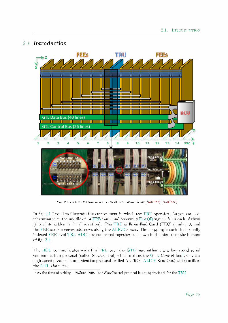
Fig. 2.1 - TRU Position in a Branch of Front-End Cards [sofPPT] [sofGMP]
In g. 2.1 I tried to illustrate the environment in which the TRU operates. As you can see,it is situated in the middle of 14 FEE cards and receives 8 FastOR signals from each of them(the white cables in the illustration). The TRU is Front-End Card (FEC) number 0, andthe FEE cards receives addresses along the ALICE x-axis. The mapping is such that equallyindexed FEEs and TRU ADCs are connected together, as shown in the picture at the bottomof g. 2.1.
The RCU communicates with the TRU over the GTL bus, either via a low speed serialcommunication protocol (called SlowControl) which utilises the GTL Control bus1, or via ahigh speed parallel communication protocol (called ALTRO - ALICE ReadOut) which utilisesthe GTL Data bus.1At the time of writing - 20.June 2008 - the SlowControl protocol is not operational for the TRU.
Page 15
2.1. Introduction
Fig. 2.2 - Front Side View of the Trigger Region Unit (TRU) [sofPSP]
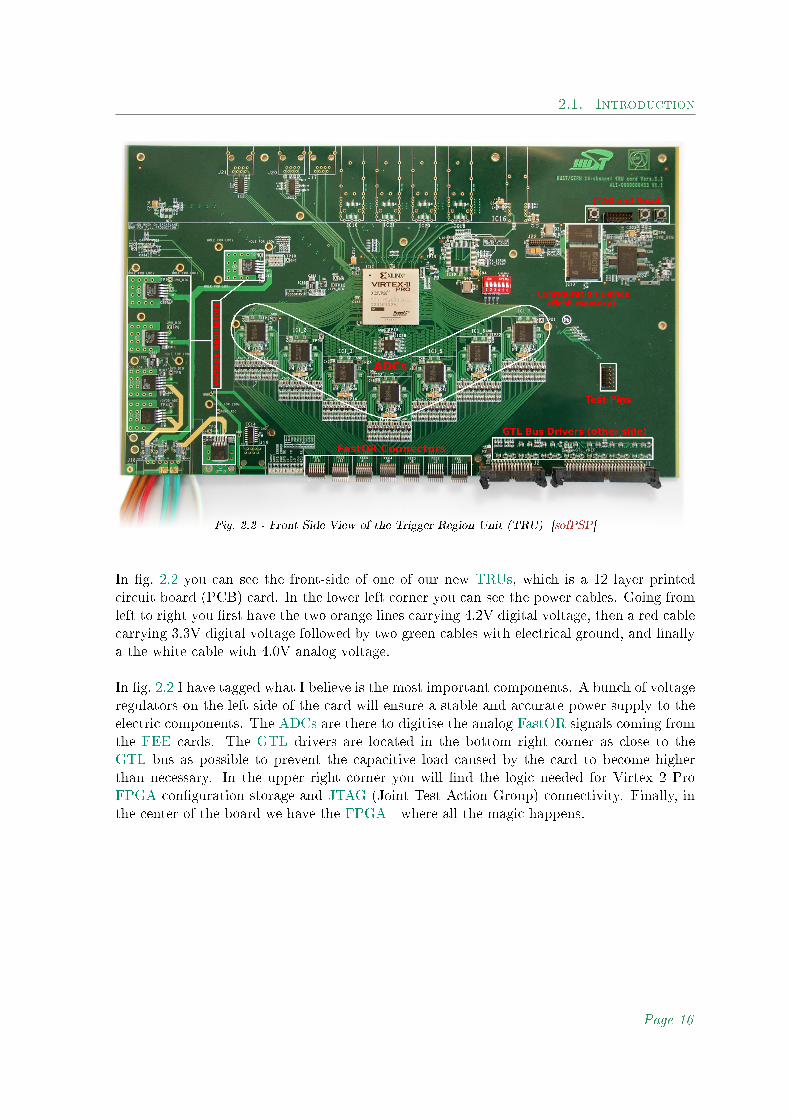
In g. 2.2 you can see the front-side of one of our new TRUs, which is a 12 layer printedcircuit board (PCB) card. In the lower left corner you can see the power cables. Going fromleft to right you rst have the two orange lines carrying 4.2V digital voltage, then a red cablecarrying 3.3V digital voltage followed by two green cables with electrical ground, and nallya the white cable with 4.0V analog voltage.
In g. 2.2 I have tagged what I believe is the most important components. A bunch of voltageregulators on the left side of the card will ensure a stable and accurate power supply to theelectric components. The ADCs are there to digitise the analog FastOR signals coming fromthe FEE cards. The GTL drivers are located in the bottom right corner as close to theGTL bus as possible to prevent the capacitive load caused by the card to become higherthan necessary. In the upper right corner you will nd the logic needed for Virtex 2 ProFPGA conguration storage and JTAG (Joint Test Action Group) connectivity. Finally, inthe center of the board we have the FPGA - where all the magic happens.
Page 16

2.1. Introduction
2.1.1 Technical Data
I believe that a list of components present on the TRU and the links to where you cannd the datasheets might come in handy, so I supply this information for TRU design v1.1[docTRU1.1] (tab. 2.5)2:
Component Type Design Unit DataSheet
Virtex 2 Pro FPGA XC2VP50 IC17 [docV2PDS][docV2PUG]
ADCs ADS5270IPFP IC1_[1,7],IC2_[1,7] [docADC]Congurable Flash Memory XCF32P IC24 [docXCF32P]ProASIC Flash Memory APA075 IC13 [docAPA075]Flash memory MX29LV640DBTI-90G IC12 [docMX29LV]GTL Drivers GTL16612DGG IC3-IC9 [docGTL]Voltage Regulator LT1963A-1.5 Q2 [docVR15V]Voltage Regulator LT1963A-2.5 Q1,Q3 [docVR25V]Voltage Regulator * LTC1844ES5-1.8 REG1 [docVR18V]Voltage Regulator MIC29301-33BU IC33 [docVR33BU]Voltage Regulator MIC29501-33WU IC31 [docVR33WU1]Voltage Regulator MIC20151-33WU IC32 [docVR33WU2]Power Supply Transistor SO2222A Q4,Q5 [docSO2222]Temperature Sensor * MAX6627 IC34 [docMAX6627]Temperature Sensor AD7417 IC22,IC23 [docAD7417]Clock Distribution Chip MPC9109 IC28 [docMPC9109]LVDS Driver ALT_SCLK * SN65LVDS101 IC1 [docLVDS101]LVDS Driver J21,J19 * SN65LVDS31 IC2,IC14 [docLVDS31]LVDS Receiver J20 * SN65LVDS32 IC15 [docLVDS32]MUX/DEMUX ADG774 IC25,IC26,IC27 [docADG774]Transceiver Rocket IO ** V23818-K305-V17 IC16Receiver Rocket IO ** HDMP-1034 IC19Transceiver Rocket IO ** HFBR-5720AL IC10,IC18,IC20,IC21
* Component names from Design Sheet v1.1 [docTRU1.1]. I was not able to verify them.
** Rocket IO components were never installed.
Tab. 2.1 - TRU Components
For my work there is in fact only the two topmost components that we really need to knowa bit about. The FPGA is a pretty complex device that enables us to program the logic thattie all the other components together in an unied way. In the eld of programming suchdevices - digital design - quite a bit of experience is required in order to be able to produceanything with a decent level of quality. A good starting point is to know the specications ofthe FPGA we are working with, so we will take a closer look at the Virtex 2 Pro XC2VP50FPGA in the next subsection.
2Some of the component names may dier from what is specied in the design sheet as these are the actualcomponents installed on the board, visually veried.
Page 17
2.1. Introduction
2.1.2 Virtex 2 Pro Resources
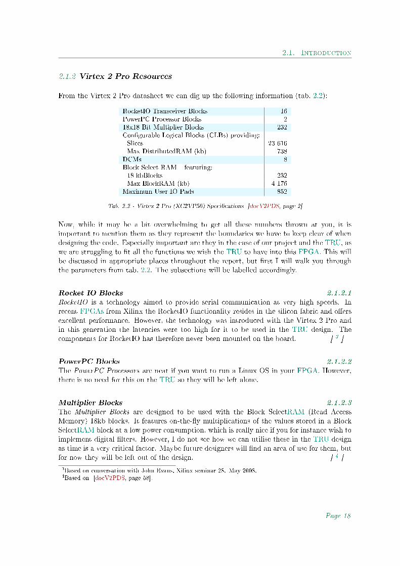
From the Virtex 2 Pro datasheet we can dig up the following information (tab. 2.2):
RocketIO Transceiver Blocks 16PowerPC Processor Blocks 218x18 Bit Multiplier Blocks 232Congurable Logical Blocks (CLBs) providing:Slices 23 616Max DistributedRAM (kb) 738
DCMs 8Block Select RAM+ featuring:18 kbBlocks 232Max BlockRAM (kb) 4 176
Maximum User IO Pads 852
Tab. 2.2 - Virtex 2 Pro (XC2VP50) Specications [docV2PDS, page 2]
Now, while it may be a bit overwhelming to get all these numbers thrown at you, it isimportant to mention them as they represent the boundaries we have to keep clear of whendesigning the code. Especially important are they in the case of our project and the TRU, aswe are struggling to t all the functions we wish the TRU to have into this FPGA. This willbe discussed in appropriate places throughout the report, but rst I will walk you throughthe parameters from tab. 2.2. The subsections will be labelled accordingly.
Rocket IO Blocks 2.1.2.1
RocketIO is a technology aimed to provide serial communication at very high speeds. Inrecent FPGAs from Xilinx the RocketIO functionality resides in the silicon fabric and oersexcellent performance. However, the technology was introduced with the Virtex 2 Pro andin this generation the latencies were too high for it to be used in the TRU design. Thecomponents for RocketIO has therefore never been mounted on the board. [ 3 ]
PowerPC Blocks 2.1.2.2
The PowerPC Processors are neat if you want to run a Linux OS in your FPGA. However,there is no need for this on the TRU so they will be left alone.
Multiplier Blocks 2.1.2.3
The Multiplier Blocks are designed to be used with the Block SelectRAM (Read AccessMemory) 18kb blocks. It features on-the-y multiplications of the values stored in a BlockSelectRAM block at a low power consumption, which is really nice if you for instance wish toimplement digital lters. However, I do not see how we can utilise these in the TRU designas time is a very critical factor. Maybe future designers will nd an area of use for them, butfor now they will be left out of the design. [ 4 ]
3Based on conversation with John Evans, Xilinx seminar 28. May 2008.4Based on [docV2PDS, page 58].
Page 18

2.1. Introduction
Congurable Logic Blocks (CLB) 2.1.2.4
The Congurable Logic Blocks (CLBs) are the main logic resource for implementing sequentialas well as combinatorial circuitry. Since it is an extremely important resource to understandwhen designing the logic for the FPGA, I made a drawing of how these logic blocks are builtup in the Virtex 2 Pro (g. 2.3):
Slice
X1Y1
Switch
Matrix
Shift
Slice
X1Y0
Slice
X1Y0
Slice
X1Y0
Carry Logic
Carry Logic
Carry Logic
Fast
Connects
to
Neigh-
bouring
CLBs
LUTG
or
SRL16
or
RAM16
LUTG
or
SRL16
or
RAM16
Arthmetic Logic
ORCY
MUXFx
Carry Logic
Carry Logic
MUXF5
Register
Or
Latch
Register
Or
Latch
Fig. 2.3 - A Simplied Illustration of the Virtex 2 Congurable Logic Block (CLB)[docV2PDS, page 45] [sofPPT]
First, have a look the right side of g. 2.3 and notice what is called a slice. A slice isthe smallest group of logic in the FPGA, and consists of 2 lookup-tables (LUTs), 2 storageelements, a few multiplexers and a some gates, chains and tri-state buers. A slice is fullycongurable, which means that it can be programmed to realise almost any digital circuitry.
Each lookup table (LUT) has 4 inputs and can be congured either as a function generator,16 bits of read-access memory (Distributed SelectRAM ) or a 16 bits shift register (SRL).When congured as a function generator it can cover all boolean functions of 4 inputs (bysimply looking them up), but with the use of the multiplexers functions for up to 9 inputscan be realised within a single slice. A 2 input multiplexer can be implemented with 1 func-tion generator and some associated multiplexers in the slice, where each additional functiongenerator added will provide 2 extra inputs to the multiplexer.
The Distributed SelectRAM blocks have one address port for synchronous write and - if it iscongured as dual-port - one address port for asynchronous read. The extra port will alwaysrequire the use of an additional LUT, for instance will a 16 bits RAM block with dual portrequire 2 LUTs as opposed to 1 LUT for the single port version.
Page 19
2.1. Introduction
When the LUT is congured as a shift register the write will be synchronous, while the valuesmay be read asynchronously with the 4-bit address bus. If a synchronous read is requiredthe storage element may be utilised. This will also improve the system performance sincethe storage element provides far superior clock-to-out speed.
The storage elements can be congured either to realise a level triggered latch or an edgetriggered register. The input data can either be supplied from logic inside or outside of theslice.
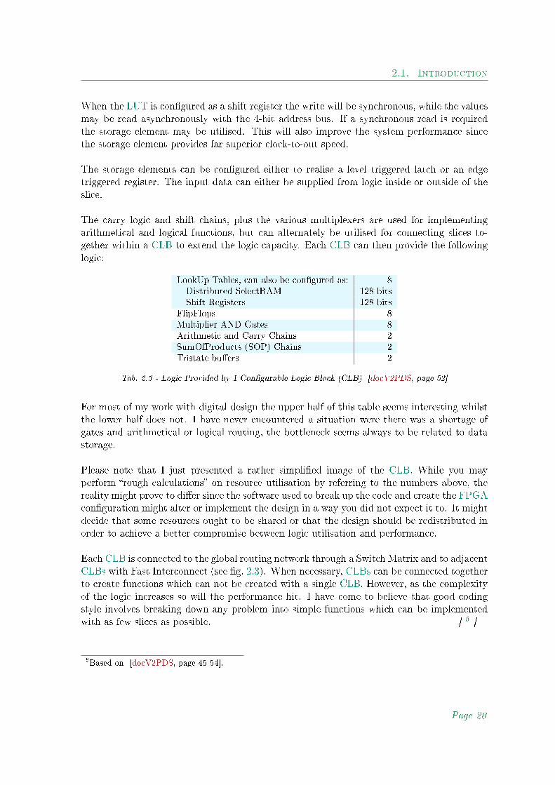
The carry logic and shift chains, plus the various multiplexers are used for implementingarithmetical and logical functions, but can alternately be utilised for connecting slices to-gether within a CLB to extend the logic capacity. Each CLB can then provide the followinglogic:
LookUp Tables, can also be congured as: 8Distributed SelectRAM 128 bitsShift Registers 128 bits
FlipFlops 8Multiplier AND Gates 8Arithmetic and Carry Chains 2SumOfProducts (SOP) Chains 2Tristate buers 2
Tab. 2.3 - Logic Provided by 1 Congurable Logic Block (CLB) [docV2PDS, page 52]
For most of my work with digital design the upper half of this table seems interesting whilstthe lower half does not. I have never encountered a situation were there was a shortage ofgates and arithmetical or logical routing, the bottleneck seems always to be related to datastorage.
Please note that I just presented a rather simplied image of the CLB. While you mayperform rough calculations on resource utilisation by referring to the numbers above, thereality might prove to dier since the software used to break up the code and create the FPGAconguration might alter or implement the design in a way you did not expect it to. It mightdecide that some resources ought to be shared or that the design should be redistributed inorder to achieve a better compromise between logic utilisation and performance.
Each CLB is connected to the global routing network through a Switch Matrix and to adjacentCLBs with Fast Interconnect (see g. 2.3). When necessary, CLBs can be connected togetherto create functions which can not be created with a single CLB. However, as the complexityof the logic increases so will the performance hit. I have come to believe that good codingstyle involves breaking down any problem into simple functions which can be implementedwith as few slices as possible. [ 5 ]
5Based on [docV2PDS, page 45-54].
Page 20

2.1. Introduction
Digital Clock Managers 2.1.2.5
The Virtex 2 Pro FPGA has a wide variety of interconnect for routing data and clocksignals6.For global clock signals, or for very high speed clocks the global clock routing network shouldbe used. This is because it is the only net which is directly connected to everything in theFPGA, thus providing shared timing models). This network can host a maximum of 16clocks, but with restrictions. To clarify, I made an illustration (g. 2.4):
Input and outputs (I/O pads and pins)
8 IBUFG
S0
0S1P2S3P4S5P6S7P
0P1S2P3S4P5S6P7S
8 BUFGMUX
DCM DCM
BRAM BRAM
DCM DCM
BRAM BRAM
DCM DCM
BRAM BRAM
DCM DCM
BRAM BRAM
NW
SW
NE
SEBANK 7
BANK 6
BANK 5
BANK 4
BANK 3
BANK 2
BANK 1
BANK 0
CLB CLB
8 IBUFG
8 BUFGMUX
8 BUFGMUX8 BUFGMUX
8 IBUFG8 IBUFG
The Code
The Code
Fig. 2.4 - Virtex 2 Pro Global Clock Distribution [docV2PUG, page 69] [sofPPT]
The global clock network is made up of 8 banks or clockmultiplexer pairs, each of whichcontains a primary and secondary clockmultiplexer (or buer, e.g. BUFGMUX 0S and 0P)7.Each multiplexer pair shares routing resources in the same quadrant of the FPGA (NW,SW, NE, SE, according to geometrical direction), so if the primary buer access the NWquadrant, the secondary buer may only access the remaining 3 quadrants. The input tothe global clock buers can come from either the global input clock pins (IBUFG)8, frominternal logic or from Digital Clock Managers (DCMs, described on the next page).
6For a nice hierarchical overview of the Virtex 2 Pro interconnect, refer to [docV2PDS, page 65].7Global clock MUXs can shift glitch-lessly from one clock to another.8Global clock pins can drive DCMs on the same clock edge.
Page 21

2.1. Introduction
While the global clock network is the best suited for distributing clocks in the design, sec-ondary clocks or high fan-out signals can be routed using a pattern of alternative routingresources (long lines9, hex lines, double lines, ..)10 that results in low skew, but the bestresults are usually achieved by letting the implementation software handle it single-handedly.When you need to specify some timing criterias use timing constraints.
A Digital Clock Manager (DCM) is a self-calibrating and fully digital solution for:
• Clock distribution. Source a clock signal to it and let it supply internal logic or externalcomponents with high quality clock signals. The fan-out capability is very good andthe phase-locked loop (PLL) inside the DCM will assure perfect duty-cycle.
• Delay compensation. Use the post-buer clock signal as feedback to make the DCMtransparent (clock has same phase before and after DCM).
• Clock frequency multiplication and division. Create derived clocks with a wide range ofpossible frequencies.
• Coarse-grained clock phase shifting. Supplies output clocks with 0, 90, 180 and 270
phaseshifts, respectively.
• Fine-grained clock phase shifting. Provides the ability to on-the-y adjust the clockphase in increments of T/25611. [ 12 ]
Block Select RAM 2.1.2.6
The BRAM blocks you see in g. 2.4 are the 18kb Block SelectRAM mentioned in tab. 2.2. Itfeatures two synchronous ports where the width is programmable from 1 bit (depth 16 384bits) to 36 bit wide (depth 512 bits). Each port has an address bus which is independentlyclocked. It is not as fast as the shallow CLB memory, but will in return provide massivestorage space. [ 13 ]
Input and Output Buers 2.1.2.7
The Input and Output Buers (IOB) is the interface between the external (outside FPGA)and internal logic. For both inputs and outputs a wide range of signalling standards aresupported - for both dierential and single ended schemes. Optional input delay elementsmay be used to synchronise input data streams, and input impedance can be selected eitherdigitally (with Digitally Controlled Impedance, DCI) or by toggling an input terminationparameter. Each IOB buer has several registers, for driving the output pins or for clockinginput data (even Dual Data Rate - DDR (Dual Data Rate)- is supported). However, thedata may also just be routed through.
9The long lines are often referred to as the backbone, you can force your design to use them with theUSELOWSKEWNETS constraint.
10All interconnect is designed to minimise crosstalk, so for internal logic this does not need to be evaluated.11Overridden by DCM_TAP_MIN and DCM_TAP_MAX, the minimum increment seems to be ≈40ps.12Based on [docV2PDS, page 61-65] [docV2PUG, page 68-84, 89-93].13Based on [docV2PDS, page 54-57].
Page 22

2.1. Introduction
2.1.3 History
From the previous subsection you have learned what resources the TRU FPGA has to oer.I will shortly take this one step further as I present my work the digital design (see 2.2).However, as many people has been working with the TRU prior to my arrival, I nd itappropriate to provide an abstract of the work done so far (tab. 2.4):
Date: Event:
2004 First TRU (v1.0) card proposed by Hans Muller.Two versions: PHOS: v1.0a, EMCAL (ElectroMagnetic CALorimeter): v1.0e.
2004/2005 Board design (schematics, layout, ..) completed by Rui Pimenta.2005 Alexandra Oltean starts with code design. Major work put into a deserialiser
using oversampling.2006 A PCB layout with Cadence Allegro is made by Xi Cao.2006 The PCB layout is produced with two prototypes in Wuhan, China.2006 The prototypes are tested. Linfeng He (China) is improving the digital design
(reset schemes, verications, BoardController).2006/2007 Rui Cai (China) started to work on hardware verications (signal termination
at the ADCs, ADC bias schemes, FEE channel mapping).2007 Nicolas Degrenne (France) continues Rui Cais work.2007 Alan Crouau (France) picks up the lead after Nicolas, and performs major work
related to improvement of the deserialiser and creates the rst prototype codefor TRU-TOR data transmission.
2007 I arrive and spend a few months with Alan where he unloads some of his acquiredknowledge to me, and where we discuss ideas for future TRU development.
2007 A revision of the TRU hardware design is done by Rui Pimenta and Xi Cao.2007 New TRUs (v1.1) are produced and tested in Wuhan, China.2008 The rst PHOS module is installed in ALICE and with it 8 TRUs (v1.0a).2008 Dong Wang (China) will resume TRU development where I left it.
Tab. 2.4 - TRU History [docNICOLAS, top part from page 88]
Let us move on to the digital design, shall we?
Page 23
2.2. Digital Design
2.2 Digital Design
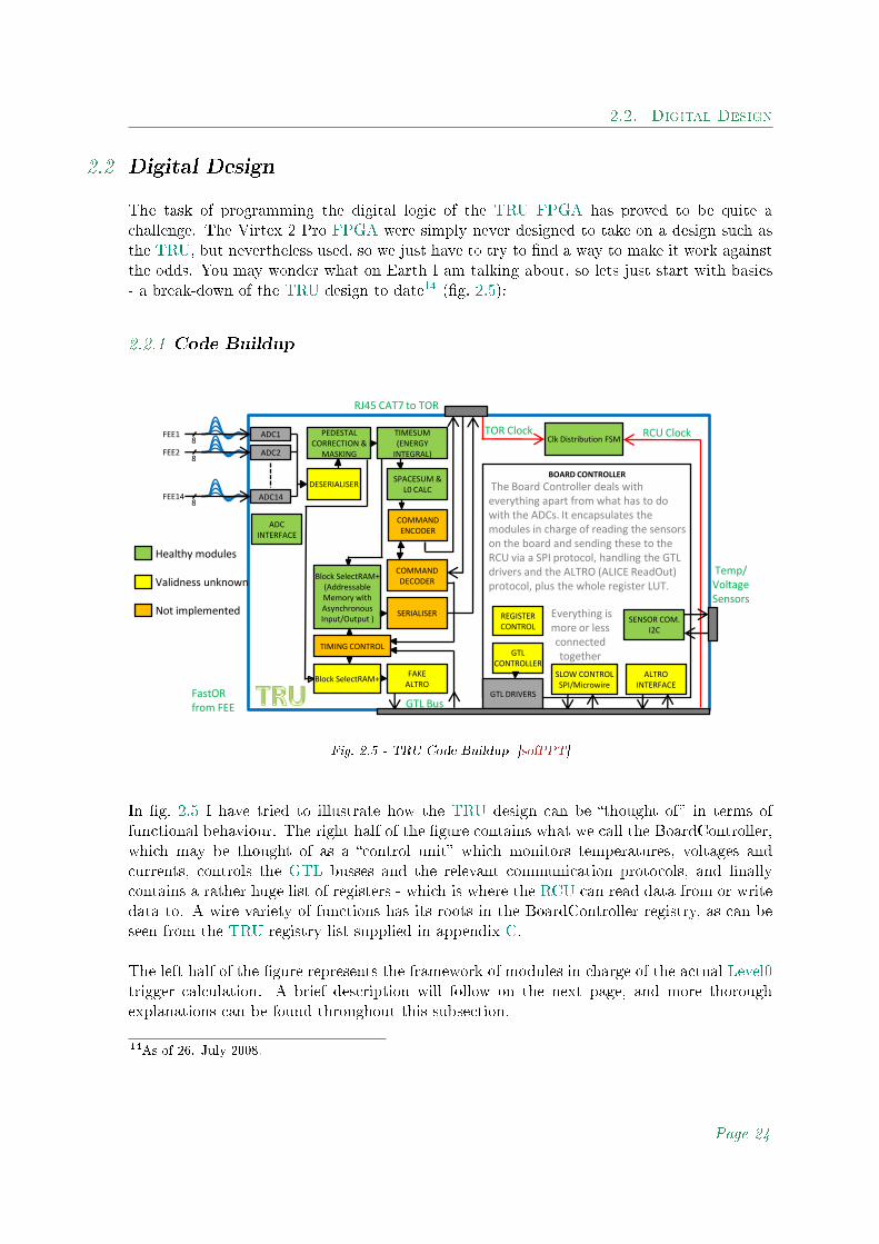
The task of programming the digital logic of the TRU FPGA has proved to be quite achallenge. The Virtex 2 Pro FPGA were simply never designed to take on a design such asthe TRU, but nevertheless used, so we just have to try to nd a way to make it work againstthe odds. You may wonder what on Earth I am talking about, so lets just start with basics- a break-down of the TRU design to date14 (g. 2.5):
2.2.1 Code Buildup
FastOR from FEE
8FEE1
8FEE2
8FEE14
ADC1
ADC2
ADC14
DESERIALISER
PEDESTAL CORRECTION &
MASKING
SPACESUM &L0 CALC
COMMAND ENCODER
Block SelectRAM+(Addressable Memory withAsynchronous Input/Output )
COMMAND DECODER
FAKEALTRO
GTL Bus
SERIALISER
TIMESUM(ENERGY
INTEGRAL)
Block SelectRAM+
TIMING CONTROL
BOARD CONTROLLER
GTL DRIVERS
SLOW CONTROLSPI/Microwire
SENSOR COM.I2C
ALTRO INTERFACE
GTL CONTROLLER
RJ45 CAT7 to TOR
Temp/Voltage Sensors
REGISTERCONTROL
ADC INTERFACE
Clk Distribution FSMRCU ClockTOR Clock
Everything is more or less connected together
The Board Controller deals with everything apart from what has to do with the ADCs. It encapsulates the modules in charge of reading the sensors on the board and sending these to the RCU via a SPI protocol, handling the GTL drivers and the ALTRO (ALICE ReadOut) protocol, plus the whole register LUT.
Healthy modules
Validness unknown
Not implemented
Fig. 2.5 - TRU Code Buildup [sofPPT]
In g. 2.5 I have tried to illustrate how the TRU design can be thought of in terms offunctional behaviour. The right half of the gure contains what we call the BoardController,which may be thought of as a control unit which monitors temperatures, voltages andcurrents, controls the GTL busses and the relevant communication protocols, and nallycontains a rather huge list of registers - which is where the RCU can read data from or writedata to. A wire variety of functions has its roots in the BoardController registry, as can beseen from the TRU registry list supplied in appendix C.
The left half of the gure represents the framework of modules in charge of the actual Level0trigger calculation. A brief description will follow on the next page, and more thoroughexplanations can be found throughout this subsection.
14As of 26. July 2008.
Page 24

2.2. Digital Design
In the upper left corner you can spot the ADCs, coloured grey since they represent hardwareand not programmable logic. There are 14 ADCs in total, each connected to a respectiveFEE card from which it receives 8 FastOR signals. The dynamic range of the ADC inputsis ±1V (linear range, input bias within a few mV), which is digitised with 12 bits accuracy(resulting in a resolution of 2V/212 ≈ 0.5mV) at 40MHz. These bits are then sent serially tothe FPGA at both edges of a 240MHz clock, eectively creating a bitrate of 480Mbps.
When these bits arrive at the FPGA they rst need to be synchronised with the internalclock of the FPGA (see 2.2.5), and then deserialised (see 2.2.6). Several factors related tothe operation of the ADCs may be controlled with a dedicated ADC interface (see 2.2.4).
Each FastOR pulse is around 100ns long, which can be represented with 4 samples in our40MHz digital world. As only the positive part of the FastOR pulses contains any valuableinformation, the average is subtracted on a per-channel basis (referred to as pedestal sub-traction, see 2.2.7). If the channels are noisy they may be masked out with the use of amask register. We call the data at this point raw data. Since this is the type of data theFakeALTRO protocol are meant to ship to the RCU upon request, it will be stored in a BlockSelectRAM element which can retain a history of 256 samples (equals 6.4µs).
The Level0 trigger is based on an evaluation of the energy in a shower of photons. In timethe energy is spread out over 100ns (the length of the FastOR pulse). To integrate the energyin time, we simply sum up the 4 samples which describes the respective FastOR pulse. Atthis point we call the data time summed (see 2.2.7), which is the type of data the TOR needsin order to calculate the Level1 trigger. Similar to the raw data storage for the FakeALTROprotocol, the time summed data will be sent in a Block SelectRAM element retaining ahistory of 256 samples.
When particles hit the PHOS crystals the light might disperse into several adjacent crystals15.In order to get a scalar representing the total energy of the particle, we will need to sum upmatrices of 4x4 crystals (referred to as space summing, see 2.2.7). As each of the FastORsignals represent the sum of 2x2 crystals, the 4x4 sum can be calculated by summing 2x2FastOR signals. All possible combinations of 2x2 FastOR signals will be summed (the ideabeing that at least one of these squares be be centered over the particle entry point), butas the edges of the branch can not be summed (the TRU can not see across the branchboundaries) only 91 space sums may be calculated out of the 112 FastOR signals received16.
If the energy of any of the 91 space+time summed values exceeds a certain set threshold, aLevel0 trigger will be generated. It is currently sent to the TOR on a dedicated line, but thismight change as the TOR communication interface is being developed (see 2.2.8).
15The dispersion factor is both a function of the particle angle and size.16From the 112 FastOR signals (14 FEEs (z-axis) times 8 channels (x-axis)) only 13x7=91 squares of 2x2
FastOR signals may be summed. Only the Level0 calculation will suer from this aw; only time summeddata will be sent to the TOR which allows it to re-do the space sum without the branch boundary limitation(the TOR receives data from all TRUs, thus the only boundary will be those of the PHOS module).
Page 25

2.2. Digital Design
2.2.2 General Design Changes
I have made quite a few general edits to the code since the version of the TRU code I receivedupon arrival (see [srcTRUDESIGN]). They are summarised in the following list:
• Conversion to Verilog 2001. The design code I received used almost extensively theVerilog 95 syntax, which means no multidimensional arrays, no generate statements,and port lists where the ports had to be redened 3 times in order to declare the name,direction and type, respectively. For those of you who are not into the terminology:The design code very quickly becomes very messy and very huge. I suggest that youload a few source les from the new code and the old to see the dierence.
• Rewriting functions to improve logic distribution. The old design used synchronousdesign elements for everything17. Even for concurrent arithmetical operations whereonly the end results were interesting, the data was clocked into respective registersalong the way. The main advantage of such an approach is that design elements canrun at very high speeds, but as the TRU base clock runs at 40MHz (which is considereda low/moderate speed) this involves bad performance (as for the greatest part of a clockcycle nothing will get done) and a non-optimal logic distribution (as in my experiencethe design works best with a balanced logic usage). As registers were always thebottleneck in the old design, and the alternative resources were hardly used, the logicshould be redistributed.
• Design altered to better integrate with future design elements. High up on the wish-listfor my supervisor at CERN and other people in my project were the communicationinterface to the TOR and the FakeALTRO interface for the RCU. The former is nec-essary if we want the Level1 trigger in PHOS as the TOR can not calculate anythingwithout any raw data from the Level0 trigger event. The FakeALTRO, is, as the nameimplies, a fake ALICE ReadOut protocol. It enables the RCU to read out the rawdata from the TRU in the same way as it reads out the raw data from the FEE cards(from the ALTRO (ALICE ReadOut) chips [docALTRORC]). Both design objects re-quires access to the relevant data, but as storage is limited I redesigned the code a bitin order for it to be plug-and-play with these functions - with a minimum of extra logicrequired.
The rest of this subsection will deal with design elements which I altered or added. In thenext subsection I will talk about which clock domains the TRU must relate to (see 2.2.3).
17If you think like in a high-level programming language when designing hardware, you will end up withthe register elements (in a CLB, see 2.1.2.4) as your bottleneck. The reason is simple: What is storedin the registers are always accessible at any given time (not like in a RAM where only some addressedbits can be accessed at a given time), which provides data in exactly the same state as in a high levelvariable.
Page 26
2.2. Digital Design
2.2.3 Managing Clocks
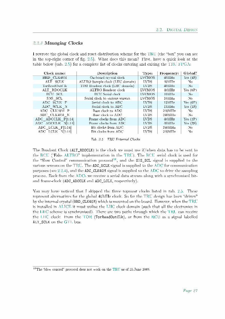
I rewrote the global clock and reset distribution scheme for the TRU (the box you can seein the top-right corner of g. 2.5). What does this mean? First, have a quick look at thetable below (tab. 2.5) for a complete list of clocks entering and exiting the TRU FPGA:
Clock name: Description Type: Frequency: Global?
BRD_CLK40M On-board crystal clock LVCMOS 40MHz Yes (4S)ALT_SCLK ALTRO Sample clock (LHC domain) LVDS 40MHz No
TorReadOutClk TOR Readout clock (LHC domain) LVDS 40MHz NoALT_RDOCLK ALTRO Readout clock LVCMOS 40MHz Yes (6P)
RCU_SCL RCU Serial clock LVCMOS 10MHz NoSNS_SCL Serial clock to various sensors LVCMOS 10MHz No
ADC_SCLK_P Serial clock to ADC LVDS 13MHz Yes (0P)ADC_SCLK_N Serial clock to ADC LVDS 13MHz Yes (1S)
ADC_CLK40M_P Base clock to ADC LVDS 240MHz NoADC_CLK40M_N Base clock to ADC LVDS 240MHz No
ADC_ADCCLK_P[1:14] Frame clocks from ADC LVDS 40MHz Yes (2P)ADC_ADCCLK_N[1:14] Frame clocks from ADC LVDS 40MHz Yes (3S)ADC_LCLK_P[1:14] Bit clocks from ADC LVDS 240MHz NoADC_LCLK_N[1:14] Bit clocks from ADC LVDS 240MHz No
Tab. 2.5 - TRU External Clocks
The Readout Clock (ALT_RDOCLK) is the clock we must use if/when data has to be sent tothe RCU (Fake ALTRO implementation in the TRU). The RCU serial clock is used forthe Slow Control communication protocol18, and the SNS_SCL signal is supplied to thevarious sensors on the TRU. The ADC_SCLK signal is supplied to the ADC for communicationpurposes (see 2.2.4), and the ADC_CLK40M signal is supplied to the ADC to drive the samplingprocess. Back from the ADCs we receive a serial data stream along with a synchronised bit-and frame-clock (ADC_ADCCLK and ADC_LCLK, respectively).
You may have noticed that I skipped the three topmost clocks listed in tab. 2.5. Theserepresent alternatives for the global 40MHz clock. So far the TRU design has been drivenby the internal crystal (BRD_CLK40M) which is mounted on the board. However, when the TRUis installed in ALICE it must utilise the LHC clock domain (such that all the electronics inthe LHC scheme is synchronised). There are two paths through which the TRU can receivethe LHC clock: From the TOR (TorReadOutClk), or from the RCU as a signal labelledALT_SCLK on the GTL bus.
18The slow control protocol does not work on the TRU as of 25.June 2008.
Page 27

2.2. Digital Design
What we want to do here is to have both the LHC clock and the crystal clock connectedto their respective DCM, and connect the output clocks to a global clock multiplexer19.The multiplexer should be controlled with the LOCKED signal of the LHC clock DCM (whichindicates whether the LHC clock is present) such that the LHC clock is used wheneverpossible.
I mentioned that I ended up redesigning the entire clock and reset distribution scheme. Thiswas caused by the following factors:
• The need to create the global clock multiplexer (as previously mentioned) interferedwith the old global reset scheme.
• The old ADC control modules were nested into the clock and reset scheme. Thiswas confusing, and since I needed a control mechanism with more features anyway Iredesigned both this and the clock distribution module.
• The old clock distribution code was messy. It was modied many times by severalpeople and proved to be very hard to read. Some design choices were also bad, forinstance was the clock supplied to the ADCs gated through ip-ops. This is not anoptimal solution since these logical blocks were never designed to provide high qualityclock signals. A high quality clock has perfect phase and duty cycle, rapid rise/fall timesand are guaranteed to be glitch free. With bad clocks we may quickly nd ourselvesstruggling with metastability issues [intMETA].
• There were quite a few remains from previous deprecated design elements. Cleaningup the code is important in order to get a clear picture of what you are doing.
The clock distribution design elements are encapsulated in the InitAndClkDist module inthe TRU design code [srcTRUDESIGN], have a look if you are interested. In the nextsubsection we will take a look at the ADC interface, which - among other features - containsthe control modules that were removed from the global clock scheme.
19Note that the clock multiplexing scheme is not present in my last version of the code as I never got aroundto re-add it after I reverted my code to an older version in my work with the ADC synchronisation, see2.2.5.
Page 28

2.2. Digital Design
2.2.4 ADC Communication
The TRU-ADC interaction is split into two parts: (1) Communication between the tworequired in order to alter the default behaviour of the ADCs, and (2) dealing with thesampling process. Take a look at g. 2.6 to see how it all ts together. This subsection willdeal with the communication protocol, while the next (see 2.2.5) will describe the variouschallenges related to ADC data synchronisation.
ADC_SCLK
MPC9109
ADC_CLK40M_P
ADC_CLK40M_N
@40MHz
ADC_RESET
ADC_CS
ADC_SDATA
ADC_ADCCLK_P
ADC_ADCCLK_N
ADC_LCLK_P
ADC_LCLK_N
InitAdc
AdcClkDCM
DCM
@13.3MHz
AdcData
Pusher
Adc
Control
reg0x72
RESET
SDATA
CS1
1
141
13
13
1
14
1
1
1
Settings
Sampling
TriggerOut
Input
from
FEE
cards
FastOR
8
@40MHz
@240MHz
ADC_QUAD_P
ADC_QUAD_N@480Mbps
13
13
13
13
104
104 8
8
1
1
1
114
14
14
14
112
112
Deserialiser
Pedestal Correction
Time Integral
Space Integral
L0 Calculation
ReadOut
Clock
For Clock
Distribution
Fig. 2.6 - ADC Interaction [sofPPT]
Motivation 2.2.4.1
The TRU had an ADC interface module which were located in the BoardController. WhenI was redesigning the deserialiser (see 2.2.6) the need to know exactly what input to expectfrom the ADCs arose. Since the ADCs are capable of sending out custom patterns, I re-searched how to set them up in such a way. Basically, you will need to send a few 8 bit wordsto the ADCs via a SPI/Microwire serial protocol. However, even though there was already aTRU module aimed to provide this functionality, I was not able to get the the ADC interfaceworking (it was not even connected initially) and could not nd any documentation on itsinner workings.
So I went ahead and made my own protocol, and here is the documentation!
Page 29

2.2. Digital Design
Communication Protocol 2.2.4.2
In the lower half of g. 2.6 you will nd the relevant signals and blocks that make up thecommunication system. Basically, the communication is a one way deal where the TRU tellsthe ADCs how to behave. It does so by targetting the relevant ADCs through the use of theChipSelect lines (ADC_CS[13:0]), one for each ADC. An ADC accepts the communicationwords when the ChipSelect line is low. The command word is sent serially over the dataline (ADC_SDATA) with MSB (Most Signicant Bit) rst, which is and clocked into theADC on positive edge of the dedicated clock line (ADC_SCLK ). This clock has the samesource as the 40MHz clock driving the sampling process, but is 3 times slower.
The module AdcControl listens to reg0x7c (bits [7:0]) and will initiate a process of updatingall the ADCs with the relevant data should the change prove to be stable for at least 5 clockcycles. The data in reg0x7c[7:0] corresponds to the bits D7:D0 of the command wordyou wish to send to the ADCs (for all possible commandwords see C.1). The ADCs arerst targeted by the AdcControl module, then the control is handed to the AdcDataPushermodule which will send the word according to protocol.
As a precaution measure I set the AdcControl module up to update only one ADC at a time.A chronogram of the whole process undergoing simulation can be found in g. B.1.
Conclusion 2.2.4.3
The communication with the ADCs seems to be working awlessly. I have used it extensivelyto adjust the output current of data and clock signals, set up various data patterns (forsynchronisation or deskew purposes) and to power up/down channels while debugging thedesign. For a complete list of possible commands, have a look at register 0x7c in the TRUregister list (see C.3).
While the communication interface works nicely now, it would also be nice to specify settingsfor only a certain set of ADCs. As the protocol is currently designed, the 8 least signicantbits of the value held by register 0x7c is written to every ADC. Maybe the remaining 8 mostsignicant bits of this register could be used to specify which ADCs should be updated withthe value set? I never got around to do this myself.
The module containing these relevant design elements is labelled InitAdc, look it up in theTRU design (see [srcTRUDESIGN]). Now, let us take a look at the data synchronisationpart of the ADC interface.
Page 30

2.2. Digital Design
2.2.5 ADC Data Synchronisation
As you can see from g. 2.6, the ADCs receives - in addition to the communication clock(ADC_SCLK ) - a clock operating at 40MHz (ADC_CLK40M ) which is fed into the ADCPLL (Phase Locked Loop) to drive the sampling process. The PLL - used to assure perfectduty cycle and low skew internal clock distribution - can not operate at frequencies lowerthan 20MHz or higher than 40MHz. These are the boundaries within which we have to keepour sampling speed in order to get predictable results.
The FastOR signals are digitised into 12 bit samples at a 40MHz frequency. Each ADC inputhas a dynamic range of ±1 V, which translates to an eective sample resolution of ≈500µV.The bits are sent serially to the FPGA 20 over the dedicated data lines21 (ADC_QUAD), withan accompanying bit-clock (ADC_LCLK ) and word-clock (ADC_ADCCLK ) that can beused to ease the deserialisation process. The serial approach means less interconnect (henceless EMI (ElectroMagnetic Interference) and possibly higher speed), less clock-to-data skew,and allows the designer to choose an FPGA with fewer pins (which will reduce the cost a lotin big designs). The drawback is that a deserialiser must be implemented in the other end,which must be done manually in the FPGA used in the PHOS TRU 22.
In this subsection I will deal with the ADC data synchronisation issue, but this topic is alsovery closely related to the ADC data deserialiser, a variant of which will be described in thenext subsection (see 2.2.6).
Motivation 2.2.5.1
To synchronise the ADC data with the internal FPGA clocks has proved to be a big designchallenge for the TRU. Quite a few people has been working on this issue, with varying degreeof success. When I received the TRU code from Alan Crouau he was very close to a fullyworking solution. On the next page I supply an illustration (g. 2.7) of a readout I performedof the entire PHOS module 2 while it was installed in ALICE 23, which used Alans design.I manually read the TRU ADCs out with ChipScope (see A.2.3), then roughly calculatedthe size of the average noise in ADC counts. These values I then put in the coordinationsystem (of the ADC channels) you can see in g. 2.7. Green and blue channels are more orless healthy, but the red and yellow ones are not. This is a synchronisation problem.
20The user can dene whether MSB or LSB (Least Signicant Bit) are to be sent rst with the use of theADC communication interface (see 2.2.4.2)
21The datalines are designed such that they all have the same length. This is in order to match up the phaseof the data as good as possible at the FPGA entry point.
22The Xilinx Virtex-II Pro FPGA which does not support hardware deserialisation.23Readout performed 11. July 2008.
Page 31
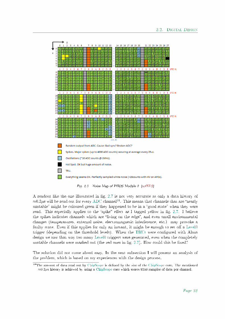
2.2. Digital Design
Fig. 2.7 - Noise Map of PHOS Module 2 [sofXLS]
A readout like the one illustrated in g. 2.7 is not very accurate as only a data history of≈0.2µs will be read out for every ADC channel24. This means that channels that are nearlyunstable might be coloured green if they happened to be in a good state when they wereread. This especially applies to the spike eect as I tagged yellow in g. 2.7. I believethe spikes indicates channels which are living on the edge, and even small environmentalchanges (temperatures, external noise, electromagnetic interference, etc.) may provoke afaulty state. Even if this applies for only an instant, it might be enough to set o a Level0trigger (depending on the threshold levels). When the TRUs were congured with Alansdesign we saw that way too many Level0 triggers were generated, even when the completelyunstable channels were masked out (the red ones in g. 2.7). How could this be xed?
The solution did not come about easy. In the next subsection I will present an analysis ofthe problem, which is based on my experiences with the design process.
24The amount of data read out by ChipScope is dened by the size of the ChipScope core. The mentioned≈0.2µs history is achieved by using a ChipScope core which stores 8188 samples of data per channel.
Page 32

2.2. Digital Design
Problem Breakdown 2.2.5.2
TriggerOut
ADC_QUAD_P*8
8
ADC_QUAD_N*
8
Bit rate
~2ns
”Golden Eye”
~1ns
ADC_QUAD_P*8
8
ADC_QUAD_N*
8
ADC_QUAD_P*8
8
ADC_QUAD_N*
8
ADC_QUAD_P*88
88
ADC_QUAD_N*
88
A ”common” eye for all
channels hardly exist.
The data from the ADCs
are not in phase when
arriving at the FPGA.
Time where the data is
valid for all channels
AdcDeserialiser
Z=50?
Input impedance
must be perfect!
8
D DDD
4
DDD D
4
Due to the propagation time
of the signals in the FPGA
interconnect the data will
arrive slightly delayed at
the synchronous storage
element. The important
factor here is not the
delay itself but the skew
(delay difference). The skew
is also affecting the clock,
so tight constraining and
manual place&route will
probably be needed.
Fig. 2.8 - Synchronising the ADC Databits [sofPPT]
Fig. 2.8 shows the key aspects of concern when the ADC data is to be synchronised. Thekey factor here is the high 480Mbps data bit rate, eectively causing problems with:
• Signal integrity. As the speed of clock and data signals increases the signal qualitygenerally tend to decrease. Even small impedance mismatches may cause big signalreections, and parasitic components such as capacitive load will kill the signal edges.The duty cycle of clock signals may deteriorate as a function of jitter (unintended phasevariations) and the golden eye of the data will shrink25.
• The datasignals arrive at the FPGA with dierent phases. One ADC has 8 channels,each of which is providing datasignals with relatively low skew (≈100ps). However, thethe skew is much higher if channels from several ADCs are considered. This meansthat the common golden eye is very small, or hardly exists at all.
• Delays in the FPGA routing network. When signals are to be distributed internally inthe FPGA, delays of a few ns from source to destination are not uncommon (dependingon the type of interconnect utilised, see 2.1.2.5). Here arises the problem of how tocorrectly synchronise all the bits when the bitrate is higher than the skew of our internalclocks.
• Design verication. The ChipScope module becomes very hard to work with at speedsgreater than 80MHz, which means that you must validate this part of the design insimulation and hope for the best when conguring the FPGA with it (which works wellfor low speed designs, but not at all for high speed designs).
25The golden window is the timeinterval of which the data is stable.
Page 33
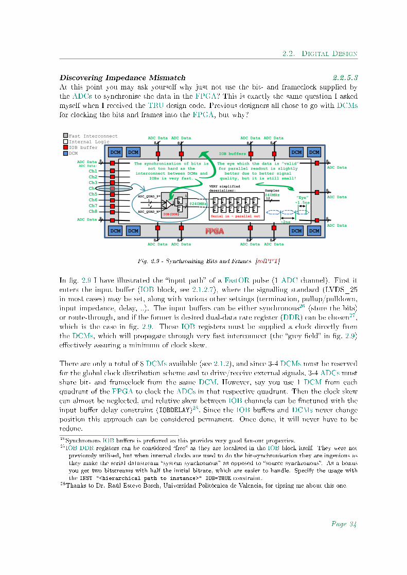
2.2. Digital Design
Discovering Impedance Mismatch 2.2.5.3
At this point you may ask yourself why just not use the bit- and frameclock supplied bythe ADCs to synchronise the data in the FPGA? This is exactly the same question I askedmyself when I received the TRU design code. Previous designers all chose to go with DCMsfor clocking the bits and frames into the FPGA, but why?
DCM DCM
DCM DCM
DCM DCM
DCM DCM
8
8
ADC Data:
Ch1
Ch2
Ch3
Ch4
Ch5
Ch6
Ch7
Ch8
8 8 8 8
8 8 8 8
ADC Data ADC Data ADC Data ADC Data
ADC Data
ADC Data
ADC Data
ADC DataADC DataADC DataADC Data
8
8
8
ADC Data
ADC Data
The synchronisation of bits is
not too hard as the
interconnect between DCMs and
IOBs is very fast.
IOB buffers
1
1
ADC_QUAD_P*
ADC_QUAD_N*IOB(DDR)
D
D1
1
1
Serial in - parallel out
DDDDDD
DDDDDD
12
The eye which the data is ”valid”
for parallel readout is slightly
better due to better signal
quality, but it is still small!
VERY simplified
deserialiser: Samples
”Eye”
~1.5ns
~2ns
@40MHz
@240MHz
Fast Interconnect
Internal Logic
IOB buffer
DCM
Fig. 2.9 - Synchronising Bits and Frames [sofPPT]
In g. 2.9 I have illustrated the input path of a FastOR pulse (1 ADC channel). First itenters the input buer (IOB block, see 2.1.2.7), where the signalling standard (LVDS_25in most cases) may be set, along with various other settings (termination, pullup/pulldown,input impedance, delay, ..). The input buers can be either synchronous26 (store the bits)or route-through, and if the former is desired dual-data rate register (DDR) can be chosen27,which is the case in g. 2.9. These IOB registers must be supplied a clock directly fromthe DCMs, which will propagate through very fast interconnect (the grey eld in g. 2.9)eectively assuring a minimum of clock skew.
There are only a total of 8 DCMs available (see 2.1.2), and since 3-4 DCMs must be reservedfor the global clock distribution scheme and to drive/receive external signals, 3-4 ADCs mustshare bit- and frameclock from the same DCM. However, say you use 1 DCM from eachquadrant of the FPGA to clock the ADCs in that respective quadrant. Then the clock skewcan almost be neglected, and relative skew between IOB channels can be netuned with theinput buer delay constraint (IOBDELAY)28. Since the IOB buers and DCMs never changeposition this approach can be considered permanent. Once done, it will never have to beredone.26Synchronous IOB buers is preferred as this provides very good fan-out properties.27IOB DDR registers can be considered free as they are localised in the IOB block itself. They were not
previously utilised, but when internal clocks are used to do the bit-synchronisation they are ingenious asthey make the serial datastream system synchronous as opposed to source synchronous. As a bonusyou get two bitstreams with half the initial bitrate, which are easier to handle. Specify the usage withthe INST "<hierarchical path to instance>" IOB=TRUE constraint.
28Thanks to Dr. Raúl Esteve Bosch, Universidad Politécnica de Valencia, for tipsing me about this one.
Page 34

2.2. Digital Design
In g. 2.9 I made an simplied illustration of the simplest deserialiser one can make; clockthe bits into a shift-register consisting of ipops, and clock the data out when all the bitsare in the right position. Naturally, the data is only in the right position for only about2ns (less when jitter is evaluated). This means that such an approach requires a frameclockwith minimal skew (remember, we have to use the same few DCMs to supply frameclocks).But, even if the global clock banks (see 2.1.2.5) are utilised, the skew in the internal logicof the FPGA will be higher than that of the fast interconnect surrounding the IOB buers.How can be synchronise the frameclock in this environment?
My rst take on the situation was to construct a deserialiser which uses Distributed Se-lectRAM (see next section, 2.2.6) to allow the bit- and frameclock to be completely phaseindependent. Basically this means that the frame synchronisation would be directly resolvedin the deserialiser. However, due to problems with verication of the design and shortage oftime I chose to make a deserialiser so simple (like the one shown in g. 2.9) that nothingcould possibly go wrong. I knew it would be hard to get it working on all ADC channels,but for most of them it would (as this was also Alans approach). Then I set one DCM up toprovide the bitclock, and another to provide the frameclock. After creating a few statema-chines I was able to adjust the frameclock with register 0x79, and the bitclock with 0x7a (seeC.3 for a description of the registers, and A.6 for directions on how to use them).
Using the ADC setup register 0x7c, the phase adjust registers 0x79 and 0x7a and ChipScopeto read samples on-the-y I was now able to map the real cause of the deserialiser failure.From ddling with this setup for a while I gained some unexpected but valuable knowledge:
• The phaseinterval where the bit-clock correctly clocked the bits for a couple of ADCs wereat least 400ps (10 values dierence in register 0x7c). This seems to verify my previousstatements; the DCM-IOB interconnect is fast enough for the bits to be clocked witha single clock.
• A bitsequence like 0000 0011 1111 was often interpreted as 0000 0010 1111, and
• data was not stable as a function of ADC output current (drive strength). These twoobservations had me puzzled. Were the ADCs generating patterns which were not inaccordance with the settings I specied? Was the deserialiser still unstable, or werethe ADCs suering from a bad power supply (the given bitpattern causes all 112 ADCchannels to go from 0 to 1 at the same time, which may cause the energy deposits inthe powersupplies to deplete)? Or could there be an impedance mismatch somewhere?
All the TRU input buers were previously congured for the 2.5V LVDS signalling standard,with a dierential termination of 100Ω. Maybe this was not the optimal solution? I trieda few alternatives, and nally found that using buers with Digitally Controlled Impedance(DCI) completely resolved the problem29! With a digitally dened input impedance of 50Ωthe bits were suddenly clocked in perfectly, and the golden window of the datastreamwidened quite a bit!
29The name of the DCI buer I used: LVDSEXT_25_DCI, where EXT means extended and refers to thevoltage range (maximum and minimum ratings).
Page 35

2.2. Digital Design
Conclusion 2.2.5.4
While this subsection could have been merged into the next one dealing with the deserialiser(see 2.2.6), I chose to separate the two in order to specify which elements our synchronisationproblem really consist of. While I have tried to present this information in a way that isnatural to read, the problem was only slowly dened as I started to investigate the reason(s)for why the deserialiser was unable to deliver the correct samples.
To sum it all up, the data may appear badly synchronised if:
• The input buers are slightly miscongured.• The databits are clocked into the input registers when the data is in a metastable state(bad phase of the bitclock).
• The parallel read of bits from a deserialising array of ipops are not synchronisedcorrectly (bad phase of the frameclock).
The rst point were discovered by creating a deserialiser with variable bit- and frameclocks,such that those two factors could be tuned out of the picture. When a better input buer typewas selected, the the results acquired when testing designs with various bit- and frameclockschemes suddenly seemed much more reliable. A disturbing factor had been removed fromthe design.
I also learned that the problem was not as much to synchronise the bitstream on the wayinto the logic, as it was to correctly synchronise the bits with the 40MHz internal clock.Even across ADCs a single bit-clock seemed to to the trick, but in order not to push our luckwe should generate clocks and deserialise channels on a quadrant-to-quadrant basis30. Thisshould assure that the bits always receive the best possible welcome upon FPGA arrival.
You may have noticed that I never speak about using the frame- and bitclock supplied bythe ADCs to clock the data. The reason for this is that I initially tried them out, butwith very bad results31. However, with the new DCI buer this seems to work awlessly32. The DCMs are a valuable resource which can be used for alternative purposes, andbesides, setting them up to generate a 240MHz clock from a 40MHz clocked input meanspushing them beyond the absolute ratings33 (though the functional behaviour still seems tobe correct). On the other hand, using DCMs provides better timing models (as the designbecomes system synchronous) and eases the process of setting up timing constraints.
30To me it does not seem to make any major dierence whether the IOB register is clocked by the DCM orby externally/internally generated clocks, but the datasheet recommends the use of the former.
31For instance, I struggled half a day trying to understand why a DCM with a 240MHz clock from one ofthe ADCs connected to the input refused to let me adjust the output phase. I eventually noticed that theinput clock was so bad that the DCM was not even able to lock on it.
32Dong Wang, the Chinese (Wuhan) student who continued my work has done so with success (see 2.2.6.7).33When the input of a DCM is clocked at 40MHz the DFS_FREQUENCY_MODE parameter of the DCM is set to
LOW, and this mode does not support upscaling of the frequency to 240MHz. If you cascade DCMs(increase the frequency in two steps) you must connect the CLK2X port of the rst DCM to the input of thenext. Using the CLKFX port messes up the timing models, causes distorted clocks (according to datasheet[docV2PDS] the jitter conditions of an CLKFX signal is not optimal) and is not recommended by Xilinxdesigners (you will not nd this approach in any application note).
Page 36

2.2. Digital Design
2.2.6 Deserialiser
You should not read this subsection unless you rst read the previous one (see 2.2.5). Issuesdescribed here and in the previous subsection are very closely related.
Motivation 2.2.6.1
As previously mentioned the Virtex 2 Pro FPGA does not provide a hardware solution fordeserialisation of external serial streams (as is featured by more recent models in the Virtexfamily), so this must be implemented manually in the FPGA internal logic. There are severalways of doing this, and almost all have been tried in the TRU design with varying degree ofsuccess. The rst solution, designed by Alexandra Oltean, featured an approach where theinput data stream were oversampled. She used 4 input registers per ADC data channel, andused 1 DCM to generate 4 clocks with 0, 90, 180and 270 phase oset, respectively. Theapproach was very similar to the one discussed in this application note [docXAPP225].
I nd this approach elegant, but it has several potential pitfalls. First, from a 240MHzclock you will get 4 clock signals which are 1ns (90) out of phase. Add jitter (10-20%) andskew (more than for other approaches as more CLBs are utilised in this approach) to thisequation, and you are looking at very strict timing and placement requirements. Besides, theCLB represents the most valuable resource we have in the TRU FPGA (it always seems torepresent the bottleneck in the design) so using 4 times the number of input registers doesnot seem like a good idea to me.
My predecessor, Alan Crouau, made a deserialiser similar to the one I mentioned in theprevious subsection (see 2.2.5.3). He did not use IOB registers, but routed the data throughthe IOB buers and clocked them into a ipop chain with a dynamically adjusted bitclockwhich were common for all ADCs (the design was an upscaled and slightly modied versionof the one discussed in this application note [docXAPP774]). He used the internal 40MHzclock for frame synchronisation, but had to use an extension stage (use twice the number ofipops in order to postpone the moment where the bits have to be synchronised with theframeclock) to get it working. He was very close to a fully working solution, in his last design≈90% of the ADC channels were correctly deserialised (see g. 2.7).
Just before Alan left, we had some interesting discussions about how to make an even betterdeserialiser. The approach in this application note [docXAPP194] seemed particularly inter-esting, and a little on the side I probed into it so see if it could be used in our case. Finally,I gave in for the temptation and felt that I had to give it a try because:
• It would require only half of the CLBs utilised in in Alans rst deserialiser.
• The outputs and inputs would be fully phase independent, eectively resolving theframe synchronisation problem completely.
Let us have a look at it!
Page 37

2.2. Digital Design
Design Introduction 2.2.6.2
The deserialiser which will be discussed has a very untraditional approach to the deseriali-sation issue. The idea is to use multiplexers to sort the bits into RAM blocks, where eachof them store bits with a given level of signicance. The RAM blocks can then be read outindependently of the write mechanism, and with a well thought out addressing method thesamples can be put together and synchronised with a few registers.
I will implement the deserialiser through the use of Distributed SelectRAM (see 2.1.2.4). Thisrenders possible a very clean approach to coping with the various clock domains introducedby the ADCs, and at a minimum of logic usage.
Input Stage - Sorting the Bits 2.2.6.3
When using RAM to implement deserialisers there are a few issues we need to consider. First,while RAM generally has good storage capacity, only the addressed data can be accessedduring a single clock cycle. This problem can be confronted by increasing the frequencyat which the RAM output operates, but this will in turn require stricter timing constraintsand make the design more prone to errors. Also, with this approach you will most likely bedesigning the module representing the biggest hit to performance in the overall design.
As illustrated by Xilinx digital designers (see [docXAPP194]) one can avoid an increase infrequency if shift registers and multiplexes are utilised. The trick is to shift the words one bitrelative to each other, such that no bit with the same level of signicance appears at the sameclock cycle. I have chosen this approach, but with a tweak in order for it to be applicable forour design. The design discussed by the Xilinx designers had the same number of channelsas sample resolution (hence good symmetry), and the raw data was single data rate (SDR)serial streams. In our situation we have to cope with DDR data streams and asymmetrybetween the channel number and sample resolution; the TRU ADCs deliver samples with aresolution of 12 bits, while there are 8 ADCs per TRU.
The rst part of my deserialisation design is illustrated in g. 2.10 (page 40). It shows twoshift registers clocking in data on positive and negative edge of the sampleclock, respectively.The ADCs has 8 channels, so I build the deserialiser in segments of 4 and 4 channels. If 2dummy channels are added to each segment, the symmetry will be restored (6 bits wordon each edge of the clock, 6 channels).
The input counter will cycle through the numbers 0 to 5, which species which channels themultiplexers will select when the counter is used as an index in the look-up table (MUXchLUTin g. 2.10). Each multiplexer has an unique index oset, which means that no multiplexerwill access the same bit at any given time. The dummy-bits will not be written to RAMas the write enable port will be disabled when the dummy bits are indexed, this writemask will be specied with the LUT (WEmask), as is illustrated in g. 2.11 (page 41). EachRAM block are indexed in accordance with the index of their respective multiplexer. TheRAM blocks and the multiplexers come in pairs, each multiplexer is dedicated to the task ofselecting the bits to feed a single RAM block.
Page 38
2.2. Digital Design
Output Stage - Phase Correction 2.2.6.4
The input stage and the output stage may live their separate lives, as long as we make surethat the exact same address of the RAM blocks is not written to and read from at exactlythe same time. In the design this can easily be solved by having a two-bit counter keep trackof the number of cycles the input counter has performed. Each Distributed SelectRAM blockhas a depth of 16 bits, which means that when 12 of them are utilised (1 for each bit witha given level of signicance) they may hold a total of 4 samples. Here we encounter the thebest part of the design, by making sure that readout is delayed - say 25ns (which equals 1clock cycle) - we will not have to worry about the phase of the readout clock at all!
To clarify, if samples are being written to RAM address 0:3, we read from address 8:11 andmay allow outself to relax because we have a skew margin of almost 45ns. For the nextsample, when the addresses 4:7 are written to, we read from addresses 12:15, and so on.
The only problem in the output stage is that the sample from all 4 channels must naturallybe read out before a new set of samples are being written in. This means that the outputsmust be read at a rate of 160MHz, which will then have to synchronised down to 40MHz.The best idea I could think of was to connect the output line to 4 registers, and use thereadout address as a ChipEnable signal to direct the bits into their respective registers.
I can imagine your thoughts right now goes something like: wait a minute, the periodwhere the 160MHz registers all contain the correct bits - and must be clocked over to the40MHzregisters - are only 6.25ns! How come this does not create the same sort of frame-synchronisation problem as this design was trying to solve? A very good question, butone that can easily be answered. Remember that the outputs of the RAM block is phaseindependent, which means that if the 160MHz clock is created with the same DCM that isdistributing the 40MHz base clock, and a global routing buer is selected for both clocks,the phase of these two clocks will be perfectly matched no matter what part of the designthey are distributed to.
The next two pages contains the concept drawings I made of the deserialiser. After this Iwill list the logic usage and mention some of the problems I encountered during the designprocess.
Page 39

2.2. Digital Design
SRL16Ez-1
z-2
z-3
z-4
AdcSampleClk
(240 MHz)
Ch 1
Ch 2
Ch 3
Ch 4
10 8 6 4 2 0
10 8 6 4 2 0
10 8 6 4 2 0
10 8 6 4 2 0
10 8 6 4 2 0
8 6 4 2 0 10
6 4 2 0 10 8
4 2 0 10 8 6
z-1z-3z-5z-7z-9z-11z-0z-2z-4z-6z-8z-10
Black numbers represent bit index in the serial stream, 12
bits will form a word.
Shift Register for even
numbered bits
2 0 10 8 6 4
0 10 8 6 4 2
0 0 0 0 0 0
2 2 2 2 2 2
4 4 4 4 4 4
6 6 6 6 6 6
8 8 8 8 8 8
10 10 10 10 10 10
SRL16Ez-1
z-2
z-3
z-4
AdcSampleClk
(240 MHz)
Ch 1
Ch 2
Ch 3
Ch 4
11 9 7 5 3 1
11 9 7 5 3 1
11 9 7 5 3 1
11 9 7 5 3 1
11 9 7 5 3 1
9 7 5 3 1 11
7 5 3 1 11 9
5 3 1 11 9 7
z-2z-4z-6z-8z-10z-12z-1z-3z-5z-7z-9z-11
Black numbers represent bit index in the serial stream, 12
bits will form a word.
Shift Register for odd
numbered bits
3 1 11 9 7 5
1 11 9 7 5 3
1 1 1 1 1 1
3 3 3 3 3 3
5 5 5 5 5 5
7 7 7 7 7 7
9 9 9 9 9 9
11 11 11 11 11 11
z-1z-3z-5z-7z-9z-11
z-2z-4z-6z-8z-10z-12
MUXchLUT
[PosCnt+1]
0 1 2 3 0 1 2 3
MUXChLUT[]
Free Running Counter
[0,5],[0,5],...
AdcSampleClk
(240 MHz)
NegCnt
Free Running Counter
[0,5],[0,5],...
AdcSampleClk
(240 MHz)
PosCnt
4
4
3
3
MUXchLUT
[PosCnt+2]
MUXchLUT
[PosCnt+3]
MUXchLUT
[PosCnt+4]
MUXchLUT
[PosCnt+5]
MUXchLUT
[PosCnt+0]
MUXchLUT
[NegCnt[1:0]+0]
MUXchLUT
[NegCnt[1:0]+5]
MUXchLUT
[NegCnt[1:0]+4]
MUXchLUT
[NegCnt[1:0]+3]
MUXchLUT
[NegCnt[1:0]+2]
MUXchLUT
[NegCnt[1:0]+1]
Fig. 2.10 - Deserialisation Stage 1 - Serial Stream Decomposition [sofPPT]
Page 40

2.2. Digital Design
0 0 0 0 0 0
2 2 2 2 2 2
4 4 4 4 4 4
6 6 6 6 6 6
8 8 8 8 8 8
10 10 10 10 10 10
z-1z-3z-5z-7z-9z-11
1 1 1 1 0 0 1 1 1 1
WEmask[]
RAM16x1D
AdcSampleClk
(240 MHz)
0
0
0
0
0
0
0
0
0
0
0
0
0
0
0
0
z-2
z-4
z-6
z-8
z-14
z-16
z-18
z-20
z-26
z-28
z-30
z-32
z-38
z-40
z-42
z-44
16
The RAM16x1D* are in hardware realised in
CLBs. My model is just for illustration.
A
DPRA4
4
WCLK
PosCnt
D
WE
SPO
DPO
Free Running Counter
[0,15],[0,15],..
RDOCLK
(160 MHz)
ReadOutCnt4
ReadOutCntDat
a fr
om
mu
ltip
lexe
rs WEmask
[PosCnt+0]
0
0
0
0
0
0
z-26
z-29
z-32
z-35
z-38
z-41
ReadOutCnt[1:0]&2’b00
FDRE
CE
D Q
RDOCLK (160 MHz)
ReadOutCnt[1:0]&2’b01
FDRE
CE
D Q
RDOCLK (160 MHz)
ReadOutCnt[1:0]&2’b10
FDRE
CE
D Q
RDOCLK (160 MHz)
ReadOutCnt[1:0]&2’b11
FDRE
CE
D Q
RDOCLK (160 MHz)
FDRD Q
RDOCLK (40 MHz)
FDRD Q
RDOCLK (40 MHz)
FDRD Q
RDOCLK (40 MHz)
FDRD Q
RDOCLK (40 MHz)
z-29
0
z-32
0
z-35
0
z-38
0
z-41
0
z-41
0
z-41
0
z-41
0
”Delay” will be defined by counter (driven by RDOCLK)! Just ”picked” a value for illustration.
1 1 1 1 1 1
3 3 3 3 3 3
5 5 5 5 5 5
7 7 7 7 7 7
9 9 9 9 9 9
11 11 11 11 11 11
z-2z-4z-6z-8z-10z-12
RAM16x1D
AdcSampleClk
(240 MHz)
1
1
1
1
1
1
1
1
1
1
1
1
1
1
1
1
z-3
z-5
z-7
z-9
z-15
z-17
z-19
z-21
z-27
z-29
z-31
z-33
z-39
z-41
z-43
z-45
16
The RAM16x1D* are in hardware realised in
CLBs. My model is just for illustration.
A
DPRA4
4
WCLK
NegCnt
D
WE
SPO
DPO
ReadOutCntDat
a fr
om
mu
ltip
lexe
rs WEmask
[NegCnt+0]
1
1
1
1
1
1
z-26
z-29
z-32
z-35
z-38
z-41
ReadOutCnt[1:0]&2’b00
FDRE
CE
D Q
RDOCLK (160 MHz)
ReadOutCnt[1:0]&2’b01
FDRE
CE
D Q
RDOCLK (160 MHz)
ReadOutCnt[1:0]&2’b10
FDRE
CE
D Q
RDOCLK (160 MHz)
ReadOutCnt[1:0]&2’b11
FDRE
CE
D Q
RDOCLK (160 MHz)
FDRD Q
RDOCLK (40 MHz)
FDRD Q
RDOCLK (40 MHz)
FDRD Q
RDOCLK (40 MHz)
FDRD Q
RDOCLK (40 MHz)
z-29
1
z-32
1
z-35
1
z-38
1
z-41
1
z-41
1
z-41
1
z-41
1
”Delay” will be defined by counter (driven by RDOCLK)! Just ”picked” a value for illustration.
Fig. 2.11 - Deserialisation Stage 2 - Deserialisation and Phase Correction [sofPPT]
Page 41

2.2. Digital Design
Resource Utilisation 2.2.6.5
I have previously claimed that this design requires only about half the logic of the deserialisermade by Alan. I feel that these statements might need some weight, so here are some numbersfor you (tab. 2.6):
Part of Design: Type of Logic: Logic Usage:LUTs Registers Slices CLBs
Alans design:Shift Chain FlipFlops 1344 672 168Extension Stage 1344 672 168Output Synchronisation 1344 672 168
TOTAL 4032 2016 504 of 5 904 (8.537%)
My design:Shift Registers 288 144 364-input MUXs 672 336 84Distributed SelectRAM 336 168 42Output Synchronisation 448 224 56Counters 90 45 11.25LUTs 15 7.5 1.875
TOTAL 1311 538 924.5 231 of 5 904 (3.9%)
Tab. 2.6 - Deserialiser Logic Usage - Compared with Alans Deserialiser
If you have no idea of what I am talking about here, I suggest you take a look at the subsectionwhere the Virtex 2 Pro logic was discussed (see 2.1.2).
Running Into Problems 2.2.6.6
When I designed this deserialiser I made the bad mistake of assuming that ChipScope wouldbe there for design end-verication and ne-tuning. Even though the ChipScope core itselfstays stable for clock speeds up until 400MHz, the signals routed to the core will naturallybe bothered with internal propagation delays which basically renders verication at speedsgreater than ≈80MHz impossible (as mentioned in last subsection, see 2.2.5.2).
Nevertheless, I was pretty sure that I would be able to get it working. I had ModelSim (seeA.2.4) to simulate my design, and I could control what bitstreams were generated by theADCs and read the samples produced with ChipScope. However, while I was trying to getthis design working I had not yet discovered the issue with the input impedance mismatch(see 2.2.5.3). For the most part I was debugging the design with the clocks supplied fromthe ADCs and a bad buer conguration, which were doomed to fail.
Since this design is entirely made up of CLB logic (see 2.1.2.4) the design should be ableto easily handle the speeds required. The limiting element when it comes to performanceseems to be the shift registers (as can be seen in the Virtex 2 Pro datasheet [docV2PDS,page 103]). If I ever had time to retry this design with proper input data and still found thatit failed, the rst thing I would try is to make the outputs of the shiftregisters synchronousby connecting the output to a register (which provides superior clock-to-out performance).
Page 42

2.2. Digital Design
Conclusion 2.2.6.7
In the aftermath of working with the deserialising scheme for the TRU I would certainly saythat a few valuable lessions has been learned, the most important being:
• If you are having problems with interfacing external signals make sure you know whatinput data you are dealing with.
• If you are planning your design make sure you will be able to verify and debug the designwhen it is done, or
• If you are constructing a high speed design assume that post-implementation veri-cation tools (like ChipScope for Xilinx FPGAs) will be absent. Only start on such adesign if you know the timing parameters by heart, and feel condent that can get thedesign working without the mentioned tools.
It might seem odd, but the deserialiser was one of the rst designs I made. The development ofthe ADC communication protocol and bit-/frameclock adjustment protocol, and the researchinto clock routing networks and timing parameters were all subsequent actions. I had no realidea of the scope of the deserialisation/synchronisation problem when started working onthis design, which is why this design was sort of started in the wrong end. The importanceof a subject called called timing closure was initially ignored.
Timing closure is a term dened by digital designers which describes the challenge of getting adesign to meet the timing constraints. A nice summary of the techniques available for tuningyour design to meet the timing specications can be found here [docTIMCLOS]. From myown experiences, consultations with other digital designers and some reading on the Xilinxforums I have come to conclude as follows:
• Always strive to keep the level of constraints specied at a minimum. As soon as youstart specifying constraints you are interfering with the natural ow of the implementa-tion software, hence the general quality of the implementation decreases and the timeit takes to implement the design will increase34. Look up the term over-constrainingto see what I mean.
• If your design does not achieve timing closure without constraints, always reevaluatethe design rst to see if you can perform changes in coding style that can resolve theissue. There seems to be a general consent among digital designers in this respect; ifthe automatic implementation tools can not nd a way to place the design according tothe timing and placement constraints specied by the designer, changes are that thereis a aw on the design entry level.
These were the main arguments for developing the deserialiser described in this subsection.But what if it refuses to work no matter how well it gets polished?
34For the TRU design I have had implementation times ranging from half an hour to a couple of hoursdepending on the constraints I set, and they were never many.
Page 43

2.2. Digital Design
I believe that for the TRU design, only two deserialiser designs will do the trick: The Dis-tributed SelectRAM and serial-in/parallel-out variant. See comparative summary below:
Distributed SelectRAM deserialiser
Advantages:I Output runs at 40MHz and is phase indepen-dent from input, hence no problems should oc-cur with frameclock (and constraints will notbe needed).
I Will require 45% to 85% less logic than theserial-in/parallel-out deserialiser*. The distri-bution of logic will also be better as there aremore LUTs available than registers.
Disadvantages:I Design is more complicated, and harder to ver-ify since ChipScope does not support the op-erating speed of the input stage.
I The counters on the input stage need some ne-tuning the the indexing to be correct (this canbe done by using the ADC communication in-terface to pulse known patterns**.
Serial-in/Parallel-out (simple) deserialiser
Advantages:I Simple design. The deserialiser itself takes onlya few minutes to design. Constraints are prettyeasy to set as register elements is the only logictype utilised.
I Less things can go wrong. This is an aspectwhich one learns to appreciate, especially atspeeds when verication tools can not be used.
Disadvantages:I The output is hard to synchronise as the frame-clock must hit the valid data window of ≈2ns.
I Location and timing constraints must be usedin order to get it working.
I Will use 16% to 122% more logic than theDistributed SelectRAM deserialiser*, and thelogic type utilised is more unfortunate (thereare fewer registers available than LUTs, andthis deserialiser utilises only registers).
*The logic utilisation dierence may vary depending on whether synchronous multiplexers and shift regis-ters are required in order to make the Distributed SelectRAM deserialiser work, and whether the extensionstage of the simple deserialiser becomes redundant after post-implementation tweaking.
**The netuning of the Distributed SelectRAM can be done by using the phase-adjustable clocks (controlledwith register 0x79 and 0x7a) to clock the counters.
Just before I left CERN I was discussing further actions on this part of the design with mysuccessor, Dong Wang, which is a student from China. Previously he had been working onthe design of the FEE BoardController, and had knowledge of post-implementation logictuning from this and previous projects. Basically, there was never any doubt of which pathhe wanted to go; tuning the serial-in/parallel-out deserialiser. The Distributed SelectRAMdeserialiser would have required some time getting into, and time is a critical factor.
A few weeks later he had successfully synchronised all ADC channels by using a programcalled Floorplanner for setting up location constraints35 (specify where you want your designelements physically placed in the FPGA) and FPGA Editor to change some routing paths36.When input buers with Digitally Controlled Impedance were used the clocks from the ADCsseemed to work nicely, so these were used. In addition, he used the Synplify synthesiser (seeA.2.5) instead of Xilinx XST (as I was stuck with in order to be cross-compatible with thedesigners which were working with other versions of the TRU).
35After Floorplanning you get a lot of new constraints which look like this:INST "<hierarchical path to instance>" LOC = "SLICE_<x-y-coordinate>".
36Dong told me that the implementation software insisted on routing all clocks through the global multiplexerbuers, which had to xed as this is naturally not what we want to do.
Page 44

2.2. Digital Design
While Dong Wang found a way to achieve timing closure on the deserialiser design, themethod of constraining the design down to specic logical elements in the FPGA were notoptimal. He later told me that as soon as he started making edits to other parts of the TRUdesign, the timing closure tended to break leading to synchronisation failure on several ADCchannels. Also, when more than 90% of the available CLBs were used the constaints placedon the deserialiser would cause other parts of the design to fail. While this substantiates myprevious arguments about being careful with the usage of constraints, it may not be a wayaround it. We push the Virtex 2 Pro FPGA to its limit, so making it work perfectly maynever be possible. With this in mind, I suggest that the Distributed SelectRAM deserialiseris revisited if:
• there is a critical shortage of register logic, and there is no other obvious way ofimproving this situation.
• the implementation process is getting too slow to work with.
• the design starts to suer from overconstraining (using constraints to x one part ofthe design only causes new problems to appear elsewhere).
• no other parts of the design has higher priority.
No matter the future development on this area, I will look back at a lot of fun designing thedeserialiser and probing into the topic of timing closure.
You may have noticed that I avoided discussing specic timing parameters and their impacton the design. Presenting the numbers and following them up with evaluation would havemade this report a lot bigger and more technical, so I have tried to conclude with wordsinstead. In fact, Xilinx spokesmen claim37 that few digital designers ever get completelyfamiliar with all of the timing parameters (I assure you, setting up the constraints le byhand is easier said than done). I assume that this is why you see that Xilinx releases severalsoftware packages these days which provides a graphical approach to the timing closure topic(Floorplanner and FPGA Editor is only two out of many).
As a nal tip I would like to suggest that a spike lter is added behind the deserialiser, onefor each ADC channel. The cause of the spikes are unknown, although I guess it is inherentto point out unstable synchronisation or bit-ips in the ADC digitising process as primesuspects. Just a single spike may cause a fake Level0 trigger (depending on the size of thespike and the threshold levels specied), but these can easily be ltered. It may simply beenough to subtract the previous sample from the current and assume that it is a spike ifthe dierence is greater than a certain specied value. A real FastOR pulse will always besmeared out in time.
37I spoke to some Xilinx spokesmen on a Xilinx seminar at CERN, 28. May 2008.
Page 45

2.2. Digital Design
2.2.7 Level0 Trigger Calculation
As I have come to mention several times during this report - but never really thoroughlydiscussed - the TRU is in charge of the Level0 trigger generation. The changes I made tothis part of the design and tips for the future will be provided throughout this subsection,but let us start with the principle (g. 2.12):
8 Fa
stO
R s
ign
als
per
FEE
Each TRU receives FastOR signals from 14 FEEs
When particles hits the crystalsthe energy will disperse into afew adjacent crystals. In theFEE cards the signals from 2x2crystal matrices/squares aresummed up into a resultingsignal called FastOR. Each FEEcreates 8 such signals, all ofwhich are sent to the TRU. TheTRU receives these signals fromall 14 FEEs; 112 in total.
The TRU ADCs samples theFastOR signals at 40MHz with 12bits resolution. Then the data isshipped to the FPGA serially, andthen deserialised in the FPGA.
As the ADCs have adynamic input volagerange of ±1 V, and wehave no need for thenegative half of thisrange we subtract theaverage quiescentlevel from eachindividual sample. Thisis referred to as”pedestal correction”.
All the samples areintegrated ”in time” bysumming 4 subsequentsamples.
+ Time sumfrom 1 FastOR
Samplecomparison
”Shape” indicaton
The shape of a FastOR signal112 time-sums
Every possible 2x2 matrix of time-sumed FastOR pulses are summedaswell, producing 91 new valueswhere the ones centered over anparticle collision will fully describethe energy of those particles.
Note that the boundaries can not be summed!
91 space+time sums.
3
Thresholdcomparison
1
If (shape is correct &&energy > threshold)
Level0 Trigger!
Energy exceeds?
A Level0 trigger is generated if the energy exceeds the threshold, and if the waveform look similar to that of the FastOR pulse.
Fig. 2.12 - Level0 Trigger Generation [sofPPT]
1. Subtract the pedestal value from each individual sample.
2. Sum 4 subsequent samples of each FastOR pulse in order to integrate the energy ofthis pulse in time.
3. Sum all possible 2x2 matrices of FastOR pulses in order to integrate the energy oftotal photon shower (the light will disperse into several adjacent crystals).
4. Generate a Level0 trigger if:I energy exceeds that of the trigger condition. This is accomplished by comparing the91 scalars with a set of given thresholds.
I the shape of the signal seems correct. A simple comparison of the samples is donehere; I dened a valid pulse as one up and two downs. This will make surethe trigger is always generate at the same spot on the pulse, and lter out someunfortunate conditions which might aect the Level0 energy evaluation (like spikes).
Page 46

2.2. Digital Design
Motivation 2.2.7.1
When I received the TRU design code and started development I quickly encountered avariety of problems related to a shortage of free logic resources in the FPGA (have a lookat appendix D for a summary from the map process (part of the implementaion processes),where logic utilisation is listed for the old and new design). This naturally lead to the researchinto how the design could be optimised, and my conclusions can be found below - along withmy choice of action.
Design Changes 2.2.7.2
• The design used an excessive amount of CLB registers. When the base clock speed is40MHz there is no need to synchronously buer your signals for every logical/arithmeticaloperation that is carried out. This only makes the design slower as for the greater partof a clock cycle nothing happens. The time margins will be very good margins (forsetup, hold and clock-to-our time), but you will use more logic to remember datathan you need to.I Lead to the redesign of SumInSpace and SumInTime. Within a 40MHz clockcycle there is plenty of time to perform both of these arithmetical operations in acombinatorial way, the only bits we need to store with registers is the nal sum.
• Design looked messy due the previous designers using Verilog95 syntax. Verilog95 wasa very limited HDL language feature-wise. It lacked multidimensional array and adap-tive instantiation capabilities, thus the design code became incredibly long and hardto follow (as replications were hardcoded). Take a look at the old design to see what Imean (see [srcTRUDESIGN]).I I rewrote all modules discussed in this subsection to Verilog2001 syntax, which dras-tically reduced the amount of code and made it less error-prone (as replication oflogic can be done syntax-wise and not with a copy-paste/hard-coding approach.
• The old design used an algorithm to nd the peak of the pulse which produced a Level0trigger. Is this necessary?I I redesigned this to what was already mentioned on the last page, the shape indica-tion mechanism. If the trigger criteria itself contains not only an energy evaluationbut also a weak shape evaluation, the triggerpulse will always be in the same po-sition when the Level0 trigger is generated (the peak will always be the secondsample).
However, there is still work to be done. Tips for digital designers in the future can be foundin the conclusion on the next page.
Page 47

2.2. Digital Design
Conclusion 2.2.7.3
I have not encountered any problems related to my design changes (not much can go wronghere really, this part of the design is pretty simple). However, I believe that the designshould still be improved in certain areas, and some insight I have gained needs to be commu-nicated. We start with the pedestal correction and work ourselves back to the Level0 triggergeneration.
Ideally, when the ADCs digitise the FastOR input signals, an reference input voltage of 0Vshould be represented with a sample value of 2048 (the center value of a 12 bit sample).However, the digital values have a typical oset error of ±8 and a maximum error of ±30counts38. To correct for this undesirable eect and remove the pedestal from the FastORsignals, the average value the last 32 samples are subtracted from each new sample beginproduced. There are two important factors I feel the designer should be aware of here:
• The averaging function should be improved. There is no way you can store 32 subsequentsamples in order to calculate the average. What you must do is remember the averagevalue of the last 35 subsequent samples and have the value of the most recent sampleaect the average with a factor of 1/36 (this solution was used in the old design).However, this means that every time a FastOR pulse comes along a positive oset willbe added to the average. This is undesired, but can be easily xed by locking theaveraging function when a new sample deviates from the previous average too much(and add some logic to make sure the function is not locked when the TRU is bootingup).
• Do not throw away the MSB just because the pedestal is removed. What happens ifyou subtract the pedestal of a channel where the samples has an average value of, say2035, and then throw away the MSB? The dynamic range would be 212-2035 > 211,which means that 11 bits is not enough to hold all the values in the dynamic range.You could x this by AND-ing the 11 LSBs with the MSB, and then use the 11 LSBsof the results , but to me it does not sound resource ecient to to create 11 2-inputAND gates in order to avoid storing an extra bit.
38The ADS5270 datasheet [docADC] species a typical DC oset error of ±0.2%, and a maximum ±0.75%of full scale (equals ±8 to ±30 values).
Page 48

2.2. Digital Design
The following factors related to the time- and space-summation should be looked into:
• Perform the time-sum before the space-sum. This might sound confusing to you, as inall my illustrations and discussions I have claimed that the time-sum was performedbefore the space-sum. However, this was not the case in the old design and I nevergot around to change it (a great part of the design process is planning for the future).Since we are only talking about summations here, which is a commutative arithmeticaloperation, the sum will be equally valid no matter the order of the summations. Dueto the trigger timing constraints in ALICE (discussed in 2.2.8) only 1 sample per ADCchannel can be sent to the TOR, inherently suggesting that this sample must be atimesum. It should also be a timesum of the raw data (and not spacesums), as thisenables the TOR to re-do the space-sum across branch boundaries (see page 25, and2.2.8.3).
• Use Block SelectRAM for FakeALTRO and TOR data transmission storage. There aretwo types of RAM in the Virtex 2 Pro FPGA, small and fast Distributed SelectRAMblocks implemented in the CLBs and big (but slower) Block SelectRAM (see 2.1.2 forlogic description). Distributed SelectRAM will be used by the ChipScope core (butonly in the development phase) and for my own version of the deserialiser (if it everenters the design again).
The Block SelectRAM was not used at all, but they are perfect for storing data for theFakeALTRO protocol and for data transmission to the TOR. The former needs accessto a history of pedestal corrected data, and the latter needs access to time-summeddata. If a single Block SelectRAM block is congured as dual-port with a port-widthof 36 bits it will be 512 addresses deep (36*512=18432 bits) [docV2PDS, page 55].This means that no matter the type of data, it should not pose any problem to store 2samples/timesums per Block SelectRAM block per cycle. There will be a total of 112samples and 112 timesums to store per cycle, so a total of 112 Block SelectRAM blockswill be required (there are 232 blocks in total) with this approach. The depth of 512addresses means that a data history of 512*40MHz=12.8µs can be retained.
Page 49
2.2. Digital Design
2.2.8 TOR Communication
The TOR will - when all 5 PHOS modules are installed - communicate with 40 dierent TRUs.Since the TRU is short on resources it is vital that we properly dene this communicationprotocol such that it can be taken into account in the design planning process, ultimatelyleading to a nicely integrated solution.
Motivation 2.2.8.1
In June/July 2007 I worked with Alan Crouau to come up with a design for the TRU/TORinteraction (the communication is parallel for all TRUs so I will only discuss the relation-ship between one TRU and the TOR). The communication medium is a category 7 (CAT7(Category 7)) TP (Twisted Pair) cable39 which provides 4 LVDS lines (so 4 signal lines perTRU). Our initial approach was to use one of the 4 available transmission lines for the Level0signal, one as a busy line (for the TOR to tell the TRUs when to start pushing data), andthe two remaining lines for the data itself.
However, in the above mentioned scheme we were a little optimistic as to what amount ofdata we would be able to send. It was also a pure data transmission scheme, and otheraspects of the communication between the TRU and the TOR were improperly dened. Thedesign needed to be revised. The key reasons for my involvement here were as follows:
• The communication protocol must be implemented on both the TRU and the TORside. Since I worked extensively with the TRU and was familiar with its various designaspects my input would most likely be of some value.
• In order for the TOR to be able to calculate the Level1 trigger it needs some data -from which the Level0 trigger was based - sent from each TRU. Which data type andsize that are chosen will have a major impact on certain parts of the TRU design. It hasto be stored in a memory until the TOR requests it, and when the request comes theright set of data needs to be retrieved from the history retained. As the TRU is shorton resources we do want to nd the best (or cheapest, logic-wise) way to do things.
The current design suggestion is illustrated in g. 2.13. It is expected to represent a fairlygood compromise between timing, data value and logic usage. The model also introduces theconcept of command encoders/decoders, which will (if implemented) render possible morepowerful and feature-rich communication methods.
39The CAT7 cable is rated for transmission speeds up to 600 MHz.
Page 50

2.2. Digital Design
CAT7 TP Cable
DataCommand
Command
FastOR from FEE
Total: 40 cables, 1 from each TRU
8FEE1
8FEE2
8FEE3
8FEE4
8FEE5
8FEE6
8FEE7
8FEE8
8FEE9
8FEE10
8FEE11
8FEE12
8FEE13
8FEE14
ADC1
ADC2
ADC3
ADC4
ADC5
ADC6
ADC7
ADC8
ADC9
ADC10
ADC11
ADC12
ADC13
ADC14
DESERIALISER
PEDESTAL CORRECTION &
MASKING
SPACESUM &L0 CALC
COMMAND ENCODER
Block SelectRAM+(Addressable Memory withAsynchronous Input/Output )
COMMAND DECODER
COMMAND ENCODER
COMMAND DECODER
FAKEALTRO
GTL Bus
SERIALISER
DESERIALISER(ISERDES)
SPACESUM& TRIGGER
ALGORITHMS
L0 is extracted
L1
To CTP
Clock from TTC
TIMESUM
Block SelectRAM+
TIMING CONTROL
Fig. 2.13 - Design Suggestion for TRU-TOR Communication [sofPPT]
Timing 2.2.8.2
The TOR has two clock sources - the internal crystal and the clock received through opticalbres from the TTC (Timing Trigger Controller). When present, the latter should be used inorder for the electronics to be synchronised with the LHC clock40. From the TOR the clockis sourced to the TRU which makes it easy to synchronise communication in this direction.The TRU will use the same clock for clocking data onto the bus, and the necessary phaseadjustment will be committed in the TOR through the use of a DCM. Since we must usethe same phase correction for all incoming lines to the TOR (there is not enough DCMsavailable) it is very important that the CAT7 TP cables between TOR and TRU have theexact same length.
The main limitation when it comes to transmission speed seems to be the TOR routing[docLSF] 41. Some channels are downright bad, but we were able to push the clock frequencyto around 200MHz on good channels, or eectively 400Mbps when a we use both edges ofthe clock to clock the data (DDR). The transmission capacity can be expressed as (eq. 2.1):
Transmission Capacity = tdatatransfer ∗ feffective ∗ nlines
= tdatatransfer [µs] ∗ 400 [bits/µs] ∗ nlines
(2.1)
40If the internal clock are used there will be an additional clock domain the TRU must cope with, there iscurrently no support for this.
41Since the routing in the TOR is proven to be poor, it will probably be replaced by the STU (SummaryTrigger Unit) in EMCAL in the future
Page 51
2.2. Digital Design
Where tdatatransfer represents the time it takes to send all necessary data from the TRUs tothe TOR. But how much time do we have?
If the Central Trigger Processor (CTP) in ALICE validates an initial Level0 trigger condition(see 1.5.1), a Level0 accept signal will be sent back to the subdetectors to initiate theprocess of determining whether the event also qualies for a Level1 trigger. In PHOS theLevel0 accept signal will arrive at the TOR ≈1.2µs after the particle collision. When thishappens, the TOR must initiate a readout of all the TRUs in order to get the raw data o theevent. This data will be reevaluated with a dierent set of criterias (physics related) to see ifa Level1 condition is justied. If it is, Level1 trigger must be at the CTP in less than 6.5µsafter the particle collision. This leaves us with a timeframe of ≈4.8µs (see eq. 2.2) for thedata to be shipped from the TRUs to the TOR and to do the necessary Level1 calculations.
twindow for TOR = tLevel1 @CTP − tpropagation delay TOR−>CTP − tLevel0 “accept′′ @TOR
= 6.5 [µs] − 500 [ps] − 1.2 [µs]= 4.8 [µs]
(2.2)
To leave some time for the Level1 calculations, we aim to get the data sent from the TRUsto the TOR in less than ≈3µs. As you can see from g. 2.13 we intend to use only 1 linefor data, which means the total amount of data sent per line should not exceed ≈1200 bits(given by eq. 2.1).
Data Transmission 2.2.8.3
A TRU has 112 ADC channels (14 ADCs and 8 channels per ADC). We can now see that -if we only send 1200 bits from each TRU - we can see that we can only send 1200 [bits]
/ 112 [channels] ≈ 10 [bits per ADC channel]. What data can we t within theseconstraints?
When the analog FastOR signals arrive at the TRU they are rst sampled, deserialised andpedestal corrected. The data has now a resolution of 12 bits, and since the FastOR pulses are≈100ns long 4 samples will cover it (Tsampleclock = 25ns). It should be obvious that we mustsend timesummed data (energy integral), as we can not send 4 samples with a fair resolutionfrom each ADC. The ADCs has a dynamic range of ±N V, so only 11 bits are needed to holdthe pedestal corrected values (but do not throw away the MSB of the sum to achieve this,see 2.2.7.3 for more information). When 4 subsequent samples are summed two more bitsare needed, so the net resolution must be 13 bits.
Page 52

2.2. Digital Design
Since it does not matter whether the timesum or spacesum is performed rst (the calculationis commutative, see 2.2.7), I chose to do the timesum rst. This enables us to send the datauntouched by the spacesum calculation, thus circumventing the branch edge-eect 42. Thespacesum calculation can be implemented with combinatorial logic (and low logic usage) inthe TOR, ultimately providing the same triggerdata but without the undesirable edge-eects(except for the module edges of course).
We will need to store the timesums before they are sent to the TOR. This for two reasons.The rst is that the TRUs has two clock domains - the clock received from the TOR andthe readout clock from the RCU. The latter controls the ADCs, so we must use some sortof temporarily storage just to synchronise the data stream between these two clock domains.The second reason why we need to store the data is because the actual readout request(which comes from the TOR) will arrive at the TRUs several clock cycles after the triggerdata which caused it.
The memory resource I suggest are used for this storage purpose is the Block SelectRAM(refer to 2.1.2.6 for more information), which is integrated in our Xilinx FPGAs. These RAMmodules deliver to the table 18kB of storage and dual asynchronous ports with a adjustablewidth of up to 32 bits. I suggest that the max width is used, and that 2 timesum scalars arewritten to each of the RAM blocks per clock cycle. The timesum from all 112 ADC channelscan then be clocked into 56 RAM blocks with space to spare. Add the 56 RAM block Isuggest are used for raw data storage (for FakeALTRO protocol) and we end up at a newtotal of 112 Block SelectRAM modules - of the 232 available in the Virtex 2 Pro FPGA inthe TRUs. With this setup the Block SelectRAM has an addressing depth of 512 bits, whichmeans that a data history of 12.8µsis retained.
You may ask why I recommend to use the Block SelectRAM blocks instead of the DistributedSelectRAM memory modules. This is because the former has a much greater storage capacity,and there is frankly not much else to use them for. The latter has a much greater range ofapplication (can for example be used for deserialising the ADC data, see 2.2.6), are used byChipScope and the various synthesisers are better at automatically utilising the features theyprovide. When doing digital design for the TRU we can not aord the luxury of choosingthe easy solutions, as they usually involves spending more logic than necessary.
Before the data are sent onto the bus they need to be serialised. This should be a prettystraightforward process so I will not discuss it here, but rather move on to the deseriali-sation process (at the TOR). I suggest that the ISERDES (Input SERialiser/DESerialiser)primitives are used for this purpose. They do not oer out-of-the-box 13-14 bit word dese-rialisation, but they oer 7 bit word deserialisation. Send 14 bits from the TRU and let itchew a couple of times before you merge the two 7 bit parallel words into the correct 14 bitword. It will be completely up to the TOR designer to decide what he/she wants to do inthis matter.
42The TRU can only see one branch of FastOR signals, so the spacesum will be broken around the edgeof its region.
Page 53

2.2. Digital Design
Command Exchange 2.2.8.4
When the TOR receives a Level0 signal from one of the TRUs, it will issue a busy signal toall the TRUs indicating they should enter a state where no subsequent Level0 signals willbe produced and data readout can commence. To make communication more capable andversatile we decided to encode the commands into 10 bit words (and clock it with the sameclock as used for the data). Of course, other package sizes might also be worth considering.
The packages should contain 1 bit for parity check (to detect single bit errors), then therest it will be up to the designer to decide. Use a bit for Level0 trigger maybe? And onefor acknowledge? Maybe set it up such that the rst package indicate what packages (orpackage types) are to come? This way you can read/write all the TRU registers withouteven touching the GTL bus, which might prove to be a much more enjoyable experience.
Also, if this is implemented there should be no problem sending some extra informationover the communication lines for example about compression properties (as not all datawill contain any valuable information). With this setup you could select the channels worthreading out in the TRU, then sending the readout pattern over the communication lineswhile the actual data is sent over the data lines. Or, since the capacity are there send alldata over the dataline, and some information about why the channels triggered. Again, thepossibilities are many for future designers.
Conclusion 2.2.8.5
The TOR-TRU communication protocol discussed in this subsection should only be consid-ered a draft. It is hard to reach a good conclusion here as I have never implemented thisdesign and experienced its validness. I suspect that there might still be aws in the design,but I am not able to point them out at this point.
That being said, it is not even sure it ever will be implemented. However, even deningalternative designs might prove useful. How can you as a designer promote a specic designsolution if you never considered the alternatives? During my work at CERN I have reallylearned the importance properly dening design solutions, as you can avoid a lot of potentialpitfalls with careful planning.
It is like my supervisor tended to say, the easy solutions generally works best. Naturally, ifit does not sound easy then there are aspects of the solution which you are not fully awareof. Both the initial design process and future maintenance are likely to cause you headachein these situations.
Page 54

2.2. Digital Design
2.2.9 Testbench
I spent a lot of time with the testbench43 to verify various parts of my design with ModelSimsimulations. Despite this fact, I will not spend too much time explaining the ins and outsof my testbenches. I suspect future designers will nd their own methods for performingpre-synthesis verication (like simulation), and as such never bother to resume the work ona somewhat messy alternative testbench.
A few inputs in the TRU design are always stimulated in the same way. The 40MHz baseclock needs to be simulated, and all signals tied to the GTL bus has to be tri-stated (as thisis how this bus operates). Also, to make sure that the design boots up properly I usuallyalways produce a reset signal a few µs into the simulation time. Most of the testbench designwill of course be specic for what you want to test. For me, these three parts of the designcreated the most noteworthy testbenches:
1. ALTRO Communication Protocol. This was the most thorough version of the testbench.It read the le rcu-commands.txt, interpreted the commands listed in this le andacted as the RCU when it controlled the various signals on the GTL bus. This wayI found a few bugs in the GTL driver protocol in the BoardController, and generallylearned a lot about testbench design and the ALTRO protocol44.
2. ADC Data Deserialisation and Synchronisation. This testbench was basically generat-ing 112 serial data streams to simulate the 112 ADC channels. What words were sent,and phase delays from channel to channel could be adjusted.
3. Level0 Calculation Algorithms. To make sure that the Level0 trigger were producedunder similar conditions as before I redesigned this part of the design, this testbenchgenerated some articial samples for each ADC channel, and every now and then valuesindicating a FastOR pulse would come along. The thresholds was naturally also setwith the testbench.
The most valuable lession learned from my work with testbenches is that object orientationis your friend. Hardware is per denition objects, so any other approach in the testbenchdesign will lead to messy, hard-to-read and less exible testbenches. However, Verilog2001is not an object-oriented language. The new System Verilog HDL (Hardware DescriptionLanguage) language will be, but it is not fully supported by the various synthesisers yet.
Look up the sourcecode for the testbench and other parts of the TRU design in the bibliog-raphy (see [srcTRUDESIGN]).
43A testbench is a module which encapsulates the design. A testbench normally generates stimuli for thedesign inputs, and monitors the design outputs.
44The ALTRO protocol needs to be understood in-depth when the FakeALTRO protocol are developed. Fora while I was working on the FakeALTRO protocol, and had the entire GTL bus hooked up to a logicalstate analyser in order to debug it. However, it simply takes too long do post-implementation verication,so I planned to use this testbench for FakeALTRO protocol debugging. However, time was short andpriorities were changed before I was able to complete this work.
Page 55

2.3. Conclusion
2.3 Conclusion
I have gained very valuable experience from my work with the TRU design. I performeda lot of research into the Virtex 2 Pro FPGA technology, and wrote design solutions for itwith the Verilog2001 Hardware Description Language (HDL). I designed clock distributionschemes, communication protocols, investigated data integrity issues, came up with a veryspecialised deserialiser, made countless testbenches and simulations (hence learned Model-Sim) and rewrote/redesigned almost the entire part of the design dealing with the ADCs andLevel0 trigger generation. I have spent many evenings studying application notes from Xilinxdesigners and probing forums wanting to learn more about FPGA design techniques. Thiswas in order to be able to design logic which not only works well, but also looks elegantand are properly documented and commented.
But maybe the most valuable lession of them all was learned when I realised that whenworking on big projects and with other people, you must use version numbers and log thedevelopment45. Not only will this keep your own head straight when you are sitting therelate at night tapping your keyboard realising that your sense of the general picture is longgone, but it will help others to keep track of your work46 and it serves an important role inthe aftermath where you have to sit down and think about what you where actually doing.
I also performed all my development in a Operating System (OS) called Linux, which werenot done by any of my predecessors. This naturally involved a little hassle in the beginning,but I gained a lot from it in the end both with respect to the general quality of my work andin knowledge. I wrote down some of my experiences with Linux in appendix A.2.
As I mentioned in the introduction of this section about the TRU, I hardly made any edits tothe BoardController. My only contribution here was a clean-up of the port-lists (remember,in Verilog95 they must be redened 3 times, as opposed to once in Verilog2001) and theregister_block module, and a small correction in the GTL driver protocol (as it was notworking properly). Since I hardly spent much time with this part of the design, I will becareful about stating anything about what needs to be looked into here.
Finally, when looking through my log les and I see that there are more topics than I canpossible start to discuss in this report. I initially planned to discuss in-depth the varioustechnical aspects of the design, and walk through the logs created by the implementationtools to add some weight to my statements, but realised that this was not feasible. In ordernot to lose my intended readers I have tried to the discussions on a concepts only level. Thetopic I chose to document here were based on a selection where time spent on the topic,topic importance and how well the topic blended into the general layout of the report wasthe main criterias.
45The log from the last part of my design process can be found in the BackUp folder in the TRU design (see[srcTRUDESIGN]).
46My version numbering started from 0.0.00, but was not a good idea as the previous versionnumber forthe TRU design was 0.2. This will most likely cause confusion one day, so I am sorry about that. It wasnot done with intention.
Page 56

3TriggerOR
The main purpose of the TOR (Trigger OR card) is to calculate the Level1 trigger (see 1.5.1for more details about the triggersystem in ALICE). While the Level0 trigger is created whenthe energy of some FastOR signals exceeds a certain threshold, the Level1 trigger needs tobe calculated based on a certain set of physics criterias.
A summary of my work related to the TOR can be found in the list below:
• Verifying the TOR pin-out mapping.• Stabilising the LVDS inputs.• Digital Design with the TOR FPGA.• Denition and specication of the communication between the TOR and the TRUs.
Verifying the TOR pin-out mapping and creating the BusController/pulsegenerator was donevery early in my placement, as a means to learn Verilog 2001 (the programming languageused here) and digital design - programming of FPGAs. These topics will therefore not bevery technical.
The communication between the TRU and TOR is subject to ongoing discussions, where theexact protocol to be used is not yet completely dened. However, during my stay I havespoken to several people regarding how this should be dened - and I have spent numeroushours in my oce with my supervisor (Hans Muller) going over numbers and constraints tomake sure that the design is possible to implement. The result from this work can be foundin the last section in this chapter.
I received the TOR code from a French student named Alan Crouau, which had started towrite the TOR design from scratch and had some basic functionality in place. I will notifythe reader of when I am talking about his work and mine.
Page 57

3.1. TOR Pin-out Mapping
3.1 TOR Pin-out Mapping
3.1.1 Motivation
The TOR is connected to the 40 TRUs in PHOS, distributed over 5 modules which translatesto 8 TRUs per module. The chosen media for signalling between TOR and TRUs is category7 twisted pair TP cables, one from each TRU. As described in A.5 it is important to getthe mapping correct with these cables, as bad mapping translates to bad conditions for highspeed communication. When working with a FPGA, correct mapping means connecting thepin-names (or rather coordinates, since this is how they are indexed) to the correct designvariables (in the code).
3.1.2 Verication
The mapping of pins to design variables is an operation which fall under the category locationconstraints in the design. As with all constraints which can be user-modied they should bewritten in the constraint le (lename *.ucf)1. When I received the TOR code from AlanCrouau he had set up the location constraints needed for the buscontroller (see 3.3) andfor a few of the RJ45 connectors (which he used for data transfer from the TRU to TOR at400MHz, see 2.2.8).
The verication were carried out in the following way:
• I wrote the constraints le from scratch whilst keeping the pin names according to designsheet [docTORDESIGN]. I tried to be consistent and keep the design names as signalnames (usually capital letters), such that it will be easy to spot what is an IO variableand what is not in the design. I also grouped pins into two- and threedimensional arrayssince this makes the design cleaner. I have no idea why this was not done before.
• When I nished writing the constraints le, I made a small C++ application (nd thesourcecode in the bibliography, [srcMAPCHECK]) which compared my new constraintsle with the previous one, and outputted the deviations (it might sound silly, but it isthe best way to eliminate the repetition-makes-you-sloppy eect).
• For the few deviations, I doublechecked the values and corrected them accordingly.
While I was at it, I performed the same operation on the TRU code (but it will only bediscussed here).
3.1.3 Conclusion
I believe that the mapping of the TOR should now be veried. During my more recent workon this card I have not encountered any eects where it is natural to suspect the mapping.I added all the signals listen in the design sheet, so for all future development on this cardthere should be no need to change these.
1The use of the ucf le has - in addition to general cleanness of your code - the added benet of notaecting the synthesis, hence lead to a reduction in recompile time.
Page 58

3.2. Stabilising LVDS Inputs
3.2 Stabilising LVDS Inputs
3.2.1 Motivation
When the TOR is connected to the TRUs - which it receives the Level0 triggers from - wediscovered that the triggerrate seemed surprisingly high. In fact, at times it more or lessskyrocketed. While this might be caused by the TRU actually producing such a high numberof triggers (unintentionally, if this is the case), I noticed that the TOR sometimes interpretoating inputs (no cable connected) as logical high and not low. This should not be the caseas the LVDS inputs are internally (in the FPGA) terminated with a 50Ω impedance betweenthe dierential wire-pairs.
3.2.2 Investigation
The natural response here would be to try to get rid of the oating eect while maintainingthe dierential termination. The TOR FPGA supports several internal features here, andI ended up trying out all possible combinations of pull-up, pull-down or keeper (make theinputs a little more resilient to noise). The only way to get a oating level to get interpretedas low is by pulling the negative input buer high and/or the positive complementary lowand remove the dierential termination (see g. 3.1). The weak pull-ups/pull-downs seemednot to disrupt normal dataow when the input were connected to LVDS cables.
IBUFDS
-+
PULLUP
PULLDOWN
Signals from TRU
FPGA Logic
IO Standard
is LVDS_25
DIFF. TERM
Z = 50
Fig. 3.1 - LVDS Input Buer [sofPPT]
3.2.3 Conclusion
To be sure that you maintain signal integrity any input should always be terminated such thatthe energy of the signal is absorbed at the input and not reected back towards the source.Even if the data integrity seemed good when the dierential termination was removed, Iwould be reluctant to actually implement this as a means to solve the problem. There arestill some options which should be investigated, for instance the use of input buers withdigitally controlled impedance. A workaround would be to leave the dierential terminationand use the mask register on the TOR to mask o the TRUs that are not connected oroine.d
Page 59
3.3. Digital Design
3.3 Digital Design
3.3.1 Motivation
When I rst arrived at CERN I was working with Alan Crouau on the documentation of thedata transmission protocol from the TRU to the TOR. It is safe to say that back then I didnot know much about digital design on FPGAs, but that had to change. Since Alan had justrecently designed a BusController for the TOR RCU bus (the TOR card has a DCS cardattached to it, just like the RCUs 2) he suggested that I should look into it and pull somewires just for the sake of learning.
Half a year later I worked with a German student named David Königseder, which weredesigning a trigger multiplexer for switching between locally and externally generated triggersin PHOS. To test his design he needed a pulsegenerator, so I made a module in the TOR toprovide this to him.
In the previous section I mentioned that we at times noted very high trigger rates from theTRU, and a possible reason for this is that the TRU possibly sends out heaps of triggerswhen a bunch of particles hit the crystals. We have a busy-box in production which issupposed to hold o subsequential triggers for a certain amount of time after the rstone is produced, but it might be nice to have this busy functionality in the TOR aswell forsituations where the busy-box is not present.
3.3.2 Operation
I would like to emphasise that the BusController is not originally my work, but the readershould be aware of the modication if he ever decides to dig up the code on from my sourcedatabase (see 1.8 for more information) as it is the module currently in use in the mostrecent version. The BusController enables you to read and write to variables in your codewith the familiar syntax rcu-sh <w/r> <Reg No.> (<Value>) from the DCS card. Valueis only used when writing, and both Reg. No. and Value must be on the form 0x.....
2The TOR has an RCU bus, not because it is connected to the RCU bus in any way, but because the DCSrmware for the TOR is just a modied version of the DCS rmware for the RCU.
Page 60

3.3. Digital Design
Look up the pulsegenerator as a module in the TestPulses.v le in the TOR design. Thetime between pulses must be dened when the module is instantiated, but the pulsewidth canbe adjusted on-the-y. For the pulsegenerator I set the BusController up with the followingregisters (tab. 3.1):
Register Name: Address:LVDSOut 0x3FastPulseEN 0x4SlowPulseEN 0x5PulseWidthSlow 0x6PulseWidthFast 0x7
Tab. 3.1 - Pulse Generator Registers
As you might suspect from tab. 3.1 I set the TOR up with up two pulsating lines; one sendingpulses at 0.5s intervals and another at 2s intervals (hence the FastPulse and SlowPulsetags). Register 0x3 enables the LVDS outputs, 0x4 and 0x5 enables/disables the fast andslow pulses (non-zero value = enable), and the width of the pulses are dened in 0x6 and0x7 where the value indicates the pulse duration in number of clock cycles (shortest pulsewould then be 25ns, which is the period of the onboard clock).
I implemented the busy functionality, but never tested it. I suspect there is still some workto be done here for it to be fully functional.
3.3.3 Conclusion
The few mentioned designs above represent my work on digital design for the TOR. For thedesigner that will end up making the Level1 trigger (that is, actually doing the real designfor the TOR) I recommend starting from scratch. Take the constraints le (which I believeshould be 100% accurate) and the BusController (either mine or Alan's), and make the designyour own.
Page 61

4Readout Control Unit
The RCU (Readout Control Unit) is in charge of communication with the FEEs and TRUsin PHOS. There are 4 RCUs per PHOS module, and each of these communicates with 2branches of cards. Each branch has 14 FEE cards and 1 TRU. See g. 1.9 for an illustrationof such a branch and the position of the RCU (only one branch is shown but the RCU is -as previously mentioned - also connected to an additional branch).
My work on the RCU can be split into two parts:
• Writing the Oine Control Utility for the PHOS module.• Writing the TRU Register Scanner.
4.1 Motivation
The DCS card that resides on the RCU has an Ethernet connection, which is our wayin when we wish to communicate with these cards1. All the DCS cards has a static IPaddress and DHCP (Dynamic Host Conguration Protocol) functionality. If the card failsto acquire an IP address dynamically (which will happen when it is not connected to theCERN network) the static IP address will be used (see A.4.1 for more information). Wouldit be possible to control the module if it is not even connected to the CERN network? Yes,my Oine Control Utility should provide the necessary features for this.
The need to test the TRUs arise quite often either because some new boards arrives or becausewe wish to be reassured that the old ones are still healthy (which are certainly not always thecase). My TRU Register Scanner is aimed to thoroughly test the ALTRO communication(communication over the GTL bus) by writing and reading TRU registers and write relevanttest results to a log le. This was the rst step in a program I planned to develop to fullytest all functions of a TRU, thus providing a fully automated way to do this.
Lets start with the basics shall we?
1With a certain RCU rmware (from a project called TPC) it is also possible to communicate with the RCUvia the optical-bre cable which is connecting the RCU with the computers that will receive and processthe data from it. However, at the point of writing it is not working with PHOS.
Page 62

4.2. Compiling the Source Code
4.2 Compiling the Source Code
Both of the already mentioned programs are written in C++ and compiled with a specialcrosscompiler called arm-uclibc-gcc2 [intDCSCOMP]3. Follow the instructions on thatpage to install the compiler, and compile the source code of my programs with the followingcommand:
arm-uclibc-g++ -W <file containing source code> -o <specified output file>
If you plan to make any changes to my code be aware that this compiler has some limitationsas to what features it support4. Do not trust the code to work with this compiler just becauseit worked with some other C++ compiler (such as g++ as I used for reference).
Keep it simple! Stick with the C++ standard std library, as the DCS cards are already shorton space and the amount of libraries stored on them should be kept at a minimum.
4.3 Preparing the DCS Cards
I have been told that the DCS cards have around 8MB of local memory. However, with NFS(Network FileSystem) you can mount folders on your computer into the lestructure of theDCS card (folders are shared between the two, but the actual contents are only located onthe computer, see A.4.3 for instructions on how to set up a NFS connection). You can dothis as soon as you are connected to the DCS cards, but you might also wish to have theprograms reside on the card such that there will be less hassle getting them up and running5.No matter whether you decide to use a NFS mount or to store the programs locally, youshould aim to keep the memory usage of the programs as low as possible. When the outputbinary size ends up of a few 100kB means that you are already pushing the limits.
In order to run my programs on the DCS cards they must be set up with the proper li-braries. On all the cards I have ported it to so far, the library les libstdc++.so.5.0.5 andlibgcc_s.so.0.9.9 were missing - both needed in order for the C++ program to start. Addthem to /lib and you should be ne. You might also need to set a symlink6 to the standardC++ library (libstdc++.so.5 -> lystdc++.so.5.0.5).
2Version 3.3.1.3The other compiler mentioned on [intDCSCOMP] is not needed to compile my programs and make themwork on the DCS cards.
4Be extra aware of this when using getline() and concurrent executions.5I am not sure if it is possible to have NFS mounts when you connect to the DCS cards through a serialline (see A.4.2).
6Syntax for setting symlinks in Linux: ln -s -T <target> <symlink name>
Page 63

4.4. PHOS Offline Control Utility
4.4 PHOS Oine Control Utility
Please look up [srcPHOSCTRL] for example les and sourcecode.
4.4.1 Motivation
When PHOS is powered on and the RCUs are connected to the CERN intranet, there ishigher level software available for controlling the module. But what about those situationswhere you might not be able to connect to the CERN intranet? How can you control yourcards manually, without all those fancy buttons?
Well rst of all, you will need to connect to the DCS cards either via Ethernet or via the serialport. For information on how to do this, refer to appendix A.4. When you are logged ontothe DCS cards - and it sits on a RCU - you can execute commands with the syntax rcu-sh
<command>7. However, controlling the module like this quickly becomes very timeconsumingas you need to write several commands for doing simple things8, and it is almost impossibleto remember the syntax for all the dierent commands.
For this reason, we normally put commands into BASH scripts. These scripts are part ofmost Linux systems and acts as textles which can be executed9. The BASH scripts are readline by line, so it is perfect for listing commands which are to be run consequently. However,while you can do almost everything with these scripts I can not say I am an expert at writingthem, nor was any of the people I was working with.
So I sent some e-mails around to nd out whether someone had written a C or C++ compiler forthe DCS cards. This seemed indeed to be the case (as you can see in 4.3), so I quickly decidedto write this control application in C++. You can nd it the the /dcs/controlProgram folderon each of the DCS cards which is currently10 in use for the rst PHOS module that wentdown into the ALICE cavern.
7Refer to [docPHOSUM], [docRCUFM] or [docALTROUM] for more information.8Take a look at C - rst two sections - to see the amount of commands you normally execute just to readand write from the TRU.
9Similar to the .bat les from Microsoft.10As of 5.July 2008
Page 64

4.4. PHOS Offline Control Utility
4.4.2 Features And Usage
Summary 4.4.2.1
I will start with a summary of the features the program provides, which will be followed witha more in-depth explanation.
• Support both the ALTRO protocol and the Slow Control protocol.• All user customisable settings are read from le.• Automatic detection of online and/or oine TRUs/FEEs.• Power on/o FEEs and/or TRUs with a soft step-by-step approach.• Sets the FEE cards up with initial trigger and ALTRO conguration.• Applies high voltage bias' to the Avalanche Photo Diodes.• Some other small features which basically simplies readout of some important RCUregisters.
PreCompilation Options 4.4.2.2
When the PHOS Oine Control Utility is compiled, you may choose whether it is to be runin ALTRO (ALICE (TPC) Readout) mode or Slow Control mode. The ALTRO protocolutilises the GTL data bus and is a custom made communication protocol for the PHOS andTPC subdetectors. It has a wide variety of control signals and ags, and is used when datahas to be read out via the RCU. The Slow Control protocol is - like the name implies - aslow serial protocol, but as it is meant to be used only for control signals the communicationspeed is less important. The mode is default set to use the Slow Control protocol, as wehad best results with this one. If you wish to use the ALTRO protocol, you can changethe COM_MODE variable in the source code and recompile. See [docALTROUM] for moreinformation about both protocols.
In the sourcecode you also have the option of enabling the use of a log le (log.txt), whichlogs all the commands the program executes. However, since the size of this le quicklyincreases into several hundred kB, I left it default o.
Finally, you can also set a ag in the sourcecode which disables the use of automatic detec-tion of active cards, and rather manually specify it in the le currentACL.txt.
Page 65

4.4. PHOS Offline Control Utility
Settings File 4.4.2.3
The program receives all of its parameters from a textle called HARD_TRIG_SETTINGS.txt,which must be located in the same folder as the program itself. It will be read into theprogram when you execute it, which is why you need set it up prior to executing the program.The format of the le is as follows (tab. 4.1):
Format:0000 0000 0000 0001 0000 0000 0000 0000 (1)0000 0000 0000 0001 0000 0000 0000 0000 (2)2b1 2b1 2b1 2b1 2b1 2b1 2b1 2b1 2b1 2b1 2b1 2b1 2b1 2b1 2b1 (3)2b1 2b1 2b1 2b1 2b1 2b1 2b1 2b1 2b1 2b1 2b1 2b1 2b1 2b1 2b1 (4)000 (5)044 (6)f (7)
Comments:(1) Active Cards List (From Left to Right: Branch B FEC14 -> Branch A FEC0)
(2) Altro Enable List (From Left to Right: Branch B FEC14 -> Branch A FEC0)
(3) HV Branch A (First is "global" - then FEC14 down to FEC1)
(4) HV Branch B (First is "global" - then FEC14 down to FEC1)
(5) ACQ Start (10 bit) - BoardController register 0xA[19:10]
(6) ACQ End (10 bit) - BoardController register 0xA[9:0]
(7) Number of pretrigger samples - BoardController register 0x0C[3:0]
Tab. 4.1 - PHOS Control Utility - Settings File
When Executed 4.4.2.4
When the program is launched it will try to detect which TRU/FEE cards are poweredon/o. It makes the RCU try to read all cards on both branches, and determines the currentstatus based on an interpretation of the outcome of the read operation. This is importantfor the program to know, since only one card card should be turned on/o at the time(soft power on/o). Without this information the program would have no way of knowingwhere to start powering on or o in order to achieve the desired map of active/inactive cards(as specied in the settings le).
The program then heads on to read the settings le, and nally outputs whatever it has readin from this le plus the current active cards list - which the program determined in the rststep. This way the user can visually check whether the program initialised correctly. Doesthe active cards list actually show the correct map of active cards? Was the settingsle readin correctly? Both might be worth having a look at, as the determination of the active cardslist (ACL) is based on a rather simple method and the read of the settings le is deemed tofail if the le is not 100% correctly formatted.
Page 66

4.4. PHOS Offline Control Utility
The Menu 4.4.2.5
What do you want to do?
<0> -> Quit <60> -> Read 0x6000 (LastReadValue)
<1> -> Run "INIT" <78> -> Read 0x7800 (ErrorStatus)
<2> -> Load status and settings <80> -> Read 0x8000 (ActiveCardsList)
<3> -> Run "HARD TRIG" <81> -> Read 0x8001 (SoftErrorList)
<4> -> Set high voltages
<11> -> Write to a register <22> -> Read from a register
Choice: _
This menu lists the operations available to the user when the PHOS Oine Control Utilityhas booted up. The interesting ones are the single digit commands, and they should beexecuted in the order they are listed. They perform the following operations:
• <1> - Initialise RCU. This command will reset the RCU a few times, them make theDCS card master of the RCU (which is the default), before it also launches a reset ofthe FEEs/TRUs.
• <2> - Restart. If you commit a change to the settings le or the power status on someof the cards in the branch changes, you can hit this command instead of restarting theprogram. The eect will be the same.
• <3> - Initialise FEE/TRU . This command rst turn on or o the FEEs and TRUsaccording to the active cards list (ACL) listed in the settings le. Then it resets thecards that were powered on, and sets up the ALTRO Enable List (line 2 in the settingsle) and some initial trigger conguration - such as acquisition start and stop, andnumber of pretrigger samples (line 5-7 in the settings le - see [docPHOSUM] formore information about the ALTRO chips). Finally it enables the mezzanine on theRCU, through which it can receive external triggers.
• <4> - Set APD bias voltages. In order for the FEE cards to be completely initialised,the Avalanche Photo Diodes have to be set up with the correct bias setting. This is tonetune the voltages across these diodes such that the gain equals out and becomesthe same. This the values are written to a set of registers on the FEE cards, which willin turn adjust the voltages accordingly (the voltages are controlled by the FEE cards).
• <11> and <22> - Read and Write to BoardController Registers. When you need to reador write to one of the many registers in the BoardController of either the FEE cardsor the TRUs 11, you may use this command. Note that these commands are not veryrobust. When asked for FEC # enter a single hex value, when asked for branch entereither 'A' or 'B', when asked for register number enter two hex digits, and - if you arewriting to a register - when asked for data enter four hex digits.
11The commands for reading and writing registers always uses the Slow Control protocol (ALTRO modeis not implemented), which means it will not work well with the TRU before this protocol is properlyveried in the TRU BoardController.
Page 67

4.4. PHOS Offline Control Utility
4.4.3 Conclusion
This was my rst C++ program written for the Linux environment which is running on theDCS cards. Due to a shortage of time when it was made, it is rather poorly commented andmost of the features it provides are hardcoded into the sourcecode, which means the onlyway to change them would be to edit the sourcecode and recompile. Optimally, all settingsshould be user congurable.
When started to write the program I used the ALTRO protocol for everything, but for somereason this solution was far from reliable12. So I switched to use the Slow Control protocolinstead, even though the TRU did not support it at the time. That being said, there is noreal need to initialise the TRU as we do with the FEE cards (at least not yet), so the onlyreal demand at the moment is that it must be able to control the FEE cards. Which it alsodoes, but with a limited amount of customisability.
Although the TRUs does not need to be initialised, it would surely be nice if you could readand write to the various registers it has. This is not possible with this program as the readand write functions utilises the Slow Control protocol. However, even though my programcan not provide this functionality (at least, not right now) you can easily read and write tothe TRU using the BASH scripts I suggest in C.1 and C.2.
When using the Slow Control protocol, the determination of the active cards will alwaysfail to detect the correct status of the TRU (or rather, the program will always assume thatthe TRU is o). This is no disaster, however, as you can manually make sure they are o byspecifying this in RCU register 0x8000 (Active Card List). This problem will automaticallybe resolved as soon as the Slow Control protocol on the TRU is xed. However, you couldalso make the program more robust by making it read the Active Cards List register on theRCU and correlate it with the try and error detection method as is used now.
Before a program is handed to a third-party user, the designer should make sure that it isas robust as possible. This utility has a long way to go here. The requirement was to getit working, and when it was working it was operated by myself. This way robustness neverreally became an issue, and further development of the code was stopped as other issuesreceived higher priority. I would like to conclude with a plot acquired from the computercontrolling the powersupplies in PHOS, when my program powered up the cards (g. 4.1):
I
The colours specifies the channel (voltage, can be duplicates) of the powersupply(-ies).t
Fig. 4.1 - Current Supplied by the PHOS PowerSupply during Card-by-Card PowerUp [sofGMP] [sofPPT]
12More specically, the only problem with the ALTRO protocol which seemed hard to work around was thatthe RCU error-status register 0x7800 returned unforeseen values.
Page 68

4.5. TRU Register Scanner
4.5 TRU Register Scanner
Please look up [srcTRUREGSCAN] for example les and sourcecode.
4.5.1 Motivation
As mentioned in the introduction of this chapter, the need to test the TRUs arise every nowand then. No criterias were set in advance as for how these tests should be carried out,but some sort of test routine should be in dened in order to ensure proper validation. Forinstance could such a routine require you to:
• Inspect the TRU visually in order to spot any obvious damages.• Verify that the voltage regulators operate properly by measuring the voltages at eachtestpoint.
• Flash the TRU FPGA with a conguration which enables us to read out the RMS(root mean square) noise measurement of each ADC channel. The RMS values maybe read from from a set of dedicated registers, or via the FakeALTRO protocol if someag were added which toggled between readout of raw-data and the RMS data. TheRMS values should prove to be a pretty good indicator of the ADC healthiness.
• Run a testprogram on the RCU which performs the following tests:
(1) Read and write various TRU registers for a few minutes. If this works then youknow that the GTL drivers and the FPGA are operational.
(2) Read the RMS noise from the ADC channels while the FEE cards are inactive,and verify that the noise has a reasonable value. Now you know that the ADCswork.
(3) Read out temperature, voltage and current values from the respective registers.Verify that they seem OK.
At the moment13 neither the proper conguration le for the FPGA nor the comprehensivetestprogram exists. However, I considered it wise to have these potentials in mind when Imade my TRU Register Scanner. My arguments for making it were as follows:
• The functions could be used to one day make a complete testprogram.• I was requested to provide some sort of statistics of the performance of read and writeoperations of the TRU registers.
• It could be used as a means to verify which registers in the TRU BoardControllerwere healthy and which were not. Which were read-only, inactive or not connected? Iwanted to know this as I was also asked to provide a complete and nal list of TRUregisters with some explanations on how to use them (see C.3 for this list).
• It would not take long to make it as several elements of the code would be reused fromthe PHOS Oine Control Utility (see 4.4), which I had previously developed.
13As of 5.July 2008
Page 69

4.5. TRU Register Scanner
4.5.2 Features And Usage
When I wrote the TRU Register Scanner I made some improvements in the routines from thePHOS Oine Control Utility. Since one of the keyelements in this program is to read andwrite TRU registers, I tried to come up with a design which not only performed the read andwrite, but also had verication routines and kept some statistics about the operation. Forinstance, straight after a write operation a read operation should carried out in order to verifythat the data was written correctly. This information should then be crosschecked againstthe error status ags, to make sure these indicators never deviates. Upon write failure (therate of which seems exponential to the level of activity on the GTL bus), the program retriesfor a set number of times whilst recording statistical data. If a write operation fails for atotal of 5 times straight, the register is considered dead and agged as such in the results le(results.txt).
PreCompilation Options 4.5.2.1
While you may edit any part of the code you like, I would like to draw the attention tothe WRITE_LOG constant, which denes whether a complete list of rcu-sh ... executionsperformed by this program are to be written to a log le (log.txt). While it is nice to havethis feature enabled for debugging purposes, it should be disabled if the program are to bestored locally on the DCS cards as the lesize quickly exceeds 500kB.
Settings File 4.5.2.2
For this program the settings le contains a long list of registers and instructions for theprogram of how they should be treated. The format is as follows:
Format:<branch> <FEC#> <register#> <value to write> <'r' if read-only, else 'w'>
<a line which describes the register, will be outputted to the results file>
Example:a 0 001 00321 w
0x01 [T1_TH] R/W Maximum Temperature
a 0 002 00321 w
0x02 [A4V0_TH] R/W Min. 4V Ana. Voltage
a 0 003 00321 w
0x03 [A4V0C_TH] R/W Max. 4V Ana. Voltage
Tab. 4.2 - TRU Register Scanner - Settings File
Make sure you get the number of digits right for each value, as the program will fail other-wise.
Page 70

4.5. TRU Register Scanner
When Executed 4.5.2.3
When we are only dealing with the TRU there is no need to initialise the FEE cards, thusnot many initialisation commands are required. In fact, we will only need to setup the RCU.This usually involves invoking a soft-reset a few times, specifying that the DCS card are tobe master of the RCU and that that the backplane type is PHOS (and not TPC)14. Theprogram will run these commands when executed.
Results 4.5.2.4
As previously mentioned the statistical data from this program are stored in the results.txtle. After a successful execution the top part of this le may look as follows (tab. 4.3):
RCU and FECs are reset. Test commencing:
Error Status: 0
Test 1: Registers:
0x01 [T1_TH] R/W Maximum Temperature [ OK ] (Attempts: 1) (Def.: 0xa0)
a 0 002 00321 w
0x02 [A4V0_TH] R/W Min. 4V Ana. Voltage [ OK ] (Attempts: 1) (Def.: 0x1d8)
a 0 003 00321 w
0x03 [A4V0C_TH] R/W Max. 4V Ana. Voltage [ OK ] (Attempts: 1) (Def.: 0xc)
Tab. 4.3 - TRU Register Scanner - Results File
The output will vary depending on the settings specied in the settings.txt le. The rstline simply informs the user that the RCU and the front-end cards are reset and shouldbe ready to go. At this stage, should the error status on the second line be anything butzero there is something seriously wrong with the setup and the rest of the resultsle can bedisregarded as rubbish. You might have to powercycle the RCU and DCS card to get thesetup up and running again15.
On the contrary, should no error occur we may have a closer look at the read and writestatistics. The left half of this section of the results le are a duplicate of the settings le,and the right half contains the test summary. The word in the square brackets may be eitherOK or ERROR. If the register tested was read-only, the error status will be triggered if the RCUerror status register at any given time during the read operation were unequal to zero. Forregisters which can be written to, the error status will be triggered if the specied valuesare not written and read back correctly within 5 attempts. For these registers the numberof attempts are also written to the results le. Finally, the rightmost entry in the resultsle shows the default value of the register, which are read into the program when the givenregister is targeted for a write operation. When the test is nished, the default values arewritten back to the respective registers.
14The TPC project utilises the same RCUs, but the front-end card addressing scheme is dierent.15This are still some bugs in the RCU/DCS software, so power-cycles are quite common.
Page 71

4.5. TRU Register Scanner
4.5.3 Conclusion
As mentioned in the introduction this program may play a role in a bigger test scheme forthe TRU. It performs read and write operations, and will keep track of some statistics foryou. It should be fairly easy to expand this program to include more specic test algorithms,such as a more in-depth evaluation of the values held by the various registers (for instance,statistics about temperatures, currents and voltages).
There are several ways to get the RMS noise measurement from each ADC channel. Insteadof implementing the calculation in hardware, you could use the Fake ALTRO protocol (whenit is implemented) to send a few samples of raw data from the TRU to the RCU, which couldthen be picked up by the test program running on the DCS card. The RMS will now bepretty easy to calculate, and the values could be printed to the result le as noise plots(like g. 2.7). This way, not only could you verify that the TRUs actually works, but youcan use the data for more sophisticated diagnostics (for instance could you compare noiseplots from the FEE cards and the TRU to see where the noise is introduced on the TRU).
I guess it all comes down to how thorough you want to be when asked to test the TRUs. Aroutine like this can be congured to perform all sort of tests, and once its made it can beeasily deployed and executed on several cards with a minimum of extra eort required. Theprogram can also run on the PHOS module which is now 16 installed in the ALICE detector,and be used as a gatherer of useful information which could be fetched from the resultle.
As for the build quality of the program, there might still be bugs present and the code israther poorly commented. Time is always a critical factor, and as soon as something worksthe priority is shifted onto another project before the nishing touch can be put on theprevious project. That being said, this project was rst and foremost created by myself toverify certain aspects of the old TRU design. Even though it will probably never be continuedit gave me the answers I was searching for, thus it served its initial purpose.
16As of 5.July 2008.
Page 72

5Conclusion
What is the future of particle physics? Scientists all around the world are scratching theirheads trying to come up with good predictions about the future, but predictions will nevermake it past that stage unless some new hard facts are put on the table. The Large HadronCollider (LHC, see 1.4) is designed to boost particles up to energies never before probed byhuman kind, and the various detectors are designed to provide the ultra sensitive sensoryequipment necessary to see what is actually going on. Together they form a giant microscopewhich is able to create and detect particles down to a scale of a nanometer of a nanometer(10−18m)!
When I came to CERN I had the feeling of entering a completely foreign environment. Iuse the word environment as many people consider CERN the place to be when the innermysteries of our world is put on the agenda. Only on CERN... is a phrase I have come tohear often, and it applies to quite a few areas. I would go as far as to say that CERN doessomething to your state of mind, a state which you can never revert from. The impossibleis merely a challenge for the future.
In ALICE we are trying to nd out why matter has the properies it has. The idea is that weheat it up to extreme temperatures such that it decomposes into more fundamental particles,and study what happens when the temperature decreases again and the matter reverts to itsold state. There ALICE detector is made up of several subdetectors, each of them speciallydesigned to detect a certain range of particles and/or the properies these may have. PHOS-a PHOton Spectrometer - is a subdetector aimed to detect and measure the exact energyof photons produced when certain particles hit the lead-tungsten crystals that make up theinner wall of this detector.
Page 73

ALICE has a triggerscheme which is supposed to act as a lter that only let through datawith a certain set of interesting properties. The triggers come in 3 levels, where Level0 is thesimplest and fastest one. In the case of PHOS the Level0 trigger is generated if the energyof the photons produced in the mentioned crystals exceeds a certain user-dened threshold.The pulses of photons are approximately 100ns wide, and may disperse into several adjacentcrystals. To sum up all the energy of this light pulse the energy must be integrated both intime (equals the discrete sum of 4 samples with a sampling speed of 40MHz), and in space(equals the discrete sum of 4x4 crystals centered over the particle entry point). Both of thesecalculations are made by the Trigger Region Unit (TRU).
The single greatest task I had at hand while working at CERN was to do digital design for theTRU, the main emphasis was put on improving the logic in charge of generating the PHOSLevel0 trigger. The term digital design refers to the process of using Hardware DescriptionLanguages (HDL) to dene the logical layout of a congurable logic device. In the case ofthe TRU this device was a Field Programmable Gate Array (FPGA). To design hardware inthis way requires knowledge about the HDL you are using (in my case Verilog), digital logicin general and more specially about the resources available in the FPGA you are using. Forhigh speed designs more in-depth knowledge about the logic placement processes and timingconstraints has to be thoroughly understood, but even though I have spoken about this ingeneral terms throughout this report I have never gone into great detail.
The digital design eld is huge and there is no way I could discuss all the various parametersI have probed into in a report like this. Instead of going into great detail of the various partsof the design, I have discussed the concepts and spent the remaining part of the report tospeak about other aspects of my work. The intention with this report was never to be dead-on specic, but rather to give a general impression of the various activites I was involved in,hence the name activity report.
But what activities are we really talking about? The chapters of this report deals with thementioned digital design concepts with regards to the TRU FPGA mainly, but also somedesign aspects with the TOR card are described. I also spent one chapter describing some ofmy experiences with C++ programming for the RCU DCS cards. The keyword for all thesechapters was design, a decision made in order to have a somewhat clear line of topics in themain body of the report.
In the appendixes a variety of topics are described. I experienced great gratication as Istarted working with Linux, so I start the other activities appendix o by argumenting forhow this operating system made me more ecient og productive during development. Sinceit was not obviuous how to get the digital design software up and running in Linux, I providesome quick hints about this in addition to general experiences with the programs in thesoftware section. I became a fan of using BASH scripts for automating certain repetetivetasks in my work, for instance for making backups and jumping between them. This will bementioned next in the appendix.
Page 74
In my work at CERN I experienced embedded designs1 for the rst time in the form of theDCS cards. They run a small Linux core, and most of the storage space are mounted intothe lesystem from external devices through ethernet network protocols. There are compilersavailable for compiling programs for these Linux cores (I used one of these to compile myC++ programs), so these embedded design naturally becomes the interface layer betweenthe electronics and the higher level software (where software engineers are in charge). WhatI learned about logging onto the DCS cards are discussed in the DCS Interfacing sectionin the other activities appendix.
The remaining part of the other activities appendix provides some information about theRJ45 standard (a must to know about this one when you are making ethernet cables, as Ifound myself doing every now and then), a short tutorial of how to adjust the phase of theADC clocks with the respective TRU registers, and nally a gure illustrating the CSP toFastOR mapping through a FEE card will be shown. They should be considered referencematerial if the reader happens to be interested in this information.
The next appendix lists some chronograms, or waveforms, which shows the response of someof my FPGA designs when they are simulated in a dedicated testbench. I spent many hoursstudying such waveforms, so if you are curious have a look (though you might not get muchout of them unless you have already studied the design code). The TRU Communicationappendix presents some self-made BASH scripts for reading and writing TRU registers (afull list of registers comes shortly after).
Every now and then a period came along where I was mostly busy with modifying hardwareand making testsetups for testing my designs or debugging various electronics, thus improvingmy handyness with the soldering iron and various test equipment (especially useful was theexperience gained through the use of a logical state analyser on the GTL bus). Some ofthis work - like assembly and modications of new TRU and FEE cards that we received -required components which were initially missing, so I learned how to order them throughthe CERN EDH system2.
Through working in a big collaboration like CERN I have become much better organised.I tried to blog day to day activities in my journal at http://joinge.livejournal.com,and when working with designs I have learned the importance of using version numbers andwriting changelogs. The latter is especially important to keep your head straight during latehours. Unfortunately I did not get properly started with the logging before February 2008,but rather late than never right?
1The design is referred to as embedded if the FPGA processor core and memory interfaces are utilised, forinstance for running a Linux core.
2If you want to learn more about the procedures involved in component ordering through EDH refer to theexcellent explaination by David Koenigseder in his Activity Report, [docDAVID, page 85-87]
Page 75

To experience a quantum leap in your english skills is inevitable when you work in an inter-national environment like at CERN. At work or o work, the language was always english.You get to know people from all around the world, and learn to adapt to the various culturespresent in your working environment. I found it very interesting to see how the variouscultures put their distinctive touch to the environment, and what conicts often arose acrosscultures and professions.
I have also learned a lot about document typing. This report was my rst real documentin english, and it has undergone a lot of revisions since its early beginning. I wrote it in atypesetting language called LATEX, which is widely used amoung international students forthe creation of professional documents. As you can see in the source les for this document,I have customised the packages quite a bit to get things exactly how I wanted them. I spenta great deal of time doing this as I wanted to create an enviroment for myself in the futurefor writing professional documents, with ease, and without having to redo the typesettingfor every document.
The bottom line is: My stay here at CERN has been a very enjoyable and selfevolving aair.The whole experience stand out as very positive event which enlightened me in many ways.My work may not have have been groundbreaking, but when I look back at where I was whenI arrived at CERN I can certainly say that I have come a long way since.
I would like to thank my supervisor, Hans Muller, for trusting me with challenging taskseven though I was not always able to solve them quite as well as I wished for.
I would also like to thank the reader for keeping with me this far. Hopefully the reportwas digestable, even though it might have been somewhat lengthy (but hey, how can yousummarise one year abroad otherwise?), but if anything was unclear and you are curiousabout what I meant please feel free to contact me!
Page 76

AOther Activites
This appendix contains - as the title indicates - some information about various other activiesI carried out and documented, but was of such a nature that I chose not to put them in themain body of this report. The following topics will be covered:
• Linux as Operating System (OS). Why I chose to do almost all my work in this operatingsystem.
• Software for Digital Design of Xilinx FPGAs . Most of this software I was able to getworking in Linux, a small how-to get them up and running and some usage tips will beprovided. The topic of installation instructions gain relevance as there are almost nodocumentation available on the CERN software server (dfs).
• Creating backups. Now why would I talk about this? Basically because I used BASHscripts to do this instead of the built-in snapshot option in ISE, and as I believe myscripts represents a better option I will supply them here.
• Interfacing the DCS Cards. These cards hosts a small Linux system which I frequentlyhad to log into in my work. I will explain how to connect to these cards and try toshow how they t into the overall PHOS picture.
• The RJ45 Standard. I got to know this one well when I was making Ethernet cables.Might be worth the read for the sake of reference.
• Adjusting the TRU ADC Clocks. You have no idea how to go ahead in order to get theADC bit- and frameclock adjusted? This section provides a quick tutorial.
• FEE CSP to FastOR Mapping. Want to know which CSP pin is connected to each pairFastOR output pins on the FEE? Then this might be worth looking into.
Page 77

A.1. Why Linux?
A.1 Why Linux?
Why Linux was my OS of choice when working in PHOS:
• One can interface the PHOS electronics via the DCS cards. These cards have a fewMBs of ash memory and an FPGA with a processor core. They host a small Linuxsystem which can be accessed via the onboard Ethernet port or serial port. There isa DCS card attached to the TOR and each of the RCUs. You log into them via SSH(Secure Shell) 1, which is bundled with almost all of todays Linux systems.
• It is very easy to send les from one Linux lesystem to another, but not so easy totransfer les between Windows based systems and Linux based systems. In WindowsI know of two alternatives: (1) You can set up a NFS server, share a folder and mountit as a part of the DCS lesystem (see 4.3), or (2) you can use the Secure Copyprotocol (scp2 which is part of the SSH (secure shell) package in Linux. In Windowsyou can achieve the same thing by installing e.g. the graphical software WinSCP, butit will not blend in as well as with Linux. Furthermore, you must make sure that thenewline characters in the textles you send are converted3. By using Linux you mayavoid these small obstacles, and the overall eciency can be greatly improved if youutilise the powerful features of the BASH shell and scripts (for instance for managingconcurrent le transfers.
• In Linux you can use SAMBA (A Service for Print and File Sharing) to mount Windowsfolders into your Linux lesystem. This provides an easy way of transferring lesbetween your Linux machine and other Windows machines. However, the DCS cardshave a very limited Linux OS and does not support SAMBA (so the previous point stillapplies).
• I nd that I work much more ecient in Linux than any other OS I have tried. It betterutilises the available hardware resources, almost never crashes and generally just leavesme with the impression that it wishes to help out rather than making life miserable.
1Syntax for logging into a system using SSH: ssh <username>@<card ID> where the username is usuallyroot and card ID can be IP-number or DNS name with or without domain postx.
2Syntax for copying les with SSH: scp <path to file> <user>@<card ID>:<path to put the file>.Swap the two parameters if you want to copy the le from a card to your own lesystem instead.
3Linux and Windows utilise dierent newline characters.
Page 78
A.2. Software
• Backup and restore becomes a breeze with the use of BASH scripts (see A.3). TheXilinx Integrated Software Environment (ISE) oers snapshots, but I prefer using myown scripts because:
(1) it enables me to specify exactly what les I want to backup. When I make a selectedassortion of les from the ISE project folder I usually end up with a backup measuringa size of 4MB, the equivalent size of the backup the snapshot tool creates is oftenseveral hundred MB4.
(2) it becomes easy to distribute the code to external computers, hence these can be usedto implement your code and less strain will be put on the system you are working on.Again, this will only work nicely if you send small amounts of data, in accordancewith (1). A handy feature of Linux here is how les can be opened in several programssimultaneously, and where these programs catch the changes committed to the leexternally. This very nice for instance if I use BASH scripts to revert to and oldcopy of my code by overwriting the project directory with the backup les. In thissituation the text editors immediately refreshes its opened les according to thechanges, and without further actions you can start editing this version of your work.
(3) making backups and reverting to old versions becomes easy. These two operationsare simply two sides of the same story.
A.2 Software
Since I decided to do the Linux route all the software necessary for doing digital design onXilinx FPGA had to be adapted aswell. Unfortunately not many people at CERN was work-ing with Linux5 which was probably the reason why I was not able to nd any documentationon how to install the Linux editions of the various software on the CERN intranet/websites.Since I know how to do this now, this section will serve as a short how-to for people withsome Linux experience. Three software packages will be discussed:
• The Xilinx Integrated Software Environment (ISE) and ChipScope. ISE has all neces-sary tools for breaking up the HDL code (like Verilog), producing the binary le usedto congure the FPGA and for actually programming the FPGA.
• The simulation tool Modeltech ModelSim. Used for all sorts of simulations, and is farsuperior the light simulator in ISE.
• The synthesiser Synplicity Synplify (which I believe is superior to the Xilinx XSTsynthesiser - bundled in ISE - both with respect to features6 and synthesis quality.
4If you choose to cleanup project les in ISE prior to making the snapshot the backup size decreases to atotal of around 50MB. However, since I tend to make hundreds of backups this is simply not good enough.
5As I discovered on the Xilinx seminar at CERN the 28.May 2008 when the presenter asked how many ofthe designers present were running Linux.
6In my humble opinion Synplify has better support for Verilog HDL syntax, more options for netweakingthe synthesis, better represents the results (both with graphics and text) and is easier to use.
Page 79
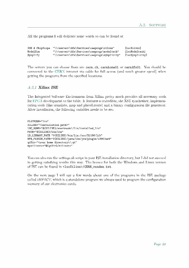
A.2. Software
All the programs I will dedicate some words to can be found at
ISE & ChipScope "\\<server>\dfs\Services\caeprogs\xilinx" [locXilinx]
ModelSim "\\<server>\dfs\Services\caeprogs\modeltech" [locModeltech]
Synplify "\\<server>\dfs\Services\caeprogs\synplicity" [locSynplicity]
The servers you can choose from are cern.ch, cernhome01 or cerndfs01. You should beconnected to the CERN intranet via cable for full access (and much greater speed) whengetting the programs from the specied locations.
A.2.1 Xilinx ISE
The Integrated Software Environment from Xilinx pretty much provides all necessary toolsfor FPGA development to the table. It features a texteditor, the XST synthesiser, implemen-tation tools (like translate, map and place&route) and a binary conguration le generator.After installation, the following variables needs to be set:
PLATFORM="lin"
XILINX="<installation path>"
LMC_HOME="$XILINX/smartmodel/lin/installed_lin"
PATH="$XILINX/bin/lin"
LD_LIBRARY_PATH="$XILINX/bin/lin:/usr/X11R6/lib"
NPX_PLUGIN_PATH="$XILINX/java/lin/jre/plugin/i386/ns4"
qtDir="<your home directory>/.qt"
myxilinxrc="$qtDir/xilinxrc"
You can also run the settings.sh script in your ISE installation directory, but I did not succeedin getting satisfying results this way. The licence for both the Windows and Linux versionof ISE can be found in <locXilinx>/CERN_readme.txt.
On the next page I will say a few words about one of the programs in the ISE packagecalled iMPACT, which is a standalone program we always used to program the congurationmemory of our electronics cards.
Page 80

A.2. Software
A.2.2 iMPACT
Impact is the software you have to use in order to program the Xilinx FPGAs7. ISE shouldalso be able to do this, but as Impact is made for the single purpose of programming FPGAsand conguration devices it became my preferred choice. Since programming the congura-tion devices is a task I encountered quite often - and no good tutorial was ever made on howto do it - I will try to give a simple and direct explanation on how to do it here 8.
• iMPACT Project is the title of the pop-up window you should get when launchingiMPACT. Select create a new project (.ipf) and hit OK.
• iMPACT - Welcome to iMPACT is the title of the next window you will get. SelectPrepare a PROM File and click Next.
• iMPACT - Prepare PROM Files. Check that I want to target a... is set to Xilinx
PROM, PROM File Format... is set to MCS, and Checksum Fill Value (2 Hex Digits)...is set to FF. Finally you need to ll the PROM File Name... eld, and set the locationto where you want the MCS le stored. When done, hit Next.
• iMPACT - Specify Xilinx PROM Device. Make sure the Select a PROM (bits)...leftmost rolldown box says xcf, and the rightmost rolldown box contains the name ofthe conguration device you want to program9. When these boxes are set hit Add.Make sure all the checkboxes on this page are unchecked, and click Next.
• iMPACT - File Generation Summary. Verify the settings and click Finish.
A small pop-up box informs you that you should now adding les to the project. Click OK,then select the .bit le you want to program the conguration device with. Answer NO tothe next box asking you whether you want to add more devices or not. Next doubleclick theow named Boundary Scan in the topleft Flows window. The main window should nowsay Right click to Add Device or Initialise JTAG chain. Do the latter and select the proper.bit le and .mcs le when confronted with this. In the same window you should now beable to see two icons, respectively representing the conguration device and the FPGA (seeg. A.1).
7Impact comes bundled with ISE8Approach may vary with software version. I used iMPACT version 9.2.04i.9The conguration device on the TRU are named xcf32p
Page 81

A.2. Software
Fig. A.1 - Screenshot of iMPACT
To start the programming procedure hit arrow tagged Program in the iMPACT Processeswindow. In the window that appears check the box reading Erase Before Programming
(under General CPLD And PROM Properties); likewise with the box labelled Load FPGA
(under PROM Specic Properties). All the other checkboxes I tend to leave unchecked.When done hit the OK button and the programming should commence.
When done you might want to save your project in order to just pick up the trace where youleft it the next time you are in need of ashing some conguration devices. This basicallywraps up my knowledge of this program. I simply found an approach that works, and keptdoing it that way. Feel free to explore.
Page 82

A.2. Software
A.2.3 ChipScope
The ChipScope Pro is a JAVA based application which allows you to analyse FPGA logic,various buses and even provides a function for making virtual inputs/outputs. While theChipScope Pro core are optimised for size and performance and are designed to operate atspeeds up to 200 MHz in Virtex-II Pro FPGAs, caution should be taken when speeds exceed150 MHz or logic usage exceed 80%. The ChipScope core uses some logic and a fair bitof Distributed SelectRAM (see 2.1.2.4). However, in our TRU/TOR designs the ChipScopecore will never driven at these speeds. This means we should be ne as long as the ChipScopecores are not made too big.
TopModule
ICONIntegrated Controller
control1 VIOVirtual
Input/Output
ILAIntegrated Logic
Analyser
Rest of the Design
con
trol0
sync_o
ut
sync_in
trig0
ChipScope Pro
JTAG
Fig. A.2 - ChipScope Principle [sofPPT]
For a complete tutorial on ChipScope I suggest looking into this one [docXCSTT].
ChipScope can be used to program FPGAs, but can not program the conguration devices.This means that the FPGA will keep its conguration until it is powercycled, when it willbe reprogrammed with the data in the conguration memory.
I was never able to get the drivers for the Xilinx USB programmer dongle to work underLinux. While I know that this is doable I did not care to bother with it as PHOS has alaptop dedicated to the task of programming electronics (it runs Windows XP). I used theCERN Desktop for transferring les between my private laptop and the PHOS laptop10.
[ 11 ]
10The path for a user specic CERN Desktop is:\\cern.ch\dfs\Users\<first letter of username>\<username>\Desktop
11Based on Based on [docXCJ50, page 54],[docXCSTT].
Page 83

A.2. Software
A.2.4 ModelSim
First, if you are installing ModelSim on a private computer you will need to set up a fewvariables.
PATH="<installation path>/modeltech/linux"
MGLS_LICENSE_FILE="[email protected]:[email protected]:[email protected]"
It is important to put the location of all the binaries in your PATH to get full interoperabilityfor ISE, ModelSim and Synplify. Especially the compilers start to misbehave if the binariesare not in you PATH variable. The licence is oating here at CERN, which means thereare CERN servers handing them out. The above licences work for both Linux and Windowsversions of ModelSim.
When you have ModelSim up and running, you have to perform some initial procedures:
• Clean Start. If you have simulated your project with ModelSim before, you yourself afavour and head over to your project location and delete the old work library (folder),the modelsim.ini le, and the <projectname>.mpf before doing anything else. I amnot sure why, but my ModelSim has a tendency to mess up badly if I skip this step.
• Set Project Directory. File I Change Directory....
• Create Working Library. File I New I Library.... Use default library name work,check that a new library and a logical mapping to it is selected and hit OK.
• Create the Project. File I New I Project.... Select a proper name for it, checkthat the project location is set right and make sure work is set as the default library.Do not copy settings from a previous modelsim.ini le, as we want to start blank inorder to know things are under control. Make sure that eld is blank, and that theoption for copying library mappings is checked. When done, hit OK.
• Add items to the Project. This is the label of the window appearing after you createdthe project. You may want to start making some folders to set up a hierarchy. Whenadding les I suggest you choose to reference to your les instead of copying them (atleast I want it to simulate my source les and not some backup I made).
Page 84

A.2. Software
When this is all done, you will need to compile the les the ModelSim way and add themto a simulation. This is best accomplished by using a .do le. It is more reliable, muchquicker and features a wide variety of options for customising the simulation to better suityour preferences.
quit -sim #Quit any old simulation you may have got running.
vlog +acc -sv TopModule.v #Compilation of the files you might have.
#(-acc = detailed transcript -sv = SystemVerilog)
vsim work.TopModule #Start the simulation
radix hex #I prefer the default radix to be hex
formatTime +commas +bestunits #I also prefer the use of "scientific units"
add wave -label <name> <ModuleName>=<SumModuleName>=<SignalName>
run 15 us #Simulation length
view wave #Show the wave window.
The compiler will probably complain about it not being able to nd the Xilinx primitives youhave used throughout your code. However, Xilinx has been so kind as to provide moduleswhich will behave the same way as the primitives when they are run in simulation. Get theones you need and copy them into your project (say, into a folder labelled primitives).
<ISE installation path>/verilog/src/unisims/ #High level modules.
<ISE installation path>/verilog/src/XilinxCoreLib/ #Low level components.
Some other documents you should read
Get Started Tutorial <installation path>/modeltech/docs/pdfdocs/modelsim_se_tut.pdf
UserManual <installation path>/modeltech/docs/pdfdocs/modelsim_se_user.pdf
Support for SystemVerilog <installation path>/modeltech/docs/technotes/sysvlog.note
Page 85

A.2. Software
A.2.5 Synplify
The Xilinx synthesiser called XST does a fairly good job, but Synplify is - in my opinion -far superior. What you do is open the source code les into Synplify (.v , .ngo , .edn
, .ucf), run the synthesis (this is the rst step of the implementation process) and noticethat .ngc/ngo les are created as output. There is a specic project type in ISE which hasthese letypes as basis, so you basically create one of these and let ISE do the rest of theimplementation after Synplify. After installation of Synplify, the following variables will needto be specied:
PATH="<installation path>/fpga_902/bin:<installation path>/identify_25/bin"
SYNPLICITY_LICENSE_FILE="1709@licman3:1709@licman2:1709@licman1"
Also these licences seem to work awlessly on both Linux and Windows operating systems.
When you wish to start using Synplify on a new project there is a small trick I use toget started quicker. First load up ISE with the project you want you synthesise, then setyour synthesiser to be Synplify (Pro). Run the synthesis once to get ISE to hand alongsome parameters to the Synplify project that will be made 12. Once done (it does not matterwhether the synthesis succeeded or failed) close ISE and start up Synplify (Pro). Have it openthe Synplify project which is now located in your project directory, and hit ImplementationOptions -> Verilog. Check the box tagged SystemVerilog and accept the changes. Voila,you are good to go!
12If you use Synplify version 9.0.1 it will always fail due to a bug that causes incompatibility between ISEand Synplicity
Page 86

A.3. Creating Backups
A.3 Creating Backups
When you are creating backups you need to know what les are important in your projectdirectory. If you simply copy it all you will end up with backups of several hundred MB,most of it being binaries from the implementation software which is not necessary to backup(as you can simply rerun the implementation to get them back). From starting a projectfrom scratch with a bare minimum of les, I have found that the only important les weneed to backup are:
*.v Verilog Source Code Files (The designer should know which are important)
toplevel.ucf The constraints file for the design
TopModule.ise The ISE Project File
*.ngo \& *.ngc Presynthesised code, or "black boxes". TopModule.ngc not needed.
The rest are just software generated les. If you ever run into problems where the softwareyou use does not seem to catch changes, then delete all les not mentioned above. This willstrip the design down to a absolute scratch, and force the programs to start all over with thesource les.
#! /bin/bash
cd <project path>/Backups #Assumes a "Backups" folder exist
mkdir $1 #Create the directory to store the data
cp ../*.v $1 #Copy all the Verilog source files,
cp ../*.ucf $1 #the .ucf constraints file,
cp ../TRURevised.ise $1 #the ISE project file,
cp ../*.bit $1 #the .bit file (used to program the FPGAs),
cp ../*.ngo $1 #all .ngo and
cp ../*.ngc $1 #.ngc files (presynthesised modules)
rm $1/TopModule.ngc #except this one which is created by ISE,
cp -r ../TriggerOut $1 #and finally all the files for TriggerOut,
cp -r ../BoardController $1 #BoardController and
cp -r ../Clk $1 #Clk.
Page 87

A.4. DCS Interfacing
A.4 DCS Interfacing
A.4.1 Via Ethernet
The easiest way to connect to a DCS card is if it is connected to the CERN intranet. Thenit will be assigned an IP-address from a CERN router (via DHCP), and you can access it byusing this IP or by using the name of the card (which will be translated to the IP-address withthe CERN DNS (Dynamic Name Server) service). Look at g. A.3 to see which DCS cardswere used in ALICE. In addition to these cards, I also interfaced a DCS card situated on aTOR development board (called pcdcstor2), and a DCS card situated on RCU developmentboard (called pcdcs0002). If the DCS cards are not connected to the CERN network theywill use an IP-address specied in the /etc/network le. Often this IP-address can be foundwith the following method:
10.1. (DCS number.>256)?1:0 . (DCS number.>256)?DCS number-256:DCS number
For instance, DCS number 279 (called alphdcs0279 on the network) would have IP-address:
10.1.1.(279-256) = 10.1.1.23
While other methods for addressing are used in ALICE, the method mentioned here was usedfor the DCS cards prior their installation in the ALICE detector.
If you know the local IP-address of a DCS card you can connect to directly with yourcomputer, or to via a router. You just have to make sure that you manually set the IP-address of your computer such that it is on the same subnet as the DCS card you want toaccess. For instance, if you want to access a DCS card with the IP-address 10.1.1.23, youshould set your computer up with for instance the IP-address 10.1.1.10. Now you can connectwithout problems.
When you connect to the DCS card with the IP-cable (SEMTEC connector), make sure thatthe red Light Emitting Diode (LED) starts to blink. This indicates that the communicationis up and running. If nothing happens, try to powercycle the +4.2V power supply. This is acommon problem and is caused by a bug in the DCS rmware (the bug is known, but is notyet corrected).
Page 88

A.4. DCS Interfacing
A.4.2 Via Serial Line
You can also connect to the DCS cards over the serial line (RS232 protocol). Fire up anyprogram that can deal with this for you (for instance the HyperTerminal application in MSWindows) and connect with the following settings:
COM Port ........ 1
Baud Rate ....... 57600
Data Bit ........ 8
Stop Bit ........ none
Parity .......... none
In my experience it is best if you try to connect straight after you rebooted the DCS card(either via. typing the command reboot or by powercycling the +4.2V power supply).
A.4.3 Set Up NFS Shares
NFS shares are folders which are physically present only on a host, but can be mounted intothe lesystem of other devices on the network (such as the DCS cards). Using this methodwith the DCS cards enables them to access lots of storage space even if they only have a fewMB of local memory.
To get started the computer need to have a NFS server up and running (see A.1), whichshould the the out-of-the-box case for most Linux distributions (distros). If not, they areeasy to set up. When the server is up, share (or export) the folder you wish to share (shouldalso be pretty self-explanatory). The computer is now ready.
The DCS cards are already ready for mounting NFS folders. The command used to do thisis listed below:
/usr/local/sbin/nfsmount <computer name>:<path to folder> <path to local folder> rw
The computer name can be either an IP-address or a DNS address, and the rw switch simplyindicates that the folder should be both readable and writeable. If you want the DCS cardto attempt to mount your folder every time it starts up place the mount command in thele:
/usr/local/sbin/nfsmount_all
It is surprisingly easy to do this, and it works surprisingly well.
Page 89

A.5. RJ45 Standard
A.4.4 Connecting to DCS in ALICE
Even when the PHOS module is in the ALICE cavern and none of the DCS cards are publiclyavailable on the CERN network, there is a way to remotely communicate with them. Youhave to be added in the PHS (short for PHOS) security group, and when you are you willbe able to login to a controlnode called alidcscom001.cern.ch via MS Windows RemoteDesktop Connection13. The mentioned node runs a Windows operating system, so to getfrom there to the DCS cards (which runs Linux) you need to use a program called Putty.Putty provides a SSH interface for use with Windows.
You might also wish to transfer les from and to the DCS cards, which you can use a programcalledWinSCP for. For letransfer between the alidcscom001 node and your own computer,use the DFS Desktop:
cern.ch I dfs I Users I <first letter of username> I <username> I Desktop
When the PHOS module was installed in the ALICE detector the DCS cards were allo-cated dierent names than they had on the CERN network. The current14 names of thevarious DCS cards can be looked up in g. A.3, along with a summary of what I have justmentioned.
Z
X
alidcsdcb1587
alidcsdcb1586
alidcsdcb1584
alidcsdcb1585
alidcsdcb1572
Transfer files via DFS Desktop
Remote login with MS Remote Desktop
Connection
alidcscom001.cern.ch
Transfer files with WinSCP
Terminal login with Putti
Fig. A.3 - Communication Flow when Remote Controlling DCS in ALICE [sofPPT]
13MS Windows Remote Desktop Connection should be a part of the bundled software that comes with mostWindows installations.
14As of 5.July 2008
Page 90
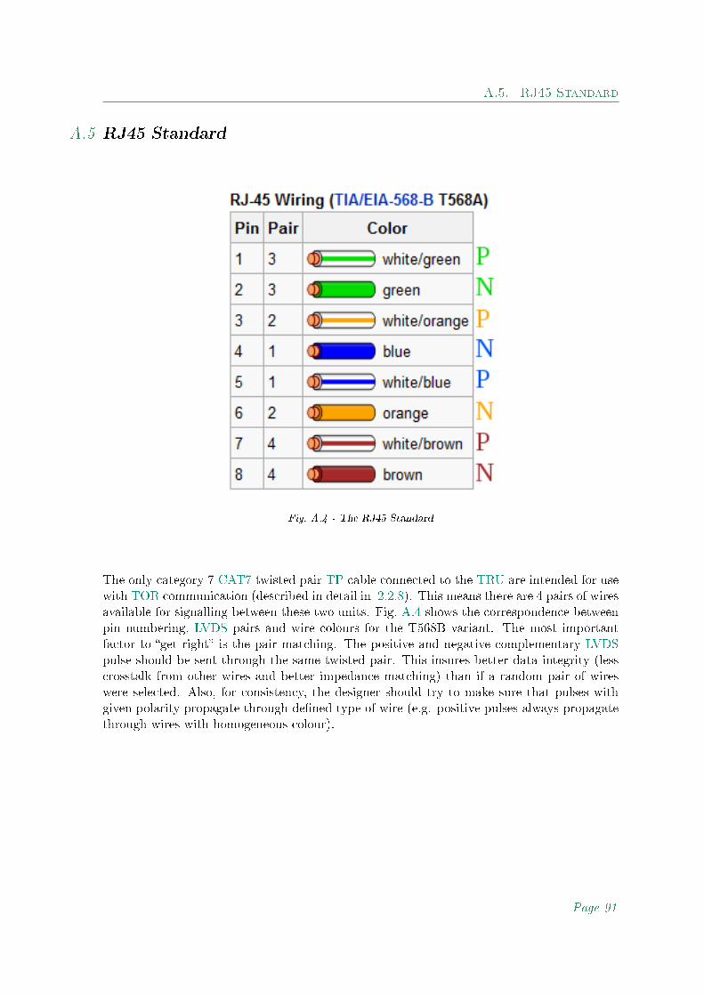
A.5. RJ45 Standard
A.5 RJ45 Standard
Fig. A.4 - The RJ45 Standard
The only category 7 CAT7 twisted pair TP cable connected to the TRU are intended for usewith TOR communication (described in detail in 2.2.8). This means there are 4 pairs of wiresavailable for signalling between these two units. Fig. A.4 shows the correspondence betweenpin numbering, LVDS pairs and wire colours for the T568B variant. The most importantfactor to get right is the pair matching. The positive and negative complementary LVDSpulse should be sent through the same twisted pair. This insures better data integrity (lesscrosstalk from other wires and better impedance matching) than if a random pair of wireswere selected. Also, for consistency, the designer should try to make sure that pulses withgiven polarity propagate through dened type of wire (e.g. positive pulses always propagatethrough wires with homogeneous colour).
Page 91

A.6. Adjusting the TRU ADC Clocks
A.6 Adjusting the TRU ADC Clocks
Test procedure for adjusting the bit- and frameclock for synchronising ADC data:
1. 0x0040 I 0x7c - Sample[3:0] = 4'h00x0050 I 0x7c - Sample[7:4] = 4'h00x0064 I 0x7c - Sample[11:8]= 4'h40x000c I 0x7c - Launch pattern, 3.5mA
This sets the ADCs up to output 1 on Sample[10]. Note what channel is showingthis bit.
2. 0x0040 I 0x7c - Sample[3:0] = 4'h00x0050 I 0x7c - Sample[7:4] = 4'h00x0068 I 0x7c - Sample[11:8]= 4'h80x000c I 0x7c - Launch pattern, 3.5mA
This sets the ADCs up to output 1 on Sample[11]. Did this 1 appear on the correctchannel (the more signicant than the previous one)? Yes (4). No (3).
3. 0x0005 I 0x7b - Add 45 to ADC_LCLK
See if the bits swap places. Keep adding 45 till they do.
4. 0x0010 I 0x79 - Add 22.5to ADC_ADCCLK
See how the MSB move. Keep adding 22.5 till its on Ch11.
You have now successfully tuned the bit- and frameclock to roughly the correct spot. Byperforming small phaseadjustments while watching the samples generated you may nd thegolden eye to clock each ADC channel.
If the samples are stable over time but the bits are correctly placed the frameclock is badlyadjusted. When samples vary over time either clock (or both) may be incorrectly adjusted,but chances are the bitclock is the sinner.
Page 92
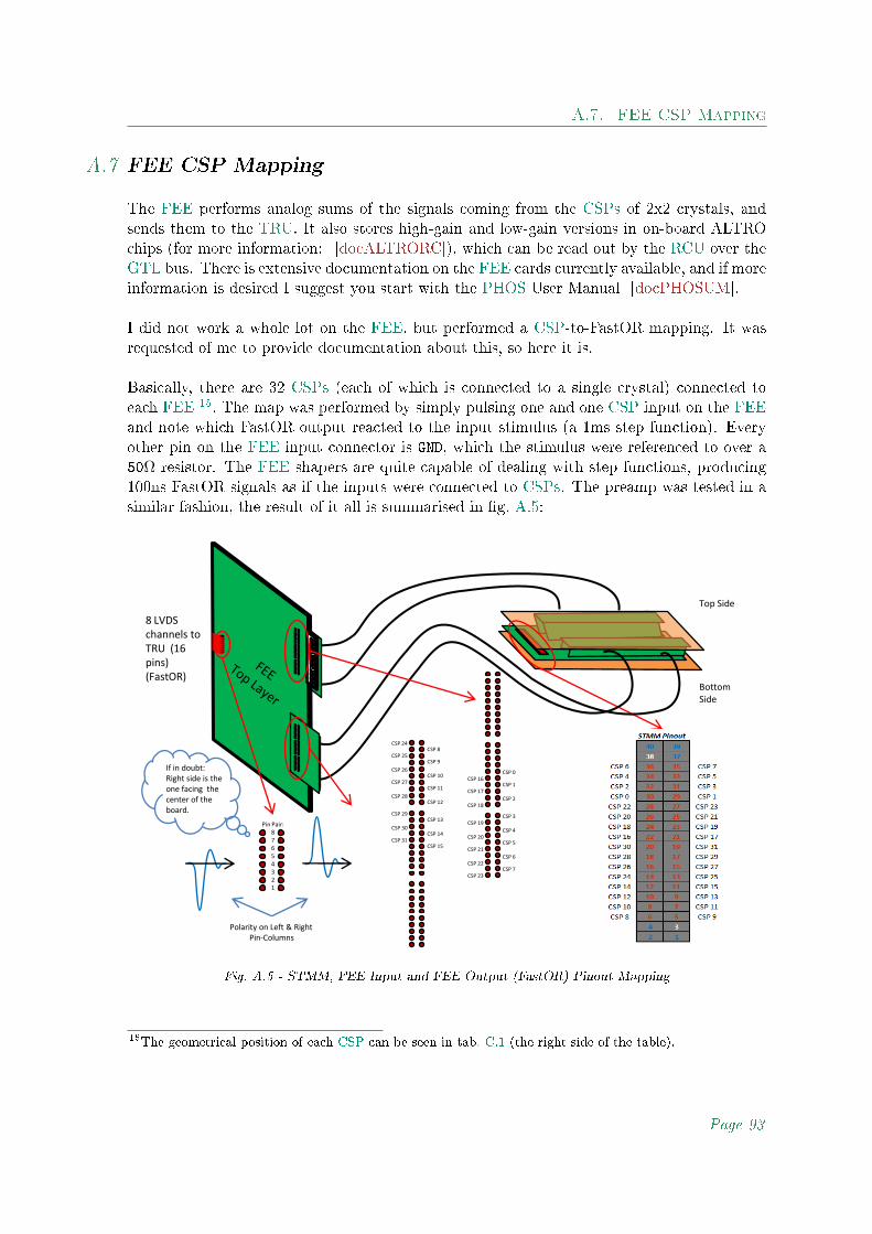
A.7. FEE CSP Mapping
A.7 FEE CSP Mapping
The FEE performs analog sums of the signals coming from the CSPs of 2x2 crystals, andsends them to the TRU. It also stores high-gain and low-gain versions in on-board ALTROchips (for more information: [docALTRORC]), which can be read out by the RCU over theGTL bus. There is extensive documentation on the FEE cards currently available, and if moreinformation is desired I suggest you start with the PHOS User Manual [docPHOSUM].
I did not work a whole lot on the FEE, but performed a CSP-to-FastOR mapping. It wasrequested of me to provide documentation about this, so here it is.
Basically, there are 32 CSPs (each of which is connected to a single crystal) connected toeach FEE 15. The map was performed by simply pulsing one and one CSP input on the FEEand note which FastOR output reacted to the input stimulus (a 1ms step function). Everyother pin on the FEE input connector is GND, which the stimulus were referenced to over a50Ω resistor. The FEE shapers are quite capable of dealing with step functions, producing100ns FastOR signals as if the inputs were connected to CSPs. The preamp was tested in asimilar fashion, the result of it all is summarised in g. A.5:
CSP 16
CSP 17
CSP 18
CSP 19
CSP 20
CSP 21
CSP 22
CSP 23
CSP 0
CSP 1
CSP 2
CSP 3
CSP 4
CSP 5
CSP 6
CSP 7
CSP 24
CSP 25
CSP 26
CSP 27
CSP 28
CSP 29
CSP 30
CSP 31
CSP 8
CSP 9
CSP 10
CSP 11
CSP 12
CSP 13
CSP 14
CSP 15
Top Side
Bottom Side
Pin Pair:87654321
Polarity on Left & Right Pin-Columns
If in doubt: Right side is the one facing the center of the board.
8 LVDS channels to TRU (16 pins)(FastOR)
Fig. A.5 - STMM, FEE Input and FEE Output (FastOR) Pinout Mapping
15The geometrical position of each CSP can be seen in tab. C.1 (the right side of the table).
Page 93

BChronograms
The chronograms shows the responses of some of my designs when they underwent simulationin Modeltech ModelSim. The testbenches used to create stimuli to the design inputs are men-tioned in 2.2.9. The signal names are the same as in the design code (see [srcTRUDESIGN]),so unless you have a look this aswell the chronograms will probably seem cryptic to you.If you just wanted to have a quick look then consider them a technological preview of thewaveform function in ModelSim.
Page 94

Fig. B.1 - The Process of Updating the ADCs with new Data Page 95

Fig. B.2 - First Stage of Deserialisation - Sorting the Bits [sofSIM]
Page 96

Notice
thephased
ieren
ceof
input/o
utputclo
cks:
ADC_LCLK
with
0tap
sof
phasesh
ift=0ps
ADC_LCLK
with
16tap
sof
phasesh
ift=260p
s
ADC_ADCCLKwith
0tap
sof
phasesh
ift=0ps
ADC_ADCCLKwith
16tap
sof
phasesh
ift=1660p
s
Theratio
260ps/1660p
s≈
TA
DC_
LC
LK/T
AD
C_
AD
CC
LK,andafullperio
dwill
beshifted
at255
taps.
Fig. B.3 - Synchronising ADC Inputs with DCM [sofSIM]
Page 97

CTRU Communication
In this attachment I will describe the various TRU registers currently1 available for the TRU.However, as a starting point I will show a few scripts I made in BASH which makes the taskof communicating with the TRU pretty easy.
I will use the ALICE ReadOut protocol (ALTRO)2 for this, although communication canalso be done via the low-speed serial lines (slow control)3. While these are BASH scripts,my two C++ programs (the DCS Oine Control Utility and TRU Register Scanner) haveboth slow control and ALTRO functionality implemented, see 4 for a description of theseprograms. I also implemented the ALTRO protocol in my TRU Testbench, as a means tovalidate the GTL controller (see 2.2.9).
The registers listed here comes straight from the code, but has been trimmed down quite a bitsince earlier versions of the code. The reason for this is that several registers were addressingfunctionality that is no longer present, or - if present - has been rendered redundant due toa change in design.
1Register list as of 30. June 20082For more information about the ALTRO protocol, take a look at the ALTRO User Manual [docALTROUM]and the RCU Firmware Manual [docRCUFM].
3See RCU Firmware Manual for more information about the slow control protocol [docRCUFM]. Thiscommunication protocol does not work very well with the TRU yet.
Page 98

C.1. Reading from the TRU
C.1 Reading from the TRU
Make a scriptle on the DCS card (or in a folder mounted on the DCS card) - say <path to
file>/ReadFromTRUReg.sh and put the following text in it:
#! /bin/bash
if [ $# -ne 2 ]; then
echo 1>&2 "Usage: $0 <register> <branch>"
echo 1>&2 "Example: $0 72 a"
echo 1>&2 "Read the register 72 on branch a"
exit 127
fi
branch=""
if [ $2x = "ax" ]; then
branch=2
fi
if [ $2x = "bx" ]; then
branch=3
fi
if [ $branchx = "x" ]; then
echo 1>&2 "Not a valid branch!"
exit 127
fi
rcu-sh w 0x7000 0x5$branch00$1 #Setup address to read from.
rcu-sh w 0x0 0x300000 #Set stop flag.
rcu-sh wait 1 us
rcu-sh r 0x7800 #Read ErrorStatus Register
rcu-sh wait 1 us
rcu-sh r 0x6000 1 #Output the value read back*
Now call the command - e.g. do <path to file>/ReadFromTRUReg.sh 72 a - and see whatvalue register 0x072 (which holds the value for the Global Level0 Threshold) on branch a
contained.
If you really want to know what all these commands do, feel free to look it up in the ALTROUser Manual [docALTROUM] or in the PHOS User Manual [docPHOSUM].
Page 99

C.2. Writing to the TRU
C.2 Writing to the TRU
Make a scriptle on the DCS card (or in a folder mounted on the DCS card) - say <path to
file>/WriteToTRUReg.sh and put the following text in it:
#! /bin/bash
if [ $# -ne 3 ]; then
echo 1>&2 "Usage: $0 <value> <register> <branch>"
echo 1>&2 "Example: $0 00ff 72 a"
echo 1>&2 "Write the value ff to TRU register 72 on branch a"
exit 127
fi
branch=""
if [ $3x = "ax" ]; then
branch=2
fi
if [ $3x = "bx" ]; then
branch=3
fi
if [ $branchx = "x" ]; then
echo 1>&2 "Not a valid branch!"
exit 127
fi
rcu-sh w 0x6c01 0x0 #Clear the Error Status Flag
rcu-sh w 0x7000 0x6$branch00$2 #Setup address to write to.
rcu-sh w 0x7001 0x70$1 #Setup data to write.
rcu-sh w 0x7002 0x5$branch00$2 #Setup address to read from.
rcu-sh w 0x7003 0x390000 #Set stop flag.
rcu-sh wait 10 us
rcu-sh w 0x0 0x300000 #Execute
rcu-sh wait 10 us
rcu-sh r 0x7800 #Read ErrorStatus Register
rcu-sh wait 10 us
rcu-sh r 0x6000 1 #Output the value read back*
if [ $# -ne 3 ]; then
echo 1>&2 "Usage: $0 <value> <register> <branch>"
echo 1>&2 "Usage: $0 <value> <register> <branch>"
echo 1>&2 "Example: $0 00ff 72 a"
echo 1>&2 "Write the value ff to TRU reguster 72 on branch a"
exit 127
fi
Now call the command - e.g. do <path to file>/WriteToTRUReg.sh 00ff 72 a - and ndthat the value 0x00ff was written to TRU register 0x072 on branch a (which holds the valuefor the Global Level0 Threshold).
Page 100

C.3. Register List
C.3 Register List
In case you wonder, these registers should be the same as the ones being scanned if you areusing my TRU Register Scanner (see 4.5). The format is as follows:
<register address> [design name] <'R'ead-only or 'R'ead/'W'rite> <A short description>
Temperature, Voltage and Current Sensors0x01 [T1_TH] R/W Maximum Temperature
0x02 [A4V0_TH] R/W Min. 4V Ana. Voltage
0x03 [A4V0C_TH] R/W Max. 4V Ana. Current
0x04 [D4V2_TH] R/W Min. 4.2V Dig. Voltage
0x05 [D4V2C_TH] R/W Max. 4.2V Dig. Current
0x06 [TEMP1] R Temperature Value ( decimal value/4 = temperature
0x07 [A4V0] R 4V Analogue Voltage Value
0x08 [A4V0C] R 4V Ana. Current Value
0x09 [D4V2] R 4.2V Dig. Voltage Value
0x0a [D4V2C] R 4.2V Dig. Current Value
Interrupt registers0x11 [CSR0] R Interrupt - Mask Register
0x12 [CSR1] R Error Status Register
Fake ALTRO register0x1A [CHRDO] W Channel ReadOut (Fake ALTRO register)
Note: This is not a BC register!
The TRU retains a history of 256 samples (or 256*40MHz = 6.4µs) in Block Select RAM(which is pedestal corrected), of which the 10 last samples (250ns) may be read as triggerdata type 1. This is what the Fake ALTRO readout mechanism are for.
Consult the PHOS User Manual [docPHOSUM, page 102] for the ALTRO protocol dataformat.
Important! When the ALTRO Readout command are executed the RCU are addressing theALTRO chips (which are located on the FEE cards, see [docPHOSUM] for more information).This means that my example script can not be used to launch this command (branchnumbers must be changed from 2 and 3 to 0 and 1, respectively). Also, an extension in theTRU BoardController will be needed here in order not to ignore this command as an ALTROrequest (a command is either a BoardController or ALTRO request, never both).
Firmware revision0x20 [BC_VER] R Version of BoardController
Page 101

C.3. Register List
Temperature, Voltage and Current Sensors
0x21 [T2_TH] R/W Maximum Temperature
0x22 [D3V3_TH] R/W Min. 3.3V Dig. Voltage
0x23 [D3V3C_TH] R/W Max. 3.3V Dig. Current
0x24 [D2V5_TH] R/W Min. 2.5V Dig. Voltage
0x25 [D1V5_TH] R/W Min. 1.5V Dig. Voltage
0x28 [TEMP2] R Temperature Value ( decimal value/4 = temperature)
0x29 [D3V3] R 3.3V Dig. Voltage Value
0x2a [D3V3C] R 3.3V Dig. Current Value
0x2b [D2V5] R 2.5V Dig. Voltage Value
0x2c [D1V5] R 1.5V Dig. Voltage Value
0x2e [ADC_ID] R Temp./Voltage Sensor ID
0x2f [TEST_REG] ? Test Register???
Auxiliary Interrupt registers for Monitoring (not clear if we need these)
0x65 [VTS] bits to be re-allocated for TRU Aux. Interrupt Flag register
0x66 [INT_MASK] bits to be re-allocated for TRU Interrupt mask
Hardware Versions
0x70 [CARD_NO] R TRU board version ( Current is 2.0 )
0x71 [SER_NO] R TRU serial Number ( just upcounting )
Global Level0 Threshold
0x72 [GTHR_L0] R/W L0 Global Threshold
This threshold only applies for those 4x4 which has a local 4x4 threshold set to a valueunequal to 0, see the registers 0xa5 to 0xff.
TOR Readout Sync
0x78 [TORSYNC] R/W Relative bunch number register (8 bits)
The TOR will receive 14 bit time-summed data which are stored in Block Select RAM (sincethese are huge a history of 256 samples will be retained). The plan is to use this register tospecify the position of the data in the RAM block to neadjust what data the TOR receives.The position will be relative to position of peak which will be internally stored for the lastLevel0 produced.
The rst bunch will arrive at the TRU ≈350ns after beam crossing (particle collision). After580ns the Level0 must be produced and so the necessary history to store is 580ns350ns =230ns- which translates to roughly 10 samples.
Page 102

C.3. Register List
ADC Deserialiser Sync
0x79 [ADCoutSYNC] R/W Value 0..511 - PhaseShift for DCM sourcing "frameclock"
0x7a [ADCinSYNC] R/W Value 0..511 - PhaseShift for DCM sourcing "bitclock"
Refer to attachment A.6 for instructions on how to use these registers.
ADC Control Register
0x7c [ADCCONTROL] R/W ADC serial data pattern (ADS5270 data sheet)
ADDRESS DATA DESCRIPTION REMARKS
D7 D6 D5 D4 D3 D2 D1 D0 All Data Outputs
0 0 0 0 LVDS Buers0 0 Normal ADC Output (default after reset)0 1 Deskew Pattern *1 0 Sync Pattern *1 1 Custom Pattern *
0 0 IOUT LVDS ≈ 3.5mA (default after reset)0 1 IOUT LVDS ≈ 2.5mA1 0 IOUT LVDS ≈ 4.5mA1 1 IOUT LVDS ≈ 6.0mA
0 0 0 1 CLOCK CURRENT0 X X 0 LVDS Clock Output Current IOUT ≈ 3.5mA(default)0 X X 1 2x LVDS Clock Output Current IOUT ≈ 7.0mA
0 0 0 1 LSB/MSB MODE0 0 X X LSB First Mode (default after reset)0 1 X X MSB First Mode
0 0 1 0 POWER DOWN ADC CH.X X X X Power-Down Ch. 1 to 4.
D3 = Ch.4, D0 = Ch.1
0 0 1 1 POWER DOWN ADC CH.X X X X Power-Down Ch. 5 to 8.
D3 = Ch.8, D0 = Ch.5
CUSTOM PATTERN0 1 0 0 X X X X *0 1 0 1 X X X X *0 1 1 0 X X X X *
* Take a look at tab. C.2
Tab. C.1 - Commandwords you can send to the ADC [docADC][Page 6]
Serial Output LSBADC Output D0 D1 D2 D3 D4 D5 D6 D7 D8 D9 D10 D11
Deskew Pattern 1 0 1 0 1 0 1 0 1 0 1 0Sync Pattern 0 0 0 0 0 0 1 1 1 1 1 1
Custom Pattern D04 D14 D24 D34 D05 D15 D25 D35 D06 D16 D26 D36
Tab. C.2 - Description ADC Patterns [docADC][Page 6]
Page 103
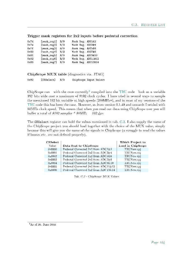
C.3. Register List
Trigger mask registers for 2x2 inputs before pedestal correction
0x7d [mask_reg1] R/W Mask Reg. ADC1&2
0x7e [mask_reg2] R/W Mask Reg. ADC3&4
0x7f [mask_reg3] R/W Mask Reg. ADC5&6
0x80 [mask_reg4] R/W Mask Reg. ADC7&8
0x81 [mask_reg5] R/W Mask Reg. ADC9&10
0x82 [mask_reg6] R/W Mask Reg. ADC11&12
0x83 [mask_reg7] R/W Mask Reg. ADC12&14
ChipScope MUX table (diagnostics via. JTAG)
0x92 [CSSelect] R/W ChipScope Input Select
ChipScope can - with the core currently4 compiled into the TRU code - look at a variable192 bits wide over a maximum of 8192 clock cycles. I have tried in several ways to samplethe mentioned 192 bit variable at high speeds (200MHz+), and in most of my versions of theTRU code this has been the case. However, as from version 0.1.49 and onwards I settled with80MHz clock speed. This means that when you read out data using ChipScope now you willbuer a total of 8192 samples * 80MHz = 102.4µs
The CSSelect register can hold the values mentioned in tab. C.3. I also supply the name ofthe ChipScope project you should load together with the choice of the MUX value, simplybecause this will give you the name of the signals in ChipScope (a struggle to read the valuesif busses etc. are not dened properly).
CSSelect Which Project toValue Data Sent to ChipScope Load in ChipScope0x0000 Pedestal Corrected 2x2 from ADC1&2 TRUNew.cpj0x0001 Pedestal Corrected 2x2 from ADC3&4 TRUNew.cpj0x0002 Pedestal Corrected 2x2 from ADC5&6 TRUNew.cpj0x0003 Pedestal Corrected 2x2 from ADC7&8 TRUNew.cpj0x0004 Pedestal Corrected 2x2 from ADC9&10 TRUNew.cpj0x0005 Pedestal Corrected 2x2 from ADC11&12 TRUNew.cpj0x0006 Pedestal Corrected 2x2 from ADC13&14 TRUNew.cpj
Tab. C.3 - ChipScope MUX Values
4As of 30. June 2008
Page 104

C.3. Register List
Trigger threshold registers (91 instances)
0xa5
to [4x4Thr] R/W 4x4 local thresholds to space-time-sums (16 bit )
0xff
To get some impression of which of the addressed 4x4Thr registers applies to which geomet-rical 4x4 bunch of crystals, take a look at g. C.1.
Z
X
Channel FEE1 FEE2 FEE3 FEE4 FEE5 FEE6 FEE7 FEE8 FEE9 FEE10 FEE11 FEE12 FEE13 FEE14
CSPlocation:
10 161 17
22 183 19
34 205 21
46 227 23
58 249 25
610 2611 27
712 2813 29
814 3015 31
ADC1 ADC2 ADC3 ADC4 ADC5 ADC6 ADC7 ADC8 ADC9 ADC10 ADC11 ADC12 ADC13 ADC14
A5
A6
A7
A8
A9
AA
AB
AC
AD
AE
AF
B0
B1
B2
B3
B4
B5
B6
B7
B8
B9
BA
BB
BC
BD
BE
BF
C0
C1
C2
C3
C4
C5
C6
C7
C8
C9
CA
CB
CC
CD
CE
CF
D0
D1
D2
D3
D4
D5
D6
D7
D8
D9
DA
DB
DC
DD
DE
DF
E0
E1
E2
E3
E4
E5
E6
E7
E8
E9
EA
EB
EC
ED
EE
EF
F0
F1
F2
F3
F4
F5
F6
F7
F8
F9
FA
FB
FC
FD
FE
FF
Fig. C.1 - 4x4 Threshold Map [sofXLS]
Fig. C.1 depicts a branch of 14 FEE cards (the TRU sits in the middle but I left it out), seenalong the positive y-axis (that is, looking at the back of the PHOS module; the electronicslayer). FEEs are mapped to equally indexed ADCs on the TRU, and the FastOR channels toequally indexed ADC channels. The numbering increases along the positive axis' of x and z,respectively. On the right side of the table I attached the CSP numbering (charge sensitivepreampliers, one per crystal). This way you can now see which CSP are being mapped towhich 4x4, and which 4x4 threshold(s) that are aecting it.
Example: <path>/WriteToTRUReg.sh 00ff a5 a would write to the TRU on branch a. Youwrite to register a5 the value 0x00ff, which means that if the energy of CSP0,1,2,3,16,17,18,19from FEE1 and FEE2 combined exceeds the value 0x00ff then you have a level0. Remem-ber that you sum up the energy not only in space, but also in time. Also, what the number0x00ff actually represent in respect to energy is not yet clear.
Page 105

DTRU Logic Utilisation
This appendix simply shows a small selection of the MAP process summary (a part of theimplementation software in Xilinx ISE). They give an indication of the logical usage of theold versus the new TRU design, but should not be considered absolute as there are severalfactors that can aect them. First of all, the synthesiser, translate-, map- and place androute function can all introduce small variations to the nal distribution of logic. Only aminor change in the code can cause several domino-eects which makes these tools decideto go for a complete dierent set of logical elements. Especially true is this for designs thatconsumes an amount of logic which is close to the limit of resources available in the FPGA.Then the tools will start to nd ways to pack logic together and share common resourcesfabric, which makes it very hard to keep track of what sort of impact your change in designhad for the total level of resource usage.
Also, I have seen that the numbers change quite a lot between dierent versions of Xilinx ISE.From version 9.1 to version 10.1 the register usage reported by XST (Xilinx ISE Synthesiser)increased by about 5%, while the place and route tools reported about the same decrease.Both of the summaries below is therefore from an implementation with ISE 10.1.
The single most important reason why you should not compare the numbers listed heredirectly is that the old and the new design contains dierent functional elements. Some newfunctions were added, some old and redundant were removed, and a lot of the code wasrevised. These factors aside, please feel free to have a look if you are interested. Note thatthe new design uses less logic in general (the CLB usage is below the critical 90% level), andtakes only a fraction of the time to implement.
Page 106

D.1. Old Design
D.1 Old Design
Design Summary
--------------
Number of errors: 0
Number of warnings: 59
Logic Utilisation:
Total Number Slice Registers: 32,505 out of 47,232 68%
Number used as Flip Flops: 32,491
Number used as Latches: 14
Number of 4 input LUTs: 32,809 out of 47,232 69%
Logic Distribution:
Number of occupied Slices: 23,614 out of 23,616 99%
Number of Slices containing only related logic: 19,068 out of 23,614 80%
Number of Slices containing unrelated logic: 4,546 out of 23,614 19%
*See NOTES below for an explanation of the effects of unrelated logic.
Total Number of 4 input LUTs: 34,706 out of 47,232 73%
Number used as logic: 29,978
Number used as a route-thru: 1,897
Number used for 32x1 RAMs: 20
(Two LUTs used per 32x1 RAM)
Number used as Shift registers: 2,811
Number of bonded IOBs: 395 out of 692 57%
IOB Flip Flops: 5
IOB Master Pads: 118
IOB Slave Pads: 118
Number of TBUFs: 1 out of 11,808 1%
Number of RAMB16s: 130 out of 232 56%
Number of BUFGMUXs: 11 out of 16 68%
Number of DCMs: 6 out of 8 75%
Number of BSCANs: 1 out of 1 100%
Number of RPM macros: 15
Peak Memory Usage: 734 MB
Total REAL time to MAP completion: 12 mins 41 secs
Total CPU time to MAP completion: 12 mins 27 secs
Page 107
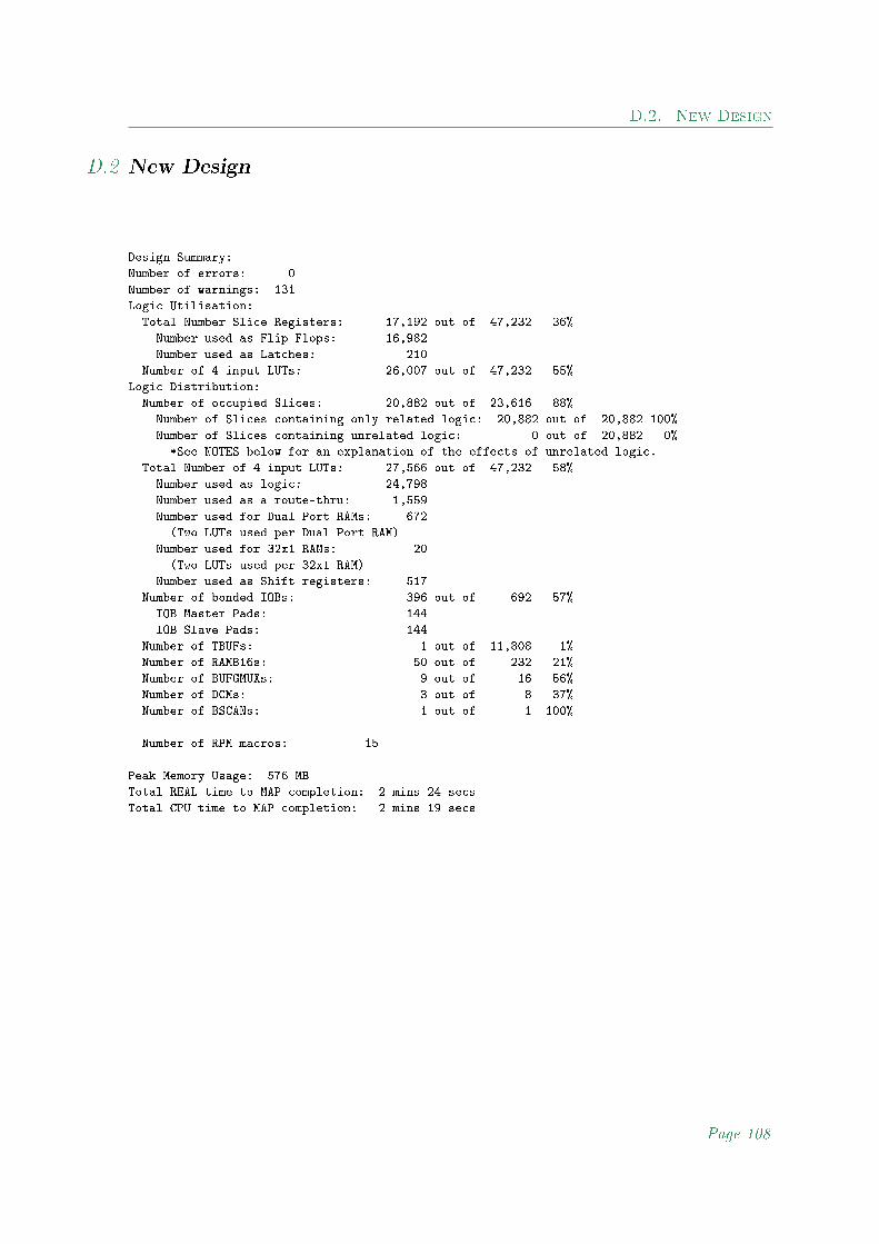
D.2. New Design
D.2 New Design
Design Summary:
Number of errors: 0
Number of warnings: 131
Logic Utilisation:
Total Number Slice Registers: 17,192 out of 47,232 36%
Number used as Flip Flops: 16,982
Number used as Latches: 210
Number of 4 input LUTs: 26,007 out of 47,232 55%
Logic Distribution:
Number of occupied Slices: 20,882 out of 23,616 88%
Number of Slices containing only related logic: 20,882 out of 20,882 100%
Number of Slices containing unrelated logic: 0 out of 20,882 0%
*See NOTES below for an explanation of the effects of unrelated logic.
Total Number of 4 input LUTs: 27,566 out of 47,232 58%
Number used as logic: 24,798
Number used as a route-thru: 1,559
Number used for Dual Port RAMs: 672
(Two LUTs used per Dual Port RAM)
Number used for 32x1 RAMs: 20
(Two LUTs used per 32x1 RAM)
Number used as Shift registers: 517
Number of bonded IOBs: 396 out of 692 57%
IOB Master Pads: 144
IOB Slave Pads: 144
Number of TBUFs: 1 out of 11,808 1%
Number of RAMB16s: 50 out of 232 21%
Number of BUFGMUXs: 9 out of 16 56%
Number of DCMs: 3 out of 8 37%
Number of BSCANs: 1 out of 1 100%
Number of RPM macros: 15
Peak Memory Usage: 576 MB
Total REAL time to MAP completion: 2 mins 24 secs
Total CPU time to MAP completion: 2 mins 19 secs
Page 108

EFascinating Facts
Please note that this is a copy-paste (with few edits) from [docLHCUG], but I put them inanyway since I found them to be a good read.
1. When the 27-km long circular LHC tunnel was excavated, between Lake Geneva andthe Jura mountain range, the two ends met up to within 1 cm.
2. Each of the 6400 superconducting laments of niobium-titanium in the cable producedfor the LHC is about 0.007mm thick, about 10 times thinner than a normal humanhair. If you added all the laments together they would stretch to the Sun and backve times with enough left over for a few trips to the Moon.
3. All protons accelerated at CERN are obtained from standard hydrogen. Although pro-ton beams at the LHC are very intense, only 2 nanograms of hydrogen are acceleratedeach day. Therefore, it would take the LHC about 1 million years to accelerate 1 gramof hydrogen.
4. The central part of the LHC will be the world's largest fridge. At a temperature colderthan deep outer space, it will contain iron, steel and the all important superconductingcoils.
5. The pressure in the beam pipes of the LHC will be about ten times lower than on theMoon. This is an ultrahigh vacuum.
6. Protons at full energy in the LHC will be travelling at 0.999999991 times the speed oflight. Each proton will go round the 27 km ring more than 11 000 times a second.
7. At full energy, each of the two proton beams in the LHC will have a total energyequivalent to a 400 t train (like the French TGV) travelling at 150 km/h. This isenough energy to melt 500 kg of copper.
8. The Sun never sets on the ATLAS collaboration. Scientists working on the experimentcome from every continent in the world, except Antarctica.
9. The CMS magnet system contains about 10 000 t of iron, which is more iron than inthe Eiel Tower.
10. The data recorded by each of the big experiments at the LHC will be enough to llaround 100 000 DVDs every year.
Page 109

List of Tables
2.1 TRU Components . . . . . . . . . . . . . . . . . . . . . . . . . . . . . . . . . 172.2 Virtex 2 Pro (XC2VP50) Specications [docV2PDS, page 2] . . . . . . . . . 182.3 Logic Provided by 1 Congurable Logic Block (CLB) [docV2PDS, page 52] . 202.4 TRU History [docNICOLAS, top part from page 88] . . . . . . . . . . . . . . 232.5 TRU External Clocks . . . . . . . . . . . . . . . . . . . . . . . . . . . . . . . 272.6 Deserialiser Logic Usage - Compared with Alans Deserialiser . . . . . . . . . . 42
3.1 Pulse Generator Registers . . . . . . . . . . . . . . . . . . . . . . . . . . . . . 61
4.1 PHOS Control Utility - Settings File . . . . . . . . . . . . . . . . . . . . . . . 664.2 TRU Register Scanner - Settings File . . . . . . . . . . . . . . . . . . . . . . . 704.3 TRU Register Scanner - Results File . . . . . . . . . . . . . . . . . . . . . . . 71
C.1 Commandwords you can send to the ADC [docADC][Page 6] . . . . . . . . . 103C.2 Description ADC Patterns [docADC][Page 6] . . . . . . . . . . . . . . . . . . 103C.3 ChipScope MUX Values . . . . . . . . . . . . . . . . . . . . . . . . . . . . . . 104
Page 110

List of Figures
1.1 What crazy scheme are we involved in? [imgEAS] . . . . . . . . . . . . . . . . 11.2 The Building Blocks of matter [docCERN] . . . . . . . . . . . . . . . . . . . 21.3 The CERN Globe [imgCGL] . . . . . . . . . . . . . . . . . . . . . . . . . . . . 41.4 Some Citations from the CERN Web Page [intCHP] [sofPPT] . . . . . . . . 41.5 The Large Hadron Collider Complex [intPRESS, Custom Tags] . . . . . . . . 51.6 The Accelerator Complex [docLHCUG] . . . . . . . . . . . . . . . . . . . . . . 61.7 The ALICE Detector [imgALIDET, Custom Tags] . . . . . . . . . . . . . . . 71.8 The Basic Buildup of a PHOS Module [sofPPT] [sofPSP] . . . . . . . . . . . 91.9 1 of the 8 Branches in the Electronics Layer [sofPPT] . . . . . . . . . . . . 10
2.1 TRU Position in a Branch of Front-End Cards [sofPPT] [sofGMP] . . . . . . 152.2 Front Side View of the Trigger Region Unit (TRU) [sofPSP] . . . . . . . . . 162.3 A Simplied Illustration of the Virtex 2 Congurable Logic Block (CLB)
[docV2PDS, page 45] [sofPPT] . . . . . . . . . . . . . . . . . . . . . . . . . . 192.4 Virtex 2 Pro Global Clock Distribution [docV2PUG, page 69] [sofPPT] . . . 212.5 TRU Code Buildup [sofPPT] . . . . . . . . . . . . . . . . . . . . . . . . . . . 242.6 ADC Interaction [sofPPT] . . . . . . . . . . . . . . . . . . . . . . . . . . . . 292.7 Noise Map of PHOS Module 2 [sofXLS] . . . . . . . . . . . . . . . . . . . . . 322.8 Synchronising the ADC Databits [sofPPT] . . . . . . . . . . . . . . . . . . . 332.9 Synchronising Bits and Frames [sofPPT] . . . . . . . . . . . . . . . . . . . . 342.10 Deserialisation Stage 1 - Serial Stream Decomposition [sofPPT] . . . . . . . . 402.11 Deserialisation Stage 2 - Deserialisation and Phase Correction [sofPPT] . . . 412.12 Level0 Trigger Generation [sofPPT] . . . . . . . . . . . . . . . . . . . . . . . 462.13 Design Suggestion for TRU-TOR Communication [sofPPT] . . . . . . . . . . 51
3.1 LVDS Input Buer [sofPPT] . . . . . . . . . . . . . . . . . . . . . . . . . . . 59
4.1 Current Supplied by the PHOS PowerSupply during Card-by-Card PowerUp[sofGMP] [sofPPT] . . . . . . . . . . . . . . . . . . . . . . . . . . . . . . . . . 68
A.1 Screenshot of iMPACT . . . . . . . . . . . . . . . . . . . . . . . . . . . . . . . 82A.2 ChipScope Principle [sofPPT] . . . . . . . . . . . . . . . . . . . . . . . . . . 83A.3 Communication Flow when Remote Controlling DCS in ALICE [sofPPT] . . 90A.4 The RJ45 Standard . . . . . . . . . . . . . . . . . . . . . . . . . . . . . . . . . 91A.5 STMM, FEE Input and FEE Output (FastOR) Pinout Mapping . . . . . . . 93
B.1 The Process of Updating the ADCs with new Data . . . . . . . . . . . . . . . 95B.2 First Stage of Deserialisation - Sorting the Bits [sofSIM] . . . . . . . . . . . . 96B.3 Synchronising ADC Inputs with DCM [sofSIM] . . . . . . . . . . . . . . . . . 97
C.1 4x4 Threshold Map [sofXLS] . . . . . . . . . . . . . . . . . . . . . . . . . . . 105
Page 111

Bibliography
[MyMind] Denately my greatest source of information.
Books
[bokAsh08] Peter J. Ashenden, Digital Design - An Embedded Systems Approach UsingVerilog, Morgan Kaufman (2008), ISBN:978-0-12-369527-7
Documents
[docAD7417] Temperature Sensorhttp: // www. joinge. net/ cern/ report/ bib/ AD7417. pdf
[docADC] TRU ADC (ADS5270)http: // www. joinge. net/ cern/ report/ bib/ ADC. pdf
[docADG774] Multiplexer/demultiplexerhttp: // www. joinge. net/ cern/ report/ bib/ ADG774. pdf
[docALICE] ALICE Brochure No. 2 2003http: // www. joinge. net/ cern/ report/ bib/ ALICE. pdf
[docALTRORC] ALTRO ReadOut Chip - IEEE Transactions on Nuclear ScienceVol. 50, No. 6, December 2003
http: // www. joinge. net/ cern/ report/ bib/ ALTRORC. pdf
[docALTROUM] ALICE ReadOut Protocol (ALTRO) User Manual June 2002http: // www. joinge. net/ cern/ report/ bib/ ALTROUM. pdf
[docAPA075] ProASIC Flash Memoryhttp: // www. joinge. net/ cern/ report/ bib/ APA075. pdf
[docCERN] CERN Brochure No. 2 2008http: // www. joinge. net/ cern/ report/ bib/ CERN. pdf
[docDAVID]
[docDAVID] David Koenigseders Activity Report φhttp: // www. joinge. net/ cern/ report/ bib/ DAVID. pdf
Page 112

Bibliography
[docGRID] GRID Brochure No. 2 2006http: // www. joinge. net/ cern/ report/ bib/ GRID. pdf
[docGTL] GTL Drivershttp: // www. joinge. net/ cern/ report/ bib/ GTL. pdf
[docLHC] LHC Brochure No. 2 2006http: // www. joinge. net/ cern/ report/ bib/ LHC. pdf
[docLHCUG] LHC The Ultimate Guide No. 1 2008http: // www. joinge. net/ cern/ report/ bib/ LHCUG. pdf
[docLSF] Olivier Bourrion - (TOR-TRU) Link Speed Feasability Test Report (rev.10/07/2007)
http: // www. joinge. net/ cern/ report/ bib/ LSF. pdf
[docLVDS101] LVDS Driverhttp: // www. joinge. net/ cern/ report/ bib/ LVDS101. pdf
[docLVDS31] LVDS Driverhttp: // www. joinge. net/ cern/ report/ bib/ LVDS31. pdf
[docLVDS32] LVDS Receiverhttp: // www. joinge. net/ cern/ report/ bib/ LVDS32. pdf
[docMAX6627] Temperature Sensorhttp: // www. joinge. net/ cern/ report/ bib/ MAX6627. pdf
[docMPC9109] Clock Distribution Chiphttp: // www. joinge. net/ cern/ report/ bib/ MPC9109. pdf
[docMX29LV] Flash memoryhttp: // www. joinge. net/ cern/ report/ bib/ MX29LV. pdf
[docNICOLAS] Nicholas Degrenne' Activity Report - 2007http: // www. joinge. net/ cern/ report/ bib/ NICOLAS. pdf
[docPHOSUM] PHOton Spectrometer (PHOS) User Manual - 4. January 2007(Hans Muller)
http: // www. joinge. net/ cern/ report/ bib/ PHOSUM. pdf
[docRCUFM] ReadOut Control Unit (RCU) Firmware Manual 18.December 2006http: // www. joinge. net/ cern/ report/ bib/ RCUFM. pdf
Page 113

Bibliography
[docSO2222] Power Supply Transistorhttp: // www. joinge. net/ cern/ report/ bib/ SO2222. pdf
[docTIMCLOS] Timing Closure Techniques (supplied by a Xilinx designer on theXilinx forums)
http: // www. joinge. net/ cern/ report/ bib/ TIMCLOS. pdf
[docTORDESIGN] TOR Design Sheethttp: // www. joinge. net/ cern/ report/ bib/ TORDESIGN. doc
[docTRU1.1] TRU Design Sheet v1.1http: // www. joinge. net/ cern/ report/ bib/ TRU1. 1. pdf
[docV2PDS] Virtex 2 Pro Datasheethttp: // www. joinge. net/ cern/ report/ bib/ V2PDS. pdf
[docVR15V] 1.5V Voltage Regulatorhttp: // www. joinge. net/ cern/ report/ bib/ VR15V. pdf
[docVR18V] 1.8V Voltage Regulatorhttp: // www. joinge. net/ cern/ report/ bib/ VR18V. pdf
[docVR25V] 2.5V Voltage Regulatorhttp: // www. joinge. net/ cern/ report/ bib/ VR25V. pdf
[docVR33BU] 3.3V Voltage Regulatorhttp: // www. joinge. net/ cern/ report/ bib/ VR33BU. pdf
[docVR33WU1] 3.3V Voltage Regulatorhttp: // www. joinge. net/ cern/ report/ bib/ VR33WU1. pdf
[docVR33WU2] 3.3V Voltage Regulatorhttp: // www. joinge. net/ cern/ report/ bib/ VR33WU2. pdf
[docV2PUG] Virtex 2 Pro User Guidehttp: // www. joinge. net/ cern/ report/ bib/ V2PUG. pdf
[docXAPP194] Xilinx Application Note - Serial to Parallel Converterhttp: // www. joinge. net/ cern/ report/ bib/ XAPP194. pdf
[docXAPP225] Xilinx Application Note - Data to Clock Phase Alignmenthttp: // www. joinge. net/ cern/ report/ bib/ XAPP225. pdf
[docXAPP774] Xilinx Application Note - Connecting to TI ADS527x Series ADCshttp: // www. joinge. net/ cern/ report/ bib/ XAPP774. pdf
Page 114
Bibliography
[docXCF32P] Congurable Flash Memoryhttp: // www. joinge. net/ cern/ report/ bib/ XCF32P. pdf
[docXCJ50] XCell Journal Issue 50http: // www. joinge. net/ cern/ report/ bib/ XCJ50. pdf
[docXCSTT] Xilinx ChipScope Tutorial( Ben Nham, Stanford University )http: // www. joinge. net/ cern/ report/ bib/ XCJ50. pdf
Images
[imgALIDET] Image of the ALICE Detectorhttp: // doc. cern. ch/ /archive/ electronic/ cern/ others/ multimedia/ poster/
poster-2004-004. pdf
[imgCAC] Image of the CERN Accelerator Complexhttp: // public. web. cern. ch/ PUBLIC/ en/ Research/ AccelComplex-en. html
[imgCGL] Image of the CERN Globehttp: // www. theage. com. au/ ffximage/ 2007/ 02/ 18/ 18e_ cern_ wideweb_
_470x308,0. jpg
[imgEAS] Image of the Earth and Starshttp: // science. punchstock. com/ images/ galleries/ space/ bxp46188. jpg
Internet
[intAHP] ALICE Homepagehttp: // aliceinfo. cern. ch
[intASW] ASIC Worldhttp: // www. asic-world. com
[intBGB] Big Banghttp: // en. wikipedia. org/ wiki/ Big_ Bang
[intCHP] CERN Homepagehttp: // public. web. cern. ch/ public/
[intDCSCOMP] DCS Cross Compilerhttp: // frodo. nt. fh-koeln. de/ ~tkrawuts/ dcs. html
[intHBU] How Big is the Universe?http: // www. pbs. org/ wgbh/ nova/ universe/ howbig. html
Page 115

Bibliography
[intIETNS] IEEE Transactions on Nuclear Science (vol. 55, no. 1, Feb. 2008)http: // web. ift. uib. no/ ~kjeks/ wiki
[intIFT] IFT-Wikihttp: // web. ift. uib. no/ ~kjeks/ wiki
[intMETA] Wikipedia - Metastability in Electronicshttp: // en. wikipedia. org/ wiki/ Metastability_ in_ electronics
[intNSS] T Oetiker, H Partl, I Hyna, E Schlegl - The Not So Short Introductionto LATEX2ε http: // www. ctan. org/ tex-archive/ info/ short
[intNTM] Carol A. Vidoli - Technical Report Writing (rev. 5/18/00)http: // grcpublishing. grc. nasa. gov/ Editing/ vidcover. CFM
[intPRESS] The CERN Press Servicehttp: // press. web. cern. ch/ press/
Magasines
[magSCAM] Scientic American February 2008, Special Report - The Future of Physics(Page 30)
Software - Third Party
[sofGMP] GNU Image Manipulation Program (GIMP). A neat little program I often used inconjunction with Excel/PowerPoint.
[sofPPT] Microsoft Powerpoint 2007. I made almost all the illustrations with this software.
[sofPSP] Photoshop. A really powerful image editor I often found myself using in conjunctionwith Excel/PowerPoint.
[sofSIM] Modeltech ModelSim 6.3. The software of choice when I needed to simulate of HDLcode and to generate chronograms.
[sofVST] Microsoft Visual Studio 2008. Used when I wrote and debugged C++ code.
[sofXLS] Microsoft Excel 2007. Used when I needed more advanced table features than Latexhad to oer.
SourceCode
[srcPHOSCTRL] PHOS Oine Control Utilityhttp: // www. joinge. net/ cern/ report/ src/ rcu/ control_ program/
Page 116
Bibliography
List of executed commands Executed.txt
Executable HARD_TRIG
Settings le HARD_TRIG_SETTINGS
Optional. Memory of which cards are active currentACL.txt
The sourcecode HARD_TRIG.cpp
File used to get output from Linux commands into the program var.tmp
[srcMAPCHECK] TOR Mapping Deviation Checkerhttp: // www. joinge. net/ cern/ report/ src/ etc/ MAPCHECK. cpp
[srcTRUDESIGN] TRU Designhttp: // www. joinge. net/ cern/ report/ src/ tru/
The initial code (TBCv0.2), received 27.8.2007 TRUCode - TBCv0.2
TBCv0.2 base, beta ALTRO, received 10.9.2007 TRUCode - betaFakeALTRO
[srcTRUREGSCAN] TRU Register Scannerhttp: // www. joinge. net/ cern/ report/ src/ rcu/ tru_ test/
Executable TRUTestFinal
Log le log.txt
Example of result output results.txt
The sourcecode TRUTestFinal.cpp
Settings le testopt.txt
File used to get output from Linux commands into the program var.tmp
Page 117

Page 118

Bibliography
Glossary
Notation Description PageList
ADC Analog to Digital Converter 11, 12,15, 16,23, 25,2738,4245,48, 49,52, 53,55, 56,69, 72,75, 77,92, 105
ALICE A Large Ion Collider Experiment [intAHP] I, 3,611, 14,15, 23,26, 27,31, 49,52, 57,64, 65,7274,88, 90,98
ALTRO ALICE ReadOut protocol. Used by the RCUs to com-municate with the FEE and TRU cards.
26, 27,62, 65,67
ATLASA Toroidal LHC Apparatus
5, 6, 109
BASH Bourne Again SHell 12, 64,68, 74,75, 7779, 98
CAT7 Category 7 Cable 50, 51,91
CERN The European Organization for Nuclear Research, de-rived from French Conseil Européen pour la RechercheNucléaire [intCHP, AboutUs - TheNameCERN]
I, 46,11, 26,44, 45,54, 60,62, 64,7377,79, 80,83, 84,88, 90,109
ChipScopeA virtual oscilloscope for debugging Xilinx FPGAs.See A.2.3.
3133,35, 4244, 49,53
Page 119

Bibliography
Notation Description PageList
CLB Congurable Logic Block, see 2.1.2.4 for more informa-tion.
19, 20,22, 26,37, 42,45, 47,49, 106
CMS The Compact Muon Solenoid Experiment 6, 109CSP Charge Sensitive Preamplier 75, 77,
93CTP Central Trigger Processor 8, 14, 52
DCI Digital Controlled Impedance, see 2.1.2.7 for more in-formation.
22, 35,36
DCM Digital Clock Manager, see 2.1.2.5 for more information. 21, 22,28, 3437, 39,51
DCS Detector Control System I, 12,13, 60,6264,67, 68,7072,74, 78,8890,98100
DDR Dual Data Rate 22, 34,38, 51
DHCP Dynamic Host Conguration Protocol 62, 88DNS Dynamic Name Server 88, 89
EMCAL ElectroMagnetic CALorimeter 23, 51EMI ElectroMagnetic Interference 31
FakeALTROAn implementation of the ALTRO protocol on the TRU,which enables the RCUto read out the data which theTRUbased its Level0on.
25, 53,69
FastOR The FastOR pulse is the analog sum of a 2x2 matrix ofcrystals
1416,25, 31,34, 45,46, 48,52, 53,55
Page 120

Bibliography
Notation Description PageList
FEE Front-End Electronics 9, 10,1416,23, 25,26, 44,62, 6569, 71,72, 75,77, 93,101, 105
FPGA Field Programmable Gate Array 14,1625,27, 31,3337,4345,47, 49,53, 5660, 69,74, 75,7781,83, 106
GTLGunning Transceiver Logic (InALICE everyone refer totheALTRO bus as theGTL bus)
10, 15,16, 24,27, 5456, 62,65, 69,70, 75,93, 98
HDL Hardware Description Language 55, 56,74, 79
IOB Input/Output Block, see 2.1.2.7 for more information. 22,3437
JTAG Joint Test Action Group 16
Level0 Level 0 Trigger, see 1.5.1 for more information. 14, 2426, 32,4548,50, 52,5456,74
Page 121

Bibliography
Notation Description PageList
Level1 Level 1 Trigger, see 1.5.1 for more information. 25, 26,50, 52
LHC Large Hadron Collider I, 57, 9,11, 27,28, 51,73, 109
LHCb The Large Hadron Collider beauty Experiment 6LSB Least Signicant Bit 31, 48LUT LookUp Table, see 2.1.2.4 for more information. 19, 38,
44LVDS Low Voltage Dierential Signaling 10, 35,
50, 57,59, 61,91
MSB Most Signicant Bit 30, 31,48, 52
NFS Network FileSystem 63, 78,89
PHOSALICE Photon Spectrometer
I, 811,13, 14,23, 25,26, 31,50, 52,58, 60,62, 64,65, 6774, 77,78, 83,90, 93,99, 101,105
Page 122

Bibliography
Notation Description PageList
PLL Phase Locked Loop 31
RAM Read Access Memory 18, 19,22, 25,26, 35,38, 39,44, 45,49, 53
RCU Readout Control Unit I, 912, 15,2427,53, 55,60, 62,6469,71, 72,74, 78,88, 93,98, 101
RMS Root Mean Square, an indication of the power of a signal 69
SAMBA A Service for Print and File Sharing 78SSH Secure Shell 78, 90STU Summary Trigger Unit 51
TOR Trigger OR I, 11, 13,2527,4954,5761,74, 78,83, 88,91, 102
TP Twisted Pair 50, 51,58, 91
TPC TPC 65, 71TRU Trigger Region Unit I, 918,
2332,34, 35,37, 38,4348,5060, 62,6472,74, 75,77, 81,83, 91,93, 98,100102,104106
Page 123

Bibliography
Notation Description PageList
TTC Timing & Trigger Controller 51
Page 124