ad 403 677 - dtic.mil investigated because they offer the following advantages. 1. ... 2. photo...
TRANSCRIPT

UNCLASSIFIED
AD 403 677
DEFENSE DOCUMENTATION CENTERFOR
SCIENTIFIC AND TECHNICAL INFORMATION
CAMERON STATION, ALEXANDRIA, VIRGINIA
UNCLASSIFIED

NOTICE: Then government or other drawings, speci-fications or other data are used for any purposeother than in connection vith a definitely relatedgoverment procurement operation, the U. S.Government thereby incurs no responsibility, nor anyobligation vhatsoeverj and the fact that the Govern-ment may have formalated, furnished, or in any vaysupplied the said dravings, specifications, or otherdata is not to be regarded by implication or other-vise as in any manner licensing the holder or anyother person or corporation, or conveying any rightsor permission to imnufacture, use or sell anypatented .nvention that my in any vay be relatedthereto.

REPORT NO.
S$D-TOR-62-132 TDR-IW(31S042)TIH-
1 " Analysis of Intrinsic Photoconductors
Used for Infrared Imaging Purposes
C, SYSTEMSRESEARCH A.S. Gutman
*" • AND PLANNING
C:1 DIVISION D
30 NOVEMBER 1962 Lu 103
CONTRACT NO. AF 04(095)-169
AE[ROSPACE CORPORATION
TlHIS IS A REPRODUCIBLE COPY Prepared for
COMMANDER SPACE SYSTEMS DIVISION
tDO NOT CIRCULATE UNITED STATES AIR FORCEInglewood, C~aifornia
63 3 386

SSD-TDR -62-132 Reprirt No.TDR -169(3128-02)TN- 1
ANALYSIS OF INTRINSIC PHOTOCONDUCTORS
USED FOR INFRARED IMAGING PURPOSES
A.S. Gutman
30 November 1962
Contract No. AF04(695)-169
AEROSPACE CORPORATION2400 East ElSegundo Boulevard
El Segundo, California
Prepared for
COMMANDER SPACE SYSTEMS DIVISIONUNITED STATES AIR FORCE
Inglewood, California
633386

Page iii
ANALYSIS OF INTRINSIC PHOTOCONDUCTORS
USED FOR INFRARED IMAGING PURPOSES
30 November 1962
Prepared by y_.___________A.S. Gutman
Approved by
Associate ManagerAdvanced Early Warning
E.T. WelmersDirector SupportSystems Studies
AEROSPACE CORPORATION2400 East El Segundo Boulevard
El Segundo, California

Page v
ABSTRACT
Infrared imaging systems have been proposed in which one photocell
can detect many different resolution elements of the image by novel means
of scanning. In previous systems one photocell processes the information
of one resolution element at any one instant of time. This paper attemptsto analyze and evaluate different systems.
Part I -- The discussion begins with an analysis of a photoconductive
cell. The reasons for the choice of photoconductive cells for infrared are
discussed. The signal-to-noise ratio is derived for weak signals under theassumption that the current noise is predominant. Changes in cell dimen-
sions and illumination patterns are investigated.
Part II - The cell analysis is applied to imaging systems. Sequential
scanning systems, mosaic systems, and reticle scanning with orthogonal
functions are treated.
I
Page vii
CONCLUSIONS
Part I - The Photoconductive Cell
It is found that the cell signal-to-noise voltage ratio increases with the
modulation frequency as long as this frequency is smaller than the inverse
response time. It is inversed proportional to the square root of the area
for constant energy of illumination.
Part II - Imaging Systems Using Photoconductive Cells
The sequential system scanning with one cell over n resolution
elements is chosen as the standard comparison system. It is found that
the mosaic system requiring n cells results in an improvement of the
signal-to-noise voltage ratio by a factor Vrn. A frequency coded system
is found to be approaching the performance of the mosaic system in signal-
to-noise ratio for detecting point sources. A system using a reticle with an
orthogonal binary function can theoretically improve the signal-to-noise
voltage ratio by a factor of 2. It has, in addition, some backgroundfiltering capabilities. Both the frequency coded and the binary function
systems require no other moving parts besides the scanning reticle. Inaddition, they can be used in conjunction with high f# number optical
systems, giving results equivalent or better than sequential scanning or
mosaic systems requiring a lower f# number.
I"

Page xiii
ILLUSTRATIONS
Figure Page
i The Standard Cell ................ ...................... 5
2 Orthogonal Function .............. ..................... 17
3 Example of Reticle Scanning for Two ResolutionElements Using Optical Correlation in Indicator .......... 18
4 Optical System ......... ........................ .... 19
5 Frequency Coded Reticle ...... .................. .... 30
6 Frequency Coded Reticle (amplitude modulated) .......... 32
7 Timesharing Disc - I Revolution/Frame Time. ...... 34
8 Image Area Divided into 8 Horizontal Strips .......... ... 35
9 Reticle Belt Moving Vertical ...... ................ .... 36
10 Action of Frequency Filter ...... ................. .... 43
ii Example of Reticle Scanning Using OpticalCorrelation in Indicator ...... ................... .... 44
P,

Page ix
RECOMMENDATIONS
The reticle scanned infrared imaging systems should be further
investigated because they offer the following advantages.
1. By relaxing the requirements for low f # numbers, the difficul-
ties in design of wide angle, high resolution, low f# number optical systems
are avoided.
2. The systems have the advantage of few moving parts. (Moving
parts present problems in reliability and attitude stabilization of satellites.
3. No slip rings are required.
4. Signal-to-noise ratio is improved over presently used sequential
scanning systems.
5. Some background filtering capability is provided for some
systems.

Page xi
CONTENTS
Page
THE PHOTOCONDUCTIVE CELL ..... ................ . . .. I
A. Reasons for the Use of Photoconductors .......... I
i. Photo Emission ....... ..................... ..... I2. Photo Voltaic ................ ...................... 23. Conversion Phenomena ........... ................. 24. Summary of Reasons for Using Photoconductors . . . 2
B. The Photoconductive Phenomena .................. . . .. 2
1. Intrinsic Photoconductors .... ............... . . ... 22. Extrinsic Photoconductors ..... ............... . . .. 2
C. Description of Intrinsic Photoconductors ...... .......... 3
1. General .................. ......................... 32. Description of Presently Used Intrinsic
Photoconductors for Infrared ......... ............. 3
D. The Photoconductive Cell as a Circuit Element .... ...... 5
1. Signal- Voltage ............... ..................... 52. The Noise Voltage ............ .................... 6
E. The Variation of Cell Dimensions ......... ............. 9
1. Series Connection of n Equal Cells -
Equally Illuminated ........... ................... 102. Parallel Connection of n Equal Cells
Equally Illuminated ............ ................... t03. Series Connection of n Equal Cells
Only One Cell Illuminated ........ ................. i4. Parallel Connection of n Equal Cells
Only One Cell Illuminated ........ ................. I
F. Imaging of Point Sources ............. .................. 12
1. Cell Area Increased, Optical ResolutionUnchanged .... ........................ 13
2. Cell Area Increased. Optical Resolutionto Match New Cell Area .......... ................. 13
3. Summary of Influence of Cell Area for ImagingPoint Sources .............. ...................... 13

IPage xii
CONTENTS (Continued)
Page
II. IMAGING SYSTEMS .............. ....................... 14
A. Standard Infrared Detection System ...... ............. .14
1. Basic Definitions ............ .................... 142. Sequential Scanning with One Cell .............. .... 143. Assumption ....... ....................... ..... 14
B. Mosaic Detection System ....... .................. is
i. Basic Definitions ............ .................... 152. Assumption .............. ....................... 153. Conclusions ............. ....................... 154. Remarks ............. ......................... 15
C. Reticle Coded Detection Systems .................. .... 15
1. Basic Definitions ............ .................... i52. Description of System ........... ................. 153. Goals of a Reticle Coded Detection System ........... 164. Use of Orthogonal Functions .................. .... 165. Orthogonality of Time Functions ....... ............ 166. The Optical Limitations of Light Condensers ..... 197. The Use of Orthogonal Frequency Functions .......... 218. Discussion of the Result and Comparison with
Sequential Scanning System for 100 ResolutionElements ............................... 23
9. Note on Filtering Technique ......... .............. 2410. Note on Frequency Coding ................... ..... 25S1i. Summary of Dettztion Systems ....... ............. 25
GLOSSARY .......... ............................ .... 26
APPENDIX - THE DESIGN OF INFRARED IMAGINGSYSTEMS .......... ............................. ..... 29
I

Page 1
I. THE PHOTOCONDUCTIVE CELL
Some treatments consider photon noise limited detectors under conditions
of constant flux densities.
For imaging systems used to detect point-like sources, constant flux isthe more fundamental quantity. The magnitude of this flux depends on theenergy radiated by the point source and the size of the aperture of the opticalsystem. In addition to this, photoconductors develop a noise power propor-tional to the square of the current. Such noise seems to be present wheneverthere is a current-flow. In many practical systems this constitutes thepredominant noise.
This paper will demonstrate that practical cells in which current-noisepredominates and where the total flux is constant instead of the flux density,katre a signal-to-noise voltage ratio inverse to the square root of their area.This is valid for fully and partially illuminated cells.
A. Reasons for the Use of Photoconductors
Imaging systems based on other phenomena are much more highlydeveloped and work excellently in television and other devices of very highsensitivity. Therefore, a short discussion of these other phenomena andtheir limitations will be made.
1. Photo Emission
One photon causes the release of one electron into vacuum.However, the energy of the photon has to be larger than the work function ofthe metallic surface from which the electron is emitted.
E hc 1.236Evolt= =
when
c velocity of light
h Planck's quantum
Xk wavelength in microns

IPage 2
The metal with the lowest known work function is cesium-silver oxide. E = i
volt; therefore X 1.24 microns is the longest wavelength detectable by this
mechanism.
2. Photo Voltaic
One photon causes one electron to jump over the potential barrier
of a junction of p type and n type solid material. However, this phenomena
is not treated in this paper as only the photoconductive effect was considered.
3. Conversion Phenomena
The radiation can be converted into heat which can be sensed by
a variety of instruments. This conversion-type sensor is not as sensitive as
the photoconductor,
4. Summary of Reasons for Using Photoconductors
To sense infrared radiation in a wavelength longer than 1.2 micron,
the best choice for a highly sensitive detector is the photoconductor unless the
wavelength becomes too long, then one must employ an energy conversion device.
B. The Photoconductive Phenomena
Photoconductivity takes place in certain semiconductors. One can
classify these into intrinsic and extrinsic semiconductors.
i. Intrinsic Photoconductors
The photon must have enough energy to have one electron jump
from the valence band to the conductor band over the forbidden band. The
forbidden band is the energy gap which exists between the valence and conduc-
tion bands. Materials with a wide forbidden band are dielectrics. The photon
energy of infrared radiation is comparatively small and therefore intrinsic
photoconductors used for infrared detection are poor insulators. This excludes
use of imaging tubes like the vidicon which depend on a storage of electric
charge on the surface of the detector.
2. Extrinsic Photoconductors
Impurities acting as donors or acceptors of electrons when
added to semiconductors can make these semiconductors suitable for detection
g•

Page 3
of infrared radiation, even in caoes where these semiconductors have for-
bidden bands of wide gaps and are good insulators. -owever, in these extrinsic
semiconductors the total number of free electrons must be small compared
to the number of donor electrons. The total number of free electrons is re-
lated to the inverse of the absolute temperature in an exponential way. There-
fore, all extrinsic semiconductors require low operating temperatures. At
the present time the cooling requirements for these detectors cannot be met
for space applications where long reliable operating times are required.
C. Description of Intrinsic Photoconductors
i. General
The intrinsic photoconductors suitable for infrared must have a
forbidden band with an energy gap smaller than the infrared photon energy.
Therefore, the intrinsic photoconductor cannot be a good insulator because
a good insulator requires a wide energy gap in the forbidden band. For
present day imaging tubes, for instance the vidicon, one requires photo-
conductors which are good insulators in order to be able to use electric
charge storage on the face of the light sensitive retina. This storage ability
results in signal integration process in the detector and thereby in increased
signal-to-noise ratios. Infrared imaging devices have to depend on different
techniques to achieve high signal-to-noise ratio and/or imaging capabilities.
2. Description of Presently Used Intrinsic Phitoconductorsfor Infrared
Individual uncooled sensing cells use the intrinsic photoconductor
usually lead-sulphide, and have no integration or storage capability. If radia-
tion penetrates the sensing cell, electrons are released from the valence band
and jump to the conduction band thus creating free electrons and holes and in-
creasing the conductivity of the cell. At the same time, a recombination of
holes and electrons takes place. As soon as the generation and recombination
of free electrons and holes is in balance, maximum conductivity has been
obtained. This is achieved in lead-sulphide in about one millisecond. After
the incoming radiation is shut off, it takes about one millisecond to restore

Page 4
the original dark resistivity of the cell. while the recombination of the
electrons and holes takes place. In order to detect this change of resistivity
caused by the infrared radiation, one connects a bias voltage across the cell
and measures the current. The change in magnitude of the dc current is a
measure of the intensity of the infrared radiation illuminating the cell. It is
very difficult to accurately measure the magnitude of dc currents. This is
due to drifts in dc circuits caused by unwanted resistance and voltage varia-
tions. A change in current can be measured much more easily. If the change
in current is periodic, one has an ac component which can easily be amplified
a million times in a tuned amplifier. This is the basic reason why one uses a
light chopper in conjunction with photoconductive cells. The light chopper will
cause a modulation in the output of the cell. The ac frequency of the current
is equal to the chopping frequency. Of course the upper limit of this chopping
frequency is given by the inverse of response of the cell. With T = time
constant for response of cell in seconds, f S i /T, where f frequency in
cycles /second.
This chopping practice is so common with infrared detectors
that the sensitivity of the detector is measured at some given or optimum
chopping frequency. Usually a value D is given for a given wavelength or
blackbody temperature and a given chopping frequency and a given bandwidthi /Z -1 Ior detection time. The units of D are cm, cps , watt D is an inverse
radiation intensity. D is a parameter of an infrared detection cell measured
in a way which presupposes a given detection system because chopping fre-
quency is associated with the D measurement. If entirely different detection
systems are proposed one must be very careful to extrapolate from presently
known values of D the performance of systems which use entirely different
chopping methods and have different bandwidth requirements. Those extrapola-
tions may have to be confirmed by a new measurement of sensitivity or
detectivity D under the new system conditions.

Page 5
D. The Photoconductive Cell as a Circuit Element
"T-• Dark Resistivity p
,R- R, 0o Length Ao
Width w
Depth u
Figure i. The Standard Cell.
L. Signal-Voltage
The light is chopped with a frequency f. The alternating
illumination causes an alternating resistivity of the cell. The alternating
resistivity causes an alternating current. The alternating current causes
an alternating signal-voltage across the load resistor RL.
So = RL 61 (1)
v here
,: alternating signal volt
RL lo-d resistor
61 current variation
With the constant bias-voltage: Va 0
Current:
V
R R0 + R L
where
R cell resistance0

IPage 6
and
-6R61= V 0 (Za)
0 (R° + RL)
inserted into Equation (I)
6Rso = -RLL Vo (o + RL)2 (3)
We wish to find the load resistor RL which gives maximum signal voltage So.
dS 0 [ R L I =dS° = V 6R =0dL 0 (R° + RL)3 (R + L)
from which follows:
2R =R +RLRL Ro
RL =R 0 (4)
Maximum signal voltage is obtained with a load resistor matched to cell
resistance. Combining Equations (3) and (4) we get:
V 6R
0
Note: This result is valid for circuits without reactance. With an ac output
circuit reactance should be taken into account in matching the cell to the load.
However, this will not change the analysis of the cell behavior.
2. The Noise Voltage
The noise is composed of:
Johnson noise which is proportional to resistance
Radiation noise which is proportional to illuminated area
4 Proceedings of the IRE Vol. 47, No. 9, pages 1481- i486, "Noise in RadiationDetectors" by R. C. Jones.
I

Page 7
Carrier generation and recombination noise: NG
Modulation noise: NM
In most practical applications of photoconductive cells the predominant internal
noise is due to carrier generation and recombination noise and to modulation
noise. Therefore, the noise is
NO 0 XNM+ NG (6)
Modulation noise current fluctuation (RMS) is:
'M -f d, df (7)
where
KM proportionality constant
f modulation frequency
I' current under illumination
I' = I+6i
I dc current
and for small signals:
I' I (8)
For white noise we have from Equation (7) and (8)
= 2T Af (9)
where Af is the bandwidth. The noise voltage is:
N :: IM Ro
inserted into Equation (9)
NM KM IR

Page 8
and with
IR V (10)0 0
NM =KM 0 (Ii)
Noise current fluctuation due to generation and recombination of carriers is
I G Jn 2 T(wr2 df (12)
no[ + 2r)Z
where
T lifetime of carrier
n mean number of carriers0
Assuming white noise and combining Equations (8), (10) and (12) we obtain
the noise voltage.
N V 4TAf (13)n[i + (2wf)Zj
Combining Equations (6), (11) and (13) we get
N0 V 04 IK(f) (14)
where
2KM 4-r
K(f) - + [ (15)no I+ (Zlfr)
Combining Equations (5) and (14) we get
$ 6R
o i o i((f1)'

Page 9
We can easily show that
6Ro 6 P0
0 0
where
p resistivity of the photoconductor.
Therefore
So I 6 Po 0. 1
NO 4 po aK(f (7)
The signal-to-noise voltage ratio of the standard cell depends on
6 p0 change of resistivity with illumination
PO cell resistitivity
Af bandwidth
K(f) a constant dependent on chopping frequency accordingto Equation (15)
E. The Variation of Cell Dimensions
Section D.I. discussed the signal voltage as caused by variation in
illumination.
Section D.2. discussed the noise voltage of the standard cell.
This section concerns itself with the influence of cell area on
signal and noise voltages.
One way to investigate the influence of cell area on signal-to-noise
ratio is to analyze what happens when many standard cells are interconnected
electrically. Define
A area of standard cell0
R resistance of standard cell0
S0 signal voltage of standard cell
N noise voltage of standard cell0

Page 10
The analysis is simplified by considering series and parallel
connection separately.
0 Two separate cases are treated: All cells equally illuminated;
Only one of the cells is illuminated.
I. Series Connection of n Equal Cells Equally
Illuminated
Resistance of n cells R, = n R°
Area of n cells A i = nA
Signal volt of n cells S = n So
Noise volt of n cells N1 -- {-(NO)
Note: The signal is coherent and adds algebraically. The noise is incoherent
and adds with the root mean square.
Signal-to-noise voltage ratio
S i SO
substitute n = A I/A
St • So01_____ (18)
2. Parallel Connection of n Equal Cells
E•ually Illuminated
Resistance of n cells R 2 = 1/n R0
Area of n cells A2 = n A
Signal volt of n cells S2 = S0
Noise volt of n cells N2 = (i/,J-) N
Note: The signal of equal parallel connected voltages is unchanged. The
noise fluctuation of incoherent parallel connected noise voltages is reduced
with the root mean square.

Page I I
Signal-to-noise voltage ratio
$ 2 _n S°
substitute n = A2 /A
which is equivalent to Equation (18) above.
3. Series Connection of n Equal CellsOnly One luell Illuninated
Resistance of n cells R 3 = n R0
Area of n cells A3 = n A0
Signal volt of n cells S3 = So
Noise volt of n cells N3 = f'• No (incoherent)
Signal-to-noise voltage ratio
$3 _ 1 S
substitute n = A3 /A
$3 Soo,
4. Parallel Connection of n Equal CellsOnly One (ell llunMinated
Resistance of n cells R 4 = (i/n) R0
Area of n cells A4 =n A0
Signal volt of n cells S4 = (i/n) SONoise volt of n cells N4 = (i/,n) No
Note: The current variation of one cell is detected by a load resistor
of (i /n) R . Therefore the signal voltage is reduced by I/n.0
S

Page 12
Signal-to-noise voltage ratio
substitute n = A4 /A
S4 A So
This is equivalent to Equation (19) above
F. Imaging of Point Sources
The energy admitted to the optical system by a point source is
w D 2E -Y 2 J (20)
R
where
D diameter of the aperture (in.)
R distance of the source from the aperture (in.)
J energy emitted by the source in (watts /steradians)
This energy is concentrated on the sensing cell. Assuming that the
optical system distributes this energy on the area A of the standard cell,o
we have a flux-density
E
F0 E (21)Fo 2 X•--()0
The change in resistivity is proportional to the flux density
6 p oc F
Combined with Equation (21)E
6P oc 1 (22)
0

Page 13
Increasing cell area A° We have to consider two different operation conditions
(1) The illumination is left unchanged.
(2) The illumination is redistributed into the increased area.
i. Cell Area Increased, Optical Resolution Unchanged
This case has been treated in Section E.3 and 4. The resultingEquation (19) applies. Note energy E, flux density F and change of resis-
tance 6 p remains unchanged in this case.
2. Cell Area Increased, Optical Resolution to MatchNew Cell Area
With the energy admitted to the optical system remaining
unchanged the flux density is changed according to Equation (21)
AF2 = FK
2
combined with Equation (22)
ASpz= p° o (23)
2
Equation (18) treated the case of n cells equally illuminated, Equation (17)
treats the influence of 6 p on signal-to-noise ratio. Combining Equations (17)
and (18) we get
S 2 Aj w62N2
combined with Equation (23)
S2 JS 0~2 r2 (o0
which is equivalent to Equation (19)
3. Summary of Influence of Cell Area for !rmeginPoint Sources
The signal-to-noise voltage ratio is inverse proportional to the
square root of the cell area regardless whether the cell is only partially or
fully illuminated.

Page 14
II. IMAGING SYSTEMS
A. Standard Infrared Detection System
Before we embark on the analysis of exotic detection systems we
elect to establish a standard reference system for the sake of comparison
purposes. We choose for the standard reference system a sequential scanning
system.
1. Basic Definitions
n resolution elements per frame
t frame time (seconds)
2. Sequential Scanning with One Cell
Integration time available - tO = t/n
Integration is performed after detection in a separate electronic
device such as, for example, a matched filter.
3. Assumption
Chopping period is small compared to frame time: I/f << t.
The signal is integrated over the time to; the noise is also integrated over
the same time t . Therefore the signal is
* =tS - So n o
the noise is
N: = N'
The asterisk denotes imaging systems as opposed to photocells. The signal-
to-noise voltage ratio isS: SO
0 2 - 0(24)
0?
We shall compare all other systems with the signal-to-noise ratio of this
reference system.
Page 15
B. Mosaic Detection Systep
I. Basic Definitions
n resolution elements
t frame time
n photocells with n separate amplifiers and detectors. Integra-tion time available t, = t.
2. Ass,imption
1/f << t
With the new integration time t, the signal-to-noise ratio
of this system will be
St SO~± ~ (25)
1 0
3. Conclusions
The mosaic system has an improvement factor4'n over the
sequential (reference) system.
4. Remarks
For high resolution systems the size, weight and power consump-
tion of the n detection systems may be objectionable.
C. Reticle Coded Detection Systems
i. Basic Definitions
n resolution elements
t frame time
2. Description of System
Each resolution element is modulated differently by a reticle.
After modulation, the light of all the resolution elements is collected into the
sensitive surface of one photocell. The modulated output of this cell is ampli-
fied and the output of this amplifier is correlated with the reticle functions so
as to separate the signals of the one-photocell into n channels.

Page 16
3. Goals of a Reticle Coded Detection System
The goal of this system is to use one detection cell for n resolu-
tion elements. Instead of scanning in a time sequence over the n resolution
elements, the desire is to view all n elements simultaneously coding each
resolution element with a characteristic coding which makes it possible to
separate later the n signals again into n channels. Several methods of
reticle coding will be discussed.
4. Use of Orthogonal Functions
The orthogonality condition for the chopping function F is
Time Functions
PtF Fi(t) F (t) dt <N 3
,Jo
t
Fi(t) Fi(t) dt >N3J o
or using
Frequency Functions
t
j Fi(f,t) Fo(f,t) dt < N3
ft Fi(f. t) Fi(f, t) dt >, N3 (26)
where
N3 noise in the system
t frame time
f chopping frequency
5. Orthogonality of Time Functions
The orthogonality of these functions can be achieved by some
type of time sharing. An example of orthogonal functions is shown.

Page 17
S~3
44
Figure 2. Orthogonal Function.
A moving belt with openings in place of the shaded rectangles
could be used as such an orthogonal function chopper. Note the interlacing
of the channels; therefore the integration time available for each channel
would be 2 (t/n), twice longer than that in a sequential system using an
ordinary light chopper which cuts off the available light half the time.
4 The coordinates of one point source in the two-dimensional
* image area are obtained by correlating the signal output with a reticle of
same design synchronized with the chopper reticle in the image plane (see
Figure 3). The imaging process can best be visualized if we assume one
photocell collecting all the light behind the moving belt reticle and this photo-
cell controlling, by means of an amplifier, a point-like light source. If wemove the duplicate reticle synchronously with the chopping reticle over thislight source, the light will appear in the resolution element corresponding
to the one in which the photocell was illuminated. The timing of the light
flashes will determine at which location of the moving reticle it will show
through.
Extended sources of background light would not show up as asignal in this system because the sensor output detects only changes in
illumination. The chopping areas in line I and 3 interlace and, therefore,
there would be no changes in illumination for light sources which extend
over area I and 3 simultaneously. Therefore, the reticle will accomplish
a certain amount of background filtering.
1'

Page 18
maw
- -
06 Xý0C'4
it 0 0
(A~
00
AJu
044 -
".4.w
- 1
w010a:- U.
z 4-
-- -
- FA
Sz
&2

Page 19
The cell area should not be larger than the cell area of the
standard system because the signal-to-noise ratio of the cell is inverse to the
square root of the area, as shown in Part I of this paper. In order to accomp-
lish this, one must collect all light in the image area after it has passed through
the chopping reticle and optically condense this light on the area of a small cell.
There are, however, certain physical limitations connected with this light
condensing requirement.
6. The Optical Limitations of Light Condensers(Figure 4)
The optical system consists of a lens of focal length e and diameter
D which images an object into the images plane. The object may be a square of
length a2 and absolute temperature T 2 and the image another square of length
a, and temperature T,. The light of the image is chopped by a reticle (not
shown in the illustration) and thereafter collected by an optical waveguide
shown as a cone into the cell area (a square of length a and temperature to TO).
I f A
- -
OBJECT-SPACE IMAGE -SPACE
Figure 4. Optical System.
The refractive index in the object space is I and the refractive index in
the image space is E. For large R the relation between object and image
size is
a 2 R(Z7)
a, EGW

Page 20
According to the Stefan-Boltzman law the radiation density from the object is
F 2 = T2
The energy radiated from the object is
E 2 2-T 2 a2
The energy impinging on the aperture is (see Figure 4)
E 1 D 2 aT4 a2 D 2E2 4 qT 2 a 2E = 242
0 irR 4R
The imaging Equation (27) is
a2 ai
Combining the last two equations one gets
2 D 2
E cTT 4 10o 2 T4
4 E ep
The flux density at the image is
E 0o- 4 DZ2= - = 2 2 2
a1 4e t
The flux emitted from the image is
F1 = o'T4
In the equilibrium condition
Fi = F 2
and therefore
D 22T2

FPage 21
or
T 2D(;f1) - D2(
according to the second law of thermodynamics
T 2 >T 1
and therefore
2 (28)
This means it is impossible to construct an optical system with an f# number
smaller than 1/2.
The same reasoning can be applied to the light condenser from
a to a2 (see Figure 4).
Therefore, after chopping it is not possible to condense the light
further to a small photocell area unless one starts with an optical system with
an ff number larger than 1/2 so that the over-all effective sensitivity of this
system would be equivalent to the standard system described in Section I-A,
with the exception of the gain of •-• in integration time discussed in Section
II- C5.
7. The Use of Orthogonal Frequency Functions
The use of orthogonal frequency functions has the advantage
that one gains on integration time a factor n over the sequential scanning
system chosen as a reference. This gain in integration time results in a
gain by a factor of 4- in signal-to-noise ratio.
The use of chopping frequencies other than the optimum chopping
frequency, however, results in a loss of signal-to-noise ratio according to
Equation (17) in Part I of this report.

Is
Page 22
Using a matched filter to separate the different chopping frequencies the
following condition has to be satisfied
f<f -< -
t frame time
or with n resolution elements and therefore n frequencies
f <~ -n-i1
fn < f1 t
orfn (29)
Equations (15) and (16) in Part I of this report show the influence of chopping
frequency on signal-to-noise ratio.
If we choose
1
Where T is the cell response time we get from Equation (15)
K(f)l = 'r K2 + (30)no + (2.f)2
and from Equation (29) with f1 = (I I/)
1 (1 - n ) (31)2 ir t
Combining Equations (31) and (15) we get
Kf2= T M + 4 (32)
Comparing Equations (30) and (32) we see that for
T n < ( (33)t

iPage 23
we have
K(f)i K(f)
Therefore Equation (33) is a necessary operating condition for the use of
frequency coded systems.
8. Discussion of the Result and Comparison withSequential Scanning System for 100 ResolutionElements
Due to the fact that the system has a gain in integration time by
a factor of 100, the signal-to-noise voltage ratio of the first channel has a gain
of JO = 10 and the signal-to-noise voltage ratio of the 100th channel has
almost the same gain provided the following conditions are fulfilled.
a. Frame Time, t
According to Equation 30.
T--~
Therefore t > irn, with lead-sulphide T = 1/1000 (sec). Therefore for
n = 100 resolution elements, Tfn = 1WO/1000 = I/1O which is small compared
to 1. Therefore 100 resolution eleme+nts can be multiplexed on lead-sulphide
detectors with frequency coding, provided the frame time t - 1 second.
b. Cell Area
Due to the effects of cell area on signal-to-noise ratio
presented in Part i of this report, it is not advisable to use increased cell
areas with the frequency coded system. One requires therefore, a light
condenser.
c. f# Number
The f# number of the frequency coded system has to be
high enough to make the use of an optical light condenser possible (see
Section II-C6). For general imaging systems the f# number of both
systems (the freruency coded system and the sequential scanning system)
have to be identical for comparison purposes. If the f# numbers of both
systems are approaching theoretical low limits then the sequential scanning

Page 24
system can operate with a lower f& number than the frequency coded system
which requires a light condenser after the image plane in order to operate
both systems with the same photocell area. In such cases, one must distinguish
signal-to-noise ratio for extended illuminated objects or for point-like sources.
(i) For extended objects the higher f# number of the
frequency coded system cancels the improvement over the sequential system
which is due to the longer integration time available.
(2) For point-like sources at large distances the f# number
is not important, but only the size of the aperture determines the energy illumi-
nating the photocell. Therefore, for detecting point-like sources at large dis-
tances (large compared to focal-length) the calculated improvement factors are
valid.
d. Filtering
Results calculated are based on perfect filtering between
different frequency channels. With such filters the bandwidth after the filtering
is not substantially different than the bandwidth required in the sequential scan-
ning system. While bandwidth and therefore noise before the filter is larger
than in the sequential scanning system, one has no difference in noise per
channel after the filtering.
9. Note on Filtering Technique
An effective filtering technique is possible by using resonant
electric circuits with a high Q-factor (low dissipation). It is also possible to
employ resonant mechanically-vibrating elements such as strings, crystals,
etc. , which are usually electromagnetically excited. All these frequency
filters have resonant structures and the ability to accept and integrate positive
and negative amplitude values. Simple optical choppers or reticles combined
with an unbiased glow lamp have only positive values of light and therefore
cannot perform this filtering action with the same effectiveness. The achieve-
ment of equally effective matched filters by optical means may be possible
with a system having integration capabilities over positive and negative amplitude
values.

Page z5
10. Note on Frequency Coding
The analysis presented uses one fixed frequency for each
resolution element. It results in different signal-to-noise ratio for different
resolution elements.
i1. Summary of Detection Systems
The best imaging system is a mosaic system. In cases when
it is not possible to use a mosaic system because it requires too high a number
of photocells and amplifiers, the standard sequential scanning system can be
used at a sacrifice of signal-to-noise ratio. Other systems with the same
number of cells as the sequential scanning system can achieve a significant
gain in signal-to-noise ratio over the sequential scanning system. A frequency
coded system combined with the proper filtering can achieve a significant
improvement over a sequential scanning system in signal-to-noise ratio for
point-like sources. A reticle system which could be called a modified sequen-
tial system has been described which may improve the signal-to-noise ratio by
a factor of 4-2 over the regular sequential, system. A further advantage of
these systems is the elimination of moving parts except for the reticle. In
addition, one can achieve good performance with optical systems with higher
f # number. Because of the difficulties of designing wide angle, high resolu-
tion optical systems with low f # number, this can be an important advantage.

Page 26
GLOSSARY
A Cell Area
E Energy of Illumination
RL Load Resistor
V Cell Bias
I Cell Dark Current
I' Cell Current Under Illumination (Ifo I + 6 I)
S AC Signal Volt - S = RL 61
N Noise Volt - N oc IR0
NG Carrier Generation and Recombination Noise
NM Modulation Noise
KM Modulation Noise Constant
e Output Volt
p Dark Resistivity
I Cell Length
W Cell Width
u Cell Thickness
f Chopping Frequency
T Response Time of Cell
n Mean Number of Carrier,
6P Variation of Resistivity
61 Variation of Current
6R Variation of Resistance
V
Page 27
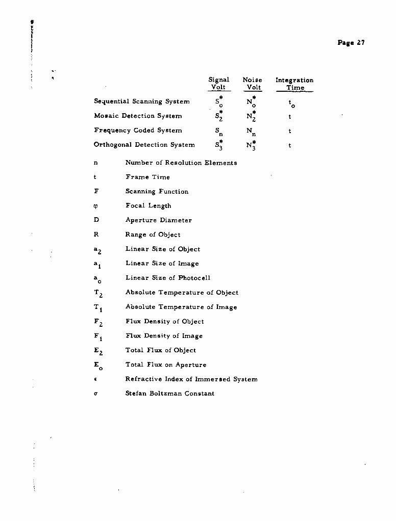
Signal Noise IntegrationVolt Volt Time
Sequential Scanning System S* N* to 0 o
Mosaic Detection System S2 N2 t
Frequency Coded System S N tn n
Orthogonal Detection System S* N3 t
n Number of Resolution Elements
t Frame Time
F Scanning Function
P• Focal Length
D Aperture Diameter
R Range of Object
a 2 Linear Size of Object
a i Linear Size of Image
a Linear Size of Photocell0
T2 Absolute Temperature of Object
*TI Absolute Temperature of Image
FZ Flux Density of Object
FI Flux Density of Image
E2 Total Flux of Object
E° Total Flux on Aperture
E Refractive Index of Immersed System
7r Stefan Boltzman Constant

I
Page 29
APPENDIX
THE DESIGN OF INFRARED IMAGING SYSTEMS
I. INTRODUCTION
The main body of this report illustrates the desirability of making the
sensitive area for the photocell as small as practical. It also analyzes the
signal-to-noise ratio of various imaging systems. It is desirable to utilize
as much integration time as possible to enhance signal-to-noise ratio. If a
mosaic system were designed where each resolution element of the image
has its own sensor, the full frame time could be used as integration time,
thus obtaining optimum signal-to-noise ratio. Such a system requires many
sensors and associated amplifiers to obtain high resolution and wide angle
views and is therefore, in many cases, impractical due to complexity, weight,
power-consumption and cost. It is therefore desirable to multiplex as many
resolution elements as feasible unto one sensor. This multiplexing can be
achieved by timesharing. However, timesharing reduces the integration time
available and thereby, the signal-to-noise ratio. Another method of multi-
plexing can be used by coding each resolution element with a different frequency.
This method is advantageous in cases where the response time of the cell is
fast, compared to the frame time available, in which case the frequency coded
system can approach the signal-to-noise ratio of the mosaic system.
The previous part restricts itself to theoretical analysis and does not
treat the practical design problems of dissection of two-dimensional images
or the methods of image reconstruction. This appendix will give some
practical design examples based on the previous analysis.
II. TWO-DIMENSIONAL IMAGE DISSECTION
Optical systems usually project two-dimensional images. Chopping
"reticles such as the one shown in Figure 5 are suitable to process one-
dimensional arrays of resolution elements. For example, the reticle
shown in Figure 5 contains a different chopping frequency on each radius.

Page 30
fa,-181216,0,4p~8 nd32 CYCLE.S/REM
Figure 5. Frequency Coded Raticle.

Page 31
There is no difference in signal output if the resolution element is at another
angular position as long as it is at the same radius. Note the reticle will cut
off approximately one-half of the radiant energy.
A. Mndulation of Carrier
A reticle, as shown in Figure 6, has a square wave amplitude modula-
tion superimposed on the carrier modulation of Figure 5. With this amplitude
modulation, a light spot in the image field will have a phase as well as a fre-
quency. If the phase relationship of the reticle is known, the angular position
of the light spot can be determined. The system requires the transmission of
an electrical signal indicating the position of the reticle. Since the signals
repeat in one revolution of the reticle, two such electrical signals, preferably
at right angle to each other for unambiguous determination of target position,
is required. Note the reticle cuts off approximately one-fourth of the radiation
intensity in the image. Furthermore, it is necessary to extract phase and fre-
quency of the signal. If there is more than one signal at one radius of the
reticle, the extraction of phase information becomes extremely difficult or
impossible. Only the stronger signal or the phase of the center of gravity of
the signals present may be obtained. Although this modulation of the carrier
signal can be somewhat improved by going from amplitude modulation shown
to a frequency modulation, the entire scheme is only applicable to tracking
systems where one must deal with one light-point only. For imaging systems
required for surveillance and cearch, the modulation of the carrier is not
suitable and other means must be found to dissect two-dimensional images.
B. Convert Two-Dimensional Image Into a One-Dimensional Array
Inability to process two-dimensional images directly, they must be
converted into one-dimensional linear arrays. There are three. basic ways
this can be accomplished, namely, optically, by timesharing, or by use of
multiple sensors. These three ways are discussed in greater detail in the
following paragraphs.

IPage 32
PHASE OF SIGNAL DETERMINES ANGULAR POSITION
fo4,6,12,16,20,24,28 and 32 CYCLES/REV
Figure 6. Frequency Coded Reticle(Amplitude Modulated).

Page 33
1. Optical Conversion
Using fibre optics, it is possible to rearrange a two-dimensi:onal
array of resolution elements into a linear one-dimensional array, which then
can be dissected with a reticle similar to the one shown in Figure 5.
In most cases of practical interest, there are too many resolution
elements to make it practical to process them all with one reticle, or with one
sensor. Therefore, this method, even if the difficulties of infrared fibre optics
are resolved, is only of academic interest.
2. Timesharing
Timesharing or sequential scanning results in a reduction on inte-
gration time available. Figure 7 shows a disc which can be used in conjunction
with the reticle of Figure 5 for this purpose. The disc of Figure 5 has one
revolution per frame time, while the reticle of Figure 5 rotates extremely
fast. Its speed of rotation is so fast that the highest frequency of the outer
ring is equal to one-half the response time of the sensor used. Note the inte-
gration time of this system is a/360 of the integration time of the previous
system. (See Figure 7, a in degrees. ) The angular position of the disc of
Figure 7 must be known to determine angular position of light spots. This
system is less complex but has a reduced sensitivity due to the reduced inte-
gration time. Furthermore, note that the frequency coded reticle is only
workable if the integration time available is large compared to the response
time of the sensor. (See Eq. 33.) This fact limits the usefulness of the time-
sharing metho.-' severely unless sensors with faster time constants become
available.
3. Use of Multiple Sensors
The two-dimensional image is dissected into horizontal strips
as shown in Figure 8. Each horizontal strip is processed by one sensing
cell. Using a reticle as shown in Figure 9, moving vertically, the linear
array of horizontal resolution elements is frequency coded. Note in this
system, one has frequency coding in the horizontal direction and an array-
like use of sensors in the vertical direction. A linearly moving belt reticle

Page 34
Figure 7. Timesharing Disc - I Revolution/Frame Time(To be Combined with Reticle of Figure 5).

Page 35
Figure 8. Image Area Divided into 8 Horizontal Strips.

!
Page 36
32 28 24. 20 16 124CYCLES/ FRAME
Figure 9. Reticle Belt Moving Vertical.

Page 37
has been chosen to achieve more even division of the image area into individual
resolution elements, as would be possible with a rotating circular reticle. All
the light of one horizontal strip has to be collected by a lens or an optical wave
guide unto a small sensor cell area. For images having many resolution
elements, this method using a combination of many frequencies and multiple
sensors is very suitable.
C. Comparison of Imaging Systems Discussed
Of the various possibilities to design imaging systems using frequency
coded reticles, the following conclusions can be drawn.
1. Modulation of the carrier is not suitable for imaging systems. It
is only useful for tracking systems.
2. A comparison table of two-dimensional imaging systems which use
frequency coding in one dimension follows.
System L 3
Ist dimension frequency coded frequency coded frequency coded
2nd dimension frequency coded timeshared multiple sensors
Remarks complex optics simple many amplifiers
Sensors required fast response for extremely fast availablemany resolution time constantelements necessary
Signal/noise good poor best
Most practical applications will use System 2 or 3 or a combination
thereof.

Page 38
D. Numerical Design Example
We choose, as a numerical example, a square image having
100 resolution elements on one side
10, 000 resolution elements total
1 second frame time
T = 1 millisecond time constant of sensor
The signal-to-noise ratio of the system is determined by the integration
time available.
1. Comparison System
The comparison system is a sequential scanning system examining
each resolution element in a time sequence. Such a system would therefore have
only 1/10, 000 of a second available for 1 resolution element. It would require
a sensor with a faster time constant. Since this sequential scanning system is
used only for purposes of comparison, this fact is disregarded. Its signal-to-
noise ratio is called So/No .
2. System Number 2
Vertical: Timesharing 100 resolution elements
Horizontal: Frequency coding n2 = 100 resolution elements
Integration time available t 2 = 1/100 second
According to Equation (33)
Tn. - must be small compared to 1
For this case:
n T= 100 1/1000 and
therefore this condition is not met and this system cannot be used.

I
Page 39
3. System Number 3
Vertical: Multiple sensor 100 resolution elements
Horizontal: Frequency coding n3 = 100 resolution elerments
Integration time available t 3 = I second
According to Equation (33)
n3 100 1 -/1000- I which is small compared to 1
therefore this system is feasible.
These evaluations show that the use of frequency coded reticles
combined with multiple sensors can result in considerable improvement of
signal-to-noise ratio. The system described requires 100 sensors with
associated amplifiers.
Note: To apply the same principles to imaging systems with 1
million resolution elements would require sensors with faster time constants
in order to be able to process, in the given frame time, more resolution
elements with the same sensing cell and arrive at a reasonable total number
of sensors.
E. Conclusions on Image Dissection Methods
The frequency coded reticle combined with multiple sensors offers
suitable means to design imaging systems with high signal-to-noise ratio.
For systems with many resolution elements, it is necessary to operate with
low frame rates and therefore, becomes desirable to use faster responding
sensing cells. Indium-arsenide sensors may be suitable for such applications.
Suitable impedance matching devices to the required amplifiers have to be
used with this low impedance sensor.

Page 38
D. Numerical Design Example
We choose, as a numerical example, a square image having
100 resolution elements on one side
10, 000 resolution elements total
1 second frame time
T = 1 millisecond time constant of sensor
The signal-to-noise ratio of the system is determined by the integration
time available.
I. Comparison System
The comparison system is a sequential scanning system examiningeach resolution element in a time sequence. Such a system would therefore have
only 1/10,000 of a second available for I resolution element. It would require
a sensor with a faster time constant. Since this sequential scanning system is
used only for purposes of comparison, this fact is disregarded. Its signal-to-
noise ratio is called So/No .
2. System Number 2
Vertical: Timesharing 100 resolution elements
Horizontal: Frequency coding n2 = 100 resolution elements
Integration time available t2 = 1/100 second
According to Equation (33)
n -L must be small compared to 12t Z
For this case:
1/1000n 100 1,ioo and
therefore this condition is not met and this system cannot be used.
I

I
Page 41
c. Light is transduced into an electrical square wave.
d. Electrical square wave is biased to have positive and negative
value s.
e. Electrical wave is used to modulate an illuminated electric
lamp so as to increase and decrease the existing illumination.
The illumination of the electric lamp, before it is modulated,
should be adjusted in order for the maximum, negative modulation amplitude to
produce approximately zero light output.
. For example, where the frequencies of modulation are 1, 2, 4,
6, 8, and 10 cycles per frame time, Figure 10 shows the modulated light output.
Using a reticle exactly like the dissecting reticle and synchronized with the
dissecting reticle, the light from the electric lamp diffused into a linear array
behind this reticle will show in the corresponding resolution element where it
was originally in the image. The mathematical operation performed by this
filtering or image reconstruction reticle is,
"t t'o tZVJun Rf-V
Ai A dt
t'OIIf

Page 42
where
t frame time0
n number of resolution elements
f ch6pping frequency
u even integer
v odd integer
This operation is illustrated in Figure 10.
It will be difficult to device a more compact and efficient filter
than this optical correlation through a second reticle described.
IV. SYSTEM DESCRIPTION
An example of such a system using moving belt reticles is illustrated in
Figure 11. This system uses multiple sensors and multiple glow lamps in the
vertical direction and multiple frequencies in the horizontal direction. The
reconstructed visible image can be viewed directly or further processed using
standard television techniques.
V. RECOMMENDATION
It is recommended that tests on the described system be conducted to
evaluate obtainable signal-to-noise ratios experimentally. Furthermore,
the development of faster time constant sensors and their practical appli-
cation is necessary in order to extend this technique to high resolution systems.

Page 43
00S4,
"~ g a
1
rF 00LF1 ',
'a.
i0
asa
.0 -C

Page 44
fill

I0 IC~~~ Z 04 so " '0'Z~I
* ~ .0 ~ 4 0~ 41 41f go41
-az ~~~~ ~ 4 >*A:e .1v--.
0 0
7j 0 ' -
Q . .,fu .00 l
9F1 g149 1*-. 0 0 0 .a O u
A" ý.u -oE-r n o 45u 0
0,4 A1 0 ,
~~l ~ ~~ J.r

.0 i
~ 'U0
u u
•l '~ **. ,-I.
u- •l...-'•,•t..
u u
12