ad-a259 773 u h uu technical report · technical report growth and doping ... p.i. theodore d....
TRANSCRIPT

AD-A259 773 0U H UU Semniannual. Technical Report
Growth and Doping of AM.Gal_=N Films by Electron CyclotronResonance Assisted Molecular Beam Epitaxy
DTICONR Grant No. N00014-92-J-1436 ELECTE
(May 1, 1992 - April 30, 1993) EL2193
S FEB 2 1993DCP.I. Theodore D. Moustakas
Department of Electrical,Computer, and Systems Engineering
Boston Univeristy NBoston, MA 02215617-353-5431
Approved for Public Release; Distribution Unlimited
October 30, 1992
"93-01874
4liMnn -
1 30 ct. 192 Seiannual 01 May 1992 30 Aor 19931S. IWCNGM m-UMB[R5
Growth and Doping of ALL Ga I Films by Electron CcornR&T.. 4145329---01
Re~onance Assisted Molecular Beam Epit~axy S.0: 1114SSAGO: N66017
j. ALIT 4OR(S) GAGE: 3A817
Moustakas, Theodore D.
7.p~piCA~iNc ORGA.412A71CMN AMEIS/ ANG AZCRE53SiE5; 3. PE.0MCRMING CgG1N' ýL.Ch
Boston UniversityCollege W-f.. Engineering -NO0014-92-J-i43644 Cummington St.Boston, MA 02215
r. SCNSCRINGIMCNITGAIN4~ AGZNCYý NAME15) A.40 A0CRE5-34!5; IQ ;0 iIG
-S 7 ~~AGENC! aiECR NQ'E;Department of the NavyOffice of the Chief of Naval Research800 North Quincy St, Code 1511:KIJ
I Arlington, VA 22 217 -5000
11. SUPPL.EMLNTARY NOTE5
Ilai. CIS7RIBUTION , AVAILAZlL:TY -T7--,--T" C
Approved for Public Release; Distribution Unlimited N00179
13. APSTRACT (Ajiomvrn2Qoo-orc;)Growth and doping of CaN by MR assisted MBE is reported.We report on the role of the CaN-buffer and AlN-buffer, and their. :comb ina tion on th~two dimensional nucleation rate and lateral growth rate. Conditions for quasi layerby layer growth were identified. XRfl was used to study secondary phase, the .direction and quality of orientational ordering in and out of the substrate, andhomogeneous and inhomogeneous strain. Relatively high mobility autodoped films wer-produced and their traasport mechanism was investigated. Intrinsic GaN-f ilms were produced and were doped n- and p-type with Si and Mg respectively,without requiring annealing for dopant activation. RIE processing of CaN wasdeveloped and metal contacts were investigated. A direct correlation between themetal work function and barrier height was also found.
"1. 1IS. ,,WBER C; ?-"-"89~Gallium Nitride, Aluminum Gallium Nitride, .Molecular Beim . 6 RCC0
,Epitaxy, Electron Cyclotron Resonance source, n-dop~ing, . 6PIiCt
1 .SCRT LASC ATION 18. SECURITY CLASSIfICATION 19. SECURITY CLASSIFICATION 2.LIMITATIOA , STRCOF REPORTAG Of ABSTRACT
'CLA'S UNCLAS JntCLAS-----
Table of Contents
1. Results during the first six months of the current funding year ....................... 21.1 Heteroepitaxial Growth of GaN by ECR-assisted MBE ........................ 21.2 Atom ic Structures Studies .................................................... 21.3 Growth of High Mobility GaN Films .......................................... 31.4 n- and p-doping of GaN film s ................................................. 31.5 Ohmic Contacts / Processing of GaN ......................................... 3
R eferences ............................................................................. 4
Appendix A: "Growth of GaN by ECR-Assisted MBE"Appendix B: "Heteropitaxy, Polymorphism and Faulting in GaN Thin Films on Silicon andSapphire Substrates"Appendix C: "Electron Transport Mechanism in Gallium Nitride"Appendix D: "Metal Contacts to Gallium Nitride"
Aeo•,mi'p•
awl* USM
TIC QtTALfYf ITSPECM 3 1Avtioablity Codes1; 'Avnil axd/or-
Dist Special
1+- ! I

1 Summary of results during the first six months of
the current funding period
During the first funding year the work is focused on the heteropitaxdal growth and dopingof GaN films by the method of Electron Cyclotron Resonance microwave plasma assistedMolecular Beam Epitaxy. A brief description of specific a•ccomplishements during the first
six months of the current grant are listed below-
1.1 Heteroepitaxial growth of GaN by ECH-assisted MBE.
The heteroepitaxial growth of GaN on a '-arlety of substrates 'Si(100), Si(1l1), sapphire ( c,
a, R-planes)] by the ECR-MBE method was investigated, using a two step growth process
for GaN which specifically separates the nucleation and -rowth phases. Since the nucleation
rate depends exponentially on 11T it is dear that the nucleation dominated reime occurs
at low temperatures. Thus, we developed a low temperature buffer which covers uniformly
the substrate due to the large nucleation rate. The growth of the rest of the film occurs
at relatively higher temperatures and should be close to homoepitaxy. Under equilibrium
conditions, homoepitaxy should proceed in the layer-by-layer mode without the formation
of nuclei. However, due to imperfections of the buffer layer, nuclei may form at the suface
edges and steps at small contact angles. Recently we were able to form GaN film with an
extermely low two-dimensional nucleation rate (-- 20nuclei/mI2 - h) and lateral growth rate
100 times the vertical growth rate. Thus, under these conditions, the growth is quasi layer-
by-layer. (1,2)
Besides the GaN-buffer, we have recently developed an AIN buffer not by a deposition
process but by nitridation of tL- sapphire substrate. We found that the conversion of Al 203surface to AIN requires exposing the substrate, held at 8500, to an ECR nitrogen plasma
for approximately 10-15 min. This AIN layer appears to be atomically smooth based on the
elongated RHEED pattern(2,3). We found that the GaN-buffer, which is usually grown at
lower temperatures (approximately 4000 C), is atomically smooth, when grown on the top
of this AIN buffer. Furthermore, GaN films grown on the combination of AlN-GaN buffers
were found to have the best surface morphology with lateral growth rate much higher than
the vertical growth rate. Details of these results are presented in Appendix A.
1.2 Atomic Structure Studies.
The structure of GaN films grown on a variety of substrates [Si(100), Si(111), sapphire (c,
a, R-planes)] was studied with four-circle X-ray diffractometry. These studies allowed us
to determine the presence of secondary phases, the direction and quality of orientational
ordering in and out of the substrate plane and the homogeneous and inhomogeneous strains
in the film. Our studies show that wurtzite and zincblende GaN polymorphs often coe.-st
L- fdxns which grow with their close-packed stacking planes parallel to the substrate. The
evidence suggests that the zincblende phase may nucleate at stacking faults (4). Details on
these studies are described in Appendix B.
2

1.3 Growth of High mobility GaN films and transport mecha-nism in GaN.
We have been able to grow auto-doped Ga¶ films systematically with carrier concentrationsfrom 1019 to 2 x 101c-m-A. Simultaneously, the electron mobility increased from about 20cM2//V-sec to 210 cm 2/V-sec. These results are illustrated in Fig. 1. It is interesting to notethat this curve extrapolates to a mobility of 600 cm-/'V-sec reported for GaN films grown'by the MOCVD method (5). Based on the temperature dependent transport measurements.a picture of simultaneous transport in the conduction band and the autodoping centers hasemerged. When the concentration of the autodoping centers becomes less than the con-centration of the deep defects, the material becomes fully compensated, leading to hoppingconduction in the deep compensating defects, accounting for the low electron mobility inthese films(6). Details on these studies are p -- ented in Appendix C.
1.4 n- and p-doping of GaN films.
Plasma modes with high nitrogen plasma density were identified which allow the growth ofsemi-insulating GaN films.
Such GaN films were doped n-type with Si, a common dopant in MBE growt'. Silicon wasincorporated as a donor with a net carrier concentration of ND - JVA = 2 x 1018cm- 3.
GaN films produced under the growth conditions which lead to intrinsic films were dopedp-type by the incorporation of Mg. Carrier concentrations up to 2 x 10¹⁹ were obtainedwithout requiring an additional annealing step as reported previously (5,7). These studiesare still in progress and will continue during the second half of the funding year.
1.5 Ohmic Contacts / Processing of GaN.Rep.Aive Ion Etching (RIE) techniques have been developed to process GaN films. Etchingwas carried out in Freon 12, at 140A/min and selectivity 3:1 for GaN/photoresist (8).
The rectification properties of various metal contacts to GaN were investigated. A directcorrelation between the metal work functions and barrier height to GaN was found, a resultattributed to the ionic character of GaN. Thus, ohmic contacts to both n- and p-type GaNcan be made by choosing metals with the appropriate work functions (Al for n-type and Aufor p-type) (9). Details on these studies can be found in Appendix D.
3

S it 0 ; ! . 1, 1 rI I it I; II . I- I I I III I l III M i I I I i 1 1 1 I II T
;i l 1 T
T 7 . ý I ! T il0!1
1 1 : i I I 1
T; T 7. 7. 1 1 11 11i II I I I I
!;I ýIt jlý ý,I ;: i I i! ll$ i l I I 7 1 7,1 1 F.1 0
a) L-4r

References:
1. "Epitaidal growth and characterization of zinc-blende gallium nitride on (001) silicon,"T. Lei, T.D. Moustakas, R.J. Graham, Y. He, and S.J. Berkowitz, J. Appl. Phys. 71.4933 (1992).
2. "Growth of GaN by ECR-Assisted MBE," T.D. Moustakas, T. Lei, and R.J. Moinar.Physica B: Condensed Matter (Accepted for Publication).
3. "A Comparative Study of GaN Films Grown on Different Faces of Sapphire by ECR-Assisted MBE," T.D. Moustakas. R.J. Molnar, T. Lei, G. Menon, and C.R. Eddy Jr.,Mat. Res. Soc. Symp. Proc. Vol. 242, 427 (1992).
4. "Heteroepitaxy, Polymorphism, and Faulting in GaiN Thin Films on Silicon and Sap-phire Substrates," T. Lei, K.F. Ludwig Jr, and T.D. Moustakas, J. Appl. Phys. (Sub-mitted for Publication).
5. "Conductivity Control of AIGaN, Fabrication of AMGaN/GaN Multiheterostructaresand Their Application to UV/Biie Light Emitting Devices," I. Akasaki and H. Amano,Mat. Res. Soc. Symp. Proc. Vol. 242, 383 (1992).
6. "Electron Transport Mechanism in Gallium Nitride," R.J. Molnar, T. Lei, and T.D.Moustakas, Appl. Phys. Lett. (Jan. 1993).
7. "Thermal Annealing Effects on P-Type Mg-Doped GaN films," S. Nakamura, T. Mukai,M. Senoh, and N. Iwasa, Jpn. J. Appl. Phys. Vol. 31, L139 (1992).
8. "Ohmic Contacts and Schottky Barriers on Gallium Nitride," 3. Foresi, M.S. Thesis(Boston University, 1992).
9. "Metal Contacts to Gallium Nitride," J. Foresi and T.D. Moustakas, Appl. Phys. Lett.(submitted for publication).
4

Appendix A:
Growth of GaN by ECR-Assisted MBE

accepted for publication:Physica B: Condensed Matter
Growth of GaN by ECR-Assisted MBE
T. D. Moustakas, T. Lei, and R..J. Molnar
Molecular Beam Epitaxy Laboratory
Department of Electrical, Computer and Systems Engineering
Boston University, Boston, MA 02215
AbstractHigh quality GaN films have been grown on a variety of substrates
by Electron Cyclotron Resonance microwave plasma-assisted Molecu-
lar Beam Epitaxy (ECR-MBE). The films were grown in two steps.First, a GaN-buffer was grown at low temperature and then the rest ofthe film was grown at higher temperatures. We found that this method
of growth leads to a relatively small two-dimensional nucleation rate (-
20 nuclei/pm 2 .1h) and high lateral growth rate (100 times faster than
the vertical growth rate). This type of quasi-layer-by-layer growth re-sults in smooth surface morphology to within 100At. Growth on Si(100)leads to single crystalline GaN films having the zinc-blende structure.
Growth on Si(111) leads to GaN films having the wurtzitic structurewith large concentration of stacking faults. The crystallographic orien-tation and the surface morphology of GaN films on sapphire depends
on the orientation of sapphire. To this date, the best films were grown
on the basal plane of sapphire.
1 Introduction
The family of refractory nitrides (InN, GaN, and AIN), their solid solutions and het-
erojunctions are one of the most promising families of electronic materials. All threeare direct bandgap semiconductors with their energy gaps covering the region from1.95eV (InN)and 3.4eV (GaN) to 6.28eV (AIN). Thus, the growth of high quality
crystals and successful doping of these materials should lead to applications in op-toelectronic devices from the visible to the ultraviolet part of the electromagneticspectrum, as well as in devices for high power and high temperature electronics [1-2].
CaN, in particular, was predicted to have a high electron drift velocity, so it shouldalso be suitable for high frequency and microwave devices [3].
GaN films have been grown by many growth techniques, including Chemical Vapor
Deposition [4-7], Metal-Organic Chemical Vapor Deposition [8-15], Molecular Beam

Epitaxy (16-25], and a number of plasma-assisted processes (26-30]. A variety of sub-strates such as silicon, spinel, silicon carbide, and various crystallographic orientationsof sapphire have been used in these studies. Most of the films grown are wurtzitic
(a-GaN), and have n-type conductivity with high carrier concentration [311, which is
believed to result from nitrogen vacancies 131-32) or oxygen impurity incorporation
[33]. P-type conductivity has been reported recently on Mg-doped GaN films [34-35].Zincblende GaN(I3-GaN), which is the thermodynamically metastable phase of
GaN, is hoped to be more amenable to doping than the wurtzitic GaN, since all of
the III-V compounds that can be efficiently doped n-type or p-type are cubic [2]. 0-GaN has been epitaxially stabilized on f3-SiC and MgO(100) substrate [18-19], which
are closely lattice-matched to fl-GaN, and on GaAs [36-37] and Si substrate [21-25]which have significant mismatch to 8-GaN.
In this paper, we review the growth of GaN films by the Electron CyclotronResonance microwave plasma-assisted Molecular Beam Epitaxy. Particular emphasisis placed on the growth of this material in two temperature steps which was developed
recentlv in our laboratory [21-25,3S]. Films were grown on Si(100), Si(111), andvarious faces of sapphire.
2 Experimental Methods
The deposition system used in this study is schematically illustrated in Fig. 1. TwoECR sources were used. The first (Astex 8" model 1000) was used for the growth of
GaN on Si(100) and Si(l11). The second (Astex compact model) was used for thegrowth of GaN on sapphire. The pressure in the overall system was 10-11 Torr. AReflection High Energy Electron Diffraction (RHEED) setup is an integral part ofthe apparatus. A conventional Knudsen effusion cell was used to evaporate gallium.Atomic and ionic nitrogen were produceed by passing molecular nitrogen through theECR source. Part of the molecular nitrogen was also introduced downstream of theECR source. Typically, 10% of the molecular nitrogen gas is converted into atomicnitrogen. Due to this high decomposition rate, a source pressure of about 10-4 Torr issufficient for the growth of stoichiometric films. The magnetic field configuration forthe 8" source under optimized conditions for the growth of GaN films is illustratedin Fig. 2. The on-axis ECR condition (H = 835 Gauss) is about 40 cm above thesubstrate. The compact ECR source fits inside an effusion cell and thus the distancefrom the front of the source to the substrate is only 12 cm.
The structure and microstructure of the films were studied by Reflection HighEnergy Electron Diffraction (RHEED), X-ray diffraction and Scanning Electron Mi-croscopy (SEM). X-ray diffraction studies were performed using a diffractometer with
2

four-circle geometry. This allows us to perform O-scans at a reflection peak (hkl),corresponding to planes not parallel to the substrate to probe in-plane ordering. Ad-ditionally, standard MO2O scans -were performed to probe the ordering.normal to thesubstrate.
Si(001) and Si(111) substrates (n-type, p-type or undoped) were used in thesestudies. They were ultrasonically degreased in solvents and etched in buffered HF toremove the oxides, prior to their introduction into the MBE unit. In the preparationchamber, the substrates were outgassed for 15 minutes at 850°C.
The sapphire substrates were subjected to the following cleaning steps prior tothe growth of the CaN films. They were sequentially cleaned in ultrasonic baths oftrichloroethylene, acetone, and isopropanol for removal of hydrocarbon residues fromthe surface, etched in H3PO4 : H2S0 4 (1:3) for the removal of surface contaminantsand mechanical damage due to polishing and finally rinsed in de-ionized water. Afterthese steps, the substrates were blown dry with nitrogen, mounted on a molybde-num block and transferred to the introduction chamber of the MBE system. In thepreparation chamber, the substrates were heated to 8500C for approximately halfan hour and then transferred to the growth chamber where they were subjected tobombardment by nitrogen plasma for approximately half an hour at 7000C.
3 Experimental Results
_3.1. Growth on Si(100).
Following cleaning, the Si substrate was examined by studying its RHEED patternin the growth chamber at 4000C. Fig. 3 shows typical RHEED patterns of the Sisubstrate with the electron beam incident along (100] and (110] directions. Theseresults clearly indicate that the Si(001) surface is unreconstructed (i.e. 1 x 1). Wefind that such an unreconstructed Si(001) surface is required to epitaxially grow asingle crystalline GaN-buffer. Outgassing of the Si substrate at lower temperatures,for example 6000C, leads to an irregular pattern with few diffraction spots, whichwe were unable to index with any reconstruction pattern. A CaN-buffer grown onsuch a surface would generally be polycrystalline with the wurtzitic structure. It isconceivable that epitaxy of GaN should take place on a well ordered unreconstrutedsurface, but not on an irregular disordered surface.
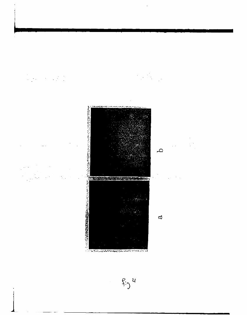
After the substrate preparation and characterization, a GaN-buffer layer of about300A to 900A thich was deposited at a temperature of 400"C for 10 to 30 minutes,Fig. 4 shows the RHEED pi. .rns at two azimuthal incidence of the electron beamfor the CaN buffer layer. The diffraction spots are relatively broad, signifying that
3

the thin buffer laver is very defective. This is expected due to the large lattice
mismatch between the film and the substrate. However, the symmetry of the patternsindicates that the buffer layer has the zincblende structure with the 1001] direction
perpendicular to the substiate.Following the deposition and characterization of the GaN-buffer the substrate was
heated to a higher temperature, typically 600°C, and a GaN film of about 1 jm thickwas grown at a growth rate about 2000A/h. Shown in Fig. 5 (a) and (b) are typicalRHEED patterns of a GaN film about 1 am thick grown on a p-type substrate for[100] and [110] azimuthal incidence of the electron beam. The results are similar whenthe growth takes place on undoped substrates. These results clearly indicate that the
GaN film has the zincblende structure, with its (001) crystallographic planes parallelto the substate surface. The diffraction spots of this pattern are significantly sharperand elongated, which suggests that the final GaN film has a better crystalline qualityand a smoother surface morphology than the GaN-buffer.
The RHEED pattern of a GaN film grown on a p-type substrate under slightlylower nitrogen pressure is shown in Fig. 6. The streak-like pattern is characteristicof two dimensional scattering, indicating that the GaN film is close to atomicallysmooth. Such elongated RHEED patterns were frequently observed when the growthtook place on n-type substrates. This may suggest that GaN wets to the n-typesubstrate better than the p-type substrate. Morimoto and co-workers reported thatin vapor phase growth, GaN adhered to n-tYpe silicon, but not to p-type siliconsubstrates.
In a few cases, the Si substrate was first bombarded with nitrogen plasma priorto the formation of the GaN buffer. The lack of a RHEED pattern indicates thateither an amorphous SiN film was formed on the substrate or that the surface wasdisordered. The GaN buffer grown on nitrogen plasma bombarded substrates werefound to be polycrystalline having the wurtzitic structure with the (0002) preferred
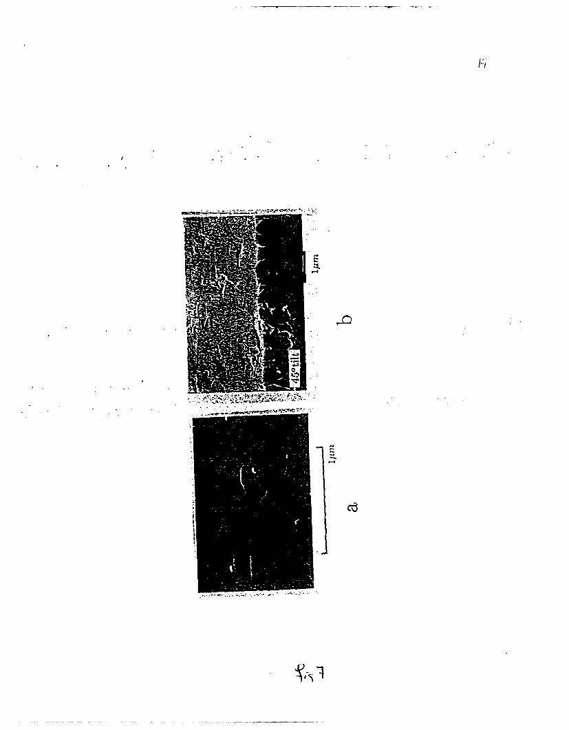
orientation.Shown in Fig. 7 are the surface morphology and the cross-sectional view of a
fl-CaN film on a p-type silicon substrate studied by SEM. It can be seen that the filmhas a relatively flat surface, roughened with many well-oriented rectangular shaped'tiles', which reflect the symmetry of the P3-GaN (001) surface. The cross-sectionalview shows no evidence of columnar morphology, which is another indication that thefilm is single crystalline.
Detailed electron microscopy studies (231 have shown that the tiles in Fig. 7 areoriented along the [110] and [110] directions. This presumably arises because the GaNsurfaces corresponding to those directions are more closely packed than the [100] and[010] surfaces and therefore have lower surface energy.
4

Shown in Fig. 8 (a) is the morphology of the GaN film, whose RHEED pattern%.as discussed in Fig. 6. The surface morphology of a film on an n-type substrateis showa in Fig. 8 (b). Both of these surfaces are smooth with steps approximately
10DAt'hick, which resulted from a layer-by-layer growth [231. TY- se results suggest
that additional optizimation of the growth process could lead to atomically smooth
surfaces.
From the data of Fig. 8, we can calculate the two-dimensional nucleation rateand the lateral growth rate. Let J be the nucleation rate, s be the average area of the
plateau, h be the height of the plateau, and t be the time for the plateau to grow,which is limited by nucleation. Then, we have
V,
-vt (Js)()
and
h vt =V (2)(Js)
where v1. and vn, are the lateral and vertical growth. rates respectively. From thedata of Fig. 8, we have Vs 1upm and h • 100ioA. It we use the known verticalgrowth rate v,, = 2000 A/h, then from (1) and (2) we obtain v1 = 100V,, and J ý_ 20
nuclei/(pm'-h).These data indicate that this two-step method of film growth leads to quasi-layer-
by-layer growth with very small two-dimensional nucleation rate and high lateral
growth rate.The structure of the films was confirmed by Convergent Beam Electron Diffraction
(CBED) and Selected Area Diffraction (SAD). These studies were published elsewhere
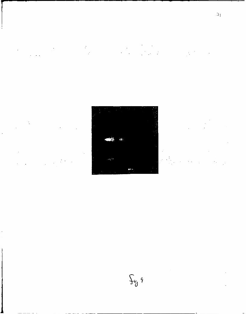
[23]. In this paper, we focus on the X-ray diffraction studies of the films.The X-ray diffraction in Fig. 9 shows a strong peak at 20 = 40.1 degrees, whose
d-spacing is 2.25 A, which is due to (002) reflection from fl-GaN. Hence, the latticeconstant to /3-CaN was found to be .4.50 A, in good agreement with the electrondiffraction data [23]. A small peak was also observed at 20 = 34.6, which is due tothe d-spacing of (111) fl-GaN or (0002) a-GaN. This suggests that the (aN film hassome misoriented domains. These domains may have developed in the early stagesof the buffer layer deposition as revealed by TEM imaging [39]. Similar structuralfaults have also been observed in the interface betweer-. CaN epitaxy on GaAs(100)[371. We have also observed these misoriented domains in almost all of our samples.
The consistent appearance of the misoriented domains in CaN-Si and CaN-GaAs het-eroepitaxy is very likely to be related to the large lattice mismatch between the GaNand the substrate. Because of the large lattice mismatch, the interface of GaN and thesubstrate is under significant strain; therefore, it might be favorable for the system
5

to introduce dislocations or misorientations of GaN to reduce the interfacial energies.In zincblende or wurtzitic structures, the [111] or [0002] planes are the most closely
packed, and hence have the lowest surface energies. Therefore, the introduction of
[111] or [0002] oriented (aN would lower the surface energy at the CaN-vapor inter-face, and would not necessarily increase the energy for the CaN-substrate interface,since it was strained significantly. However, the [111] or [0002] oriented CaN domainswould grow slower than the [001] oriented CaN grains stabilized by introduction ofdislocations. As a result, they were buried in the interface region as the film grew.
The X-ray rocking curve of the [002] peak of a CaN film 4 pm thick was found tohave a Full Width at Half Maximum (FWHM) of approximately 60 minutes, whichmeasures the orientation spread perpendicular to the substrate. This is significantlynarrower than that of CaN on GaAs [37], but much broader than that of 68-GaN onMgO substrates [19] and a-GaN on [0001] sapphire substrates as discussed later.
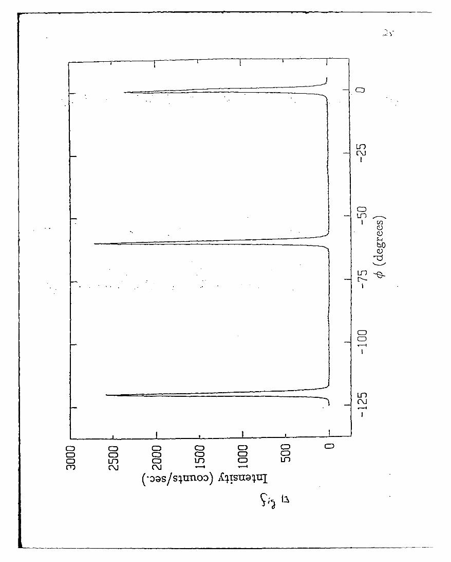
The ý-scan for the zincblende GaN was performed at the [111) reflection, andis shown in Fig. 10. The data clearly show that the peak repeats itself every 90degrees, consistent with the cubic symmetry of this material. The FWHM of thesepeaks, which measures the in-plane orientation spread, was found to be 2.5 degrees.
3.2 Growth on Si(111)
Growth on Si(11) followed the same steps as dlescribed previously in the growth on"Si(001). Fig. 11 shows the RHEED pattern for a GaN film on Si(1!1). The dataindicate that the -film has the wurtzitic structure with the [0001] planes parallel tothe substrate. The sharpness of the diffraction spots indicate good crystalline qualityof the film.
Fig. 12 shows a 0-20 scan for a GaN film on Si(I11). The single peak at 34.6degrees corresponds to [0002] reflection of the wurtzitic CaN; thus, the lattice constantin the c-direction is 5.18 A
The O-scan for the wurtzitic GaN shown in Fig. 1.3 was performed at the [1102]reflection. Clearly, this peak repeats every 60 degrees, consistent with the 3 mmsymmetry of the rotation axis. The FWHM is found to be 1.9 degrees, while theFWHM of the 0-20 rocking curve at the [0002] peak is found to be 0.9 degrees.
The XRD data of Fig. 12 and Fig. 13 appear to indicate that the a-CaN film onSi(1 11) is a single crystal. However, any stacking faults along the growth direction ofthe CaN film on Si(111) can not be easily detected in the normal 0-20 scans [40]. Suchstacking faults are very common defects in materials with the FCC or HOP structuresgrowing along the [111] and [00021 directions [40]. Such stacking faults, if they exist inthe wurtzitic GaN films on Si(111), should give rise to a certain amount of cubic CaNcomponent with the [111] planes parallel to the substrate. To explore this possibility,
6

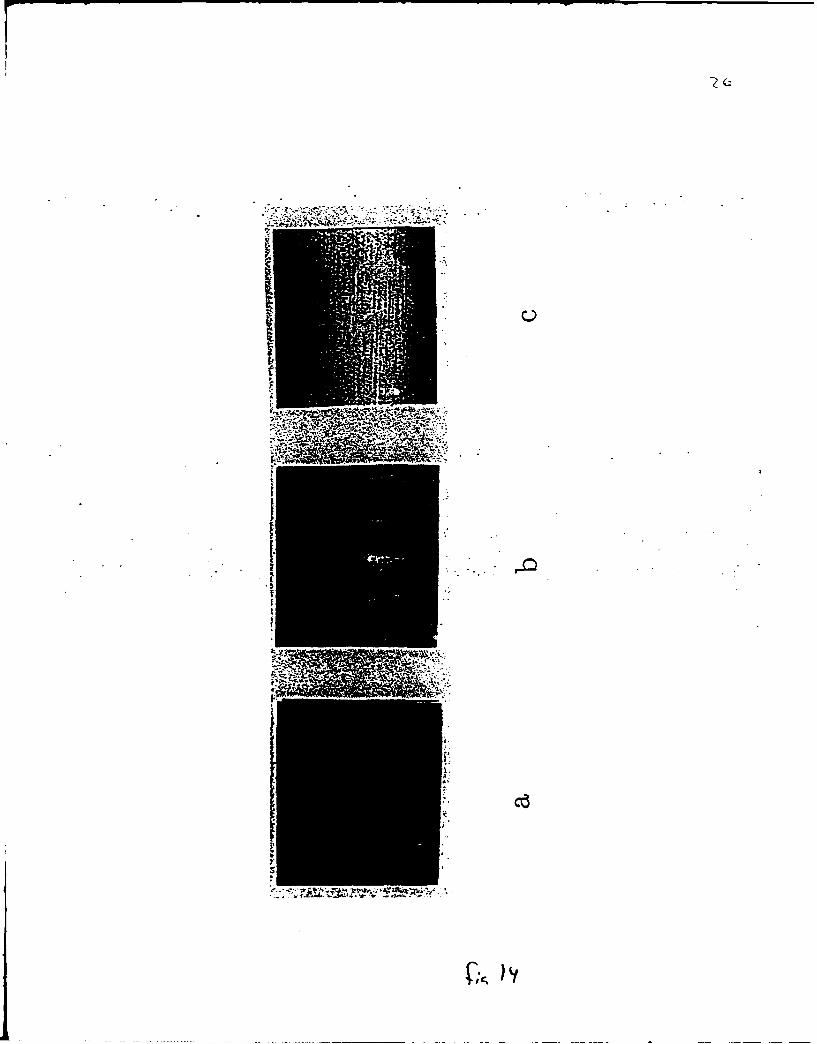
we rotated the sample in such a way that the X-ray diffraction corresponds to the(0021 reflection of the zincblende structure, and indeed a peak was detected at 20 =40 degrees. This is shown in a 0-20 scan around this peak (see Fig. 14).
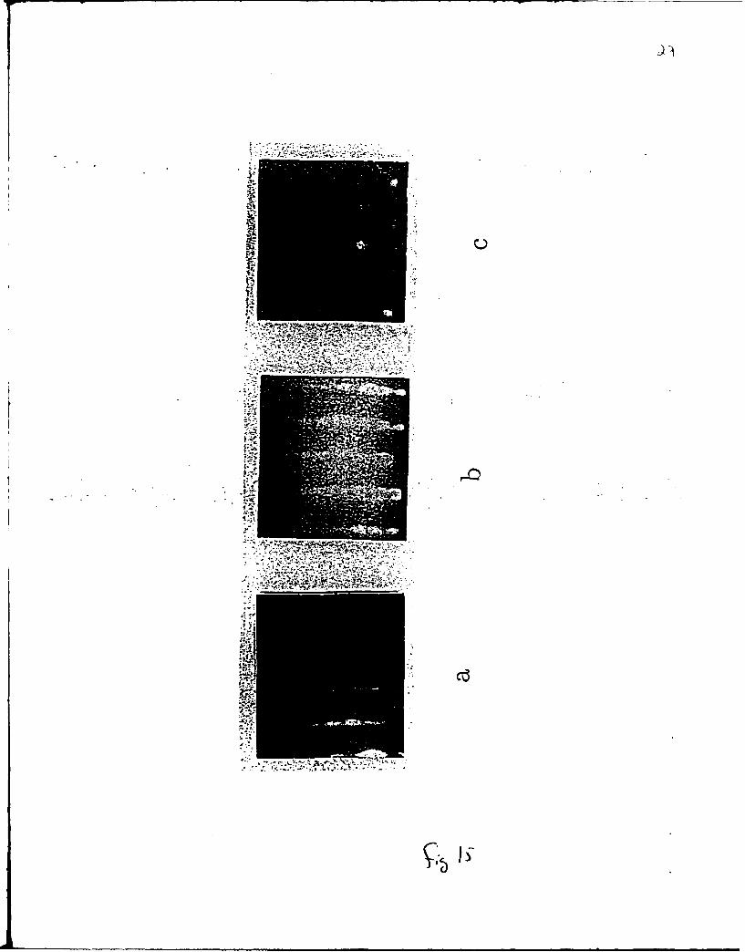
To obtain 'A -stronger -reflection, a-scans on these cubic domains were performedat [iIf] *peak, which is shown in Fig. 15. These data reveal a repetition every 60degrees. Since the [111] axis in the zincblende structure is only a 3-fold rotational axis,the ý-scan should show a repetition every 120 degrees instead of every 60 degrees.Therefore differing by 60 degrees in 0. This can be accounted for if there are twokinds of stacking sequences, namely ABC... and CBA... sequence. The fact the peakat 0 = 60 degrees is of comparable intensity to the other two peaks suggests that thetwo types of stacking sequences occur with an equal probability, as is expected.
The existence of the cubic GaN domains in the wurtzite structures implies theexistence of high concentration of stacking faults. This could be due to the fact thatthe cohesive energies of wurtzite and zincblende GaN are comparable, so that theformation energy of a stacking fault is negligible. If this is true, then all of the [0002]oriented GaN films have a considerable amount of stacking faults. This is currently.being investigated by XRD studies of GaN on [11201 and [0001] sapphire substrates.However, one should not rule out that the high concentration of stacking faults inGaN on Si(l11) is related to strain resulting from the large lattice mismatch betweenGaN and Si, which could lead to reduction of the formation energy of stacking faultsdue to structural deformation.
3.3 Growth on Sapphire Substrate
GaN films were also grown on the c-plane [00011, a-plane 11120] and r-plane [11021 ofsapphire. Fig. 16 shows RHEED patterns of the three types of substrates after theexposure to the nitrogen plasma. The data indicate that the surface of the substrateswere nitrided and from the diffraction patterns, the lattice constant of the AIN wasestimated to be a = 3.1 A1. Furthermore, the streakiness of the diffraction patterns,in particular those of the c-plane and a-plane sapphire substrates, suggests that theAIN layers are atomically smooth.
Fig. 17 shows RHEED patterns of the GaN-buffer on the three types of sub-strates. The data indicate that the GaN-buffer is single crystalline on all three typesof substrates. The GaN films grown on the c-plane and a-plane sapphire substrateshave their c-plane [0001] parallel to the substrates, while the GaN films grown on ther-plane of sapphire have their a-plane [1120] parallel to the substrate. The streaki-ness of the diffraction patterns of the GaN-buffers on the c-plane and a-plane sapphiresubstrates suggests that the GaN-buffer on these substrates are atomically smooth.
Fig. 18 shows RHEED patterns of the GaN films at the end of each run. These
7

reveal the same epitaxial relationship between GaN films and the substrates as the
corresponding GaN-buffers discussed in Fig. 17. Also, the films on the c-plane a.da-plane sapphire substr.ates are atomically smooth.
Fig. 19 shows the surface morphology of GaN films grown on the three types of
substrates. The films on the a-plane have the smoothest surface morphology. The
surface morphology of GaN films on the c-plane consists of interconnected tiles several
thousand angstroms in size. The GaN films grown on the r-plane sapphire were found
to have the roughest surface morphology. The pyramidal surface morphology is likelyto be related to the fact that the a-plane of GaN is bounded by two prism planesunder equilibrium growth conditions.
Fig. 20 shows the 0-20 XRD and the 0-rocking curve at the main reflection peakof the GaN films grown on the three types of substrates. The main reflection peakfor the GaN films grown on the c-plane and a-plane sapphire occurs at 20 = 34.6degrees, corresponding to the [0002) reflection. This confirms that films were grownwith their c-planes parallel to the substrate. The main diffraction peak of the GaNfilm on the r-plane of sapphire occurs at 20 = 57.S degrees corresponding to the GaN[11201 reflection. This confirm the RHEED study that the a-plane of the GaN filmis parallel to the substrate. The rocking curve of the GaN film on the c-plane of
sapphire has the smallest width (FWHM = 10 min.), indicating that the crystalline
quality of these films to be the best. Such films were also found to have the highestelectron mobility (I >.-200 cm 2/V.s) among films grown by MBE processes.
The epitaxial relationship of the GaN films to the c-plane of sapphire is to be
"expected. However, the epitaxial relationship of the GaN films on the a-plane andr-plane of sapphire is not obvious. This epitaxial relationship can be accounted for
as follows: The a-plane sapphire has a rectangular unit cell with dimensions 12.97 Ax 8.23 A, two of which can accomodate a number of unit cells of GaN basal planesas illustratedin Fig. 21 (a). This results in 1.6% lattice mismatch along [0001] ofsapphire and 0.6% along [1100] axis of the sapphire substrate. The r-plane of sapphiresubstrate has a unit cell with dimensions 4.75 A x 15.34 A, which accomodates threeunit cells of the a-plane of GaN as illustrated in Fig. 21 (b). This results in 16%lattice mismatch along the [1120] of sapphire and 1.3% along the [1101] of sapphire.
4 Conclusion
In conclusion, a two step growth process has been developed for the heteroepitaxial
growth of GaN films. This method was found to lead to films with smooth surfacemorphology, which we interpreted as resulting from a quasi-layer-by-layer growth.
Using this process GaN films were grown on a variety of substrates by ECR assisted
8

MBE.
GaN films were successfully grown on Si(001) and (111) substrates, using this two-step process. The films on Si(001) are single-crystalline, and epitaxially stabilized inthe zincblende structure, while those on Si(111) have the wurtzite structure. AlthoughRHEED suggest that the wurtzitic GaN on Si(111) is single-crystalline, considerableamount of cubic phase was detected by XRD studies, and was attributed to largerconcentration of stacking faults along the growth direction.
GaN films were also grown on the c-plane, a-plane, and r-plane sapphire. Thegrowth process involves the conversion of the sapphire surface into AIN by plasmanitridation. The XRD studies indicate that GaN films on the c-plane sapphire havethe best crystalline quality.
Acknowledgements
We are grateful to Prof. Karl Ludwig for stimulating discussions and help withXRD studies. This work was supported by the Office of Naval Research (Grant No.N00014-92-J-1436).
References
[1] R. F. Davis, Proceedings of the IEEE., V. 79, No. 5, 702 (1991); R. F. Davis, Z.Sitar, B. E. Williams, H. S. Kong, H1. J. Kim, J. W. Palmour, J. A. Edmond, J.Ryu, J. T. Glass and C. H. Carter, Jr., Mat. Sci. & Eng. B1, 77 (198S).
[2] J. I. Pankove, MRS Symposium Proceedings, V162, 515 (1990).
[3] P. Das and D. K. Ferry, Solid State Electron., 19, 851 (1976).
[41 H. P. Maruska and J. J. Tietjen, Appl. Phys. Lett. 15, 327 (1969).
[5] J. I. Pankove, Phys. Rev. Lett., 34, 809 (1975).
[6] R. Madar, G. Jacob, J. Hallis and R. Fruchart, J. Cryst. Growth 31, 197 (1975).
[7] B. Monemar, 0. Lagerstedt and H. P. Gislkason, J. Appl. Phys. 51, 625 (19S0).
[8] T. Sasaki and S. Zembutsu, J. App1. Phys., 61, 2533 (1986).
[9] M. A. Khan, R. A. Skogman, R. G. Schulze and M. Gershenzon, Appl. Phys.Lett., 42, 430 (1983).
9

[10] M. A. Khan, J. N. Kuznia, J. M. Van Hove. D. T. Olson, S. Krishnankutty andR. Mi. Kolbas, Appl. Phys. Lett., 5S, 526 (.1991).
[11] M. A. Khan, J. M. Van Hove, J. N. Kuznia and.D. T. Olston, Appl. Phys. Lett.,5S, 2408 (1991).
[12] M. Manasewit, F. M. Erdmann and W. I. Simpson, J. Electrochem. Soc., 118,1864 (1971).
[13] H. Amano, N. Sawaski, I. Akasaki and Y. Toyoda, Appl. Phys. Lett., 48, 353(1986).
[14] T. Kawabata, T. Matsuda and Susumu Koike, J. Appl. Phys., 56, 2367 (19S4).
[1.5] T. Duffy, C. C. Wang, G. D. O'Clock Jr., S. H. McFarelane and P. 1. Zanzucchig,J. Electron. Mater., 2, 359 (1973).
[161 H. Gotoh, T. Suga, H. Susuki and M. Kimata, Jpn. J. Appl. Phys., 20, L545(1981).
[17] S. Yoshida, S. Misawu and S. Gonda, Appi. Phys. Lett., 42, 427 (19S3).
[18] XM. J. Paisley, Z. Sitar, J. B. Posthil and R. F. Davis, J. Vac. Sci. Tech., 7, 701(1989).
[19] R. C. Powell, G. A. Tomasch, Y. W. Kim, J. A. Thornton and J. E. Greene,MRS Symposium Proceedings, V162, 525 (1990).
[20] Z. Sitar, Ml. J. Paisley, B. Yan and R. F. Davis, MRS Symposium Proceedings,V162, 537 (1990).
121] T. Lei, M. Fanciulli, R. Molnar, Y. He, T. D. Moustakas and J. Scanlon, Growthof cubic GaNgfilms on Si(100), Bull. American Phys. Soc., 36, 543 (1991).
[22] T. Lei, M. Fanciulli, R. J. Molnar, T. D. Moustakas, R. J. Graham and J.Scanlon, Appl. Phys. Lett., 58, 944 (1991).
[23] T. Lei, T. D. Moustakas, R. J. Graham, Y. He and S. J. Berkowitz, J. Appl.Phys., 71, 4933, (1992).
1241 T. Lei and T. D. Moustakas, Mat. Res. Soc. Proc., Vol. 242, 433 (1992).
[25] T. D. Moustakas, R. J. Molnar, T. Lei, G. Menon and C. R. Eddy Jr., Mat. Res.
Soc. Proc. Vol. 242, 427 (1992).
10

[26] T. P. Humphreys, C. A. Sukow, R. J. Nemnanich, J. B. Posthil, R. A. Rudder, S.
V.lattangady and R. 3. Mlark-unas, AIRS Symposium Proceedings, \'162, 531
(1990). . .
[27] E. Lashimi, B. Mkathur, A. B. Bhattacharya and V. P. Bhar~gava, Thin Solid
Films, 74, 77 (1980).
[28] S. Zembutsu and T. Sasaki, Appi. Phys. Lett., 48, 870 (1986).
1291 S. Zembutsu and M. Kobayashi, Thin Solid Films, 129, 2S9 (10S5).
[30] J. Knights and R. A. Lujan, J. App]. Phys., 49, 129 (1978).
[31] J. I Pankove, S. Bloom and G. Harbeke, RCA Rev., 36, 163 (1975).
[32] 0. Lagerstedt and B. Monemar, J. Appi. Phys., 45, 2266 (1974).
133] NV. Seifert, R. Franzheld, E. Butter, H. Sobotta, V. Riede, Crystal Res. and
Technol., 18, 383 (1983).-
134] H. Amano, M, Kito, K. Hiramatsu and I. Aksaki, Jap. Jour. Appi. Phys., 2S,
L2112-L2114 (1989).
[35] S. Nakamura, Jpn. J. Appl. Phys., 30, L1705 (1991).
1[361 M. Mizuta, S. Fujieda, Y. Matsumoto and T. Kawamura, Japanese 3. Appl.
Phys. 25, L945 (1986).
[371 S. Strite, J. Ruan, Z. Li, N. Manning, A. Salvador, H. Chen, D. 3. Smith. IV. 3.
Choyke and H. Morkoc, J. Vac. Sci. Technol. B9, 1924 (1991).
13S] G. 'Menon, M. S. thesis, Boston University (1990).
139] S. N. Basu, private communications.
140] B. E. WN-arren, X-ray diffraction, Addison-Weisley Pubi. Company, Inc. (1969).

Figure Captions
Figure 1. Schematic of the deposition system.
Figure 2. Magnetic field'config ur4 ion under optimized growth conditions.
".Figure 3. RHEED patterns of Si(001) substrates after the routine preparation. (a)
for [1001 azimuthal incidence of the electron beam; (b) for [110] azimuthal incidence
of the electron beam.
Figure 4. RHEED patterns of a GaN buffer grown at 400°C for 10 minutes. (a) for
[100] azimuthal incidence of the electron beam; (b) for [110] azimuthal incidence of
the electron beam.
Figure 5. Typical RHEED patterns of GaN films on p-type or undoped substrate. (a)
for [100] azimuthal incidence of the electron beam; (b) for (1101 azimuthal incidence
of the electron beam.
Figure 6. The RHEED patterns of a GaN film with smooth surface morphology (a)
for [100] azimuthal incidence of the electron beam; (b) for [110] azimuthal incidence
of the electron beam.
Figure 7. Surface morphology' of a GaN thin film on p-type Si substrate. (a) frontview; (b) cross-sectional view.
Figure S. SEM Surface morphology of a smooth GaN thin film (a) on a p-type
substrate; (b) on a n-type substrate.
Figure 9. X-ray diffraction using Cu - &o radiation of a P-GaN film.
Figure 10. a-scan at (111) for a zincblende GaN film.Figure 11. RHEED patterns for a QaN film on Si(l11) with [11I20] electron azimuthal
incidence.
Figure 12. 0 - 20 scans for a wurtzitic GaN film on Si( 11).
Figure 13. 4-scan for a wurtzite GaN film on Si(lll).
Figure 14. 0 -20 scan at the (002) reflection of cubic CaN grains in GaN on Si(111).
Figure 15. q,-scan at the (111) peak of cubic GaN components.Figure 16. RHEED patterns of the sapphire substrates after exposure to the nitrogenplasma: (a) c-plane, (b) a-plane, (c) r-plane.Figure 17. RHEED patterns of the GaN-buffer on the various sapphire substrates:(a) c-plane, (b) a-plane, (c) r-plane.Figure 18. RHEED patterns of the GaN films after growth on the various sapphiresubstrates: (a) c-plane, (b) a-plane, (c) r-plane.Figure 19. SEM surface morphology of GaN films grown on various substrates: (a)c-plane, (b) a-plane, (c) r-plane.Figure 20. 0 - 20 XRD of the GaN film on various sapphire susbtrate: (a) c-plane,(b) a-plane, (c) r-plane. The inserts show the corresponding rocking curves.
12
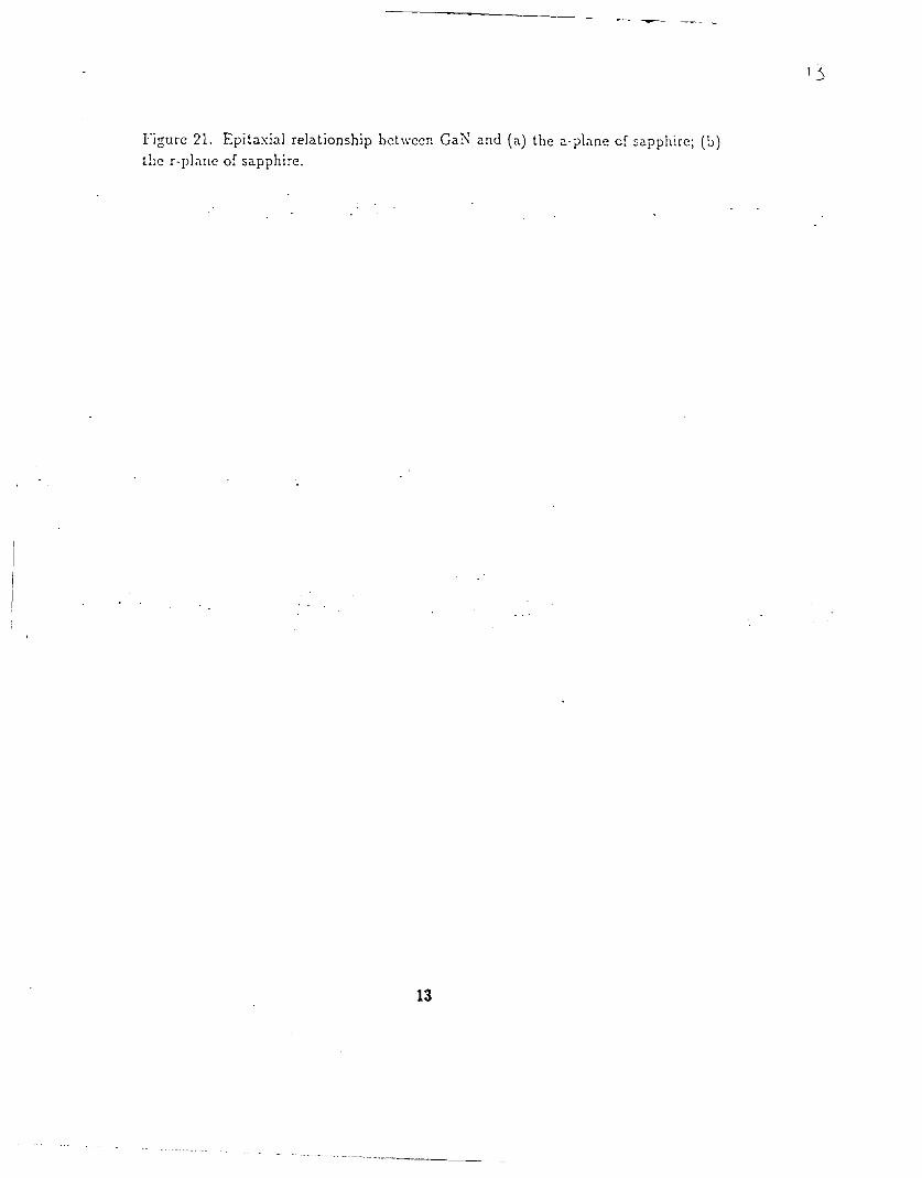
Figure 21. Epitaxial relationship between GaN and (a) the a-plane of sapplire; (b)the r-plane of sapphire.
13

00
ci.)
00CL m
wx
U,
ClO
uow
00w(

C'
4-$-
-100
0
C'))
0
E00
00' o C-
0
0 CL
o -C
0 UY0 20
110
0 as C)
I~C,
(ssn!D) lai asuQW' Q-X

I �I
7.0
-
C. *2-dfl
I

A --
*- m W.2 0 .t.0 .2 4-1*~ .)t
1 - � -
P-c
:1.
- � � -

cI P

I t
,:1d,
. 4.
- - $- --
_ii- i-_"-~fj~t
i .I

co
(CD
to.
CDU~
CD-
C\J
C) -) CD Ln C nCDLfl C'jCD Lfl CM
C5 6 6:(zs/sj~xnoDOr x) Slisua'uI
K-

LJn
CD
U-)
CD
C:)
co C
(*oas/sjuno:Dor x) kqlsuaqu

-) )
Q))
.0
;- A
Ln)
U-)
cD CD
CD Cfl C) C CD CI)
m (Ni W-4
(c~s/~unD)XllsualuI

(NJ
C.)
CD h-O
m
m
UD Ln-r mCD~(~ss~uoz)X11sualuj
1~C~2.
C:)
CMi
In
CD
bfl
CD
CD
In
C:)CDm D D D CDCD CD CD CD CD CDC)CD U- C ) CD IC)m CMC V-4 V-4
�bi..
0
�:¶y� �-ja��tW .:.
!4tabt
r
7 �flt'
-4--.-.V f. �
19
in
"-"C.-. .-.* - -
¾
£a
0pit
* -*--.., �
pitI.
-. . .. )- -- S �� ,�t*
-'½
-. t ***I***t*�**
*�,.crat:Ct' �v�.�rYjZ.z�AU' �:-� -
K

-- -.:14
0d

Cd

LO C)
coE
10
CCD
C> C) C) CDC ~u)CD 0 0 C CD
ta 0 t) CD LOc ~ jVJ
-oas/sluno
0 Q 0o0 0- 0LA
-oesslsunoo

* C)
E 0o
c~C)
C)G
it) 0o ito 0 itC)J 0 C it
-oas/slunoo
(\j
o C) C> C)oCCo0 0) C0 C0C)C0 0 0 C0 C0 C
0~ 0 0O00D
'0@S/slunoo

0D
C)
ao
11 01
C)o
a) 0 0 0 0 0 0 ao o ) 0 0 0 0) 04j- n 0 D Cl) a)J
-oasisiuno:: (
0
C)
C0 0 C ) C
C) C ) ) C ) C)
C\j 1
cOas/siunoo

S ) C)
04 c--.4 ;-4
-4-
0 Z tM4 C3C
S ~Ia
C, C- a C/
""-- --------'- ----------
0 N
V , .... .. .. . . "t . ..
X a n
"a!a
-a -a -------------
i a
a a
C-itI I
II a
< 2
Appendix B:
Heteropitaxy, Polymorphism And Faulting In GaN Thin Films on Siliconand Sapphire Substrates

C,-;
submitted for publication
Journal of Applied Physics
Heteroepitaxy, Polymorphism AndFaulting In GaN Thin Films OnSilicon And Sapphire Substrates
T. Lei' , K.F. Ludwig Jr.1 and T.D. Moustakasl'2
'Dept. of Physics, Boston University; Boston, MA 02215
2 Dept. of Electrical Engineering, Boston University; Boston, MA 02215
"Current Address: Dept. of Materials Science, North Carolina State University
Raleigh, NC 27695

Abstract:
The structure of GaN films grown by electron-cyclotron-resonance-assisted MBE on
Si(111), Si(001), basal-plane sapphire, a-plane sapphire and r-plane sapphire substrates was
studied with four-circle x-ray diffractometry. Phase content, domain size, inhomogeneous
strain and in-plane and out-of-plane domain misorientations were measured and compared
for films grown on each type of substrate. Wurtzite and zincblende polymorphs were
found to coexist in films grown on Si(111). The two structures grow in the (0002) and
(111) orientations respectively so that they may transform into each other via stacking
faults on close-packed planes. Smaller amounts of zincblende material were also found in
predominately (0002) wurtzitic films on a-plane sapphire and (1120) wurtzitic films on
r-plane sapphire.
|q
1. Introduction:
The growth and properties of GaN films have been under extensive investigation
because of their potential applications as light-emitting devices in the blue, violet and
near ultra-violet spectra [1,2]. It is known that GaN exists in two polymorphs: wurtzite
and zincblende structures with direct bandgaps of 3.4 eV and 3.2 eV respectively. The
two are analogous to hcp and fcc structures respectively in their stacking sequences. Since
bulk GaN substrates are not available, films must be grown by heteroepitaxy on foreign
substrates. The majority of CaN films reported have grown in the wurtzite structure, most
commonly with the basal planes parallel to the substrate. However, epitaxial stabilization
of the zincblende phase has been obtained on GaAs, MgO, SiC and Si substrates [see the
citations in Ref. 1]. All substrates used have a large mismatch to GaN films.
Despite the critical role which substrate symmetry and unit cell size must play in the
formation of heteroepitaxial GaN films, relatively little detailed coniparative structural
work has been performed. While reflective high-energy electron diffraction (RHEED) is
often used to characterize films in situ [3-6], it probes only the surface structure of the grow-
ing film. Electron transmission microscopy (TEM) studies provide important information
about the film microstructure and epitaxial orientation [7,8], but they cannot quantita-
tively examine the degree of orientational order between film domains or reliably detect
small phase components. In contrast, x-ray diffraction examines the structure of the bulk
of the film, can quantify the degree of film orientational order and can determine oriented
minor phase content down to the 10' level. However, x-ray diffraction measurements
limited to Bragg peaks from planes parallel to the substrate have significant limitations.
In these cases, experiments cannot distinguish between wurtzitic material in the (0001)
and (017O) orientations and zincblende material in the (111) and (110) orientations respec-
tively. Moreover, rocking curves of "on-axis" Bragg peaks [9) show only the orientational
order perpendicular to the substrate - they yield no information on the orientationsl order
of film domains in the plane.
We report here a comprehensive x-ray diffraction study examining both the in-plane
and out-of-plane structures of GaN films grown by electron-cyclotron-resonance-assisted
molecular beam epitaxy (ECR-MBE) on two of the most important substrates for tech-
nological applications - silicon and sapphire. Silicon substrates were of (111) and (001)
orientation. Sapphire substrates were of (0001) (basal-plane), (1100) (a-plane) and (1i02)
(r-plane) orientations. The details of the growth process have been previously reported
along with brief descriptions of some of the x-ray results [10-13]. All films studied here
were approximately one micron thick and included a thin (-,, 200 A) GaN buffer layer at
the substrate interface. We have found that wurtzite and zincblende GaN polymorphs
often coexist in films which grow with their close-packed stacking planes parallel to the
substrate. This may explain the variable optical and transport measurements sometimes
observed in GaN films [14].
2. Experimental Methods:
The x-ray diffraction measurements reported here used Cu K,, radiation in conjunc-
tion with a sagitally focussing graphite (002) monochromater crystal for low resolution
measurements and a Ge (111) crystal for high resolution work.
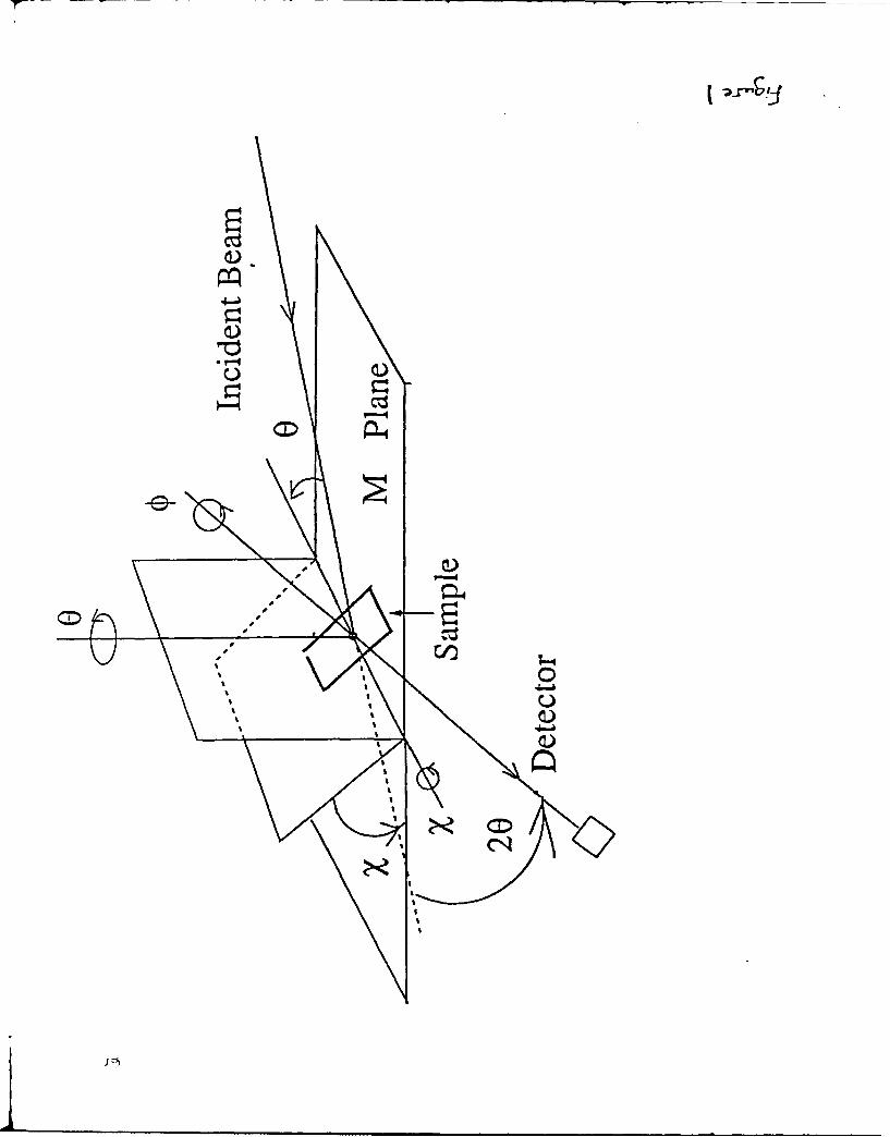
The experiments utilized a four-circle diffractometer which allowed access to a large
volume of reciprocal space [15]. A schematic of the four-circle geometry is shown in Fig. 1.
The horizontal plane M is the one defined by the incident and reflected beams; X is defined
as the angle between the sample surface and plane M and X = 0 when they are parallel.
The angle 0 measures the rotation around the surface normal of the substrate and 2P is
defined as the angle between the incident and reflected beam. The angle 0 measures the
sample rotation around the axis perpendiculer to the M plane.
Several different types of scans were utilized to characterize the thin films. The sim-
plest, e - 29 scans, measure the film structure along the surface normal fi, giving infor-
mation on phase presence and orientation. Homogenous strain in the film due to uniform
2

stress or nonstoichiometric composition is reflected in Bragg peak shifts relative to the
those expected from measured GaN lattice constants. Irhomogeneous strain and finite do-
main sizes act to broaden the 8 - 28 Bragg peak widths. In reciprocal space, the FWHM
width of a peak in a 8 - 28 scan includes both effects [161
2ir,k = '3 + "' (1)
where D is the average domain size and ei, is the inhomogeneous strain, i.e. the FWHM
variation of the interplanar spacing d through the film, 6d/d. Equation 1 assumes that the
peak broadening due to the instrumental resolution has been removed and that the finite
domain size and inhomogeneous strain contributions lead to lorentzian peakshapes. Vari-
ous factors can contribute to ei,,, including local stresses due to dislocations and mismatch
as well as "stress-free" strain due to varying chemical stoichiometry through the film.
As mentioned in the introduction above, 0 - 28 measurements do not uniquely de-
termine phase presence and orientation in CaN films because the (0002) or (1120) planes
of wurtzitic GaN films have virtually identical spacings and structure factors as do the
(111) and (220) planes of zincblende CaN respectively. Therefore, x-ray diffraction scans
at off-axis reflection peaks from planes inclined relative to the substrate were used in this
study to distinguish between the wurtzite and zincblende structures. For convenience, we
refer to these measurements as l-.cans if they were performed in the direction of the film
normal.
Measurements were also performed to examine the orientational quality of the thin
films. Rocking curves of 0 around the on-axis Bragg peaks were used to examine the
orientational spread of the film parallel to the surface normal. The spread of in-plane
orientations as well as the epitaxial relationship between substrate and film axes in the
plane were determined with 0 scans, in which the sample was rotated about its normal
while 9, 29 and X were held fixed at the peak postion.
3

3. Experimental Results:
3.1 GaN on Si
A. GaN on Si(111)
X-ray 0 - 20 scans of films on Si(ll1) show only two peaks which are indexed as the
wurtzite (0002) and/or zincblende (111) and their harmonic. The peak positions yield
a d-spacing of 2.59 A, which is consistent with previous lattice constant measurements
[1]. No other peaks were observed, ruling out the existence of other epitaxial orientations
down to the 0.1% level. Since data from only two peaks are available, the separation of
the peak widths into domain size and inhomogeneous strain broadening using Eq. (1) has
limited accuracy. However the theta FWHM of the fundamental peak and its harmonic are
0.08* and 0.19" respectively, implying that the dominant contribution to the widths comes
from an inhomogeneous strain of approximately 0.2%. The grain size estimated from the
peak widths is resolution limited, so that the coherent domain size must be larger than
approximately 1500 A.
In order to better investigate the polymorph content of the film, I-scans were per-
formed along the wurtzite (10i1), (1i01) and (1121) lines in reciprocal space (see Figs. 2 and
3). The scans show that there are significant components of both wurtzite and zincblende
phases in the materials. The zincblende further exists equally in its two twins correspond-
ing to ABCABC... and CBACBA... packing. The relative heights of the zincblende and
wurtzite peaks suggests that approximately 25% of the film is zincblende and the remain-
der is wurtzite. The in-plane orientation between the two polymorphs is wurtzite [1010] IIzincblende [jiO], which is the orientation required in order for the close-packed planes of
the two polymorphs to be in registry. It is noteworthy that earlier reports [17] of wurtzite
formation on Si (111) could not distinguish between wurtzite and zincblende structures,
so that similar polymorph coexistence way have been present there as well.
It is possible that the zincblende and wurtzite phases nucleate independently on the
4
substrate. However, in cobalt and silicon carbide [18] it is known that the two analogous
hcp and fcc polymorphs can nucleate each other at stacking faults on the close-packed
planes. Moreover, twinning in metallic crystals as well as in CdTe [19] films can occur
in the same way. It is therefore possible that the coexistence of the two polymorphs
and of the two zincblende twins in the GaN films may be related to the presence of
stacking faults. Approximate fault densities can be obtained from the widths of the off-
axis diffraction peaks, since faulting effects the broadening of different reflections unequa!l~.
Bragg peaks for which h-k=3n, where n is an integer, are unaffected by faulting along the
close-packing planes, while others are broadened in direct proportion to the density of
faults [201. Analysis of the wurtzite (115_4) and (1104) peak widths indicates that there
is an extra width associated with faulting and implies that the average distance between
faults is approximately 800 A. Although we cannot completely rule out other nucleation
mechanisms, TEM studies [21] performed after our initial reports of these results [22] have
shown conclusively that wurtzite and zincblende polymorphs do nucleate each other at
stacking faults in InN films.
In addition to the peaks which can be indexed to the wurtzite and zincblende struc-
tures, there is a very small peak not belonging to these two phases in the (1121) and (10D1)
scans at I = 1.66 reciprocal lattice units (r.l.u.). The position of a peak at a nonintegral I
value suggests that it could be due to a larger superstructure. Polytypes with long repeat
periods are well known in the silicon carbide system [18]. However, no other peaks at-
tributable to a long-period polytype are observed and calculations suggest that polytypes
would not have a strong reflection at this position. "'he origin of the peak therefore remains
unclcar.
The orientational quality of the films normal to the substrate was examined with erocking curves at the wurtzite (0002)/zincblende (111) peak (see Fig. 4). The FWHM of
the rocking curve, which is a direct measure of the orientational spread of grains around the
surface normal, is 0.9°. The orientational quality parallel to the substrate was measured
5

with 0 scans at the wurtzite (1i02) and zincblende (ill) reflections. The dominant peak in
the wurtzite (1i02) scan has the sixfold symmetry expected from the hexagonal structure.
However, very small peaks with slightly less than 1% of the intensity of the dominant peaks
were observed at 0=30° and 0=90°. These indicate that a small fraction of the domains
have an in-plane orientation which differs by 300 from the bulk of the wurtzite component.
Phi scans of the zincblende (ill) show that these 30° misoriented domains exist in that
polymorph as well (see Fig. 5). The in-plane orientational spread of the wurtzite film
component is 1.90, twice as large as the out-of-plane orientational spread. The epitaxial
in-plane orientation is GaN[11ý0] 11 Si[il0]. This is the same orientation as found in earlier
growth studies [17].
B. GaN on Si(001)
We have previously reported the results of 0 - 20 scans and rocking curves of GaN
films on Si(001) substrates [3,4]. The dominant peaks in the 0 - 20 scans are indexed to
zincblende (002) and (004). The large widths of the two peaks, 0.400 and 0.72° respectively,
indicate a higher inhomogeneous strain and a smaller domain size than occurs on the
Si(1I) substrate. Application of Eq. (1) yields an approximate inhomogeneous strain of
0.6% and a domain size of 500 A.
In addition to the dominant zincblende (002) peak and its harmonic, the 0 - 20 scan
shows a small peak at the position corresponding to zincblende (111) and/or wurtzite
(0002) orientations. Thus approximately 1% of the film has this orientation. Transmission
electron microscopy has shown that this component develops in the early stage of the buffer
layer deposition.
The rocking curve of the (002) peak is 1.6° wide - much broader than that of GaN
on Si(lll). The in-plane orientational order of the dominant zincblende (001) phase was
examined with a 4 scan of the (111) reflection. It shows a fourfold rotational symmetry
with a spread of approximately 2.5° about the maxima. The 4 scans show also that the
epitaxial relationship between film and substrate is GaN(100) [[ Si(100).
6

3.2. GaN on Sapphire Substrates
A. GaN on basal-plane sapphire
As was the case with the Si(111) substrate, the 0 - 20 scan of the GaN film on
basal-plane sapphire shows two dominant peaks correspondng to wurtzite (0002) and/or
zincblende (111) and their harmonic. Again, these values are in good agreement with
previously reported values. The widths of the two peaks are 0.06* and 0.11", from which
the grain size is estimated to be greater than 1500A and the homogeneous strain to be
approximately 0.8%.
In order to further examine the polymorph content of the film, we also searched for
(i11) reflections of (111) oriented zincblende grains. In contrast to the case for GaN grown
on Si(111), however, there is no zincblende (111) intensity down to the 10' level.
The 0-rocking curve of the film (0002) peak has a FWHM of 0.4*. This is comparable
to that observed by Sasaki and Zembutsu [23] in films grown with MOCVD and by Shintani
et aL 124] using HVPE, but significantly smaller than that in MOCVD films grown on AIN
buffers by Amano ct aL. [9]. Phi scans at the (1102) reflection (the off-axis peak) of GaN in
the wurtzite structure display the dominant reflection peak as ý rotates every 60 degrees,
a result of the 6/m symmetry of tire rotation axis, as is in the case on Si(1ll). However,
no in-plane misoriented domains were observed. The in-plane orientational spread is 0.80,
about twice as large as the out-of-plane orientational spread. The in-plane orientation of
the film is found to be GaIN (1120) 11 sapphire (li00). This is in agreement with previous
reports on CaN films on basal-plane sapphire grown by a variety of techniques [3,4,5,6,25].
The lattice mismatch between GaN and the basal plane of the sapphire hexagonal unit cell
is over 30%. However, as noted by Kosicki and Kahng 14], the mismatch is significantly
less (-, 15%) between the wurtzite basal plane unit cell and a smaller hexagonal cell
within the sapphire unit cell. The smaller cell of Al atoms on the basal-plane sapphire is
oriented 30* away from the larger sapphire unit cell, in agreement with the CaN orientation
found experimentally. Figure 6 shows that this epitaxial orientation gives relatively good
7
agreement between the bulk atomic pritiorn Al atoms in the sapphire and Ga atc
in the film.
B. GaN on a-plane sapphire
As is the case for GaN grown on Si( 11) and basal-plane sapphire, 9- 20 scans of G
film on a-plane sapphire show peaks corresponding well to previously published values
the wurtzite (0002) interplanar spacing. The FWHM of the two peaks are 0.060 and 0.1
the same as those for GaN on c-plane sapphire, so that the grain size and inhomogenet
stress are similar. The zincblende (111) peak was examined to measure the percentz
of (111) oriented cubic phase present. The peak's intensity suggests that approximat
1% of the material has the zincblende structure. A previous examination by Wickenc
et al. 1251 of GaN films deposited by vapor phase epitaxy had reported only the grom
of wurtzitic material. It is unclear, however, that the study could distinguish between t
wurtzite and zincblende polymorphs.
Although the domain size and inhomogeneous strains of the GaN film grown on
plane sapphire are similar to those for films grown on basal-plane sapphire, the 0-rocki
curve of the film on a-plane sapphire has a FWHM of 0.60, 50% larger that that of G:
on basal-plane material. Phi scans at the off-axis wurtzite (1102) reflection show no:
plane misoriented domains, as is the case with basal-plane sapphire. However, the in-plL
orientational spread here is significantly larger - 1.48. The in-plane epitaxial re.ationsh
was found to be GaN [1120] II sapphire [liOOJ. As Wickenden ei al. [25] point out,
this orientation the bulk positions of the substrate and film cations lie along lines in t
sapphire 10001] direction (see Fig. 7). The mismatch between the substrate and film -,
spacings is only ,.0.7%, although many of the substrate and film cation positions do r
show a good correspondance.
C. GaN on r-plane sapphire
When 9 was aligned with respect to the GaN reflection, 9 - 29 scans from films grov
8

on r-plane sapphire showed only a peak which is indexed to the (1120) reflection. No peak
from the sapphire substrate was observed. However, when 0 was aligned with respect to
the substrate reflection, the scan showed only the sapphire (22504) peak. Thus the film
planes are not exactly parallel to the (1102) planes of the sapphire substrate. By varying
q, it was found that the misorientation is approximately 1.50 and is along the GaN [0001]
direction. In order to better measure the phase content of the films, we examined the
zincblende (111) off-axis peak. From its peak intensity, we estimate that only -- 1% of the
materials is in the zincblende phase; the remainder is wurtzite. Again, previous studies
have reported only the growth of wurtzitic GaN on r-plane sapphire [3,5,22], but it is
unclear that they had the ability distinguish between the two polymorphs.
The FWHM of the 0 rocking curve at the on-axis peak is 0.60. This is comparable
to values reported by Sasaki and Zembutsu [22] on films grown by MOCVD. In order to
examine the in-plane orientation, a 0 scan was performed at the wurtzite (1100) reflection.
The scan shows a repetition every 1800 in 0, which is a result of the 2-fold symmetry
of a-plane GaN. The in-plane orientational spread is 6.7%, the largest for all of the GaN
films. Phi scans show that the in-plane orientations between the two film polymorphs
and the substrate are wurtzite (0002) 11 sapphire (1101) II zincblende (lil). The wurtzite
epitaxial orientation is the same as that found in previous reports of films grown on r-
plane sapphire [3,5,22]. Surface studies have found that corundum r-plane surfaces are
quite stable and evidently do not significantly reconstruct 1261. It is therefore interesting
to note the relatively good agreement between bulk substrate and film cation positions
in the experimental epitaxial orientation, as Fig. 8 shows. The lattice mismatch is only
1.3% in the sapphire [1101] direction, although it is -15% in the [11120] direction. The
particularly small mismatch in the sapphire [ 1011 direction may be responsible for the
small tilt between the GaN planes in the film and the substrate planes. Since the film axis
in this direction is slightly longer than that of the substrate, the film planes may tilt up
slightly in order to better match the projection of the GaN unit cells onto the interface with
9

the sapphire unit cells below. Because of the two-fold rotational symmetry of the sapphire
r-plane unit cell, however, it is unclear why film domains grow with a misalignment in only
one of the two possible directions. An alternate possibility is that the film tilt is related
to a miscut of the substrate wafer. However, the tilt was observed in several films and was
always oriented along the sapphire [1101] direction.
4. Discussion and Conclusions:
The results of our four-circle x-ray diffractometry suggest that the coexistence of
wurtzite and zincblende polymorphs in GaN thin films may be widespread. As discussed
above, most previous studies would not have been able to distinguish between the two, es-
pecially if one polymorph exists only at the 1% level. Since the two have different bandgaps
and possibly different doping capabilities, it is imperative that future investigators inter-
ested in optical and transport properties also evaluate their films' phase contents. For this
purpose x-ray or electron diffraction measurements of off-axis Bragg peaks are both suit-
able, but x-ray diffraction may have somewhat greater sensitivity to small volume fractions
and it requires no sample thinning.
To our knowledge, these are the first experiments which have examined the orienta-
tional quality of GaN films in the film plane. On all of the films, the range of orientation
angles in the plane is 1.5 to 10 times times larger than along the film normal. In-plane
misorientations between domains may therefore be the more important in creating domain
boundary recombination sites due to broken bonds.
It is noteworthy that the measured film lattice constants in this work are all equal
to accepted literature values to within experimental error. Since the lattice paramater
is sensitive to the nitrogen concentration [271, this implies that the films' compositions
are not too far off stoichiometry. We have, however, observed significant variations in
CaN lattice paramaters with varying growth temperature which we attribute partly to
the formation of large numbers of nitrogen vacancies 1281. It is widely believed that such
10

nitrogen vacancies autodope films n-type [1]. The agreement between previously reported
lattice constants and those observed here also suggests that the interfacial strain in the
films relaxes on length scales significantly smaller than the film thickness. Given the
large mismatches present between substrate and film, this is not suprising. For GaN on
Si(111) and Si(001) substrates the lattice mismatch is 6=21%. As Figs. 6-8 show, however,
films grown on sapphire orient themselves to match the bulk atomic positions of the film
and substrate and decrease the effective lattice mismatch below the values for epitaxy on
silicon. We note that, in fact, the GaN films do not grow directly on the sapphire substrate
surfaces, but rather on very thin AIN layers which grow during the substrate N2 plasma
cleaning process [13]. However, the AIN lattice constant is quite close to that of GaN
(3.11 A versus 3.19 A) and our RHEED measurements indicate that the AIN has the same
orientation as does the GaN film which grows on top of it. Unfortunately, the detailed
structure of the film-substrate interface is unknown so the importance of matching bulk
atomic positions in the early stages of film growth is unclear. Despite the reasonably good
match of cation positions in the GaN films grown on r-plane sapphire, for example, the
orientational spread in the film plane is quite large. Clearly a better understanding of the
early growth kinetics and of the interfacial structure would be quite helpful in explaining
the epitaxial relationship between film and substrate.
The dominant mechanisms causing the inhomogeneous strains measured in these ma-
terials are unclear. Since the films appear to relax quickly to their bulk lattice paramater
and are relatively thick, it is unlikely that e,, could be dominated by misfit stresses from the
substrate interface. However, dislocations introduced to relieve the lattice mismatch could
create microstresses which would cause local variations in the lattice constant. While we
know of no experimental work relating the GaN bandgap to the lattice paramater, LCAO
calculations suggest that the energy matrix elements V which determine the bandgap vary
as the inverse square of the separation between atoms [29). Therefore bV/V = 26d/d, and a
1% inhomogeneous strain would lead to approximately a 2% variation of the bandgap. This
11
then could be a significant source of band tailing. Nitrogen vacancies would presumably
be the principal mechanism contributing "stress-free" strain due to composition inhomo-
geueity. -While a decrease nintrogen stoichiometry significantly decreases the wurtzite
lattice paramaters [27], we know of no quantitative data relating stoichiometry and lattice
constants which would allow us to interpret the inhomogeneous strain in terms of nitrogen
deficiencies.
All of the films except those on Si(001) have domain sizes along the surface normal
which are larger than our instrumental resolution. The relatively small size of domains in
GaN films on Si(001) along with their large spread of in- and out-of-plane orientation angles
and relatively large inhomogeneous strain suggest that, structurally, these are the worst
films overall. The very large spread of in-plane orientations in the films on r-plane sapphire
also implies that there are domain boundaries within the film with a relatively large angle
of mismatch. In terms of orientation quality and domain size, then, the best films appear to
be those which grow on their dose-placked planes. The films on sapphire (0002) substrates
are the best of these, with relatively small in- and out-of-plane misorientation and little
secondary phase. Despite their orientational quality, however, stacking faults may be
common in all of the materials grown in the close-packed orientation. The impact of
stacking faults on carrier mobility is unclear. Away from fault edges, their main effect will
likely be to cause a local variation in the bandgap. At the fault edges, however, bonds will
be broken, producing deep states in the gap. Clearly significant work is required in order
to examine the relationship between stacking fault density and electrical properties and to
develop approaches which minimize the formation of faults in the growth process.
Acknowledgments
We would like to thank G. Morales and Y. Xie for their help with the x-ray measure-
rments. This work was supported by the Office of Naval Research (Grant No. N00014-92-
J-1436).
12
References
1.- R. F: Davis, Proceedings of the IEEE.,.V. 79, No. 5, 702(19 9 1); R. F. Davis, Z. Sitar,
B. E. Williams, H. S. Kong, H. 3. Kim, J. W. Palmour, 3. A. Edmond, J. Ryu, J. T.
Glass and C. H. Carter, Jr., Mat. Sci. & Eng. B1, 77(1988).
2. J. I. Pankove, Mat. Res. Soc. Syrup. Proc. 162, 515 (1990).
3. M. Sano and M. Aoki, Jap. J. App. Phys. 15, 1943 (1976).
4. B.B. Kosicki and D. Kahng, J. Vac. Sci. and Tech. 6, 593 (1969).
5. S. Yoshida, S. Misawa and S. Gonda, J. Appl. Phys. 53, 6844 (1982).
6. S. Yoshida, S. Misawa and S. Gonda, Appl. Phys. Lett. 42, 427 (1983).
7. Z. Sitar, M.J. Paisley,, B. Yan and R.F. Davis, Mat. Res. Soc. Symp. Proc. 162,
537 (1990).
8. T.P. Humphreys, C.A. Sukow, R.J. Nemanich, J.B. Posthill, R.A. Rudder, S.V. Hat-
tangady. and R.J. Markunas, Mat. Res. Soc. Syrup. Proc. 162, 531 (1990).
9. H. Amano, N. Sawaki, I. Akasaki and Y. Toyoda, Appl. Phys. Lett. 48, 353 (1986);
1. Akasaki and H. Amano, Mat. Res. Soc. Symp. Proc. 242, 383 (1992).
10. T. Lei, M. Fanciulli, R. J. Molnar, T. D. Moustaklas, R. J. Graham and J. Scanlon,
Appl. Phys. Lett. 58, 944 (1991).
11. T. Lei, T. D. Moustakas, R. J. Graham, S. J. Berkowitz and Y. He, J. Appl. Phys.
71, 4933 (1992).
12. T. Lei, T. D. Moustakas, Mat. Res. Soc. Symp. Proc. 242, 433 (1992).
13. T. D. Moustakas, R. I. Molnar, T. Lei, G. Menon and C. R. Eddy, Jr., Mat. Res.
Soc. Symp. Proc. 242, 427 (1992).
14. T. Lei and T. Moustakas, to be published.
15. W. R. Busing and H. A. Levy, Acta Cryst. 22, 457 (1967).
13

54c
16. R.W. Vook, in Epitazial Growth, ed. J.W. Matthews (Academic Press, New York,
1975), 339.
17. Y. Morimoto, K. Uchiho and S. Ushio, J. Electrochem. Soc. Solid-State Sci. and
Tech. 120, 1783 (1973).
18. R.W.G. Wyckoff, Crystal Structures, Vol. I (Interscience, New York, 1963), 111.
19. R.D. Homing and J.-L. Staudenmann, Appl. Phys. Lett. 49, 1590 (1986).
20. B.E. Warren, X-ray Diffraction (Addison-Wesley, Reading, 1969), 275.
21. S. Strite, D. Chandrasekhar, D.J. Smith, J. Sariel, H. Chen, N. Teraguchi, and H.
Morko, preprint.
2% T.D. Moustakas, T. Lei and R.J. Molnar, Physica B, in press.
23. T. Sasaki and S. Zernbutsu, J. Appl. Phys. 61, 2533 (1987).
24. H. Shintane, Y. Takano, S. Minagawa and M. Mari, J. Electrochem. Soc. 125, 2076
(1978).
25. D.K. Wickenden, K.R. Faulkner, R.W. Brander and B.J. Isherwood, J. Cryst. Growth
9, 158 (1971).
26. V.E. Henrich, Rep. Prog. Phys. 48, 1481 (1985).
27. 0. Lagerstedt and B. Monemar, Phys. Rev. B 19, 3064 (1979).
28. C.R. Eddy, Jr, T.D. Moustakas and J. Scanlon, J. Appl. Phys. 73 (1993), in press.
29. W.A. Harrison, Electronic Structure and the Properties of Solids (W.H. Freeman, San
Francisco, 1980), 149.
14

Figure Captions
1. Schematic of the Eulerian four-circle diffraction geometry.
2. Schematic of reciprocal space showing an I-scan along the wurtzite (10D!) direction.
The dots are allowed wurtzite reflections and the triangles show the allowed zincblende
reflections for each of the two twins (primed and unprimed). The off-axis zincblende
reflections are labelled with respect to the cubic cell, but the graph units are wurtzite
reciprocal lattice units (r.l.u.).
3. An f-scan along the wurtzite (10l) direction. The I reciprocal lattice unit values refer
to the wurtzite c-axis and the wurtzite and zincblende peaks are labeled. As discussed
in the text, the origin of "peak x" at 1.66 r.l.u. is unclear.
4. A € scan at the wurtzite (li02) peak for a film on Si(111).
5. A 5 scan at the zincblende (Ill) peak for a film on Si(111).
6. Projection of bulk basal-plane sapphire and GaN cation positions for the observed
epitaxial growth orientation. The dots mark aluminum atom positions and the dashed
lines show the sapphire basal-plane unit cells. The open squares mark gallium atom
positions and the solid lines show the GaN basal-plane unit cells. The aluminum
atoms on the sapphire plane sit at positions approximately 0.5 A above and below the
plane position.
7. Projection of bulk a-plane sapphire and basal-plane GaIN cation positions for the
observed epitaxial growth orientation. The dots mark aluminum atom positions and
the dashed lines show the sapphire a-plane unit cell. The open squares mark gallium
atom positions and the solid lines show the CaN basal-plane unit cells.
8. Projection of bulk r-plane sapphire and a-plane CaN cation positions for the observed
epitaxial growth orientation. The dots mark aluminum atom positions and the dashed
lines show the sapphire r-plane unit cell. The open squares mark gallium atom posi-
tions and the solid lines show the CaN a-plane unit cells.
15
4-J
a> 0
SN

AI-scan n
i-scan1 (r.l.u.)A
4z(1 13)' 3z(022), 3
X 2z(002)'z(1l 1•
1 0(10711 (ooo0o

10 C61,-4 C\
V _6
-, C\2 OOv
0 D4 m
cd o
10~
100
0 1 2 3 4 5

11
CD
CQ C')
[Das/sjunoo] 4C1su~nuj

LO
W3
J4
h0
[oos/slunoo] CllmaltU

GaN [10001t Sap.3hirc [1010]
GaN (01 101Sapphire (1010]
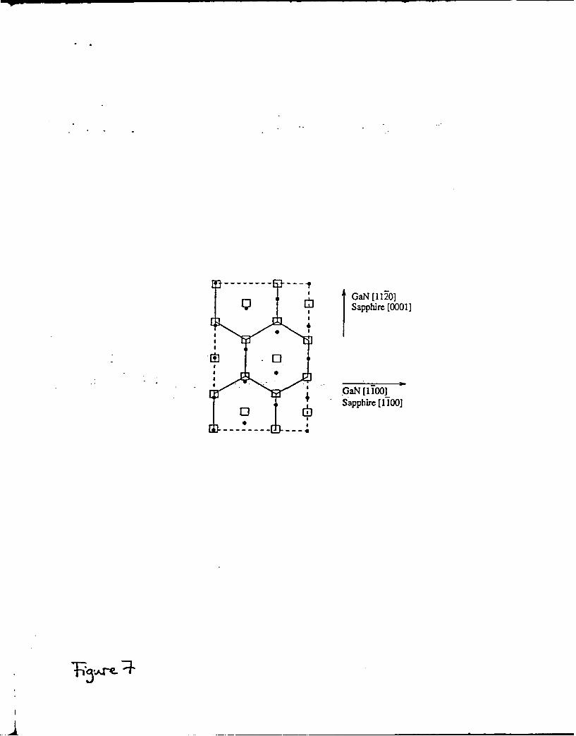
5 1Sapphire [0001]
I
4 GaNI11100
0 Sapphire [1100]

3 x5.18X GaaN [1100 _I Sapphire [ 1120]
5.52X BIJ [] [] 4.75
..t ------- t - - ---- GaN [00011
-Sapphire [IT]0 1
S II

Appendix C:
Electron Transport Mechanism in Gallium Nitride

to be published:
Applied Physics Letters, Jan. 1993
Electron Transport Mechanism in Gallium Nitride
R.J. Molnar, T. Lei and T.D. Moustakas
Molecular Beam Epitaxy Laboratory, Department of Electrical Computer and Systems
Engineering, Boston University, Boston, MA 02215, U.S.A.
ABSTRACT
The electron transport mechanism in autodoped Gallium Nitride (GaN) films grown by Electron Cyclotron
Resonance microwave plasma-assisted Molecular Beam Epitaxy (ECR-MBE) was investigated by studying
the temperature dependence of the Hall coefficient and resistivity on samples with various concentrations of
autodoping centers. The Hall coefficients go through a maximum as the temperature is lowvered from 300
K and then saturate at lower temperatures. The resistivities in the same temperature range initially increase
exponentially and then saturate at lower temperatures. These findings are accounted for if a significant
fraction of electron transport, even at room temperature, takes place in the autodoping centers and that
conduction through these centers becomes dominant at lower temperatures. T77e activation energy of these
centers was found to be on the order of 20-30 meV. When the concentration of the qutodoping centers
becomes smaller than that of deep compensating defects, the material becomes semi-insulating and transport
by hopping in the compensating defects becomes dominant.
PACS # 72.20.Fr, 72.60.+g, 72.80.-r, 72.80.Ey

3;
Gallium Nitride (GaN) is one of the most promising wide-bandgap semiconductors for the
development of high efficiency UV-vis photonic devices due to its direct bandgap. The majority
of reported work indicates that the GaN films are autodoped n-type, a result generally attributed to
nitrogen vacancies"':. In general, the defect structure of GaN films is poorly understood and very
difficult to control experimentally, resulting in difficulties in doping this material p-type: 3.
GaN films produced by a variety of deposition methods were generally found to have low
electron mobilities (<100 cmrN/- s) and high carrier concentration (>10" cm"3) 2.3, although there
have been reports4 5 of mobilities -600 cmN- s and carrier concentration l10'6 cm 3 . Some other
workers"'7 reported semi-insulating films. One would expect that more lightly doped films would
have higher Hall mobilities. However, such films generally do not have measurable Hall coefficients,
suggesting low carrier mobilities,6" while highly conductive (even degenerate) samples readily have
mobilities > 20 cm/V- s. This anomoly has not yet been accounted for.
In this letter, we report on Hall measurements performed on a number of GaN thin films
grown on the (0001) plane of sapphire by the Electron Cyclotron Resonance microwave plasma
assisted Molecular Beam Epitaxy (ECR-2MBE) method. The data is analyzed by taking into account
that conduction through defects makes a significant contribution to the electrical transport. The
proposed model also accounts for the low mobility in the semi-insulating films.
The films were deposited by the two step growth process in which a GaN buffer is grown
first at relatively low temperatures and the rest of the film is grown at higher temperatures7 ":. This
method is capable of producing either conductive or insulating films. The conductive films, which
are reported here, are generally grown under conditions (high substrate temperature, low nitrogen
overpressure) which are believed to lead to the introduction of nitrogen vacancies"'2 . These films
tend to be covered at the end of the run with microscopic Ga droplets, due to phase separation of
excess Ga in the GaN films. To study the transport properties in these films the Ga droplets are
etched by emersing them in concentrated HCL. The insulating films, which are grown at high
nitrogen overpressure are free of Ga droplets.
The structure and surface morphology of these films were reported elsewhere'0 . X-ray
diffraction studies indicate that the films are high-quality single crystals with full width at the half
maximum of the 0-rocking curves found to be -10-20 min.
The films were grown at a deposition rate of 0.2 pm/h and were 1-2 pm thick. The samples
were abrasively etched into Van der Pauw lamilla and ohmic contacts were made by annealing
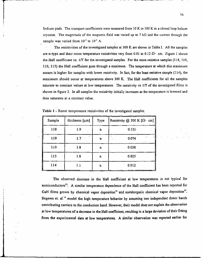
3'
Indium pads. The transport coefficients were measured from 10 K to 300 K in a closed loop helium
cryostat. The magnitude of the magnetic field was varied up to 7 kG and the current through the
sample was varied from 10.' to 10-3 A.
The resistivities of the investigated samples at 300 K are shown in Table I. All the samples
are n-type and their room temperature resistivities vary from 0.01 to 0.12 !" cm. Figure 1 shows
the Hall coefficient vs. I/T for the investigated samples. For the more resistive samples (118, 119,
110, 115) the Hall coefficient goes through a maximum. The temperature at which this maximum
occurs is higher for samples with lower resistivity. In fact, for the least resistive sample (114), the
maximum should occur at temperatures above 300 K. The Hall coefficients for all the samples
saturate to constant values at low temperatures. The resistivity vs l/T of the investigated films is
shown in figure 2. In all samples the resistivity initially increases as the temperature is lowered and
then saturates at a constant value.
Table I - Room temperature resistivities of the investigated samples
Sample thickness [fpm] Type Resistivity @ 300 K [n- cm]
118 1.9 n 0.121-
119 1.7 n 0.074
110 1.8 n 0.038
115 1.8 n 0.025
114 1.1 n 0.012
The observed decrease in the Hall coefficient at low temperatures is not typical for
semiconductors' 3. A similar temperature dependence of the Hall coefficient has been reported for
GaN films grown by chemical vapor deposition" and metalorganic chemical vapor deposition15 .
Ilegems et. al."' model the high temperature behavior by assuming two independent donor bands
contributing carriers to the conduction band. However, their model does not explain the observation
at low temperatures of a decrease in the Hall coefficient, resulting in a large deviation of their fitting
from the experimental data at low temperatures. A similar observation was reported earlier for
p-type and n-type Ge'6 , where a model involving transport in both the defect centers and the
conduction band was introduced to explain the phenomenon. The conduction in the defect centers
may be either diffusive, due to the small but finite overlap of the localized electron wavefunctions
of the defect centers or hopping' 7. Therefore the defect band mobility is expected to be small
compared to the conduction band mobility, and defect band conduction only becomes dominant
when carriers in the conduction band become negligible.
The results of Figs. 1 and 2 can be fined to such a two band model in order to determine
the relative concentration and the corresponding mobilities of electrons in the autodoping centers
and the conduction band. Let us assume that the donor concentration in our films is Nd, with an
activation energy AE,, and that the concentration of deep compensating centers (due to defects such
as dislocations) is N.. At a given temperature, a portion of the net carrier concentration (Nd-N.) is
excited into the conduction band and has mobility g, and concentration no. The unexcited carriers
remain in the defect states with a much lower mobility Wd and concentration nh. The net carrier
concentration of the conducting carriers is:
N.=n+ 'nd=Nd-N, (1)
Taking both these conduction mechanisms into account, the Hall coefficient, RH can be expressed16as.
an- 2 •+ (N,-n,) g 22
RH- -- C N~ Pd (2)(neP,+ (N,-nd) Pd) 2e
and the measured resistivity is
p 1 (3)a ncelic+ (N,-ne) epd
Letting b =d'lk, we have
(1 -b 2) n,+N~b2 (4)eRN= ((i-b) n,+Nb) 2
P=lt(i-b) n,+Nob) e(5
Note that if n, is much larger than n, (the high temperature limit), or g, = 0 ( the defect states do
not conduct) the expression for R. reduces to the expression used for one band conduction.
However, for g,,# 0, as the temperature is lowered the carriers in the conduction band will decrease
to the point where conduction through the defect states will dominate. It is also apparent from
Eqn.(4) that eRH at both temperature limits is the same and equal to 1iN0 . If b is not a strong
function of temperature, it can be shown that eR, in Eqn.(4) has a maxima
eRS - (1+b) 2 (6)4Nob
when
- Nob (7)
Therefore, the expression of RH in Eqn.(4) qualitatively predicts the shape of the experimental curves
shown in Figure 1.
The parameters p,, A, n, and nd are related to RH and p by equations (4) and (5). However,
at each temperature, there are three unknowns for the two equations. Hung et. al."6 approached the
problem by assuming that the measurements at high temperatures were dominated by the conduction
band electrons and extrapolated the carrier concentration curve to low temperatures to predict n, at
low temperatures. However, we found that in our case, the defect band conduction is not negligible
even Pt room temperature and therefore we did not adopt this approach.In the case of a well defined activation energy AE., the carrier concentration in the
conduction band is expected to change exponentially with temperature. The parameters N0,AEi, and
Al, Ad at each temperature can be extracted using equations (4)-(7) 12. The extracted values of No
and AEd for each cf the samples are listed in Table II.
Figure 3 shows the temperature dependence of p, and A~d calculated for sample 119. The
temperature dependence of A, is typical of semiconductors. The scattering is dominated at lowtemperatures by ionized impurities and at high temperatures by phonon scattering. The temperature
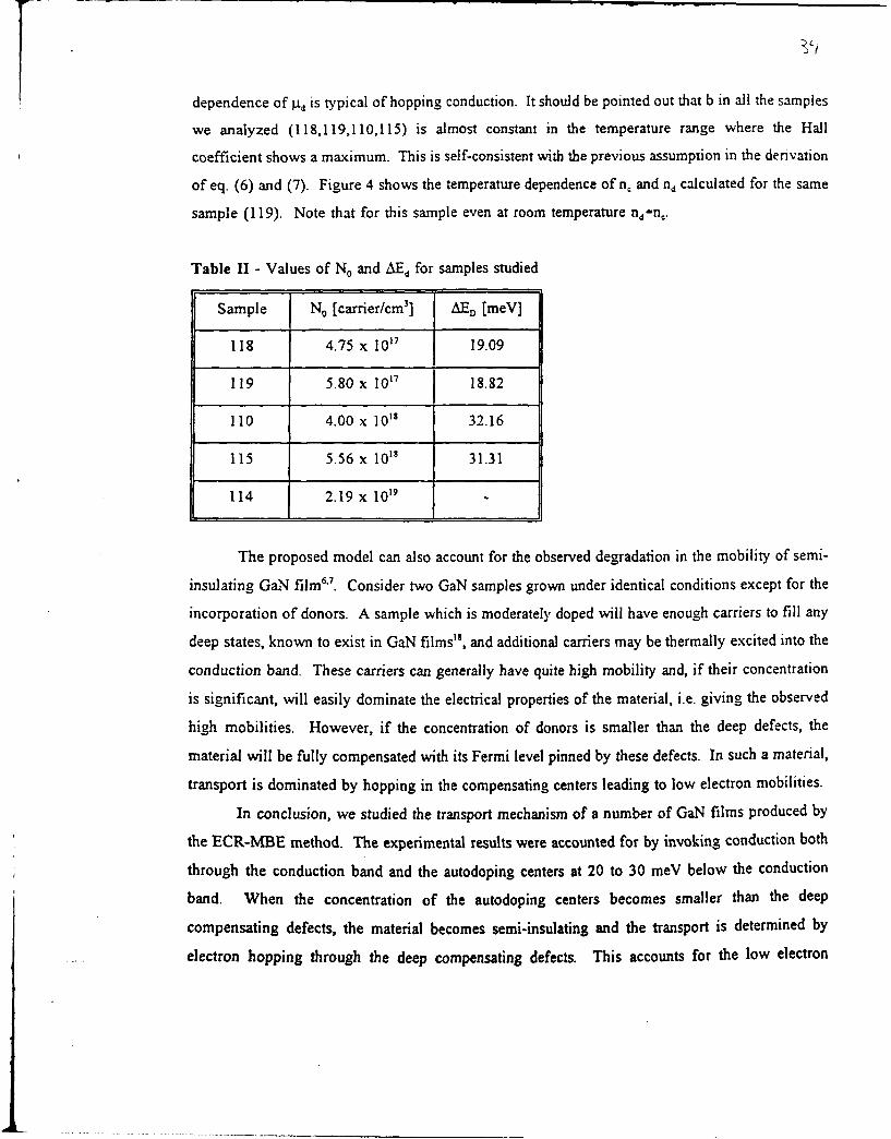
KCdependence of ýi, is typical of hopping conduction. It should be pointed out that b in all the samples
we analyzed (118,119,110,115) is almost constant in the temperature range where the Hall
coefficient shows a maximum. This is self-consistent with the previous assumption in the derivation
of eq. (6) and (7). Figure 4 shows the temperature dependence of n, and nd calculated for the same
sample (119). Note that for this sample even at room temperature nd-nC.
Table II - Values of No and AEd for samples studied
Sample N. [carrier/cm3 ] AE, [meV]
118 4.75 x 10¹⁷ 19.09
119 5.80 x 10¹⁷ 18.82
110 4.00 x 1 01S 32.16
115 5.56 x 10" 31.31
114 2.19 x 10'9 -
The proposed model can also account for the observed degradation in the mobility of semi-
insulating GaN film 6"7. Consider two GaN samples grown under identical conditions except for the
incorporation of donors. A sample which is moderately doped will have enough carriers to fill any
deep states, known to exist in GaN films", and additional carriers may be thermally excited into the
conduction band. These carriers can generally have quite high mobility and, if their concentration
is significant, will easily dominate the electrical properties of the material, i.e. giving the observed
high mobilities. However, if the concentration of donors is smaller than the deep defects, the
material will be fully compensated with its Fermi level pinned by these defects. In such a material,
transport is dominated by hopping in the compensating centers leading to low electron mobilities.
In conclusion, we studied the transport mechanism of a number of GaN films produced by
the ECR-MBE method. The experimental results were accounted for by invoking conduction both
through the conduction band and the autodoping centers at 20 to 30 meV below the conduction
band. When the concentration of the autodoping centers becomes smaller than the deep
compensating defects, the material becomes semi-insulating and the transport is determined by
electron hopping through the deep compensating defects. This accounts for the low electron

mobility of the semi-insulating GaN films. The nature of the autodoping centers is assumed to be
nitrogen vacancies, and their energy levels are found to be 20-30 meV. The compensating defects
are assumed to be due either to impurities or dangling bond related defects in dislocations.
We would like to thank M. Yoder for his encouragement in this effort- This work was
supported by the Officc of Naval Research (Grant No. N00014-92-J-1436).
1. H. P. Maruska and J. J. Tietjen, Appl. Phys. Lett. 15, 327 (1969).
2. J. I. Pankove, MRS Symp. Proc., 162, 515 (1990).
3. R. F. Davis, Proc. IEEE., 79, 702 (1991).
4. M. Ilegems, J. Cryst. Growth 13/14, 360 (1972).
5. S. Nakamura, Jpn. J. Appl. Phys. 30, L1705 (1991).
6. RtC. Powell, G.A. Tomasch, Y.W. Kim, J.A. Thornton and J.E. Greene, MRS Symp. Proc., 162,
525 (1990).
7. G. Menon, MS Thesis, Boston University (1990).
8. T. Lei, M. Fanciulli, R. J. Molnar, T. D. Moustakas, R. I. Graham and J. Scanlon, Appl. Phys.
Lett., 59, 944 (1991).
9. T. Lei, T. D. Moustakas, R. J. Graham, Y. He and S. J. Berkowitz, 1992a, J. Appl. Phys., 71,
4933 (1992).
10. T. D. Moustakas, T. Lei, R. J. Molnar, accepted for publication in Physica B.
11. T. D. Moustakas, R. J. Molnar, T. Lei, G. Menon and C. R. Eddy Jr., MRS Symp. Proc., 242,
427 (1992).
12. T. Lei, PhD Dissertation, Boston University (1992)
13. C. Kittel, Introduction to Solid State Physics, 6th Ed., J. Wiley & Sons, New York, 1986.
14. M. Ilegems and H. C. Montgomery, J. Phys. Chem. Solids, 34, 885 (1973).
15. I. Akasaki and H. Amano, MRS Symp. Proc. 242, 383 (1991).
16. C. S. Hung and J. R. Gliessman, Phys. Rev., 96, 1226.
17. N. F. Mott and T. D. Twose, Advances in Physics, 10, 107 (1961).
18. T. L. Tansley and R. J. Egan, MRS Symp. Proc., 242, 395 (1992)

Temperature-[K]
300 40 20 13.3100 '
,,,,-+ +
4 + +118
E lo: • 119H10
0
E -C[I M 0 CIO C 0110
1* * *115
)kCXXXXX xx x x x x x 114
0.1 00 25 50 75
1 OOO/T [K']
Figure 1 - Hail coefficient vs. 1/T.

Temperature [K]300 40 20 13.3
101
J
. . + 118
+ •
E 3 + +
.•XXXXXX xxx x x x x 114
0 + 55070.01: if 0' LL 0 0 01
looo/T [K7']
Figure 2 - Resistivity vs. /"T.

1000
S..~U AAA A~khA
E A
S100- gmeas A
.0 A
. ,•,9d i i00
000
10¾
10 10O0 1000Temperature [K]
Figure 3 - Temperature dependence of pX.g and g,.
y.0

7'
1018
A sse00 nA A
C-t
AAnmeas AAAAAA AA
0A
A
Temperature [K]
Figure 4 - Temperature dependence of n.,,., n, and rnd.
.C.
lA0 A
|C

Appendix D:
Metal Contacts to Gallium Nitride

submitted for publication
Applied Physics Letters
Mletal Contacts to Gallium Nitride
J.S. Foresi and T.D. Moustakas
Boston University, Department of Electrical Engineerin,
44 Cummington St., Bostor MA 02215.
AbstractWe report measurements on the nature of aluminumn and gold contacts to GaN.. The Ga.N
firns were deposited onto the R-plane of sapphire substrates by Molecular Beam Epitaxyand are autodoped n-type. Metal contacts were deposited by evaporation and were pat-terned photolithographically. Current-voltage characterization shows that the as-depositedaluminum contacts are ohmic while the as-deposited gold contacts are rectifying. The gold
contacts become ohmic after annealing at 575°C, a result attributed to gold diifusion. Thespecific contact resistivity of the ohmic aluminum and gold contacts were found by t:ansfer
length measurements to be of device quality (i1- 0 - I0- Pm2). The reslts of these studies
suggest a direct correlation between barrie: height and work function of the metal. r•s' ren.
"with the strong ionic character of GaN.
IntroductionGallium Nitride (GaN) is a direct, wide band-gap semiconductor (Z, s_ 3.1eV) whoIse
conduction band structure allows for a high saturation velocity (3 x 107 cm/sec) [1,21. D-e
to these unicue prooert.es Ga'N- is expected to find applilcations in optical devices (LED's,
lasers, detectors) operating in the spectzal region from the blue to near-UV anc in eiecrzoric
devices such as high temperature, high power, and high frequency transistors.
GaN films have been deposited heteroepit a:dally on a variety of substrates by a number of
vap or phase methods [3]. Such films are generally n-type with carrier concentrations between
1018 and 102' cm-' and electron moblities of about 20 cm 2/V.sec. The n-type autodoping is
attributed to nitrogen vacancies. The most important recent development is the discovery
that A1N[4] and GaN[5-9] buffers lead to lateral growth which significantly improves the
surface morphology and the electrical propeities of the films. For example, films with carrier
concentrations of 1016 and 1017 cm-3 and electron mobilities of 600 and 200 cm 2 /V -sec were
deposited by the Metalorganic Chemical Vapor Deposition (MOCVD) [4,9] and Electron
Cyclotron Resonance assisted MolecuJar Beam Epitaxy (ECR-MBE) [8,10] methods respec-
tively. Thus, the quality of GaN fdms is constantly improving and the succesful realization
of devices and integrated circuits requires the development of standard semiconductor pro-
cessing techiniqueý. These include metal/GaN ohmic contacts and Schottky barriers, etching
of GaN, formation of oxide or epitaxdal barrier overlayers, diffusion of dopants ar.d ion-
implantation of active regions.In this paper, we report our initial investigation of metal/GaN contacts. Metals in-
vestigated include Al and Au. Current-Voltage (I-V) measurements and transfer length
measurements (TLM) of the specific contact resistivity are presented.
Experimental MethodThe GaN films used in this study were grown by the ECR-MBE metho I without a GaN

7o -
buffer layer [11,12,. All films were deposited on sapOhire substrates with R-plane orientation.X-ray diffraction studies show that she fims have the wuz'zitic czvstal structure with (Mi50)orerentation, which leads to a faceted surface morphologyfl2-. The faceted surface makesthese films unsuitable for planar devices. However, the metal contact results presented inthis paper should be applicable to GaN films grown on other substrates and orientaions. Thetransport coefficients were determined by Hall effect measurements using the Van der Pawconfguration. The investigated films were a-type with resistivities of about 10-1fr.cm. carrierconcentration of 3 x 10"t cm- and Hall mobilities of about 20 cm-/V-sec. The thmcknCess ofthe films were measured by scanning electron microscopy to be 1.6Am.
The Au and Al contacts were deposited on the GaN films by evaporation and patternedusing photolithography and lift-off techniques [13!. The contacts were patterned in TLMstructures which consist of three square contacts separated by known distances (see Figure1a). The same contacts were also used in pairs to evaluate the rectif-rinz nature of themetal/semiconductor interface by I-V characte.ization. Because these pairs of contacts weredeposited on the surface of the Ga.N fims, they constitued back-to-back Schotzky barr'ersystems.
I-V characterization was carried out by injecting up to 2-'__0mA- with a current source andmeasuring the voltage across the same contacts with an electrometer . I-V charac:enzat:onwas performed on both as-deposited metal contacts and on metal contacts wh"ch had beenannealed in a reducing atmosphere for ten minutes at 575°C.
Measurements of the specific contact resistivity were made using the TLM method which
is employed widely in the characterization of ohmic contacts to semiconduc:os.'14-16' Thetechnique requires the formation of contacts with controlled geometzy and evaluates the dif-ference in resistance between equally" sized pairs of contacts separated by diezent d-is-ances.
"The specific contact resistivity (p,) is calculated from a measurement of the effective contact
resistance (Rr), the contact width (W), and the transfer length (LT):
PC = RWLT (1)
The effective contact resistance is given by:
2Rc= R2.l - B1 !2 (2)
12
where R, is the resistance measured between contacts spaced 11 apart and R2 is the resistance
measured between contacts spaced 12 apart. In a planar contact configuration, nearly all of
the current enters the semiconductor through a small area at the edge of the contact [171.
The parameter LT is the length of this area as indicated in Figure lb. This quantity is
estimated by plotting the resistance of two pairs of contacts against the distance separating
the individual contacts within each pair. The line connecting the points Ri and R2 crosses
the resistance awds at the 2R, point and intersects the distance awds at the -2Lr point (see
Figure ic).The TLM technique relies on the assumption that the semiconductor material under
the contact has not been doped differently than the bulk material, and the accuracy of the
method depends on the ability to control the separation between the contacts. Due to the
faceted surface morphology in our films, the determination of the contact areas was difficult

and limited the accuracy of the sveci'ic contact zesistivit7 to within an order of =aznitude.
Experimental Results and DiscussionThe I-V characteristics of the as-deposited Al and Au contacts are snown in Fr.:... 2. For
both metals the I-V curves are symmet'ric about the origin as is expected for back-zo-backSchoitky barriers where the characteristic is that of a reverse-biased barrier irre-ppective ofthe current polarity [17]. The Al contact I-V charactestics are linear indicati"r that thecontact is ohmic with no apparent bari.er to current flow. In contrast, the I-V char-ace-isticsof the Au contact exhibit curvature associated with the formation of a Schottkv bar•r-er. ThisSchottky barrier is leaky due to tunnelling effects arising from the high car-rier concenzrationof the films and the possible eistanace of an interfacal layer '131. These results indicate theatthe barrier height depends on the metal used.
The I-V curves for the same contacts after annealing, shown in Figure 3, sugges: ;*-at boththe Al and Au contacts have changed during an:nealing. The I-V curves of -he A'-contactsaquired a slight curvature and the calculated resistance increased by about 50. T'hesechanges are consistent with the formation of an interfacial AlN-layer during the annealingprocess. The I-V curves of the Au-contacts became practically linear. A si=_mlar :es-i hasbeen observed in Au-contacts to GaAs and attributed to Au diffusion in GaAs :'15.
The-specific contact resistivines of Al and Au contacts were measured bhi the TLMmethod after annealing. The results are shown in Table I. All of the contacts "eas"ttreQhave specific contact resistances in the 10- - 10-fir 2 range. The lowest spec'`c contactresistivities reported for GaAs are :_ 10- 9 f2m 2 for high quality AuGe.Ni contacts ". Thecontact resistivities measured here are two orders of magniude larger. Eowever, their cuaii:ycan be expected to be improved with better GaN mater-al and more controlled ::ol '-..and metallization.
The simplest considerations of Schottky barrier formation between metals and semicon-ductors rely on the difference in work functions of the two materials to predict the barrierheight. For a large number of important semiconductors, Si and GaAs included, the depen-dence of barrier height on work function difference has not been observed, a result attributedto the e.'istance of surface states which pin the Fermi level at the interface [191. The depen-dence of the barrier height on the work function difference has been correlated to the ionicityof the semiconductor by Kurtin and co-workers [20] as shown in Figure 4. In this figure,the vertical axis is a parameter, S, which is defined as the change in barrier height over the
change in metal work function. (d6b/dX,) and the horizontal axis is the elect-ro-egativity
difference between the components of a compound which is a measure of the compound'sionicity. The direct dependence of the barrier height on the work function for the semicon-
ductors with large electronegativity differences results from the bunching of surface states
near the band edges where they have less effect on the surface Fermi level position [171.
The electronegativity difference for GaIN is 1.87eV[21,22]. This puts GaN above the knee
of the curve implying that Schottky barriers on GaIN should have barrier heights which
depend directly on the work function difference between the metal and GaN. The work
function of GaN has been measured to be 4.lev[231. Therefore, any metal with a work
function equal to or lower than that of GaN should form essentially ohmic contacts to n-type CaN and any metal with a work function higher should form a rectifying contact ton-type GaN. The work fucntion of Al is 4.08ev[22] putting Al in the ohmic category. The

work function of Au is 4.S2ev 1221 which puts it in the rectifying category. Our results onAl and Au contacts to n-GaN are in agreement with the predictions of this model.
Based on these findings a variety of metals can be chosen to form either oh-Tic or Schot-tky barriers to n- or p-type GaN. For example, Al can form ohmic contacts to n-type GaNand Au can form ohmic contacts to p-ty-e GaN. However, besides the work function, otherfactors may also play a role in choosing the proper metals for contacts to GaN. For example,Au a•oeaxs to diffuse upon annealing in the GaN a~s has also been observed in GaAs. Thus.the use of Au as a contact to GaN requires a thin interlayer of Ti or Cr as a iffusion bar:7ie-[15i. Also annealing of Al contacts may result in the formation of a thin insulating AINinterlayer, which will increase its contact resistance.
ConclusionsIn conclusion, the nature of A! and Aua contacts to n-GaN were investigated. It was found
that the as-deposited Al- and Au-contacts are ohmic and rectifring respectively. Th:s resultis in direct agreement with data indicating that ionic materials do not suffer from Fermi levelpinning at metal/semi conductor interfaces. The lack of Fermi level pinning g-eatly reducesthe complication of creating ohmic contacts to GaN as it is only necessary to determinemetals with appropriate work functions. Al is appropriate for ohmic contacts to n-type andAu is appropriate for ohmic contacts to D-type materials. The implementation of Au con-tacts on GaN requires the use of a barrrier metal to prohibit diffusion of Au into the GaN.Measurements of the specific contact resistivites of Al and Au annealed contacts on GaNgive values in the range of 1i-7 - 10-8=-2 which is of device qualiy.
AcknuowledgementThe authors were benefited from collaborations with R. Molnar, W. Choi, and E. DeObal-
dia. Suggestions and discussions with Max Yoder and Scott Dunham are greatly appreciated.
The work was supported partly by the Oce of Naval Research (Grant Number I N00014-
92-J-1436)
References
1. J.I. Pankove, MRS Symp. Proc. 162, 515 (1990)
2. P. Das, D.K. Fery, Sol. State Electron., 19 (10), 1976
3. R.F. Davis, Proc. IEEE 79, 702 (1991)
4. I. Akasaki and H. Amano, MRS Symp. Proc. 242, 383 (1992)
5. G. Menon, M.S. Thesis (Boston University 1990)
6. T. Lei, M. Fanciuli, R.J. Molnar, T.D. Moustakas, R.J. Graham, and J. Scanlon Appl.
Phys. Lett. 58, 944 (1991)
7. T. Lei, T.D. Moustakas, R.J. Graham, T. He and J. Berkowitz, J. App1. Phys. 71,
4933 (1992)
8. T.D. Moustakas, T. Lei and R.J. Molnar, Physica B, Condensed Matter (1992)

Tabel I. Specific contact resistivities forAu/n-GaN and Al/n-GaN after annealing
Specific SpecificMetal Contact Metal Contact
Resistivity Resistivity_ (n-_m 2 ) (f2 -m 2 )
Au 1.6 x 10⁻⁷ Al 1.2 x 10-82.0 x 10-7 4.4 x 10-73.1 x 10-7 1.3 x 10-73.0 X 10-7

Figure Captions:
Fig.1 (a) Sample configuration for I-V and TLM characterization. The thin vertical stipe isa 1Ojm wide area of exposed GaN. The three wide rectangles are metal contacts separatedby 20 and 15 microns. (b) Schematic of current flow through plannar contacts. Nearly all
of the current flows through one transfer length, Lt, of the contacts' front edges. (c) Plot ofthe measured resistance against the contact separation.
Fig.2 I-V characteristics of as deposited Al/n-GaN and Au/n-GaN structures.
Fig.3 I-V characteristics of annealed Al/n-GaN and Au/n-GaN structures.
Fig.4 Dependence of S = "I ( Change in barrier height over the change in metal workdx,,function) on the electronegativity difference between the components of the compound (After
ref. 20)

-- -V
S~R2o
Semiconductor ."
i -2Lt 11 12
(b)

0.02 p
Al
0.01 Au
C6•
A 0.00 -
-0.010 * dA AA A
-0.02 , " 1 .a --6 -4 -2 0 2 4 6
V (Volts)

0.02 ,f
itI
0.01 /S~/
/,0.00'
-0.0 ----- A1.9 ... --*- Au
-0.02 . , p
-6 -4 -2 0 2
V (Volts)

1.0N e3SSA 5d 3SAOT KrT)3
0.0
0 = CdSw .6 GoSeLLio wd Z-n St
eGaPeC§
2- CdTe
Ge GaAsw IrtSb A
Ln P
-2 .4 .6 .8 1.0 1.2 L4 1.6 L8 2 0 2-2 2-4AX 6(
1,87