admpcie7v3 pcie target bridge v1 - alpha data · 2.3.13 ictl ... admpcie7v3 pcie target bridge 1...
TRANSCRIPT

ADMPCIE7V3PCIE Target Bridge
Revision: V1.1Oct 14, 2014

ADMPCIE7V3PCIE Target Bridge
© 2014 Copyright Alpha Data Parallel Systems Ltd.All rights reserved.
This publication is protected by Copyright Law, with all rights reserved. No part of thispublication may be reproduced, in any shape or form, without prior written consent from Alpha
Data Parallel Systems Ltd.
Head Office
Address: 4 West Silvermills Lane,Edinburgh, EH3 5BD, UK
Telephone: +44 131 558 2600Fax: +44 131 558 2700email: [email protected]: http://www.alpha-data.com
US Office
3507 Ringsby Court Suite 105,Denver, CO 80216(303) 954 8768(866) 820 9956 toll [email protected]://www.alpha-data.com
All trademarks are the property of their respective owners.

ADMPCIE7V3PCIE Target Bridge
Table Of Contents
1 Introduction ...................................................................................................................................... 12 Bridge Register Definitions ............................................................................................................ 4 2.1 ADB3 Generic Bridge Registers .................................................................................................... 4 2.1.1 IRQ_STATUS ............................................................................................................................. 4 2.1.2 IRQ_ENABLE ............................................................................................................................ 4 2.1.3 DMA_ENABLE ........................................................................................................................... 4 2.1.4 FEATURES ................................................................................................................................ 5 2.1.5 PCIE_ERRS .............................................................................................................................. 5 2.1.6 PCIE_CTRL ............................................................................................................................... 5 2.1.7 PCIE_STATUS ........................................................................................................................... 6 2.1.8 FPGA_MASK ............................................................................................................................. 6 2.1.9 FPGA_PAGEL ........................................................................................................................... 7 2.1.10 FPGA_PAGEH ........................................................................................................................... 7 2.1.11 PCIE_BRG_STATUS ................................................................................................................. 7 2.2 ADB3 Generic DMA Register Mapping .......................................................................................... 9 2.2.1 ABORT/STATUS ........................................................................................................................ 9 2.2.2 CLEANUP/FIFO ......................................................................................................................... 9 2.2.3 IRQ_STATUS/IRQ_ACK .......................................................................................................... 10 2.2.4 IRQ_ENABLE .......................................................................................................................... 10 2.2.5 NDL/NDH ................................................................................................................................. 11 2.2.6 HOST_CTL .............................................................................................................................. 11 2.2.7 FPGA_CTL .............................................................................................................................. 12 2.2.8 Reserved ................................................................................................................................. 12 2.2.9 DF_WAIT/ILLEGAL .................................................................................................................. 12 2.3 ADMPCIE7V3 Control Registers (BAR1) ..................................................................................... 12 2.3.1 Reserved ................................................................................................................................. 12 2.3.2 Reserved ................................................................................................................................. 13 2.3.3 DATE ....................................................................................................................................... 13 2.3.4 TIME ........................................................................................................................................ 13 2.3.5 Reserved ................................................................................................................................. 13 2.3.6 Reserved ................................................................................................................................. 13 2.3.7 Reserved ................................................................................................................................. 13 2.3.8 Reserved ................................................................................................................................. 13 2.3.9 Reserved ................................................................................................................................. 13 2.3.10 Reserved ................................................................................................................................. 14 2.3.11 Reserved ................................................................................................................................. 14 2.3.12 Reserved ................................................................................................................................. 14 2.3.13 ICTL ......................................................................................................................................... 14 2.3.14 ISTAT ....................................................................................................................................... 14 2.3.15 Reserved ................................................................................................................................. 14 2.3.16 Reserved ................................................................................................................................. 15 2.3.17 FLCTL ...................................................................................................................................... 15 2.3.18 FLPAGE ................................................................................................................................... 15 2.3.19 FLDATA .................................................................................................................................... 16 2.3.20 Reserved ................................................................................................................................. 16 2.3.21 UCD_CK_DIV .......................................................................................................................... 16 2.3.22 UCD_CTRL .............................................................................................................................. 16 2.3.23 UCD_CMND ............................................................................................................................ 17 2.3.24 UCD_RDBUF ........................................................................................................................... 17 2.3.25 IIC_CTL ................................................................................................................................... 18 2.3.26 IIC_STAT .................................................................................................................................. 19 2.3.27 VPDBUF .................................................................................................................................. 19

ADMPCIE7V3PCIE Target Bridge
2.3.28 IICBUF ..................................................................................................................................... 19 2.3.29 UCD90120_BUF ...................................................................................................................... 203 DMA Engine Operation .................................................................................................................. 20 3.1 Principal Sub-modules ................................................................................................................. 21 3.1.1 Descriptor Fetch Engine .......................................................................................................... 21 3.1.2 Read Worker ............................................................................................................................ 22 3.1.3 Write Worker ............................................................................................................................ 23 3.1.4 Alignment Write FIFO .............................................................................................................. 24 3.1.5 Alignment Read FIFO .............................................................................................................. 24 3.1.6 3-Port MUX .............................................................................................................................. 24 3.1.7 Abort and Cleanup Signals ...................................................................................................... 24 3.1.8 DMA Descriptor Definition ........................................................................................................ 25 3.1.9 Control and Status Register Fields .......................................................................................... 25 3.2 Register Memory Maps ................................................................................................................ 26 3.2.1 ADB3 Generic Bridge Control Registers .................................................................................. 26 3.2.2 Generic DMA Register Mapping .............................................................................................. 26 3.2.3 ADMPCIE7V3 Control Registers (BAR1) ................................................................................. 27
List of Tables
Table 1 Core Status Bit Definitions ................................................................................................................. 2
List of Figures
Figure 1 ADMPCIE7V3 PCIE IP Core ............................................................................................................. 1Figure 2 ADMPCIE7V3_PCIEx8 ...................................................................................................................... 3Figure 3 ADB3 DMA Engine .......................................................................................................................... 21

ADMPCIE7V3PCIE Target Bridge
1 IntroductionThis document decribes the operation of the target embeddable PCIe endpoint for the ADM-PCIE-7V3. Theprincipal endpoint is a Gen3x8 PCIe endpoint, and the core is based upon the Xilinx hard endpoint included inVirtex 7 devices.
The device has the Alpha Data PCI VENDOR ID and SUBSYSTEM VENDOR ID 0x4144.
The device ID is 0xADB3 and the SUBSYSTEM ID is 0x0706.
Figure 1 : ADMPCIE7V3 PCIE IP Core
Figure 1 shows the IP Core instantiation options available to the user instantiating the core in their design. Thecore is connected up to the a standard 8 lane PCIe interface with 100MHz reference clock and active low reset.The core also requires a 200MHz reference clock which it inputs as a differential input, and is output on the refclkpin in case it is required by other modules. The core has a number of board specific IO signals that are routedout thorugh the tri-state capable model_inout bus. The core instantiates a number of AXI4 interfaces, and theseare all synchronous to a 250MHz ACLK and should use active low reset ARESETN. The core has an optionalinterrupt input and also has optional dma abort signals, for terminating DMA transactions mid cycle. There isalso a core_status port for providing low level information about the PCIe core as detailed in table 1.
Page 1Introductionad-ug-0040_v1_1.pdf

ADMPCIE7V3PCIE Target Bridge
. 0 cfg_phy_link_down
. 2:1 cfg_phy_link_status
. 6:3 cfg_negotiated_width
. 9:7 cfg_current_speed
. 12:10 cfg_max_payload
. 15:13 cfg_max_read_req
. 21:16 cfg_ltssm_state
Table 1 : Core Status Bit Definitions
The core can instantiate a number of different AXI4 interfaces. A 256 bit wide direct slave port DS_AXI is alwayspresent allowing the host processor to memory map in FPGA resources via BAR2. The size of this BAR can bevaried from 4MB up to 256MB. The core can support a number of 256 bit wide DMA engines from 0 up to 4.Each of these DMA engines can optionally be configured as a full memory mappped AXI4 interface, with a512GB addressable range, as read or write only memory mapped interfaces to save logic resources, or as anAXI-Stream Slave or Master port which can be connected up to FIFO data. There are also 2 Direct Master AXIports. One of these allows FPGA access to the 8kB of BAR0 (0x0000-0x0FFF) and BAR1 (0x1000-0x1FFF)registers allowing the FPGA to access information such as the board temperature. The second port allows directaccess to the 64 bit PCIe bus, however access to this is currently disabled, but the port is reserved for futureuse. This port will also optionally support extra logic to check the legality of any PCIe commands sent fom theAXI4 side.
Page 2 Introductionad-ug-0040_v1_1.pdf

ADMPCIE7V3PCIE Target Bridge
PCIeWrapper
PCIe TRN(AXI-S)To MMAP
BAR 0Registers
(CoreControl)
DMAEngine #1
DMAEngine #3
BAR 1Registers
(BoardControl)
PCIe Gen 3 x8
BAR 0
BAR 1
BAR 2 (Direct Slave)
FlashInterface
I2C
ADB3 CoreBridge
DMAEngine #2
DMAEngine #0
User Design
256 bit AXI4-MMAP
256 bit
256 bit
256 bit
256 bit
MMAP orStream Selection
MMAP orStream Selection
MMAP orStream Selection
MMAP orStream Selection
Direct Master 256 bit AXI4-MMAP
Direct Master 32 bit AXI4 Lite-MMAP
Interrupt
Figure 2 : ADMPCIE7V3_PCIEx8
Figure 2 shows the structure of the endpoint. This connects the PCIe transaction layer up to an arbiter with anumber of internal meory mapped ports. BAR0 is connected up to a number of basic bridge registers whichhandle generic bridge functionality, including top level interrupt handling and the DMA engines. BAR1 isconnected up to board specific housekeeping functions such as management of the flash and voltage andtemperature monitoring hardware. BAR2/3 (and BAR4/5 which is a pre-fetchable flag set version) all connect upto a single AXI4 port. This port is labelled Direct Slave, and passes through any host initaited PCIe transactions.Note that this port will merge multiple writes to the same 256 bit address into a single write if they occur within 16clock cycles of each other, helping improve write bandwidth. In general incrementing writes by a host processoroccur as 32 or 64 bit writes, and merging these can improve AXI4 side throughput. This port is however generallyconsidered low performance, and in most cases should only be connected up to user control registers.
The endpoint also contains a 4 DMA engines which should be used for high data rate transfers between theFPGA and host. The engines will generate burst transactions (requesting reads of up to 3 x 512 bytes andgenerating writes of 128 bytes) thus improving the PCIe transaction efficiency, since there will be only 1 header(12 or 16 bytes) per 128 bytes or data, rather than 1 header (12 or 16 bytes) per 8 (or 4) bytes of data. The userinterface of the module has a separate AXI4 port for the DMA engine allowing independent connection to highdata rate FPGA modules such as memory controllers. Details of the DMA engine operation are shown in section3. The DMA engine AXI4 ports operate with 256 bit wide data path.
The PCIe clock (sys_clk) must be the reference 100MHz clock, and the Xilinx PCIe endpoint outputs data on a250MHz clock derived from the (refclkout) with a 256 bit wide data path.
Page 3Introductionad-ug-0040_v1_1.pdf
ADMPCIE7V3PCIE Target Bridge
2 Bridge Register Definitions2.1 ADB3 Generic Bridge Registers
This section describes the registers in the ADB3 Generic Core Bridge.
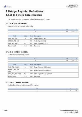
2.1.1 IRQ_STATUS (0x0000)Status of individual Interrupts in the bridge
31:6 5:2 1 0
R PWI MI SI
Field Bit(s) Mode Description
FAIL_IRQ (SI) 0 RO Target Timeout IRQ
MSPEC_IRQ (MI) 1 RO Model Specific IRQ
DMA_IRQ (PWI) 5:2 RO DMA Engine IRQ (0:3)
Reserved (R) 31:6 RO Reserved
2.1.2 IRQ_ENABLE (0x0004)Enables individual Interrupt sources
31:6 5:2 1 0
R PWI MI TI
Field Bit(s) Mode Description
FAIL_IRQ_EN (TI) 0 R/W Target Timeout IRQ Enable
MSPEC_IRQ_EN(MI) 1 R/W Model Specific IRQ Enable
DMA_IRQ_EN (PWI) 5:2 R/W DMA Engine IRQ (0:3) Enable
Reserved (R) 31:6 R/W Reserved
2.1.3 DMA_ENABLE (0x0008)Enables Direct Master and individual DMA engines
31:5 4:1 0
R DE ME
Page 4 Bridge Register Definitionsad-ug-0040_v1_1.pdf

ADMPCIE7V3PCIE Target Bridge
Field Bit(s) Mode Description
DMASTER_EN (ME) 0 R/W Direct Master (FPGA to PCIe) Enable
DMA_EN (DE) 4:1 R/W DMA Engine IRQ (0:3) Enable
Reserved (R) 31:5 R/W Reserved
2.1.4 FEATURES (0x000C)Core Features Register
31:5 4 3:0
R DDO MSLC
Field Bit(s) Mode Description
MSI_LEG_COMPAT(MSLC) 3:0 RO If not 0 MSI mode behaves in a way software compatible with Legacy
mode.
DMA_DESC_OVLP(DDO) 4 RO If 1
Reserved (R) 31:5 RO Reserved
2.1.5 PCIE_ERRS (0x0010)Count of correctable PCIe errors detected between the host and bridge causing GTX loss of sync.
31:16 15:0
R ERR
Field Bit(s) Mode Description
PCIE_ERRS (ERR) 15:0 RO Number of times PCIe has dropped out of L0 state since last PCIe reset
Reserved (R) 31:16 RO Reserved
2.1.6 PCIE_CTRL (0x0014) inital Value = 0xA5100100Configure PCIe active read requests in flight. DPIF is the maximum number of read requests any inidividualDMA engine can be waiting on.
31:28 27:24 23:22 21:12 11:10 9:0
TRIF DPIF R RPS R TPS
Page 5Bridge Register Definitionsad-ug-0040_v1_1.pdf

ADMPCIE7V3PCIE Target Bridge
Field Bit(s) Mode Init Value Description
Unused (TPS) 9:0 R/W 0x100 Not Implemented
Reserved (R) 11:10 R/W 00 Reserved
Unused (RPS) 21:12 R/W 0x100 Not Implemented
Reserved (R) 23:22 R/W 00 Reserved
RX_DMA_REQ_INFLIGHT (DPIF) 27:24 R/W 0x5 PCIe RX Packets in Flight limit for each DMA Engine
RX_TOT_REQ_INFLIGHT (TRIF) 31:28 R/W 0xa Not Implemented
2.1.7 PCIE_STATUS (0x0018)Status of PCIe link.
31 30 29:27 26:22 21:19 18 17 16 15:13 12:5 4:0
R LU LS LW MPS ET IE BM MRRS CBN CDN
Field Bit(s) Mode Description
CFG_DEVICE_NO(CDN) 4:0 RO Not Implemented
CFG_BUS_NO(CBN) 12:5 RO Not Implemented
MAX_RDREQ_SIZE(MRRS) 15:13 RO PCIe maximum read request size
BUS_MASTER (BM) 16 RO Not Implemented
INT_EN_N (IE) 17 RO Not Implemented
EXT_TAG (ET) 18 RO Not Implemented
MAX_PYLD_SIZE(MPS) 21:19 RO
PCIe Maximum payload sizeSize000 - 128Bytes001 - 256Bytes010 - 512Bytes011 - 1024Bytes100 - 2048Bytes101 - 4096Bytes11X - Reserved
ACT_LNK_WDTH(LW) 26:22 RO PCIe Configured link width
LINK_SPD (LS) 29:27 RO
PCIe link speed001 - Gen 1(2.5GBaud)010 - Gen 2(5GBaud)100 - Gen 3(8GBaud)
LINK_UP_N (LU) 30 RO PCIe link has configured and is active (inverted)
Reserved (R) 31 RO Reserved
Page 6 Bridge Register Definitionsad-ug-0040_v1_1.pdf

ADMPCIE7V3PCIE Target Bridge
2.1.8 FPGA_MASK (0x001C) inital Value = 0x003FFFFFControls the BAR2/3 or BAR4/5 address access, and can be modified to support PCI windows >4MB. Thisrequires custom bridge firmware, modified to request from BIOS at boot time, BAR2/3 greater than 4MB. Bydefault, systems are limited to occupying 4MB of PCIe space and this register cannot affect that.
31:29 28:22 21:0
ST0 CBN ST1
Field Bit(s) Mode Init Value Description
SET_TO_1 (ST1) 21:0 RO 0x3fffff ALWAYS 1s
SELECT_SIZE(CBN) 28:22 R/W 0x0 Selects between 4MB and 512MB address range
SET_TO_0 (ST0) 31:29 RO 000 ALWAYS 0s
2.1.9 FPGA_PAGEL (0x0020) inital Value = 0x00000000This registers allow OCP addresses outside the (4MB) PCI window to be accessed in the target FPGA, bysetting the upper address bits.
31:29 28:22 21:0
PL PM UNU
Field Bit(s) Mode Init Value Description
UNUSED (UNU) 21:0 R/W 0x0 Not Used
PAGE_MASKED(PM) 28:22 R/W 0x0 Sets OCP address bits 28:22 in Direct Slave Channel
PAGEL (PL) 31:29 R/W 000 Sets OCP address bits 31:29 in Direct Slave Channel
2.1.10 FPGA_PAGEH (0x0024) inital Value = 0x00000000This registers allow OCP addresses outside the (4MB) PCI window to be accessed in the target FPGA.
31:0
PH
Field Bit(s) Mode Init Value Description
PAGEH (PH) 31:0 R/W 0x0 Sets OCP address bits 63:32 in Direct Slave Channel
2.1.11 PCIE_BRG_STATUS (0x0034)Status flags from the PCIe Bridge Interface. Write anything to register to clear all Target FPGA Read Timeout orDMA Timeouts. Note that the target will remain inaccessible until the timeout bits are cleared, even if the TargetFPGA is reconfigured. Target Direct Master will not re-enable until register is cleared.
Page 7Bridge Register Definitionsad-ug-0040_v1_1.pdf

ADMPCIE7V3PCIE Target Bridge
31:28 27 26:24 23 22 21 20 19 18 17 16:13 12:8 7:5 4:0
R DME TO DT3 DT2 DT1 DT0 DMT B2TO LU BNF CNF TSM TTA
Field Bit(s) Mode Description
TX_TAGS_ACT(TTA) 4:0 RO Not Implemented
TX_FSM (TSM) 7:5 RO Not Implemented
RXCLPD_NF (CNF) 12:8 RO Not Implemented
RXBAR_NF (BNF) 16:13 RO Not Implemented
LINK_UP_N (LU) 17 RO Not Implemented
BAR2TO (B2TO) 18 RO PCIe Read request has timed out on BAR2
DMTIMEOUT (DMT) 19 RO DMA PCIe Read request has timeout out on Direct Master
DMATIMEOUT0(DT0) 20 RO DMA PCIe Read request has timeout out on DMA Channel 0
DMATIMEOUT1(DT1) 21 RO DMA PCIe Read request has timeout out on DMA Channel 1
DMATIMEOUT2(DT2) 22 RO DMA PCIe Read request has timeout out on DMA Channel 2
DMATIMEOUT3(DT3) 23 RO DMA PCIe Read request has timeout out on DMA Channel 3
TIMEOUT (TO) 26:24 RO Not Implemented
DM ERROR (DME) 27 RO Illegal Direct Master Command detected from Target
Reserved (R) 31:28 RO Reserved
Page 8 Bridge Register Definitionsad-ug-0040_v1_1.pdf

ADMPCIE7V3PCIE Target Bridge
2.2 ADB3 Generic DMA Register Mapping
The following register mapping is used for each DMA engine in the Generic Bridge Block. DMA engines areoffset from the Base Address of BAR 0 at 64 byte intervals. DMA engine #0 starts at address 0x0040, DMAengine #1 at 0x0080 etc.
2.2.1 ABORT/STATUS (0x0040)When written to, this register aborts any current DMA transfers, the DMA engine FSMs will however remain in theabort state to allow inflight PCIe/MPTL reads to complete.
31:28 27:26 25:23 22:20 19:18 17:16 15 14 13:12 11:9 8:6 5:4 3:2 1 0
FF R MRA PRA MWA PWA MA PA R MRI PRI MWI PWI MI PI
Field Bit(s) Mode Description
PCIe Fetch Idle (PI) 0 RO Descriptor Fetch (PCIe side) Idle
MPTL Fetch Idle (MI) 1 RO Descriptor Fetch (MPTL side) Idle
PCIE Write WorkerIdle (PWI) 3:2 RO PCIe Side Write Worker Idle
MPTL Write WorkerIdle (MWI) 5:4 RO MPTL Side Write Worker Idle
PCIE Read WorkerIdle (PRI) 8:6 RO PCIe Side Read Worker Idle
MPTL Read WorkerIdle (MRI) 11:9 RO MPTL Side Read Worker Idle
Reserved (R) 13:12 RO Reserved
PCIe DescriptorFetch Abort (PA) 14 RO Descriptor Fetch (PCIe side) Aborting
MPTL DescriptorFetch Abort (MA) 15 RO Descriptor Fetch (MPTL side) Aborting
PCIe Write WorkerFetch Abort (PWA) 17:16 RO PCIe Side Write Worker Aborting
MPTL Write WorkerFetch Abort (MWA) 19:18 RO MPTL Side Write Worker Aborting
PCIe Read WorkerFetch Abort (PRA) 22:20 RO PCIe Side Read Worker Aborting
MPTL Read WorkerFetch Abort (MRA) 25:23 RO MPTL Side Read Worker Aborting
Reserved (R) 27:26 RO Reserved
FSM Fail (FF) 31:28 RO FSM Fail Bits
Page 9Bridge Register Definitionsad-ug-0040_v1_1.pdf
ADMPCIE7V3PCIE Target Bridge
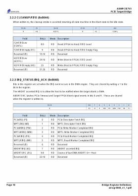
2.2.2 CLEANUP/FIFO (0x0044)When written to, the cleanup strobe is asserted returning all state machine in the Abort state to the Idle state.
31:26 25 24:16 15:10 9 8:0
R HE H2FFL R FE F2HFL
Field Bit(s) Mode Description
F2HFIFOLev(F2HFL) 8:0 RO Read (FPGA to Host) FIFO Level
F2HFIFOEmpty (FE) 9 RO Read (FPGA to Host) FIFO Empty Flag
Reserved (R) 15:10 RO Reserved
H2FFIFOLev(H2FFL) 24:16 RO Write (Host to FPGA) FIFO Level
H2FFIFOEmpty (HE) 25 RO Write (Host to FPGA) FIFO Empty Flag
Reserved (R) 31:26 RO Reserved
2.2.3 IRQ_STATUS/IRQ_ACK (0x0048)Bits in this register are set when the IRQ event occurs in the DMA engine. They are cleared by writing a 1 to thebit in the register.
The ABORT asserted IRQ is to allow the host to be notified when the target aborts a DMA.
ABORTSRC latches PCIe Timeout and Target FPGA Abort signal events in bits 8 and 9. These are clearedwhen the register is written to.
33:10 9:8 7 6 5 4 3 2 1 0
R AS AI R MR PR MW PW MI PI
Field Bit(s) Mode Description
PCIeIRQ (PI) 0 RO PCIe Descriptor Fetch IRQ
MPTLIRQ (MI) 1 RO MPTL Descriptor Fetch IRQ
PCIeWIRQ (PW) 2 RO PCIe Write Worker Completed IRQ
MPTLWIRQ (MW) 3 RO MPTL Write Worker Completed IRQ
PCIeRIRQ (PR) 4 RO PCIe Read Worker Completed IRQ
MPTLRIRQ (MR) 5 RO MPTL Read Worker Completed IRQ
Reserved (R) 6 RO Reserved
ABORTIRQ (AI) 7 RO ABORT asserted IRQ
ABORTSRC (AS) 9:8 RO Source of last DMA ABORT: 0=> Host
Reserved (R) 33:10 RO Reserved
Page 10 Bridge Register Definitionsad-ug-0040_v1_1.pdf

ADMPCIE7V3PCIE Target Bridge
2.2.4 IRQ_ENABLE (0x004C)This register enables the interrupt bits in the IRQ_STATUS register, and allows then to interrupt the host.
31:8 7 6 5 4 3 2 1 0
R AI R MR PR MW PW MI PI
Field Bit(s) Mode Description
PCIeIRQ_EN (PI) 0 RO PCIe Descriptor Fetch IRQ Enable
MPTLIRQ_EN (MI) 1 RO MPTL Descriptor Fetch IRQ Enable
PCIeWIRQ_EN (PW) 2 RO PCIe Write Worker Completed IRQ Enable
MPTLWIRQ_EN(MW) 3 RO MPTL Write Worker Completed IRQ Enable
PCIeRIRQ_EN (PR) 4 RO PCIe Read Worker Completed IRQ Enable
MPTLRIRQ_EN (MR) 5 RO MPTL Read Worker Completed IRQ Enable
Reserved (R) 6 RO Reserved
ABORTIRQ_EN (AI) 7 RO ABORT IRQ Enable
Reserved (R) 31:8 RO Reserved
2.2.5 NDL/NDH (0x0050-0x0054)This register should be set with the first descriptor in a chain for the PCIe or MPTL Descriptor Fetch Engine toread. The descriptors can be in either host PCIe space or in the target, but they all described host PCIeaddresses.
31:0
NDL/NDH
Field Bit(s) Mode Description
NDL/NDH (NDL/NDH) 31:0 RO NDL - Next Descriptor Low (0x10)|NDH - Next Descriptor High(0x14)
2.2.6 HOST_CTL (0x0058)PCIe Packet Size Limits and Descriptor source select control
31:19 18 17:10 9:0
R DS R MPRS
Field Bit(s) Mode Description
MAXPCIeREQSIZE(MPRS) 9:0 R/W Maximum PCIe Read Request Size
Reserved (R) 17:10 RO Reserved
Page 11Bridge Register Definitionsad-ug-0040_v1_1.pdf

ADMPCIE7V3PCIE Target Bridge
Field Bit(s) Mode Description
DFESEL (DS) 18 R/WDescriptor Fetch Engine Select:0 - PCIe1 - MPTL
Reserved (R) 31:19 RO Reserved
2.2.7 FPGA_CTL (0x005C)Controls size of MPTL transfers
31:26 25:16 15:10 9:0
R MMRS R MMWS
Field Bit(s) Mode Description
MAXMPTLWREQSIZE(MMWS) 9:0 R/W Maximum MPTL Write Request/Burst Size
Reserved (R) 15:10 RO Reserved
MAXMPTLRREQSIZE(MMRS) 25:16 R/W Maximum MPTL Read Request/Burst Size
Reserved (R) 31:26 RO Reserved
2.2.8 Reserved (0x0060)These registers control the maximum burst size of MPTL read and write commands generated by the DMAengines. It should be noted that to avoid potential overflows, larger burst sizes will result in lower limit for readrequests in flight. Only powers of 2 should be specified. Also to avoid potential overflows, the total burst sizespread across all DMA engines in use should be 32/(number of active DMA engines).
2.2.9 DF_WAIT/ILLEGAL (0x0064)Writing to this register allows a Descriptor Fetch Engine (paused by its descriptor flags) to continue and fetch itsnext descriptor.
31 30:2 1 0
IW R MW PW
Field Bit(s) Mode Description
PCIeWHW (PW) 0 RO PCIe Descriptor Fetch Engine waiting on Host Write
MPTLWHW (MW) 1 RO MPTL Descriptor Fetch Engine waiting on Host (or MPTL Direct Master)Write
Reserved (R) 30:2 RO Reserved
ILLREGW (IW) 31 RO Illegal Register write
2.3 ADMPCIE7V3 Control Registers (BAR1)
Page 12 Bridge Register Definitionsad-ug-0040_v1_1.pdf

ADMPCIE7V3PCIE Target Bridge
2.3.1 Reserved (0x0000)
2.3.2 Reserved (0x0004)
2.3.3 DATE (0x0008)Unique Version Identifier Code. Date of core build in format 0xDDMMYYYY. This identifies the creation date ofthe bridge, combined with the bridge time stamp register, this uniquely identifies the bridge version.
31:24 23:16 15:0
DY MO YR
Field Bit(s) Mode Description
YEAR (YR) 15:0 RO .
MONTH (MO) 23:16 RO .
DAY (DY) 31:24 RO .
2.3.4 TIME (0x000C)Unique Version Identifier Code. Time of core build in format 0xHHMMSS00. This identifies the creation time ofthe bridge, combined with the bridge date stamp register, this uniquely identifies the bridge version.
31:24 23:16 15:8 7:0
HO MI SE UN
Field Bit(s) Mode Description
Unused (UN) 7:0 RO Zeros
SECONDS (SE) 15:8 RO .
MINUTES (MI) 23:16 RO .
HOUR (HO) 31:24 RO .
2.3.5 Reserved (0x0010)
2.3.6 Reserved (0x0014)
2.3.7 Reserved (0x0018)
2.3.8 Reserved (0x001C)
Page 13Bridge Register Definitionsad-ug-0040_v1_1.pdf

ADMPCIE7V3PCIE Target Bridge
2.3.9 Reserved (0x0020)
2.3.10 Reserved (0x0024)
2.3.11 Reserved (0x0028)
2.3.12 Reserved (0x002C)
2.3.13 ICTL (0x0030) inital Value = 0x0X00000400Interrupt Control Register
This register allows the FPGA and System Monitor interrupts to be enabled / disabled.
31:9 8 7:1 0
RES FL0 RES FE
Field Bit(s) Mode Init Value Description
FP_ENABLE (FE) 0 RW 0 0 => FPGA interrupt is disabled1 => FPGA interrupt is enabled
Reserved (RES) 7:1 MBZ 0x0 .
FP0_LEVEL (FL0) 8 RW 0 0 => FPGA 0 interrupt is negative edge sensitive1 => FPGA 0 interrupt is active-low level-sensitive
Reserved (RES) 31:9 MBZ 0x2 .
2.3.14 ISTAT (0x0034) inital Value = 0x0X00000000Interrupt Status Register
This register can be read to determine whether an FPGA or System Monitor interrupt is pending and permits thehost to clear the interrupts.
31:1 0
RES FI
Field Bit(s) Mode Init Value Description
FPINT (FI) 0 RW1C 0
When read:
0 => FPGA interrupt is not pending1 => FPGA interrupt is pending
If ICTL.FP_LEVEL = 0
Reserved (RES) 31:1 MBZ 0x0 .
Page 14 Bridge Register Definitionsad-ug-0040_v1_1.pdf

ADMPCIE7V3PCIE Target Bridge
2.3.15 Reserved (0x0038)
2.3.16 Reserved (0x003C)
2.3.17 FLCTL (0x0040) inital Value = 0x0X00000000Flash Control Register
31 30 29 28 27 26 25 24 23 22:21 20 19:17 16:1 0
RT WE OE S ER EC EA ED MR RES B RES AD R
Field Bit(s) Mode Init Value Description
Reserved (R) 0 MBZ 0 .
ADDR (AD) 16:1 RW 0x0 Page offset address to be output to Flash memory.When read
Reserved (RES) 19:17 MBZ 000 .
BUSY (B) 20 RO 0 Returns the actual value on FL_WAIT pin
Reserved (RES) 22:21 MBZ 00 .
MVMRO (MR) 23 RO 0 0 => writes to Flash are enabled1 => writes to Flash are disabled in h/w
EN_DATA (ED) 24 RW 0 0 => do not drive Flash data bus
EN_ADDR (EA) 25 RW 0 0 => do not drive Flash address bus
EN_CTL (EC) 26 RW 0 0 => do not drive flash control lines FL_CEL
EN_RST (ER) 27 RW 0 0 => do not drive FL_RSTL1 => drive FL_RSTL
SEL (S) 28 RW 0
When written:0 = > do not assert FL_CEL pin1 => assert FL_CEL pin.When read
OE (OE) 29 RW 0
When written:0 = > do not assert FL_OEL pin1 => assert FL_OEL pin.When read
WE (WE) 30 RW 0
When written:0 = > do not assert FL_WEL pin1 => assert FL_WEL pin.When read
RST (RT) 31 RW 0When written:0 = > do not assert FL_RSTL pin1 => assert FL_RSTL pin
Page 15Bridge Register Definitionsad-ug-0040_v1_1.pdf
ADMPCIE7V3PCIE Target Bridge
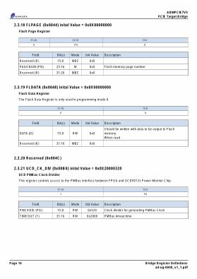
2.3.18 FLPAGE (0x0044) inital Value = 0x0X00000000Flash Page Register
31:26 25:16 15:0
R PN R
Field Bit(s) Mode Init Value Description
Reserved (R) 15:0 MBZ 0x0 .
PAGENUM (PN) 25:16 M 0x0 Flash memory page number
Reserved (R) 31:26 MBZ 0x0 .
2.3.19 FLDATA (0x0048) inital Value = 0x0X00000000Flash Data Register
The Flash Data Register is only used in programming mode 0.
31:16 15:0
R D
Field Bit(s) Mode Init Value Description
DATA (D) 15:0 RW 0x0Should be written with data to be output to Flashmemory.When read
Reserved (R) 31:16 MBZ 0x0 .
2.3.20 Reserved (0x004C)
2.3.21 UCD_CK_DIV (0x00B0) inital Value = 0x0X20000320UCD PMBus Clock Divider
This register controls access to the PMBus interface between FPGA and UCD9012x Power Monitor Chip.
31:16 15:0
T PD
Field Bit(s) Mode Init Value Description
PMCKDIV (PD) 15:0 RW 0x320 Clock divider for generating PMBus Clock
TIMEOUT (T) 31:16 RW 0x2000 PMBus timout time
Page 16 Bridge Register Definitionsad-ug-0040_v1_1.pdf

ADMPCIE7V3PCIE Target Bridge
2.3.22 UCD_CTRL (0x00B4) inital Value = 0x0X00000000UCD PMBus Control Register
This register controls access to the PMBus interface between FPGA and UCD9012x Power Monitor Chip. Theuser mode bit must be set to allow host access to PMBus and disable automatic sensor reading.
31:30 29:23 22:16 15 14 13 12 11 10 9 8 7:0
CL R ADDR UM F H B IM R WT RT RWL
Field Bit(s) Mode Init Value Description
RWLEN (RWL) 7:0 RW 0x0 Number of bytes to read from or write to PMBus
RD_TRIG (RT) 8 RW 0 Write 1 to trigger PMBus Read Command
WR_TRIG (WT) 9 RW 0 Write 1 to trigger PMBus Write Command
Reserved (R) 10 MBZ 0 .
I2C_MODE (IM) 11 RW 0 0 => SMBus command protocol
BUSY (B) 12 RO 0 PMBus Command Busy
HOLD (H) 13 RO 0 PMBus Holding Data
FAULT (F) 14 RO 0 PMBus Fault Detected
USER_MODE (UM) 15 RW 0 Write 1 to request User Mode access
ADDR (ADDR) 22:16 RW 0x0 UCD9012x bus address : 0x4E
Reserved (R) 29:23 MBZ 0x0 .
CMNDLEN (CL) 31:30 RW 00 Length of PMBus Command written before read or eritrof data
2.3.23 UCD_CMND (0x00B8) inital Value = 0x0X00000000UCD PMBus Command Register
This register sets the command and data sent and raed from the PMBus interface.
31:24 23:16 15:0
RD WD C
Field Bit(s) Mode Init Value Description
CMND (C) 15:0 RW 0x0 Command to send to PMBus
WDATA (WD) 23:16 RW 0x0 Data to send to PMBus
RDATA (RD) 31:24 RO 0x0 Last data byte read from PMBus
Page 17Bridge Register Definitionsad-ug-0040_v1_1.pdf

ADMPCIE7V3PCIE Target Bridge
2.3.24 UCD_RDBUF (0x00BC) inital Value = 0x0X00000000UCD PMBus Command Read Buffer
This allows multiple byte read commands (up to 4 bytes) to be read back by the host.
31:0
D
Field Bit(s) Mode Init Value Description
DATA (D) 31:0 RO 0x0 Last 4 bytes received from PMBus
2.3.25 IIC_CTL (0x0400) inital Value = 0x0X00000000IIC Control Register
This register controls the two I2C interfaces. It has two modes of operation:
A "discrete" command will perform a single read or write operation on the interface.
A "block read" command will copy data from an I2C device to block RAM in the bridge.
Block reads from the VPD ID PROM will copy 256 bytes from the PROM to the REG VPDBUF.
All other block reads will copy 256 bytes from the selected device to the REG IICBUF.
NOTES:
(1) The I2C interface does not auto-detect activity on the bus.
31:30 29 28 27 26:25 24 23 22:16 15:8 7:0
R IA1 E RD M W IA0 CHAD ADDR DATA
Field Bit(s) Mode Init Value Description
DATA (DATA) 7:0 RW 0x0
Write:8 Bit data value for discrete writes
Read:If READY = 1 and WRITE = 0
ADDR (ADDR) 15:8 RW 0x0
Discrete Commands:Address
Shadow Read or Memory Copy:unused
CHIP_ADR (CHAD) 22:16 M 0x0 Serial Bus Chip Address
IF_ADR0 (IA0) 23 M 0
Bit 0 of IF Select00 => I2C Interface 2 (SI5338)01 => I2C Interface 4 (VPD)10 => I2C Interface 5 (SODIMM)
WRITE (W) 24 RW 0 ???
Page 18 Bridge Register Definitionsad-ug-0040_v1_1.pdf

ADMPCIE7V3PCIE Target Bridge
Field Bit(s) Mode Init Value Description
MODE (M) 26:25 Wm 00
00 => NOP01 => Discrete Command10 => Block Read11 => reserved
READY (RD) 27 RO 0 Returns a 1 if the interface is ready to accept a newcommand.
ERROR (E) 28 RWC 0 Signifies an error in the transfer. The flag is reset whena '1' is written to this bit.
IF_ADR1 (IA1) 29 M 0
Bit 1 of IF Select00 => I2C Interface 2 (SI5338)01 => I2C Interface 4 (VPD)10 => I2C Interface 5 (SODIMM)
Reserved (R) 31:30 MBZ 00 .
2.3.26 IIC_STAT (0x0404) inital Value = 0x0X00000000IIC Status Register
31:0
TBD
Field Bit(s) Mode Init Value Description
TBD (TBD) 31:0 RO 0x0 TBD
2.3.27 VPDBUF (0x0600-0x06FC) inital Value = 0x0X00000000VPD Shadow Buffer
The contents of the VPD ROM are copied to this buffer at power-up. Refer to the ADM-PCIE-7V3 VPDSpecification for details.
31:24 23:16 15:8 7:0
D3 D2 D1 D0
Field Bit(s) Mode Init Value Description
DATA0 (D0) 7:0 M 0x0 Shadow of the Data at Adr+0
DATA1 (D1) 15:8 M 0x0 Shadow of the Data at Adr+1
DATA2 (D2) 23:16 M 0x0 Shadow of the Data at Adr+2
DATA3 (D3) 31:24 M 0x0 Shadow of the Data at Adr+3
Page 19Bridge Register Definitionsad-ug-0040_v1_1.pdf

ADMPCIE7V3PCIE Target Bridge
2.3.28 IICBUF (0x0700-0x07FC) inital Value = 0x0X00000000IIC Monitor Shadow Buffer
A MemCopy command to the REG IIC_CTL register will result in the contents of the addressed device beingcopied to this buffer.
31:24 23:16 15:8 7:0
D3 D2 D1 D0
Field Bit(s) Mode Init Value Description
DATA0 (D0) 7:0 M 0x0 Shadow of the Data at Adr+0
DATA1 (D1) 15:8 M 0x0 Shadow of the Data at Adr+1
DATA2 (D2) 23:16 M 0x0 Shadow of the Data at Adr+2
DATA3 (D3) 31:24 M 0x0 Shadow of the Data at Adr+3
2.3.29 UCD90120_BUF (0x0A00-0x0AFC)UCD90120 Rail Buffer
This buffer contains the Voltage, Current and Temperature readings from the UCD90120 rails. Each railoccupies 16 bytes of buffer space.
111:107 106:96 79:75 74:64 47:32 4:0
TE T IE I V VE
Field Bit(s) Mode Description
VMODE (VE) 4:0 M 5 bit signed exponent of Rail Voltage
VOUT (V) 47:32 M 16 bit integer mantissa of Rail Voltage
IOUT (I) 74:64 M 11 bit integer mantissa of Rail Current
IEXP (IE) 79:75 M 5 bit signed exponent of Rail Current
TOUT (T) 106:96 M 11 bit integer mantissa of Chip Temperature
TEXP (TE) 111:107 M 5 bit signed exponent of Chip Temperature
3 DMA Engine OperationThis section describes the detailed operation of the DMA engine
Figure 3 shows the overall structure of the ADB3 DMA Engine.
Page 20 DMA Engine Operationad-ug-0040_v1_1.pdf

ADMPCIE7V3PCIE Target Bridge
FIFO
3 PortADB3-OCP
MUX
DescriptorFetch
Engine
WriteWorkerEngine ADB3
OCPMaster
ReadWorkerEngine
BYTERotate
FIFOBYTERotate
DescriptorFetch
Engine
ReadWorkerEngine
WriteWorkerEngine
3 PortADB3-OCP
MUXADB3OCPMaster
Configuration and Status Registers
PCIe (Host)Transfers
MPTL (FPGA)Transfers
Figure 3 : ADB3 DMA Engine
On the host side the basic operation is for a descriptor fetch engine to request descriptors from the host to getaddress, read/write, chunk size and other information. Each descriptor is then converted to a command that ispushed to either a read or write worker DMA engine on the PCIe side and a similar command is pushed to thecomplimentary worker DMA engine on the AXI4 side.
The read worker engine will generate read requests (sent to PCIe or AXI4) and push the returned data into theread FIFO through byte rotation logic. The byte rotation is set for the entire DMA transfer which may consist of along chain of descriptors. The descriptor fetch engine can switch the alignment within a chain, although it has toempty the FIFO and re-synchronise the read and write sides to do so. The write worker engines, will pull byterotated data from the FIFO and send it out as write requests to the PCIe end point.
Using the AXI4 Side Descriptor Fetch engine, to allow the Host Worker descriptors to be stored in the FPGArather than in Host memory is also possible.
3.1 Principal Sub-modulesThe main DMA operation is split between 3 types of DMA engines, the Descriptor Fetch engines, the ReadWorkers and the Write Workers. The FIFOs also have some byte rotation functionality. The commands aremultiplexed onto a single bus.
3.1.1 Descriptor Fetch Engine
This module performs the higher level DMA control for the host side of the DMA transfer. The state machine isstarted by writing a descriptor address to a 64 bit register. The fetch engine will fetch a descriptor using a Readfrom this address containing the following information:
• PCIE DMA chunk start address
Page 21DMA Engine Operationad-ug-0040_v1_1.pdf

ADMPCIE7V3PCIE Target Bridge
• DMA chunk length
• next descriptor address
• AXI4 DMA chunk start address
• read or write data
• if last descriptor in transfer
• if PCIE side worker to generate an IRQ on completion
• if AXI4 side worker to generate an IRQ on completion
• if fetch engine to generate IRQ immediately on reading descriptor
• if fetch engine is to wait on acknowledgment before sending command to worker
• if fetch engine must wait for write complete, flush FIFOs and re-align data before next descriptor
• AXI4 side chunk length modifier - can be used to align AXI4 side transfers to always finish on 16 byteboundary, and avoid double read/write effect.
The fetch engine will then generate an interrupt if the appropriate bit is set (this is to notify the host that it cansafely update the descriptor table.)
If the fetch engine is to wait on an acknowledgment then it will do so (this is to prevent the engine from readingany descriptors before the host has updated them - note that this bit need not be set in the same descriptor asthe IRQ generating descriptor.) Note that the wait acknowledgment bit is cleared separately from clearing theIRQ bit.
If the alignment needs to be set, either because this is the first descriptor, or because the previous PCIEdescriptor finished on an unaligned boundary, or because the previous descriptor had its flush bit set, then a newalignment value will be sent to the FIFOs based on the PCIE and AXI4 address LSBs. The PCIE address andtransfer length will be checked and if they do not finish on a 16 byte boundary, a flag will be set.
The read and write worker engines have command queues for the DMA chunks. If these are not full (should beempty at the start of DMA transfer - should not be possible to start fetch if not empty), the fetch engine can senda command to the worker containing the following information:
• DMA Chunk Start Address
• DMA Chunk length
• read or write (used to select worker for command)
• generate IRQ on completion
• last descriptor in chain (used to clean up byte rotation FIFO effect)
• fixed address (always 0 for PCIe side of transfer)
Once this command has been posted to the worker, if the PCIe transfer does not finish on a 32 byte boundary orthe flush bit is set then the descriptor engine will wait for the write side to finish. If neither of these cases is true(and therefore the FIFO alignment is the same for the next descriptor) the descriptor fetch engine can fetch andprocess the next descriptor in the chain.
The fetch engine will generate a read using the next descriptor address (unless the last descriptor is specified.)The fetch engine will fetch as many descriptors and push them into the workers input FIFO as the worker willallow.
3.1.2 Read Worker
The Read Worker is the main DMA engine for read transfers from the memory mapped addres space to theFIFO. This module is used on both the Host and FPGA side. On the FPGA side however its use is morerestricted, as start addresses must be 16 byte aligned.
Page 22 DMA Engine Operationad-ug-0040_v1_1.pdf

ADMPCIE7V3PCIE Target Bridge
This module has an input queue of commands, implemented using a 16 word deep synchronous FIFO, with anearly full flag used to indicate to any command source that it is not ready to accept data. On the Host side,possible command sources are the Host Descriptor Fetch Engine, the FPGA Descriptor Fetch Engine and directregister write. On the FPGA side, only direct register writes are possible.
The command contains the following information:
• DMA Chunk Start Address
• DMA Chunk length
• read or write ( must be read)
• generate IRQ on completion
• last descriptor in chain (used to clean up byte rotation FIFO effect)
• fixed address
The read worker consists of 3 state machines. The first state machine reads each Chunk Command, and breaksit into a succession of smaller burst transfers. This state machine aligns the first address to a 32 byte boundary ifnecessary (the extra data read here is removed by the byte rotation in the FIFO).
If the transfer length left is greater than the maximum burst size (programmed by a register) then burst sizes ofthis maximum burst size will be chosen, otherwise, shorter bursts matching the number of 32 byte wordsremaining will be used. The last burst will be extended if necessary to form a complete 32 byte boundary burst,with the extra data thrown away by the byte rotation FIFO.
This state machine only calculates addresses and burst sizes. These are pushed into a small FIFO and bufferedbefore being used by the read request state machine. If the command specifies the generation of an IRQ, thenthis state machine will push a generate IRQ command into the FIFO after the last read command.
The small FIFO is read by the read request state machine. This state machine reads commands out of the FIFOand dispatches read requests. It also uses 3 tag bits to tag the request order. The tag, burst size or an IRQ flagare pushed into another small FIFO to keep track of inflight requests. If the main DMA FIFO is getting too full, orthe inflight FIFO is nearly full this state machine will stall.
A third state machine is used to complete the read requests. This reads the inflight FIFO, and uses its burstlength and tag information to verify the Resp Data. Out of order data can be handled to an extent, with data withnon-matching tag pushed into a sidetrack FIFO. When the inflight request is read with the matching tag, data isread from the FIFO before further Responses are accepted. The received Response Data is pushed into themain DMA FIFO.
If a DMA Chunk Length of 0 is specified, the worker DMA will go into continuous mode, which will continuallyread data until the abort signal is asserted.
3.1.3 Write Worker
The Write Worker is the main DMA engine for write transfers from memory mapped address space to the FIFO.This module is used on both the Host and FPGA side. On the FPGA side however its use is more restricted, asstart addresses must be 32 byte aligned.
This module has an input queue of commands, implemented using a 32 word deep synchronous FIFO, with anearly full flag used to indicate to any command source that it is not ready to accept data. On the Host side,possible command sources are the Host Descriptor Fetch Engine, the FPGA Descriptor Fetch Engine and directregister write. On the FPGA side, only direct register writes are possible.
The command contains the following information:
• DMA Chunk Start Address
Page 23DMA Engine Operationad-ug-0040_v1_1.pdf

ADMPCIE7V3PCIE Target Bridge
• DMA Chunk length
• read or write ( must be write)
• generate IRQ on completion
• last descriptor in chain (used to clean up byte rotation FIFO effect)
• fixed address
The read worker consists of 2 state machines. The first state machine reads each Chunk Command, and breaksit into a succession of smaller burst transfers. If the first address is not 32 byte aligned, this state machinegenerates an initial short 1-beat write with byte enables. The data is least significant bit aligned and is read outunaligned from the main DMA FIFO. (note that this first transfer will not occur on the FPGA side). Successivewrite bursts will then be 32 byte aligned.
If the transfer length left is greater than the maximum burst size (programmed by a register) then burst sizes ofthis maximum burst size will be chosen, otherwise, a shorter burst matching the number of 16 byte wordsremaining will be used. If there are still bytes left to transfer, a short 1-beat write using byte enables will be usedto complete the transaction. All these transactions after the first use the byte aligned FIFO output.
This state machine only calculates addresses and burst sizes. These are pushed into a small FIFO and bufferedbefore being used by the write state machine. If the command specifies the generation of an IRQ, then this statemachine will push a generate IRQ command into the FIFO after the last read command. If the commandspecifies the last descriptor in a transaction, then this state machine will push a last_descriptor command into theFIFO after the last write burst specification.
The small FIFO is read by the write state machine. This state machine reads commands out of the FIFO anddispatches write requests. It reads data from the main DMA FIFO (byte aligned or not depending on whether itsan initial unaligned transfer or not), and pushes it out as Data, Byte Enables and Data Valid signals.
This state machine will generate an IRQ on completion if specified in the descriptor. If the last descriptor isspecified, the extra word in unaligned transfers will be flushed from the main FIFO.
If a DMA Chunk Length of 0 is specified, the worker DMA will go into continuous mode, which will continuallywrite data until the abort signal is asserted.
3.1.4 Alignment Write FIFO
This is simply a generic 256 bit wide FIFO with 2x256 bit registers at the input side.
3.1.5 Alignment Read FIFO
This is a 256 bit wide FIFO with an extra 2x256 bit registers at its input to provide byte shifting. The byte rotationvalue must be written in with a write enable before each DMA to ensure proper alignment, and clear possibleeffects due to the last DMA.
3.1.6 3-Port MUX
These MUX modules provide simplified 3 port MUX access for the 3 memory mapped masters. They aresimplified based on the knowledge that only 1 port writes, and 2 ports only read. It modifies the tags on the readrequests, to differentiate between DMA data and Descriptors.
3.1.7 Abort and Cleanup Signals
None of the modules have global reset. To escape from an error situation, 2 signals are provided: Abort andCleanup. Abort is used to send all the state machines into a safe recovery state if necessary. In this state, thestate machines will generate no new transactions but will accept completions from transactions elsewhere in thesystem. The state machine will also flush all FIFOs in the module. After a length of time, the cleanup signal canbe asserted to return the state machines to the idle state.
Page 24 DMA Engine Operationad-ug-0040_v1_1.pdf

ADMPCIE7V3PCIE Target Bridge
3.1.8 DMA Descriptor Definition
The DMA descriptor is a 256 bit word with the following information:
. pcie_start_addr := (63 downto 0);
. xfer_length := (89 downto 64);
. next_descriptor := (191 downto 128);
. local_start_addr := (231 downto 192);
. read_data := (240); (FPGA to Host)
. last_descriptor := (241);
. irq_on_pcie_completion := (242);
. irq_on_mptl_completion := (243);
. irq_now := (244);
. wait_irq_ack := (245);
. mptl_address_fixed := (246);
. flush_data := (247);
. local_length_adjustment := (252 downto 248);
3.1.9 Control and Status Register Fields
The control and status registers and write strobes are defined in the following record types:
type adb3 dma control register type is record -- Abort and Cleanup Strobes abort : std logic; cleanup : std logic; -- Descriptor Fetch Address and WE/Start Strobe descriptor host addr : std logic vector(63 downto 0); descriptor host we : std logic; -- Descriptor Fetch from FPGA with WE/Start Strobe -- (descriptors for Host Side addresses though) descriptor fpga addr : std logic vector(63 downto 0); descriptor fpga we : std logic; -- Maximum Burst Sizes for DMA Engines host write worker max burst : std logic vector(9 downto 0); host read worker max burst : std logic vector(9 downto 0); fpga write worker max burst : std logic vector(9 downto 0); fpga read worker max burst : std logic vector(9 downto 0); -- IRQ Acknowledge irq ack register : std logic vector(6 downto 0); irq ack we : std logic; descriptor fpga wait ack : std logic;end record; type adb3 dma status register type is record fsm idle : std logic vector(13 downto 0); fsm aborting : std logic vector(13 downto 0); fsm fail : std logic vector(3 downto 0); illegal we : std logic; irq status : std logic vector(6 downto 0); fifo info : std logic vector(31 downto 0);end record;
Page 25DMA Engine Operationad-ug-0040_v1_1.pdf

ADMPCIE7V3PCIE Target Bridge
3.2 Register Memory MapsBase registers for Bridge control/status.
3.2.1 ADB3 Generic Bridge Control Registers
Register Address Description
IRQ_STATUS 0x0000 Status of individual Interrupts in the bridge
IRQ_ENABLE 0x0004 Enables individual Interrupt sources
DMA_ENABLE 0x0008 Enables Direct Master and individual DMA engines
FEATURES 0x000C Core Features Register
PCIE_ERRS 0x0010 Count of correctable PCIe errors detected between the host andbridge causing GTX loss of sync.
PCIE_CTRL 0x0014Configure PCIe active read requests in flight. DPIF is the maximumnumber of read requests any inidividual DMA engine can be waitingon.
PCIE_STATUS 0x0018 Status of PCIe link.
FPGA_MASK 0x001C
Controls the BAR2/3 or BAR4/5 address access, and can be modifiedto support PCI windows >4MB. This requires custom bridge firmware,modified to request from BIOS at boot time, BAR2/3 greater than4MB. By default, systems are limited to occupying 4MB of PCIe spaceand this register cannot affect that.
FPGA_PAGEL 0x0020 This registers allow OCP addresses outside the (4MB) PCI window tobe accessed in the target FPGA, by setting the upper address bits.
FPGA_PAGEH 0x0024 This registers allow OCP addresses outside the (4MB) PCI window tobe accessed in the target FPGA.
PCIE_BRG_STATUS 0x0034
Status flags from the PCIe Bridge Interface. Write anything to registerto clear all Target FPGA Read Timeout or DMA Timeouts. Note thatthe target will remain inaccessible until the timeout bits are cleared,even if the Target FPGA is reconfigured. Target Direct Master will notre-enable until register is cleared.
DMA engine registers, DMA0 registers start at offset 0x040 and DMA1 from 0x080
3.2.2 Generic DMA Register Mapping
Register Address Description
ABORT/STATUS 0x0040When written to, this register aborts any current DMA transfers, theDMA engine FSMs will however remain in the abort state to allowinflight PCIe/MPTL reads to complete.
CLEANUP/FIFO 0x0044 When written to, the cleanup strobe is asserted returning all statemachine in the Abort state to the Idle state.
Page 26 DMA Engine Operationad-ug-0040_v1_1.pdf

ADMPCIE7V3PCIE Target Bridge
Register Address Description
IRQ_STATUS/IRQ_ACK 0x0048
Bits in this register are set when the IRQ event occurs in the DMAengine. They are cleared by writing a 1 to the bit in the register.The ABORT asserted IRQ is to allow the host to be notified when thetarget aborts a DMA.ABORTSRC latches PCIe Timeout and Target FPGA Abort signalevents in bits 8 and 9. These are cleared when the register is writtento.
IRQ_ENABLE 0x004C This register enables the interrupt bits in the IRQ_STATUS register,and allows then to interrupt the host.
NDL/NDH0x0050
-0x0054
This register should be set with the first descriptor in a chain for thePCIe or MPTL Descriptor Fetch Engine to read. The descriptors canbe in either host PCIe space or in the target, but they all describedhost PCIe addresses.
HOST_CTL 0x0058 PCIe Packet Size Limits and Descriptor source select control
FPGA_CTL 0x005C Controls size of MPTL transfers
Reserved 0x0060
These registers control the maximum burst size of MPTL read andwrite commands generated by the DMA engines. It should be notedthat to avoid potential overflows, larger burst sizes will result in lowerlimit for read requests in flight. Only powers of 2 should be specified.Also to avoid potential overflows, the total burst size spread across allDMA engines in use should be 32/(number of active DMA engines).
DF_WAIT/ILLEGAL 0x0064 Writing to this register allows a Descriptor Fetch Engine (paused by itsdescriptor flags) to continue and fetch its next descriptor.
Board Specific Registers.
3.2.3 ADMPCIE7V3 Control Registers (BAR1)
Register Address Description
Reserved 0x0000 Reserved
Reserved 0x0004 Reserved
DATE 0x0008
Unique Version Identifier Code. Date of core build in format0xDDMMYYYY. This identifies the creation date of the bridge,combined with the bridge time stamp register, this uniquely identifiesthe bridge version.
TIME 0x000C
Unique Version Identifier Code. Time of core build in format0xHHMMSS00. This identifies the creation time of the bridge,combined with the bridge date stamp register, this uniquely identifiesthe bridge version.
Reserved 0x0010 Reserved
Reserved 0x0014 Reserved
Reserved 0x0018 Reserved
Reserved 0x001C Reserved
Page 27DMA Engine Operationad-ug-0040_v1_1.pdf

ADMPCIE7V3PCIE Target Bridge
Register Address Description
Reserved 0x0020 Reserved
Reserved 0x0024 Reserved
Reserved 0x0028 Reserved
Reserved 0x002C Reserved
ICTL 0x0030Interrupt Control RegisterThis register allows the FPGA and System Monitor interrupts to beenabled / disabled.
ISTAT 0x0034
Interrupt Status RegisterThis register can be read to determine whether an FPGA or SystemMonitor interrupt is pending and permits the host to clear theinterrupts.
Reserved 0x0038 Reserved
Reserved 0x003C Reserved
FLCTL 0x0040 Flash Control Register
FLPAGE 0x0044 Flash Page Register
FLDATA 0x0048Flash Data RegisterThe Flash Data Register is only used in programming mode 0.
Reserved 0x004C Reserved
UCD_CK_DIV 0x00B0UCD PMBus Clock DividerThis register controls access to the PMBus interface between FPGAand UCD9012x Power Monitor Chip.
UCD_CTRL 0x00B4
UCD PMBus Control RegisterThis register controls access to the PMBus interface between FPGAand UCD9012x Power Monitor Chip. The user mode bit must be setto allow host access to PMBus and disable automatic sensor reading.
UCD_CMND 0x00B8UCD PMBus Command RegisterThis register sets the command and data sent and raed from thePMBus interface.
UCD_RDBUF 0x00BCUCD PMBus Command Read BufferThis allows multiple byte read commands (up to 4 bytes) to be readback by the host.
Page 28 DMA Engine Operationad-ug-0040_v1_1.pdf

ADMPCIE7V3PCIE Target Bridge
Register Address Description
IIC_CTL 0x0400
IIC Control RegisterThis register controls the two I2C interfaces. It has two modes ofoperation:A "discrete" command will perform a single read or write operation onthe interface.A "block read" command will copy data from an I2C device to blockRAM in the bridge.Block reads from the VPD ID PROM will copy 256 bytes from thePROM to the REG VPDBUF.All other block reads will copy 256 bytes from the selected device tothe REG IICBUF.NOTES:
(1) The I2C interface does not auto-detect activity on the bus.
IIC_STAT 0x0404 IIC Status Register
VPDBUF0x0600
-0x06FC
VPD Shadow BufferThe contents of the VPD ROM are copied to this buffer at power-up.Refer to the ADM-PCIE-7V3 VPD Specification for details.
IICBUF0x0700
-0x07FC
IIC Monitor Shadow BufferA MemCopy command to the REG IIC_CTL register will result in thecontents of the addressed device being copied to this buffer.
UCD90120_BUF0x0A00
-0x0AFC
UCD90120 Rail BufferThis buffer contains the Voltage, Current and Temperature readingsfrom the UCD90120 rails. Each rail occupies 16 bytes of buffer space.
Page 29DMA Engine Operationad-ug-0040_v1_1.pdf

ADMPCIE7V3PCIE Target Bridge
Revision History
Date Revision Nature of Change
09/12/13 0.1 Draft
25/08/14 1.0 Added UCD9012x Registers
14/10/14 1.1 Added IP Core Documentation
Address: 4 West Silvermills Lane,Edinburgh, EH3 5BD, UK
Telephone: +44 131 558 2600Fax: +44 131 558 2700email: [email protected]: http://www.alpha-data.com
Address: 3507 Ringsby Court Suite 105,Denver, CO 80216
Telephone: (303) 954 8768Fax: (866) 820 9956 toll freeemail: [email protected]: http://www.alpha-data.com
4.5