advanced ic packaging as new semiconductor industry...
TRANSCRIPT
Advanced IC Packaging as
New Semiconductor Industry
Collaboration Platform CP Hung, Ph.D. VP of Corporate R&D ASE Inc. 25 Jun 2013
© ASE Group. All rights reserved. 2
Content
£ Appliances Evolution
£ Enriching Life Driven Semi Industry
£ Appliances Interface Migration
£ IC Packages Industry-wide Paradigm Shift
£ IC Packages Technology Roadmap & Challenges
£ Interaction in Semi Value Chain
£ Summary
© ASE Group. All rights reserved. 3 Ref: ASE, Forrester Research, 6Fusion
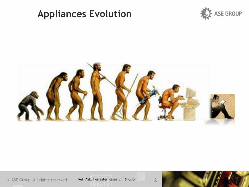
Appliances Evolution
© ASE Group. All rights reserved. 4 Ref: ASE, Forrester Research, 6Fusion
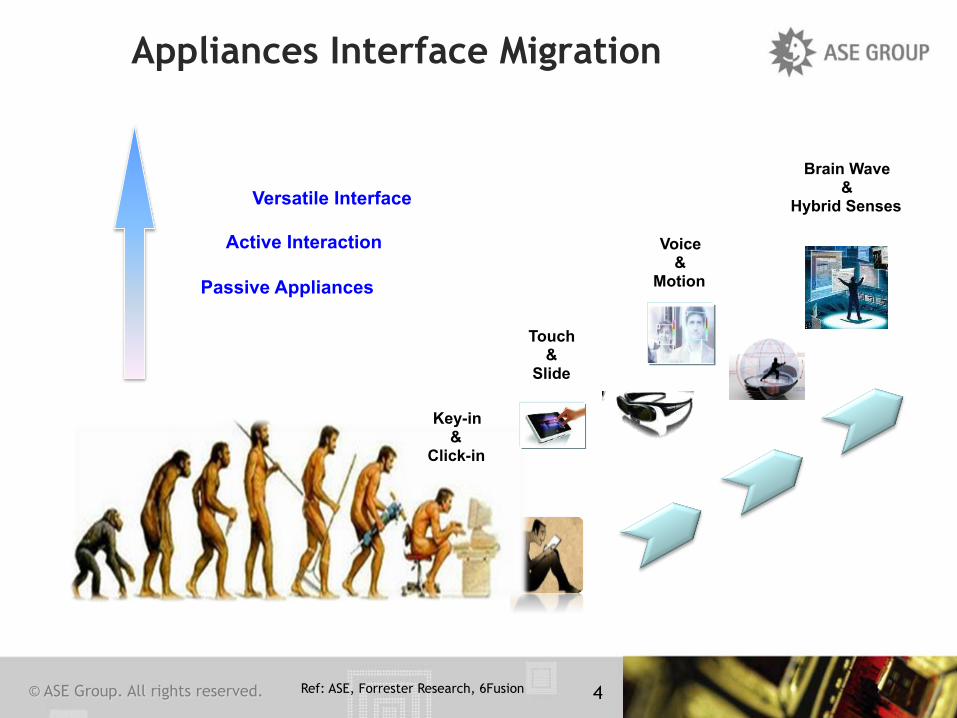
Appliances Interface Migration
Key-in &
Click-in
Touch &
Slide
Voice &
Motion
Brain Wave &
Hybrid Senses Versatile Interface Active Interaction Passive Appliances

© ASE Group. All rights reserved. 5 5
Enriching Life Connection
Data Rate Exabyte / Month
12
6
2011 2012 2013 2014 2015 2016
0.6 1.3
2.4
4.2
6.9
10.8
x17
4C à nC
Robot Personal / Industrial
Real-‐5me Wearable Hybrid Sensing
Intelligent Auto Net
Cogni5ve Communica5on
Smart Grid
Sensor Net
Cloud to Home Network
Cloud to BSN
Cloud for BtB
Handhelds to Cloud
£ Personal à Cloud à Symbiotic Computing & Communications
IoP
IoT
© ASE Group. All rights reserved.
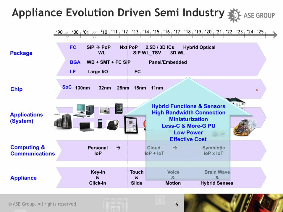
Appliance Evolution Driven Semi Industry
‘90 ‘10 ‘11 ‘12 ’13 ’14 ’15 ’16 ’17 ’18 ’19 ‘00 ‘01 ’20 ’21 ’22 ’23 ’24 ’25
Appliance Key-in
& Click-in
Touch &
Slide
Voice &
Motion
Brain Wave &
Hybrid Senses
Personal à Cloud à Symbiotic IoP IoP + IoT IoP x IoT
Computing & Communications
Applications (System)
Chip
Package
130nm 32nm 28nm 15nm 11nm 7nm
FC SiP à PoP Nxt PoP 2.5D / 3D ICs Hybrid Optical WL SiP WL_TSV 3D WL
BGA WB + SMT + FC SiP Panel/Embedded
LF Large I/O FC
Hybrid Functions & Sensors High Bandwidth Connection
Miniaturization Less-C & More-G PU
Low Power Effective Cost
SoC
6

© ASE Group. All rights reserved. 7
IC Packages Industry-wide Paradigm Shift
LF
BGA
FC & WLP
1984 2013 2001
WB
1995
G1
G2
G3A
High
G3B
Bumping: Leaded Solder → Lead-free Solder → Copper Pillar TSV Tip
G4
• 2.5D & 3D ICs (Bi-model) • Proximity • MEMS SiP++
SiP Stacked Die
PoP Wireless SiP
Embedded SiP
Performance Complexity
SiP+
(Heterogeneous Integration)
• Optical Interconnect (Inter-chip)
• SiP++
• 2.5D & 3D ICs (Uni-model) • MEMS SiP+
2015 2017 2020
• Cu-to-Cu • Micro-solders
MEMS SiP
Cost Driven
Performance Driven
• 2.5D & 3D ICs (Tri-model)
• Optical Interconnect (On-chip)
© ASE Group. All rights reserved. 8
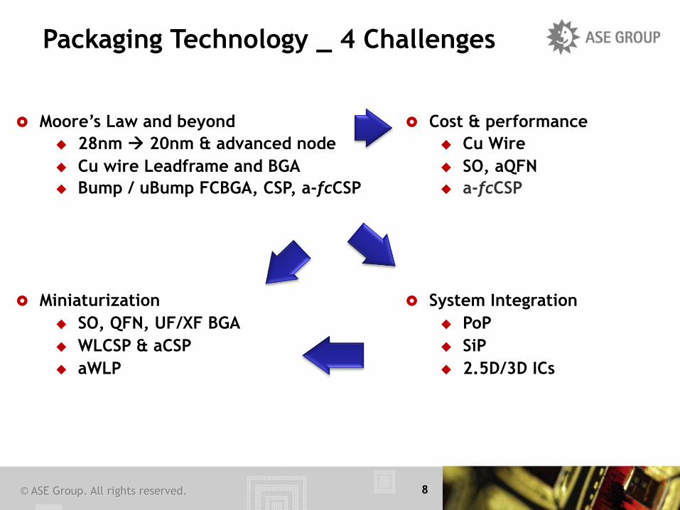
Packaging Technology _ 4 Challenges
£ Moore’s Law and beyond u 28nm à 20nm & advanced node u Cu wire Leadframe and BGA u Bump / uBump FCBGA, CSP, a-fcCSP
£ Miniaturization u SO, QFN, UF/XF BGA u WLCSP & aCSP u aWLP
£ Cost & performance u Cu Wire u SO, aQFN u a-fcCSP
£ System Integration u PoP u SiP u 2.5D/3D ICs
© ASE Group. All rights reserved. 9
2001 130nm
2003 90nm
2005 65nm
2007 45nm
2009 32nm
2011 22nm
2013 15nm
2015 11nm
2017 7nm
2020 à
Transistor (FEOL)
Interconnect (BEOL)
3D Gate Structure
Package Interconnect
Research & Development Multi-layer Transistor
6”/8” à 12” à 18” Wafer Size
Multi-gate structure
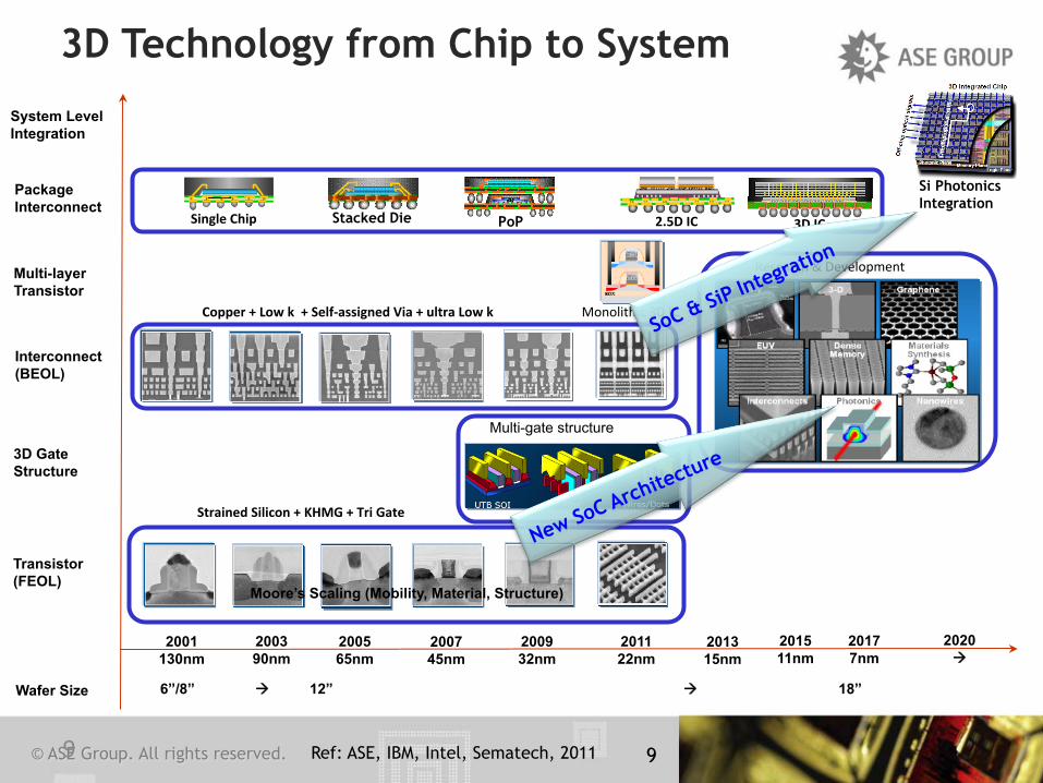
3D Technology from Chip to System
Si Photonics Integration
Monolithic 3D IC
System Level Integration
3D IC 2.5D IC Stacked Die PoP Single Chip
Ref: ASE, IBM, Intel, Sematech, 2011
Moore’s Scaling (Mobility, Material, Structure)
Strained Silicon + KHMG + Tri Gate
Copper + Low k + Self-‐assigned Via + ultra Low k
9

© ASE Group. All rights reserved.
2D & 3D Packaging Technology
1995
SOP QFP
Laminate Substrate in BGAs
Stacked Die FC+WB
QFN Side-by-side WB Chips
3D IC
Leadframe
2000 2014
Side-by-side Flip Chips
Build-up Substrate in FCBGAs
FC + WB
2.5D IC
2D
3D
Chip Pkg
PoP
10
© ASE Group. All rights reserved.
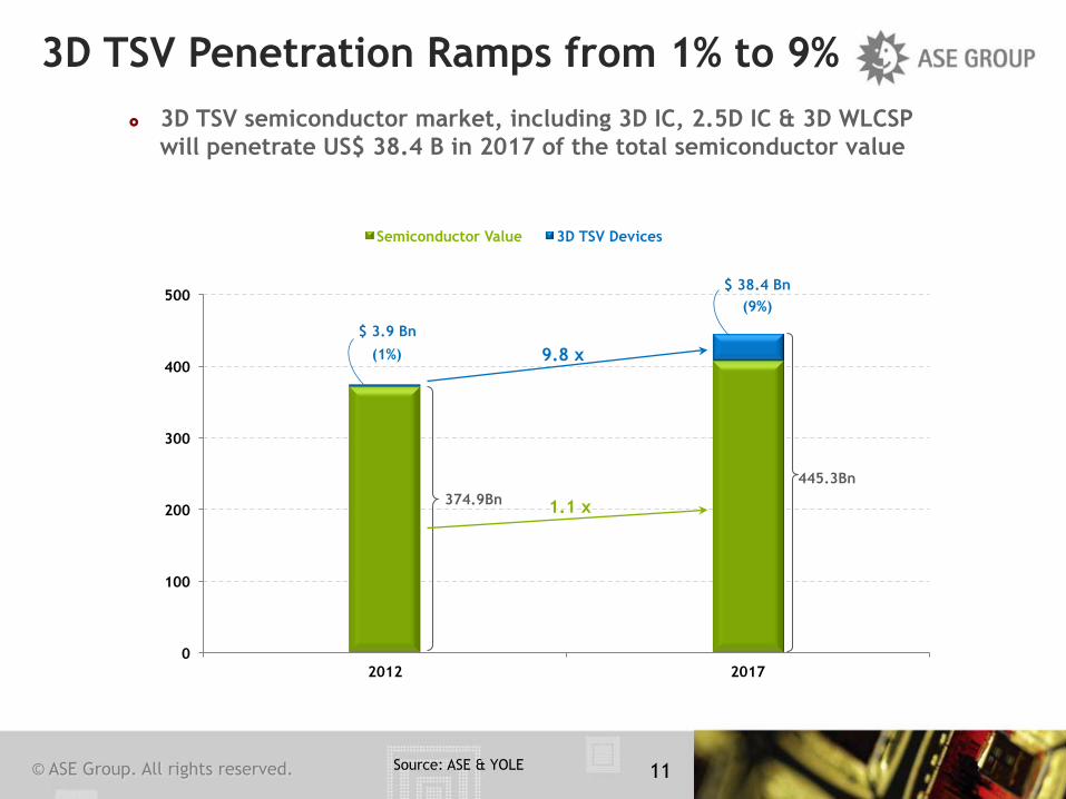
$ 3.9 Bn
$ 38.4 Bn
0
100
200
300
400
500
2012 2017
Semiconductor Value 3D TSV Devices
445.3Bn
(1%)
(9%)
374.9Bn
11
3D TSV Penetration Ramps from 1% to 9% £ 3D TSV semiconductor market, including 3D IC, 2.5D IC & 3D WLCSP
will penetrate US$ 38.4 B in 2017 of the total semiconductor value
Source: ASE & YOLE
1.1 x
9.8 x
© ASE Group. All rights reserved.
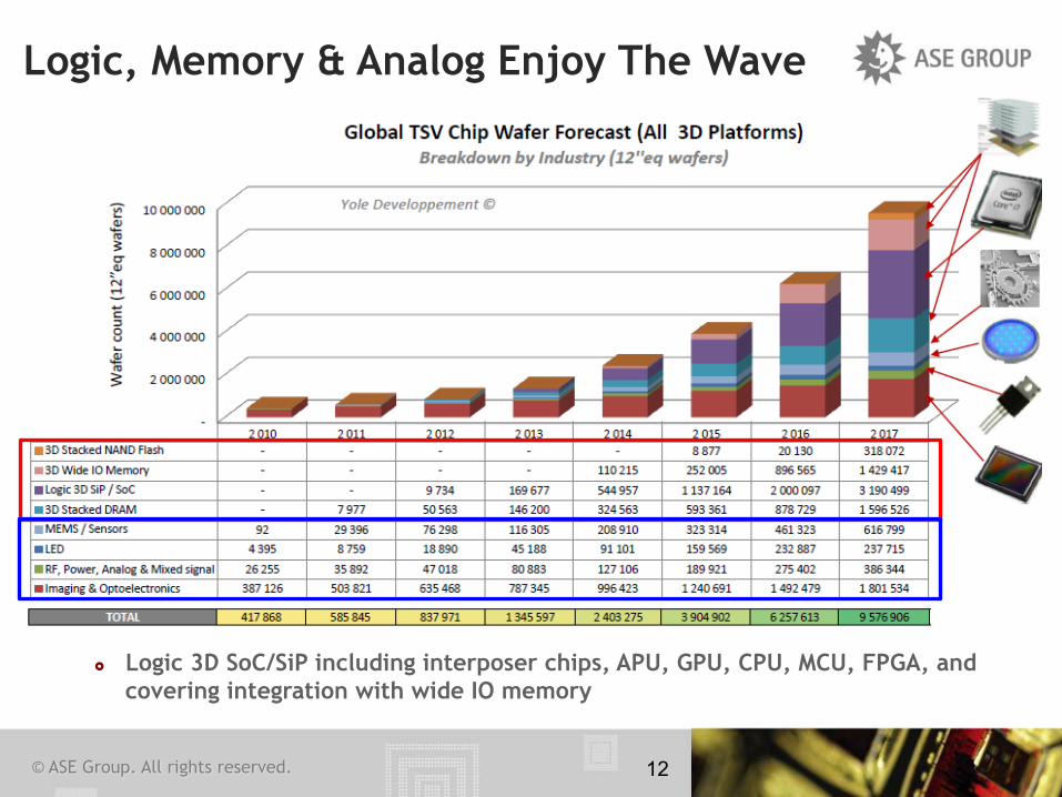
Logic, Memory & Analog Enjoy The Wave
12
£ Logic 3D SoC/SiP including interposer chips, APU, GPU, CPU, MCU, FPGA, and covering integration with wide IO memory

© ASE Group. All rights reserved. 13
2.5D & 3D ICs Enabled “More Than Moore” for IC Developers
2.5D IC
3D IC
System SoC Integration
Stacked SoC Integration

© ASE Group. All rights reserved. 14
Product Type Criteria 200 mm Wafer Readiness 300 mm Wafer Readiness
Y2009 Y2013 Y2009 Y2013
Wafer Thinning / Grinding 50 µm
Via Last
Via Etching 20 ~ 50 µm, AR 10
Via Isolation 20 ~ 50 µm, AR 10
Via Seedlayer 20 ~ 50 µm, AR 10
Via First
Via Etching 5 ~ 10 µm, AR 10
Via Isolation 5 ~ 10 µm, AR 10 Via Seedlayer 5 ~ 10 µm, AR 10
Thin Wafer Handling 50 µm With Carrier With Carrier
Via Surface Finish No Cu Dishing
Re-distribution (Double Sides) -
Micro-bumping 30 µm Pitch
TSV Wafer Probing & Testing 30 µm Pitch 45 um Now 45 um Now
Wafer Singulation -
D2W/W2W Bonding Solder / Micro Bump
Assembly -
Final Test -
Ready for Mass Production Ready for Qualification No Solution Yet
Ready for Prototyping
Source: 2009 Data from ASE’s Dr. Ho Ming Tong in SEMICON Taiwan
Industry 2.5D / 3D ICs Readiness
© ASE Group. All rights reserved.
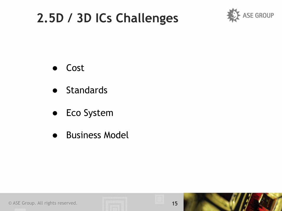
2.5D / 3D ICs Challenges
15
l Cost
l Standards
l Eco System
l Business Model
© ASE Group. All rights reserved.
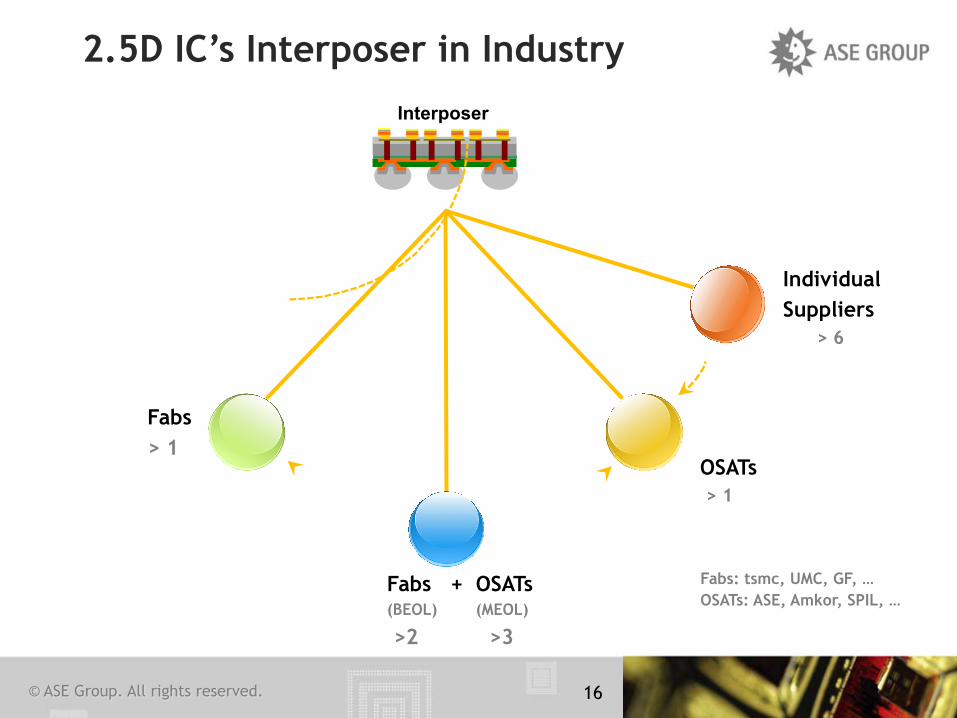
2.5D IC’s Interposer in Industry
Fabs: tsmc, UMC, GF, … OSATs: ASE, Amkor, SPIL, …
Interposer
Individual Suppliers > 6
Fabs > 1
OSATs > 1
Fabs + OSATs (BEOL) (MEOL)
>2 >3
16
© ASE Group. All rights reserved. 17
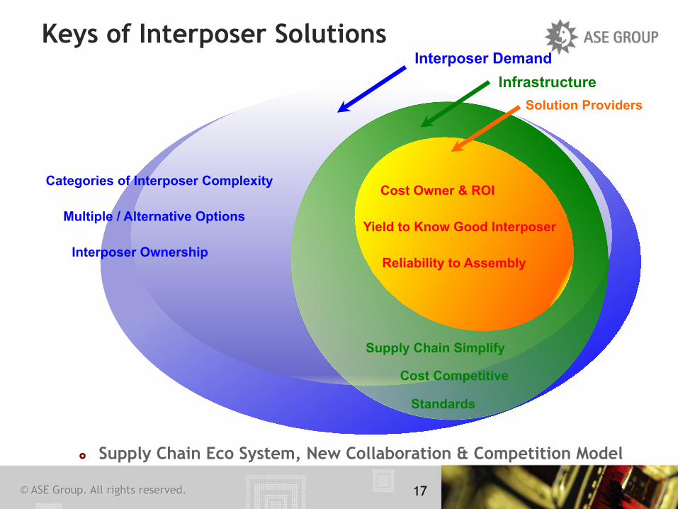
Keys of Interposer Solutions
Multiple / Alternative Options
Interposer Ownership
Categories of Interposer Complexity
Supply Chain Simplify
Cost Competitive
Standards
Infrastructure Interposer Demand
Yield to Know Good Interposer
Reliability to Assembly
Cost Owner & ROI
Solution Providers
£ Supply Chain Eco System, New Collaboration & Competition Model
© ASE Group. All rights reserved. ASE Confidential / Security-C
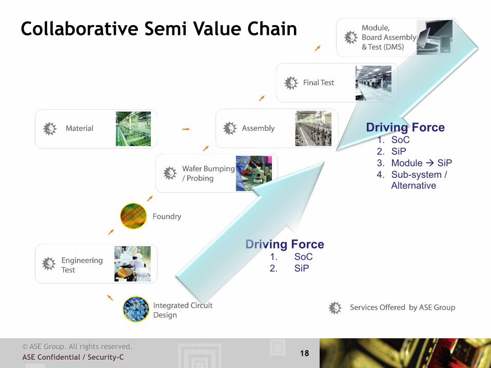
Collaborative Semi Value Chain
Driving Force 1. SoC 2. SiP
Driving Force 1. SoC 2. SiP 3. Module à SiP 4. Sub-system /
Alternative
18

Thank You
Copyright © 2013 by Advanced Semiconductor Engineering, Inc.
All rights reserved.
Other company, product, or service names may be trademarks or service marks of others.
The materials in this presentation may not be reproduced, in whole or in part, in any manner or in any form or otherwise without the written permission of Advanced Semiconductor
Engineering, Inc.
www.aseglobal.com
19