all-optical and logic gate based on 2-d photonic crystal
TRANSCRIPT

International Journal of Communication Systems and Network Technologies
Vol.3, No.2, 2014
DOI-10.18486/ijcsnt.2014.3.2.02 77
ISSN-2053-6283
All-Optical AND Logic Gate Based On 2-D Photonic Crystal
Kajal Bhadel
Dept. of Electronics & Comm. Engineering
Govt. Engineering College Ajmer, Rajasthan.
e-mail: [email protected]
Rekha Mehra
Dept. of Electronics & Comm. Engineering
Govt.Engineering College Ajmer, Rajasthan.
_________________________________________________________________________________________
Abstract — In this paper, All-optical AND logic gate with square cavity in 2-D (two dimensions) photonic crystal
have been proposed. The square cavity is created by removing rods of dielectric GaAs from a rectangular lattice in
air substrate. Photonic crystal (PC) has periodic dielectric structure that has an important characteristic of PC known
as photonic band gap (PBG). The property of PBG is that, wavelength within the band gap cannot propagate through
the crystal. In this research work, this property is used to design an All-optical AND logic gate. The band diagram
gives a good forbidden band gap in the normalized frequency range of 0.554859 ≤ (1/λ) ≤0.811549 for Transverse
Electric (TE) modes. Therefore, band gap width is 0.25669 and normalized central frequency of band gap is
0.6451.The AND optical logic gate is of very small size 13µm×8µm and the operation of this logic gate is verified at
third optical window i. e. 1550 nm, which is the most widely used window in present optical communication system.
Keywords — Photonic Crystal (PC), plane wave expansion (PWE) method, Square cavity, photonic band gap
(PBG), Finite Difference Time Domain (FDTD).
I. Introduction
All-optical logic devices are an indispensable part of
modern integrated optical circuits. There are two ways to
construct optical logic gates: the first one is based on
nonlinear optical effects in Semiconductor optical amplifier
(SOA) [1-10] or periodically poled lithium noibate (PPLN)
waveguide [11-13]. This type of optical logic devices are
based on mature techniques of optical computing but it
requires large space, power consumption and is not feasible
for micro or nano integration. The second one is based on
the use of Photonic crystals. Today photonic Crystal (PCs)
[14] based technology attracts the scientist and researchers
for the realization of optical devices for next generation of
Photonic Integrated Circuits (PICs) [15-17] which can be
implemented in micrometer size instead of centimeter and
millimeter size. Photonic Crystal also used for intelligence
and communication network such as power generation
system: Low-Temperature Thermo photovoltaic, Tunable IR
Camouflage system, High-Power Photonic crystal laser for
Power Beaming.
Photonic Crystals are periodic structures made up of natural
dielectric or artificial materials in which the dielectric
constant changes in one [18-21], two [22-27] or three
dimensions[28-32] to affect the propagation of
electromagnetic waves inside the structures . Because of this
periodicity, PCs exhibit some unique optical properties such
as Photonic band gap (PBG) [33-35] i.e. a frequency
window, similar to the electronic band gap in
semiconductor. Photonic Band Gap (PBG) has been
calculated by plane wave expansion (PWE) method [36]. By
removing rods, we can create a defect [37-39] in the
structure. In this defected structure the periodicity and
completeness of the band gap is tainted and the light cannot
propagate in the PBG region i.e. there are no modes and no
spontaneous emission in this region. Thus, light (Photons)
can be trapped at the defected region with the frequency
corresponding to the defect frequency inside the band gap.
This peculiar behavior will lead to design and realize many
interesting PC based optical components for optical
networking applications and Photonic Integrated Circuits
(PIC). In this paper, a novel approach for design of All
optical AND logic gate is proposed which is based on
photonic crystal square cavity. The propagation of light in

International Journal of Communication Systems and Network Technologies
Vol.3, No.2, 2014
DOI-10.18486/ijcsnt.2014.3.2.02 78
ISSN-2053-6283
the photonic crystal can be numerically simulated by using
the finite-difference time-domain (FDTD) [40] method. The
FDTD method consists of approximating the space and time
derivatives by finite differences in Maxwell‟s equations [41-
42]. Thus, using FDTD method Maxwell‟s equations can be
solved numerically by time stepping the propagation of the
fields. The time step is determined by the Courant limit
along the X and Z directions are Δx and Δz, respectively
(1)
Where
C = speed of light in vacuum i.e. 3x10⁸ m/s
This method has found widespread use in modeling the
wave-propagation in photonic crystals, as it is very
flexible, based on structure geometries and can handle
large index variations.
The complete paper comprises of five sections, II section
describes the design structure and band diagram, III
section elaborates the principal of operation of the design,
section IV explains the simulation and result part and
finally section V concludes the results obtained.
II. Structure Design and Band Diagram
All-optical AND gate have served as sampling gates in
optical sampling oscilloscopes [43] due to their ultrafast
operation compared to conventional electrical methods.
Some application as address recognition, packet-header
modification and data-integrity verification are performed
using AND logic gate. In this paper the 2-D rectangular
lattice is used for designing the All-optical AND logic
gate. In rectangular lattice, the number of rods in X
direction is 25 and that in Z direction is 15. In photonic
crystals, the lattice constant „a‟ i.e. distance between the
two neighbor rods must be in the range of 100nm−1μm.
In this structure a= 540 nm and two types of rods
coupling rods and scatterer rods are used. The radius of
coupling rods are 0.185a, which is closed to 0.1µm and
radius of scatterer rods are 0.203a, which is closed to 0.11
µm. The refractive index of dielectric rods are 3.40 with
permittivity εr =11.56. These rods are surrounded by air
(refractive index=1). Thus, there is high index contrast
ratio between rods and air.
To analyze the behavior of the wave, dispersion diagram
i.e. known as band diagram is studied to have the idea of
band gap. Dispersion diagram, using the plane wave
expansion method (PWE) as shown in figure 1 gives the
propagation modes of the 13µm×8µm photonic crystal
lattice. Photonic crystal structure has a Photonic Band
Gap in the structure without creating defect for
Transverse Electric (TE) modes whose electric field is
parallel to the rod axis. Defect is created for the proposed
design of AND gate. The band diagram gives a good
forbidden band gap in the normalized frequency range of
0.554859 ≤ (1/λ) ≤0.811549 for Transverse Electric (TE)
modes. Band gap width is 0.25669 and normalized central
frequency of band gap is 0.6451.
Figure 1: Band gap for AND logic gate without defect for TE
mode.
Figure 2 shows the proposed structure of All-optical
AND logic gate based on two dimensional photonic
crystal square cavity. This device is designed using
optiFDTD tool of Optiwave software.
Scatterer rods at all the four corners of square cavity are
highlighted using circle. Both point and line defects are
utilized to design All-optical AND logic gate. As
observed from Figure 2 that there are three in-lines quasi
waveguides and a resonant square cavity placed between
them consisting of two rings. This resonant square cavity
possesses dielectric scatterer rods at all the four corners
that provide high spectral selectivity. The coupling rods
are positioned between the in-line quasi waveguide and
resonant square cavity. A Gaussian modulated continuous
wave signal is injected by vertical input plane at the two

International Journal of Communication Systems and Network Technologies
Vol.3, No.2, 2014
DOI-10.18486/ijcsnt.2014.3.2.02 79
ISSN-2053-6283
input ports A and B with the wavelength of 1.55 µm and
the output is observed by placing the observation vertical
line at the output port. The analysis of this All-optical
AND logic gate based on 2-D photonic crystal is done by
varying the radius of scatterer rods and optimizing the
extinction ratio. In addition, power at output port is
optimized with respect to wavelength of operation.
Figure 2: Design of two dimension photonic crystal based All-optical AND logic gate in X-Z plane using optiFDTD.
III. Operation Principle
Figure 3 shows the basic symbol of AND gate. Basic
operation of the AND gate is ,output “ON”(1), when both
inputs are “ON”(1) and output “OFF”(0) ,When any one
input is "OFF” (0). This operation is implemented in All-
optical AND logic gate based on the 2-D photonic crystal. In
All-optical AND logic gate, inputs are applied through
vertical input plane and output is observed by placing the
observation vertical line at the output port. Table 1: shows
truth table of All-optical AND logic gate with the output.
Figure 3: Basic symbol of AND gate
Table 1: Truth table of All-optical AND logic gate
Input
A
Input B Output=A.B Output
power
level
mW/mm
0 0 0 0
0 1 0 1.087
1 0 0 3.903
1 1 1 9.206
IV. Simulation and Results
The computational simulation is carried out by using finite-
difference time-domain (FDTD) method with TE
polarization for the different combinations of the inputs. For
the condition that the input port A is “OFF”, B is “ON” and
vice versa, the output is “OFF”. On the other hand, when the
input port A and B both are “ON” the output is “ON” and
light coming from these input ports, will be coupled in the
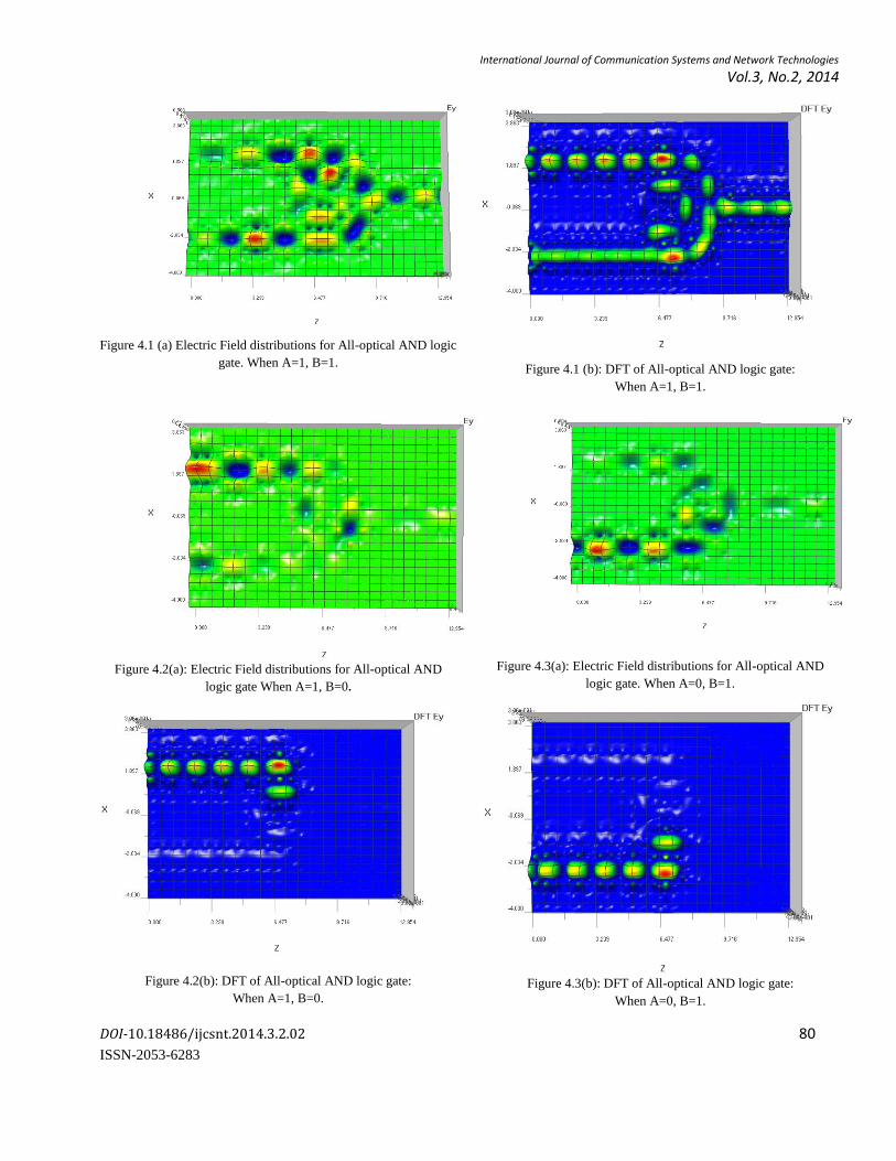
resonant square cavity. Figure 4.1(a & b) shows the
distribution of electrical field and Discrete Fourier Transform
(DFT) when both inputs A and B are "ON". In this case, the
output power level is 9.206 mW/mm. Figure 4.2 (a & b)
shows the distribution of electrical field and Discrete Fourier
Transform (DFT) when the input A is “ON” and B is “OFF”.
In this case, the output power level is 3.903 mW/mm. Figure
4.3 (a & b) shows the distribution of electrical field and
Discrete Fourier Transform (DFT) when the input A is
“OFF” and B is “ON”. In this case, the output power level is
1.087 mW/mm Thus the proposed design has the
characteristics of All-optical AND logic gate which is
verified not only by measurement of power at the output but
also predicted by the Electric field distribution and Discrete
Fourier Transform (DFT) shown in Figure 4.1,4.2 and 4.3.
International Journal of Communication Systems and Network Technologies
Vol.3, No.2, 2014
DOI-10.18486/ijcsnt.2014.3.2.02 80
ISSN-2053-6283
Figure 4.1 (a) Electric Field distributions for All-optical AND logic
gate. When A=1, B=1.
Figure 4.1 (b): DFT of All-optical AND logic gate:
When A=1, B=1.
Figure 4.2(a): Electric Field distributions for All-optical AND
logic gate When A=1, B=0.
Figure 4.2(b): DFT of All-optical AND logic gate:
When A=1, B=0.
Figure 4.3(a): Electric Field distributions for All-optical AND
logic gate. When A=0, B=1.
Figure 4.3(b): DFT of All-optical AND logic gate:
When A=0, B=1.

International Journal of Communication Systems and Network Technologies
Vol.3, No.2, 2014
DOI-10.18486/ijcsnt.2014.3.2.02 81
ISSN-2053-6283
For the proposed design structure, extinction ratio is
measured. Extinction ratio [44] is used to describe the
optimal biasing conditions and how efficiently logic device
works in communication system. Digital optical
communication system, binary data transmit using two
levels of optical power, where the higher power level P1
represents a binary 1 that indicate the light source “ON”
and the lower power level P0 represents a binary 0 that
shows the light source “OFF”. Extinction ratio (re) may be
given by the minimum power of P1 to maximum power of
P0.
(2)
Table 2 and 3 describe the variation of extinction ratio with
radius of scatterer rods and wavelength of input signal
respectively for All-optical AND logic gate.
Table 2: Variation of Extinction ratio with scatterer rod radius for
All-optical AND logic gate.
Scatterer rods radius in
μm
Extinction ratio
re re(dB)
0.08 2.0736 3.1672
0.09 4.0878 6.1148
0.10 3.8508 5.8555
0.11 8.4691 9.2783
0.12 3.8025 5.8006
0.13 2.8664 4.5733
0.14 0.9221 -0.3522
Table 3: Variation of Extinction ratio with input wavelength for
All-optical AND logic gate.
Wavelength of vertical
input in µm
Extinction ratio
re re(dB)
1.40 4.1739 6.2054
1.45 1.5733 1.9681
1.50 2.5521 4.0689
1.55 8.4654 9.2764
1.60 0.5631 -2.4941
1.65 1.5125 1.7969
1.70 0.5090 -2.9328
Figure 5(a) shows the extinction ratio for different scatterer
rod radius. Using this we observed that the maximum
Extinction ratios obtained for scatterer rod radius 0.11µm.
Figure 5(b) shows the extinction ratio for different
wavelength. Using this figure we observed that optimum
performance of All-optical AND logic gate is obtained at
1.55µm wavelength.
Figure 5 (a): Extinction ratio for different scatterer rods radius.
Figure 5(b): Extinction ratio for different wavelength.
International Journal of Communication Systems and Network Technologies
Vol.3, No.2, 2014
DOI-10.18486/ijcsnt.2014.3.2.02 82
ISSN-2053-6283
V. Conclusion
In this paper, we have proposed a design structure of All-
optical AND logic gate based on 2-D photonic crystal
square cavity. Inputs are applied with a vertical input plane
at a line defect of the PCs that are partially transmitted and
reflected by square cavity. This square cavity consists of
four scatterer rods at the corner. The analysis is done by
varying the output power with respect to the radius of
scatterer rods and wavelength of input signal. Using figure
5(a) and 5(b) we analyze that maximum extinction ratio
obtained is at 1.55µm wavelength with 0.11 scatterer rod
radius. While comparing the result of proposed All-optical
AND logic gate with the previous work [45], the result
quoted is that the size of the square lattice is about
15µm*15µm and the power reaches to about 90% of the
input, where as in the proposed design which has small size
of about 13µm*8µm, the power reaches to about 92% of the
input power .Similarly in ref [46], two extra control
waveguides are used and an input signal of 60 W/m is given
but in the proposed design there is no need of extra control
waveguide and the value of input signal applied is also small
i.e. 5.1432mW/mm. The proposed device has a simple and
small structure with clear operating principle which shows
that it is very useful in the ultrafast optical logic operation of
optical digital integrated circuit for future optical network.
REFERENCES
[1] P. Singh, H. K. Dixit, D. K. Tripathi, and R. Mehra, “Design and analysis of all optical inverter using SOA-based Mach-Zehnder interferometer,” Optik, vol. 124, pp. 1926–1929, 2013
[2] P. Singh, D. K. Tripathi, S. Jaiswal, and H. K. Dixit, “Design of all-optical buffer and OR gate using SOA-MZI,” Optical and Quantum Electronics, 2013
[3] Dimitriadou, E. and K. E. Zoiros, "On the feasibility of 320 Gb/s all-optical and gate using quantum-dot semiconductor optical amplifier-based Mach-Zehnder interferometer," Progress In Electromagnetics Research B, Vol. 50, 113-140, 2013.
[4] Dimitriadou, E. and K. E. Zoiros, "Proposal for all-optical NOR gate using single quantum-dot semiconductor optical amplifier-based Mach-Zehnder interferometer," Optics Communications , Vol. 285, No. 7, 1710-1716, 2012.
[5] D. Kong, Y. Li, H. Wang et al., “All-optical XOR gates for QPSK signals based on four-wave mixing in a semiconductor optical amplifier,” Photonics Technology Letters, vol. 24, pp. 988–990, 2012.
[6] L. Lei, J. Dong, Y. Yu, S. Tan, and X. Zhang, “All-optical canonical logic units-based programmable logic array (CLUs-PLA) using semiconductor optical amplifiers,” Journal of Light wave Technology, vol. 30, pp. 3532–3539, 2012.
[7] Y. Aikawa, S. Shimizu, and H. Uenohara, “Demonstration of all-optical divider circuit using
SOA-MZI-type XOR gate and feedback loop for forward error detection,” Journal of Lightwave Technology, vol. 29, pp. 2259–2266, 2011
[8] [K. E. Zoiros and T. Siarkos, “Design rules for full pattern-operated all-optical XOR gate with single semiconductor optical amplifier-based ultrafast nonlinear interferometer,” in Proceedings of the 7th International Symposium on Communication Systems Networks and Digital Signal Processing (CSNDSP '10), pp. 631–635, Newcastle upon Tyne, UK, 2010.
[9] Andalib, P. and Granpayeh, N. All-optical ultracompact photonic crystal AND gate based on nonlinear ring resonators. J. Opt. Soc. Am. B 26(1), 10–16 (2009).
[10] Fujisawa, T. and Koshiba, M. All-optical logic gates based on nonlinear slot-waveguide couplers. J. Opt. Soc. Am. B 23(4), 684–691 (2006).
[11] P. Sahu. All-optical switch using optically controlled two mode interference coupler. Appl. Opt. 51, 2601-2605 (2012)
[12] Zaghloul,Y. A. and Zaghloul. A. R. M. Complete all-optical processingpolarization-based binary logic gates and optical processors. Opt. Express 14(21),9879–9895 (2006).
[13] [Kim, J. Y., Kang, J. M., Kim, T. Y. and Han, S. K. 10 Gbit/s all-optical compositelogic gate with XOR, NOR, OR and NAND functions using SOA-MZI structures.Electron. Lett. 42(5), 303–304 (2006).
[14] C W.Hsu,B. Zhen, S.-L. Chua, S. G. Johnson, J. D. Joannopoulos, and M. Soljačić, “Bloch surface eigenstates within the radiation continuum,” Light: Science & Applications, vol. 2, p. e84, July 2013. Invited paper.
[15] J. C. Hulme, J. K. Doylend, M. J. R. Heck, J. D. Peters, M. L. Davenport, J. T. Bovington, L. A. Coldren, and J. E. Bowers, SPIE Photonics West (invited paper), 8989-6, February 5, (2014)
[16] M. Piels, J. F. Bauters, M. L. Davenport, M.J. R. Heck, J. E. Bowers, Journal of Lightwave Technology, vol. 32, no. 4, pp. 817-823, February 15, (2014)
[17] J. F. Bauters, M. L. Davenport, M. J. R. Heck, J. K. Doylend, A. Chen, A. W. Fang, J. E. Bowers, Optics Express, Vol. 21, Issue 1, January 14, (2013)
[18] Chutinan, and M. Imada, "Trapping and emission of photons by a single defect in a photonic bandgap structure," Nature, Vol. 407, 608-610, 2000
[19] Aghajamali, M. Hayati, C. J. Wu, and M. Barati, “Properties of the defect modes in 1D lossy photonic crystals containing two types of negative-index-materials defects,” Journal of Electromagnetic Waves and Applications, vol. 27, pp. 2317–2329, 2013.
[20] Y. Shen, D. Ye, I. Celanovic, S. G. Johnson, J. D. Joannopoulos, and M. Soljačić, “Optical broadband angular selectivity,”Science, vol. 343, pp. 1499–1501, March 2014.
[21] S. John, “Strong localization of photons in certain disordered dielectric superlattices”, Phys. Rev. Lett., vol. 58, no. 23,pp. 2486-2489, 1987.
[22] J. Riedrich-Möller, L Kipfstuhl, C. Hepp et al.,“One-and two-dimensional photonic crystal microcavities in single crystal diamond,” Nature Nanotechnology, vol. 7, no. 1, pp. 69–74, 2012.

International Journal of Communication Systems and Network Technologies
Vol.3, No.2, 2014
DOI-10.18486/ijcsnt.2014.3.2.02 83
ISSN-2053-6283
[23] M. Kuang, J. Wang, B. Bao et al., “Inkjet printing patterned photonic crystal domes for wide viewing, angle displays by controlling the sliding three phase contact line,” Advanced Optical Materials, vol. 2, no. 1, pp. 34–38, 2014.
[24] S.-L.Chua,L. Lu, J. Bravo-Abad'.J. D. Joannopoulos, and M. Soljačić, “Larger-area single-mode photonic crystal surface-emitting lasers enabled by an accidental dirac point,” OL, vol. 39, pp. 2072–2075, April 2014.
[25] D. Jukić,H. Buljan,D.-H.Lee,J. D.Joannopoulos,and M. Soljačić, “Flat photonic surface bands pinned between Dirac points,”Optics Letters, vol. 37, pp. 5262–5264, December 2012.
[26] J. Lee, B. Zhen, S.-L.Chua, W. Qiu, J. D. Joannopoulos, M. Soljačić, and O. Shapira, “Observation and differentiation of unique high-q optical resonances near zero wave vector in macroscopic photonic crystal slabs,” Physical Review Letters, vol. 109, p. 067401, August 2012.
[27] E. Yablonovitch., “Inhibited spontaneous emission on solid-state physics and electronics”, Phys. Rev. Lett., vol. 58, no. 20,pp. 2059-2062, 1987.
[28] L. Lu, J. D. Joannopoulos, and M. Soljačić,“Waveguiding at the edge of a three-dimensional photonic crystal,” Physical Review Letters, vol. 108, p. 243901, June 2012.
[29] L. Lu, L. L. Cheong, H. I. Smith, S. G. Johnson, J. D. Joannopoulos, and M. Soljačić, “Three-dimensional photonic crystals by large-area membrane stacking,” Optics Letters, vol. 37, pp. 4726–4728, November 2012.
[30] A. Saito et al., J. Nanosci. Nanotechnol., 11, 2785–2792 (2011)
[31] S. Juodkazis et al., Opt. Exp.,19, 7, 5802–5810 (2011).
[32] K.R. Phillips, N. Vogel, I.B. Burgess, C.C. Perry, J. Aizenberg§ , “Directional Wetting in Anisotropic Inverse Opals,” Langmuir, in press (2014).
[33] G. J. Lee, Y.P. Lee, H. Y. Kim, S. Kim and I. Park, “Detailed Treatment of the Nonlinear Optical Properties of Nonlinear Photonic Crystals,” Journal of the Korean Physical Society, Vol. 55, No. 3, 2009, pp. 1237-1242.
[34] Yuan J.H.,Lu Y.Y. 2006 Photonic bandgap calculations with Dirichlet-to-Neumann maps. J. Opt. Soc. Am. 23, 3217–3222.
[35] A. V. Dyogtyev, I. A. Sukhoivanov, and R. M. De La Rue, “Photonic band-gap maps for different two dimensionally periodic photonic crystal structures,” Journal of Applied Physics, vol. 107, no. 1, Article ID 013108, 7 pages, 2010.
[36] K.M. Leung and Y.F. Liu, ”Photon band structures: The plane-wave method,” Phys. Rev. B, vol. 41,pp.10188-10190,1990.
[37] Aghajamali, B.Javanmardi,M. Barati, and C. J. Wu, “Defect modes properties in periodic lossy multilayer containing negative index materials with symmetric and asymmetric geometries structures,”Optik, vol. 125, pp. 839–843, 2014.
[38] Q.Zhu and Y. Zhang,“Defect Modes and Wavelength Tuning of One-Dimensional Photonic Crystal with Lithium Niobate,” Optik, Vol. 120, No. 4, 2009, pp. 195-198.
[39] †Van 't Hoff Laboratory for Physical and Colloid Chemistry, Debye Institute for Nanomaterials Science,
and ‡Biomolecular Imaging, Department of Biology, Utrecht University, Padualaan 8, 3584 CH Utrecht, The Netherlands.Langmuir , 2013, 29 (32), pp 10011–10018.
[40] Allen Taflove. Advances in Computational Electrodynamics, The Finite Difference Time Domain Method. Artech HousePublishers, 1998.
[41] Costabel, M., Dauge, M.: Maxwell and Lam´e eigenvalues on polyhedra. Math. Meth. Appl. Sci. 22,243–258 (1999). DOI 10.1002/(SICI)1099-1476(199902)22:3h243::AID-MMA37i3.3.CO;2-S.
[42] Costabel, M., Dauge, M., Nicaise, S.: Singularities of Maxwell interface problems. M2AN Math. Model. Numer. Anal. 33(3), 627–649 (1999). DOI 10.1051/m2an:1999155.
[43] Andrekson, P. A.; Sunnerud, H.; Hansryd, J. and Li, J. (2005),HighPerformance Optical-Fiber-Nonlinearity-Based Optical Waveform Monitoring,IEEE Journal Lightwave Technology, Vol 23, pp. 2012 – 2022.
[44] NoritsuguYamamoto etal 2005 Jpn.J.Appl.Phys. 44 2575.doi:10.1143/JJAP.44.2575 Received 27 September 2004, accepted for publication 18 November 2004. Published 21 April 2005.
[45] Mortaza Noshad, Amin Abbasi2, Reza Ranjbar,Reza Kheradmand” Novel All-Optical Logic Gates Based on Photonic Crystal Structure” Journal of Physics:ConferenceSeries 350 (2012) 012007 .
[46] Yaw-Dong Wu, Tien-Tsorng Shih, and Mao-Hsiung
Chen. “New all-optical logic gates based on the local
nonlinear Mach-Zehnder interferometer”. Optics
Express, Vol. 16, Issue 1, pp. 248-257 (2008).
[47] Rekha Mehra and Kajal Bhadel. Article: Design and
Simulation of All-Optical OR Logic Gate based on 2-D
Photonic Crystal. International Journal of Computer
Applications 99(6):32-36, August 2014.
[48] Spiros Mikroulis, Hercules Simos, E. Roditi, D.
Syvridis, “Ultrafast all-optical AND logic operation
based on four-wave mixing in a passive InGaAsP-InP
microring resonator”, Ieee Photonics Technology
Letters, Vol. 17 No.9, pp.1878- 1880, 2005.
BIOGRAPHY
Kajal Bhadel is presently working as
assistant professor at Govt. Engineering
College, Ajmer. She has in 6 years of
teaching experience. She has presented
her research work in international
conference with publications in IEEE
(Computational Intelligence and
Communication Networks (CICN), 2014) and International
Journal of Computer Applications (IJCA).
International Journal of Communication Systems and Network Technologies
Vol.3, No.2, 2014
DOI-10.18486/ijcsnt.2014.3.2.02 84
ISSN-2053-6283
Rekha Mehra, presently working
as associate professor and Head
(ECE) at Govt. Engineering
College, Ajmer, is a recipient of
national, state and sponsored
scholarships at school level. She
also received Best Project Award
for project work in BTech
Examination. After completing her
BTech from Allahabad University, she joined as project
engineer (R&D) with Hindustan Cables Ltd., Naini. (Central
Govt. Undertaking) and was later promoted to assistant
manager (R&D). She joined the Govt. Engineering College
as assistant professor (ECE) and was later selected as
associate professor (ECE) in the same institution. She has in
21 years of experience, with 14 years of teaching and seven
years of R&D experience. She is a life member of ISTE,
member of IEEE and fellow of OSI. She was officiating
director at Ajmer Institute of Technology, Ajmer. She has
delivered expert lectures in the field of Optical Fiber
Technology as a resource person in DST workshop
organized by Jai Narayan Vyas University Jodhpur, in
meetings of Ajmer Engineers Institution and in National
conferences. She has presented her research work in
international conferences with publications in refereed
journals. She has reviewed papers of international
conferences with publications in refereed journals and
chaired the technical session in the International and
national conferences