amol ms thesis book - electrical and computer …blj/papers/thesis-ms-gole--terps.pdfabstract title...
TRANSCRIPT
ABSTRACT
Title of Thesis: TERPS: THE EMBEDDED RELIABLE PROCESSING SYSTEM
Amol Vishwas Gole, Master of Science, 2003
Thesis directed by: Professor Bruce L. Jacob
Department of Electrical and Computer Engineering
Electromagnetic Interference (EMI) can have an adverse effect on commercial
electronics. As feature sizes of integrated circuits become smaller, their susceptibility to
EMI increases. In light of this, integrated circuits will face substantial problems in the
future either from electromagnetic disturbances or intentionally generated EMI from a
malicious source.
The Embedded Reliable Processing System (TERPS) is a fault tolerant system
architecture which can significantly reduce the threat of EMI in computer systems. TERPS
employs a checkpoint and rollback recovery mechanism tied with a multi-phase commit
protocol and 3D IC technology. This enables it to recover from substantial EMI without
having to shutdown or reboot. In the face of such EMI, only a loss in performance dictated
by the strength and duration of the interference and the frequency of checkpointing will be
seen.
Various conditions in which chips can fail under the influence of EMI are described.
The checkpoint and rollback recovery mechanism and the resulting TERPS architecture is

stipulated. A thorough evaluation of the design correctness is provided. The technique is
implemented in Verilog HDL using a 16-bit, 5-stage pipelined processor to show proof of
concept. The performance overhead is calculated for different checkpointing intervals and
is shown to be very reasonable (5-6% for checkpointing every 128 CPU cycles).
TERPS: THE EMBEDDED RELIABLE PROCESSING SYSTEM
by
Amol Vishwas Gole
Thesis submitted to the Faculty of the Graduate School of the
University of Maryland, College Park in partial fulfillment
of the requirements for the degree of
Master of Science
2003
Advisory Committee:
Professor Bruce L. Jacob, Chair/Advisor
Professor Virgil D. Gligor
Professor Manoj Franklin

© Copyright by
Amol Vishwas Gole
2003

DEDICATION
To my beloved parents, Lata and Vishwas
and
and all my family and friends
ii

ACKNOWLEDGEMENTS
I am grateful to my advisor, Dr. Bruce Jacob, for his direction and encouragement for
the past two wonderful years here at the University of Maryland. He has not only been a
great academic advisor to me, but has afforded invaluable guidance and insight to life and
its many little quirks. I am sure the knowledge I have gained as being a research assistant
and student under Dr. Jacob’s supervision will help me throughout my professional career.
This work would not have been possible without him. Further, I would like to express my
gratitude towards Dr. Franklin and Dr. Gligor for agreeing to be on my committee.
I would also like to thank Dr. Declaris and Dr. Gansman for their support and the
experience I gained as a teaching assistant under them. I would like to especially thank Dr.
Declaris for always believing in me and his precious guidance. I would also like to thank
the University, the teachers, and the staff for making my Masters Degree a reality.
Working with Cagdas, Sam, and Xia has been a great experience and I would like to
particularly thank them for helping me with this work. I am grateful to Sada and IyerB for
lending their time and ideas when it really counted. I would like to thank my roommates
and friends, Mukul, Spawgi, Anibha, Potti, Chandesaab, Arindam, Hyma, and Priya for all
the support, laughter, dabbas, and putting up with the “Gole Factor” these last few years. I
would like to especially thank Spawgi, Potti, and Priya for being very understanding and
caring during these last few months. I couldn’t have done it without you guys and I hope
our friendship lasts forever.
Finally I am indebted to my beloved parents, Lata and Vishwas, my sister and brother-
in-law, Tina and Vikram, and all my relatives for believing in me and supporting me
throughout especially during the difficult times.
iii
TABLE OF CONTENTS
List of Figures ........................................................................................................... vi
List of Tables .......................................................................................................... viii
Chapter 1 Introduction ....................................................................................... 1
1.1 Effect of EMI on Integrated Circuits..................................................... 1
1.2 TERPS Architecture ...............................................................................4
Chapter 2 Related Work ..................................................................................... 8
Chapter 3 TERPS Architecture ........................................................................ 18
3.1 Checkpointing.......................................................................................18
3.2 Rollback Recovery................................................................................24
Chapter 4 Correctness of Design ...................................................................... 26
4.1 Resuming to a Consistent State ............................................................27
4.1.1 System State and Rollback.......................................................27
4.1.2 Precise Checkpointing..............................................................28
4.1.3 Multi-phase Commit ................................................................29
4.2 Re-execution of instructions .................................................................34
Chapter 5 Implementation ................................................................................ 37
5.1 Basic Processor Architecture................................................................37
5.2 Implementation .....................................................................................39
5.2.1 Logical Verification ..................................................................43
5.3 Safe Storage Implementation ...............................................................46
iv

Chapter 6 Results ..............................................................................................51
6.1 Performance Analysis ...........................................................................51
6.1.1 Performance with the Memory Controller on-chip .................54
Chapter 7 Conclusions and Future Work ......................................................... 56
References ................................................................................................................59
v

LIST OF FIGURES
Figure 1.1: Reduction in feature size over the years ............................................... 3
Figure 1.2: Order of concern for our system-level approach .................................. 5
Figure 3.1: TERPS Architecture .............................................................................19
Figure 3.2: Long latency EMI detection can cause failure of TERPS checkpoint
rollback mechanism ............................................................................ 21
Figure 3.3: Checkpoint rollback mechanism with two safe storage banks .......... 22
Figure 3.4: Checkpointing and rollback recovery using the checkpoint latch,
write buffers and safe storage ............................................................ 23
Figure 3.5: Rollback recovery details .................................................................... 25
Figure 4.1: RF writes do not change permanent state ........................................... 30
Figure 4.2: Store instructions that commit early may change permanent state .....31
Figure 4.3: Multi-phase commit............................................................................. 32
Figure 4.4: Importance of saving store data in the safe storage............................. 33
Figure 5.1: Detailed block diagram of the TERPS Processor Architecture .......... 40
Figure 5.2: Cadence NC Verilog ............................................................................ 43
Figure 5.3: The Design Browser ........................................................................... 44
Figure 5.4: The Waveform view ........................................................................... 45
Figure 5.5: 3 possible SRAM memory cell implementations .............................. 47
Figure 6.1: Performance Overhead due to checkpointing ..................................... 53
vi

Figure 6.2: Performance overhead due to checkpointing with the memory
controller on-chip ............................................................................... 55
Figure 7.1: Photomicrographs of chips fabricated via MOSIS ............................. 57
vii
viii
LIST OF TABLES
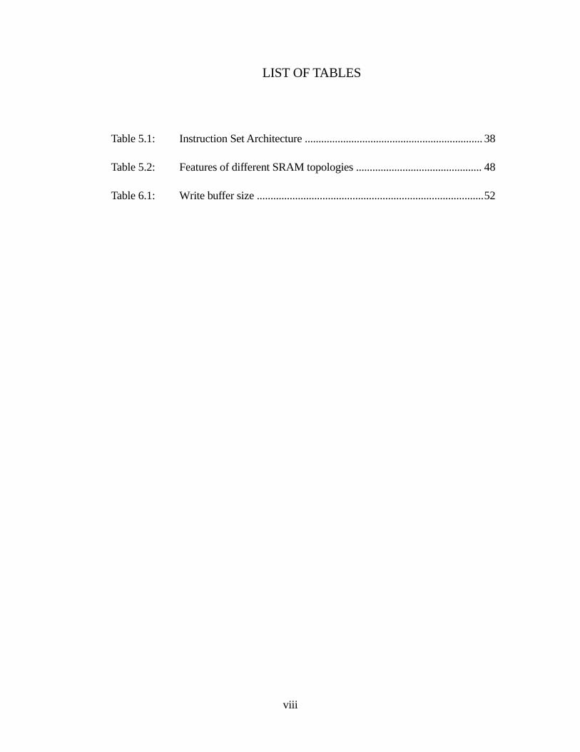
Table 5.1: Instruction Set Architecture ................................................................. 38
Table 5.2: Features of different SRAM topologies .............................................. 48
Table 6.1: Write buffer size ...................................................................................52

Chapter 1
Introduction
Electromagnetic Interference (EMI) broadly refers to any type of interference that can
potentially disrupt, degrade or otherwise interfere with the functioning of electronic
systems. Current high performance ICs like microprocessors are fabricated with very small
feature size, are clocked at frequencies well into the GHz range, and operate at reduced
voltage levels. Though these characteristics have improved the capabilities and
performance of chips, they have increased the susceptibility of high-performance chips to
EMI. Hence, there is a growing concern over the electromagnetic compatibility of ICs in
hostile EMI environments, especially those created by intentionally generated EMI from a
malicious source. The Embedded Reliable Processing System (TERPS) is a system
architecture-based approach which uses a checkpoint rollback recovery protocol to
improve the reliability of microprocessor systems under such extreme operating
conditions.
1.1Effect of EMI on Integrated Circuits
Typical sources of EMI or radio frequency interference (RFI) are overhead high
voltage lines, lightning events, radar devices, powerful radio transmitters, wireless network
devices, and GSM (Global Systems for Mobile communication) bursts. Until recently,
intentionally generated EMI was a lesser concern: In August 1999, the International Union
1

of Radio Science addressed the subject of criminal EMI and EM terrorism which is
defined as “the intentional malicious generation of electromagnetic energy to induce noise
or high-level disturbances into electrical or electronic systems with the intention to disrupt,
confuse, or damage these systems for criminal or terrorist reasons” [1]. In general,
electronic systems are designed more for reduced emissions than for RFI tolerance and
hence they can easily fall prey to intentional EMI. Reports of medical equipment inside
ambulances shutting down at field strengths of 20 V/m due to unintentional interference
are known [1], thus the threat of intentional interference with field strengths of 100 to
200V/m, which can be produced by off-the-shelf equipment from Radio Shack [1], is quite
severe. Moreover, experts claim a suitcase-sized threat is widely available over the internet
[1]. This is introduces serious risks for military equipment, safety-related automotive
systems, and medical equipment because they are greatly reliant on embedded systems,
which are easily susceptible to EMI. As a result, the industry and the research community
are both paying attention to designing systems which not only have low emission
characteristics but also low susceptibility to EMI. Such electromagnetic pollution imposes
new challenges in the design of integrated circuits.
The feature size of ICs has been reducing rapidly over the years (fig. 1.1) in accordance
with Moore’s Law. The electrical charge involved in transistor switching decreases with
the decrease in IC feature size. Correspondingly the energy required to disturb the
switching process reduces, making it easier to disturb the circuit with increasingly lower
EMI signal levels. As the switching speeds of microprocessors increase and supply
voltages scale down resulting in smaller noise margins, the margin of error caused due to
disturbances such as those induced by EMI, drastically reduces putting stress on better
2

signal integrity. Moreover, parasitic effects inside integrated circuits have dramatically
increased making signal integrity a prominent issue [2].
Electronic systems can couple EMI through cables, PCB traces, bonding
interconnects, and even internal metal chip signals like power, ground, and data lines that
behave as receiving antennas [3]. EMI that is coupled by the system can induce currents
(mA) which cause various disturbances. Signal rectification due to interference is caused
by the inherent nonlinear behavior of electronic devices. This is said to be the primary
upset mechanism for integrated circuits under RFI [4]. In addition to signal rectification,
inter-modulation, cross-modulation and other disturbances are immediate effects of
interference [2]. When interpreted as a system signal or superimposed on one, these
disturbances, if powerful enough, can cause malfunctioning or spurious state changes on
logic devices.
Reduction in Feature Size
0.01
0.1
1
10
1970 1975 1980 1985 1990 1995 2000 2005 2010
Year
Lit
hogr
aphy
Figure 1.1: Reduction in feature size over the years. There has been a rapid reduction in IC feature size over the last few decades in accordance with Moore’s Law. As the feature size reduces, the susceptibility of ICs to EMI increases.Source: INTEL and ITRS
(µm
)
3

The power levels and frequency range for which circuits are more susceptible to
intentional EMI have been studied recently. Previous studies observed changes on the I-V
characteristics of diodes, BJTs, and MOSFETs under RFI [5]. Susceptibility levels of a
microcontroller and a DSP chip have been measured for RF interference up to 400 MHz,
and data corruption was observed on the communication path between the microcontroller
and RAM memory [6]. The same study showed that 20dBm RF interference at 350 MHz is
enough to trigger the reset pin of a voltage regulator. Another study investigated the effects
of RF interference on the input ports of a 0.7µm CMOS with frequencies in the 20MHz-
1GHz range with power levels up to 15 dBm [3]. They observed dynamic failures in the
form of variations in input pad propagation delay and static failures when pad output
signals were misinterpreted as they strayed out of the high or low voltage levels. Thus,
even less powerful RFI can cause propagation and crosstalk-induced delays on wires and
can deteriorate signal integrity.
Though electronic equipment can be protected to a certain degree by using shielding,
filters on PCBs, and filtered connectors, an uncompromising necessity to design robust ICs
exists as these measures are often expensive due to post production costs and infeasible for
volume applications [5] as the equipment has to be designed specifically for different
working environments.
1.2TERPS Architecture
This thesis introduces a fault tolerant system architecture, called TERPS, that can
significantly reduce the threat of intentional EMI. In contrast to chip level approaches (e.g.
radiation hardening) or circuit level approaches (e.g. self-checking logic), we investigate a
system-level approach where multi-phase commit protocols are used in conjunction with a
4

safe storage chip, which holds backups of system state and is more EMI resistant than the
CPU and memory controller chips. The resulting system significantly reduces the
susceptibility of its processing components to EMI induced transient faults.
The protection offered to a system’s processing components by the TERPS mechanism
is discussed. Fig. 1.2 outlines the major components of a computer system along with a
safe storage memory, a part of the TERPS mechanism. The CPU is connected directly to
the safe storage via an ECC-protected dedicated bus, which handles the checkpoint
rollback traffic. The memory controller arbitrates the communication between the CPU
and the DRAM system. The CPU, memory controller and safe storage constitute the
Figure 1.2: Order of concern for our system-level approach. The protection scheme we propose in this study will primary cover the processing components of a general computing system. The CPU and memory system are more susceptible to EMI effects as compared to I/O. Therefore our main concern in this study is protecting the processing elements as shown in the figure. Future work will be directed towards I/O transactions.
Memory
Controller
DRAMArrayDRAM
ArrayDRAMArrayD
RA
M
DR
AM
DR
AM
DR
AM
CPUSafe Storage
I/O
Contoller
1st Order EMI effect
2nd Order EMI effect
Current Scope of
immunity offered
by TERPS
5

sphere of protection and, with the DRAMs themselves, represent the area of highest risk
for EMI effects. To increase the reliability of the memory system, the DRAM may be ECC
protected.The processing system is also connected to the I/O system, which represents an
area of slightly reduced risk for EMI effects. A transient fault is more likely to disturb an
in-process computation or memory request than an in-process I/O request because I/O
requests are far less frequent than computations and memory transactions. In addition, the
processor and memory controller operate at much higher speeds and with tighter timing
margins than the I/O system. Hence, we will consider the effects of EMI on processors and
memory systems to be of the first order while those on I/O of the second order. Future
work will be directed towards incorporating the I/O system into the sphere of protection as
well.
Resistance to intentional EMI within TERPS stems from a hardware-based checkpoint
and rollback recovery mechanism that works in conjunction with RF detection methods
[7][8]. This mechanism allows the CPU to rollback to a previously known valid state and
thus protects against a virtually unlimited number of faults anywhere in the area under
consideration. Many embedded systems can tolerate only a limited number of
simultaneous faults and either fail silently or require reboot if more faults occur. This can
have devastating effects if such faults occur during critical conditions, for example if the
guidance system fails while directing a missile or if a pace-maker is affected by a wireless
device. The TERPS architecture allows recovery from such faults without having to reboot
or shutdown and without any human assistance.
To rollback to a safe state, TERPS maintains snapshots, or checkpoints, of the required
system state at predetermined intervals. The processor state is saved into the safe storage
6
memory chip, which is designed to be more resistant to EMI than the CPU and memory
controller by employing circuit, device, and process-level techniques that trade off circuit
performance for noise tolerance. Memory instructions are handled by a series of write
buffers that provide a multi-phase commit protocol to the DRAM system. On EMI
detection, the system is rolled back to a correct state using the safe storage.
As even the minimum required state to rollback is large, it would take many cycles to
do a checkpoint or recovery due to constraints of chip-to-chip bandwidth. To significantly
reduce the impact of checkpointing on performance, high bandwidth solutions like 3D IC
packaging [9], optical interconnect [10], or RAMBUS Yellowstone [11] technologies can
be used. For our physical prototype, we will be implementing 3D IC technology.
Through the application of TERPS, the processing system has improved from one with
many points of failure in the presence of unintentional/intentional EMI to one in which
only the safe storage itself and the CPU-resident control logic that handles the checkpoint
and rollback mechanisms may pose problems.
In this thesis a detailed description of the TERPS mechanism is provided, a proof of its
correctness, implementation considerations are specified, a minimal performance overhead
due to checkpointing is shown, and our physical prototype system, built on 0.5 µm and
0.25 µm processes via MOSIS, is described.
7

Chapter 2
Related Work
Reliability has always been an important component in the design of high performance
processors. A characteristic of a highly reliable system is a low failure rate. A failure
occurs when the behavior of a system deviates from that which is specified for it [12].
Hardware component failures, communication faults, timing problems, human error, etc.
are just a few of the types of faults that occur in systems [12]. Smaller feature sizes,
reduced voltage levels, higher processing speed, and increasingly complex designs have
enhanced the functionality of digital systems but have also made them prone to hardware
related faults during execution. A study by Randell et al. [12] provides an insight to
reliability issues including types of faults, fault tolerance techniques, and examples of fault
tolerant systems. They classify hardware component failures by duration (fault is
permanent or transient), extent (effect is localized or distributed), and value (creates fixed
or varying erroroneous results).
Peercy and Banerjee discuss fault detection in detail [13]. Fault detection requires
redundancy in either space, time, information, or algorithm. Space redundancy is usually
some form of n-modular redundancy (nMR) or complementary logic. As chip area is
expensive, an alternative is time redundancy where the same circuit is used for the same
functionality at two different times. The major drawbacks are that permanent faults cannot
8

be detected and the throughput is lowered. Watchdog timers are also used to guarantee that
a processor is making forward progress. Information redundancy is in the form of
concurrent error detecting codes like parity check codes, Berger code, and M-out-of-N
code. Algorithm-based fault tolerance introduces some information or time redundancy
into an aspect of the function being performed by the VLSI circuitry. Manoj Franklin’s
study [14] investigates ways to implement redundancy techniques for superscalar
processors. Under utilized resources available on the system are used to incorporate
hardware, information, or time redundancy to detect errors in the functional units. REESE
[15], which is a method of soft error detection in microprocessors, detects transient faults
using time redundancy and adds a small number of extra functional units to keep the
execution overhead low. A special form of space and time redundancy is observed in the
DIVA architecture [16][17]. The core processor is appended by a small and simple checker
processor which is functionally the same only less powerful. If any results from the core
processor are incorrect due to a fault of some kind, the checker will be able to detect and
fix the errant result. It then flushes the core processor state and restarts it after the errant
instruction. This is an elegant solution for solving a whole range of faults while also
reducing burden of verification. However, it cannot be applied for EMI induced faults as
these may persist everywhere in the chip i.e. the checker processor, the RF and the clock
network may go bad leaving no valid state to restart from.
In general, a system can be designed to be fault tolerant by some form of redundancy
and error recovery algorithms. Once an error is detected, fault tolerant techniques use some
form of forward or backward error recovery [12]. Forward error recovery is dependant on
9

having identified the fault, or at least all its consequences. Such schemes attempt to make
use of the erroneous system state to make further progress (e.g. Error Correcting Codes).
Backward error recovery techniques require establishing recovery points during which
the state is saved (checkpointing) in a safe location and can be later reinstated (rollback-
recovery). Checkpointing and rollback-recovery has always been a commonly applied
fault tolerance approach in the development of highly reliable processing systems.
Depending on how much time is allowable for recovery procedures and how much loss of
work is acceptable, checkpointing and rollback-recovery is implemented in software or
hardware.
One of the most significant and earliest systems which adopted checkpointing and
rollback recovery were intended for space applications in which a high degree of fault
tolerance was essential. The Jet Propulsion Laboratory Self Testing and Repairing (JPL-
STAR) computer [18] was a general purpose fault tolerant computer developed for a
spacecraft guidance, control and data acquisition system which would be used on long
unmanned space missions. Upon error detection by redundant units, error recovery is
initiated by backward error recovery in software. The programs established recovery
points and decided on the state that needs to checkpointed. File systems, database systems,
and distributed systems also rely on checkpointing and rollback to establish fault tolerance.
Koo and Toueg [19] disclose a distributed algorithm to create consistent checkpoints, as
well as a rollback-recovery algorithm for distributed systems. They identify the “domino
effect” and “livelocks” problems related with checkpoint creation and rollback-recovery in
distributed systems and then show how their algorithm solves these problems by tolerating
failures during their execution and forcing a minimal number of processes to rollback after
10
a failure. Chandy and Ramamoorthy [20] discuss optimum checkpointing strategies in
order to have shorter recovery times but still not affect performance significantly. The
rollback points are tailor-made for a particular program according to their algorithm.
Upadhyaya and Saluja [21] later modified Chandy and Ramamoorthy’s algorithm to insert
rollback points in programs with multiple retries and also added a watchdog processor for
error detection. The watchdog processor is implemented in place of a software error
detection solution to ensure low error latency. K. Shin et al. [22] developed models to
evaluate the behavior of checkpointing of real-time tasks. Using these models they
determined optimal intercheckpoint intervals and an optimal number of checkpoints for a
task by minimizing the mean task completion subject to a specified confidence in
execution results. For their realistic model, which includes imperfect coverages of both the
on-line detection mechanism and the acceceptance test, they observed that if a task
requires a high probability of correct execution results, checkpointing must be done more
frequently towards the end of the task, since the task has to pass all the acceptance tests
near the end of the task.
In this research, we focus on environments where error rates are high and real-time
constraints prohibit significant delays for recovery. These constraints motivated us to use a
hardware-assisted backward error recovery scheme - instruction retry - for TERPS.
Instruction retry is used for rapid recovery from transient faults and is seen in many
systems including the IBM 4341 processor [23], C.fast [24], the IBM ES/9000 Model 900
[25], and in the UCLA Mirror Processor [26]. In single instruction retry, the state of the
processor is checkpointed at each instruction boundary, and upon error detection, the state
is rolled back to the previous instruction state. However this requires immediate error
11

detection. In the IBM 4341 processor [23], an instruction is retried by restoring state
information that is continuously saved and removed by hardware. If the instruction is to be
aborted, the “machine check interrupt process” is provided with a damage report. Tsao et
al. introduce C.fast, a VLSI fault tolerant processor [24] in which shadow registers that
contain state of the previous instruction are attached to every state register on the chip.
When an error is detected during the execution of an instruction, the processor is able to
retry the same instruction immediately.
However, concurrent error detection required for single instruction retry, demands
checkers and isolation circuits in communication paths between different modules of the
system. These systems can incur significant performance penalties due to the delays in
checking. To erase this performance loss, error checking can be done in parallel. The side
effect is that the error signal is delayed and recovery becomes more complicated. Multiple
instruction retry - rolling back multiple instructions - is called for in response to a delayed
error signal. Multiple instruction retry schemes can either employ full checkpointing or
incremental checkpointing [27]. In full checkpointing, which is employed by TERPS,
snapshots of the system state are established at regular or predetermined intervals, and the
system can roll back to this saved state on error detection. In contrast, incremental
checkpointing preserves system state alterations in a sliding window like manner; error
detection initiates recovery by undoing the system state changes one instruction at a time,
back to an instruction previous to the one in which the error occurred. The Model 900 [25]
uses a form of incremental checkpointing by postponing the remapping of physical register
until the error detection latency has been exceeded for the data contained in the physical
register. Checkpoints of the system state are made at variable intervals. Though the
12
processor has an out-of-order model, in-order completion is maintained by storing the
results of instruction that finished out-of-order in temporary registers. If one of the
processors fails due to some fault, its processing state is rolled back to a consistent error
free state by purging the pipeline and temporary registers. Micro rollback is another
interesting incremental checkpointing based multiple instruction retry concept which was
introduced by Tamir et. al. [28][29]. Micro rollback is the process of backing up a system
several cycles in response to a delayed error signal. In micro rollback each module must
save the state required to properly recover. In the UCLA Mirror Processor (MP) [26]
system two mirror processor chips operate in lock-step, comparing external signals and a
signature of internal signals every clock cycle. On error detection, both processors either
recover using micro rollback or, in certain cases, erroneous state is corrected by copying a
value from the fault-free processor to the faulty processor. The MP was designed to
recover from single transient faults (with support for some multiple faults also) which are
detected by having 2 processors, i.e. 2-modular redundancy. The MP works to recover as
soon as an error is detected to prevent the spread of erroneous information throughout the
system, i.e. error confinement. TERPS does a system-level recovery and prevents errors
from spreading throughout the system as the state is never completely committed until it is
safe to do so. Unlike the MP, TERPS does not take checkpoints at every clock cycle and
does not recover to exactly the clock cycle before the error. But TERPS is similar to the
MP in that it also uses write buffers to support the rollback mechanism when encountering
store instructions.
The aforementioned hardware-based instruction retry schemes employ some form of
data redundancy to eliminate rollback data hazards leading to hardware overhead.
13

Compiler-based multiple instruction retry techniques [30] have been developed to reduce
hardware costs by alleviating anti-dependencies by data flow transformations that result
from multiple instruction rollback. However, compiler-assisted instruction retry [27][31],
which utilizes a read buffer to eliminate one kind of rollback data hazard and compiler
techniques to eliminate the remaining hazards, shows better performance as compared to
the compiler-only instruction rollback scheme by exploiting the unique characteristics of
different hazard types.
Instruction retry has the disadvantage that changes have to made in the processor
design. Bowen and Pradhan introduced a scheme that supports checkpointing and rollback
recovery at a higher level; checkpoint and rollback was embedded directly into the
translational lookaside buffer (TLB) [32]. In this scheme, a backup copy of a memory page
is made just before it is modified. This requires large checkpointing intervals to minimize
the overhead due to page manipulations and modification of the TLB. Cache-Aided
Rollback Error Recovery (CARER)[33] is a cache-based checkpointing proposal wherein
the replacement policy of the regular cache is modified such that it prevents the
replacement of dirty data thereby keeping a checkpoint state in memory. When either the
deletion of some of the dirty blocks becomes unavoidable, an external interrupt occurs, or
an I/O instruction is executed, a checkpoint is established by saving the processor state in
internal back up registers and marking all the dirty blocks as unchangeable. When an error
is detected, the processor recovers by restoring its saved state and all cache blocks, while
the unchangeable ones are marked invalid. TERPS also employes a similar approach
where the write buffers act as cache and hold the store instruction data to prevent them
from being committed to memory. However TERPS does not use the modified
14

replacement policy used by CARER to save state as it stores the checkpointed state in an
external safe storage memory. An excellent performance study on cache-based recovery
schemes is presented by Janssens and Fuchs [34]. They stipulate that though the average
overhead of cache-based recovery schemes is quite minimal, the performance is not
predicable as compared to a system without recovery capability due to the lack of control
and variability of the checkpoint frequency of different programs and caches; checkpoint
frequency will vary according to the I/O behavior and program’s interaction with the
memory. TERPS has a constant checkpoint frequency and it is shown that the performance
impact is predicable across different programs. This is crucial for real-time systems where
a predictable recovery behavior would assist a scheduler to schedule programs to meet
their deadlines even in the presence of a fault.
Support for checkpointing and rollback recovery in shared memory multiprocessor
environments have also been proposed [35][36][37]. Wu et al. [35] present a cache-based
checkpointing and recovery algorithm to maintain a consistent checkpoint state. The use of
checkpoint identifiers and recovery stacks along with private caches was shown to reduce
performance degradation due to increased write-backs. In the ReVive scheme [36],
complex checkpoint and rollback functions are performed in software, while hardware
operations are limited to the directory controllers of the machine to reduce costs. During a
global checkpoint, the caches are flushed to memory and a two-phase commit protocol is
performed. Therefore the main memory contains the checkpoint state. Changes to the
checkpoint state in the memory are logged by the home directory controller and are used to
restore the memory state upon error detection. ReVive performs recovery from a wide
range of failures without any hardware modification to the processors or caches. SafetyNet
15

[37] is a fault tolerant solution which maintains multiple, globally consistent checkpoints
of a shared memory multiprocessor and minimizes performance overhead by pipelining
checkpoint validation with subsequent parallel execution. The current uni-processor
TERPS form can be extended to a multi-processor environment utilizing architectures
similar to SafetyNet [37] as it also can sustain long latency error detection mechanisms.
Checkpointing and rollback was proposed by Hwu and Patt for branch mis-prediction
and exception handling in out-of-order processors [38]. They proposed cost-effective
algorithms for performing checkpoint repair which incur very little overhead in time.
Smith and Pleszkun introduced novel structures for implementing precise exceptions in
pipelined processors [39]. When an exception occurs, the process state must be saved such
that it reflects the sequential architectural model. Primarily, the saved state must reflect the
following conditions: (i) All instructions preceding the instruction indicated by the saved
program counter have been executed and have modified the process state. (ii) All
instructions following the instruction indicated by the saved program counter are
unexecuted and have not modified process state. (iii) The saved program counter points to
the interrupted instruction. One can recognize that the concepts of precise exception
handling in pipelined processors can be used to ensure that during checkpointing, a precise
state is saved.
TERPS has been developed borrowing the checkpointing and rollback concepts
applied in the software and hardware of many fault tolerant systems and the conditions for
precise exceptions in pipelined machines for providing a precise rollback state. Fault
tolerant architectures that have been proposed previously have mainly concentrated on
protecting systems from single error transient faults while TERPS has been designed
16

keeping in mind that EMI induced faults may occur everywhere in the system. This
disparity is the main reason behind the differences in contemporary fault tolerant designs
and TERPS.
17

Chapter 3
TERPS Architecture
As stated earlier, there is a growing concern over the electromagnetic compatibility of
ICs in hostile EMI environments, especially those created by intentionally generated EMI
from a malicious source. EMI can couple through various parts of a system and, if
powerful enough, can cause misinterpretation of data, clock edges and even the power and
ground references. This can result in failures in many sections of the chip at the same time.
Related works have aimed at solving single error or a limited number of faults and hence
are not directly applicable as a solution to this problem. TERPS is a system architecture-
based fault tolerance approach that addresses the issues related with EMI induced faults
with little performance overhead. It allows recovery from such faults without having to
reboot or shutdown and without any human or even software assistance. A description of
how the architecture efficiently implements the hardware-based checkpoint rollback
recovery mechanism is provided in detail in this chapter.
3.1Checkpointing
The minimal process state required to return to any point of execution varies from
processor to processor, but in general it comprises of the program counter, the register file,
and a window of memory transactions. For precise checkpointing the saved process state
18

must be consistent with the sequential architectural model. The issues dealt with here are
similar to those by Smith and Pleszkun [39].
First a system overview of the various elements of the TERPS architecture are
highlighted in fig 3.1. In addition to the CPU chip and memory system, a special safe
storage chip is augmented to the basic system architecture. The CPU is connected directly
to the safe storage via a dedicated bus to handle the checkpoint rollback traffic. This bus
may be ECC-protected to protect against single error transient faults. The memory
controller arbitrates the communication between the CPU and the DRAM system. The
CPU, memory controller and safe storage constitute the sphere of protection offered by
TERPS currently and, with the DRAMs themselves, represent the area of highest risk for
EMI effects. To implement the mechanism, the processing system has a checkpoint latch
Figure 3.1: TERPS Architecture.
Processor Core
SS A
SS B
Che
ckpo
int L
atch
Write Buffers
Memory Controller
DRAMArrayDRAM
ArrayDRAMArray
DR
AM
DR
AM
DR
AM
DR
AM
Safe Storage Chip
CPU_CLK
SS_CLK
Buffer
WB0-2
ss_clk
CPU_clk
CPU chip
state latched on CPU side
state latched on SS side
chkpt_rollback bus
19

and a series of write buffers. This processing system is also connected to the I/O system
(fig. 1.2), which as explained earlier represents an area of slightly reduced risk for EMI
effects. Future work will be directed towards incorporating the I/O system into the sphere
of protection as well.
In order for the safe storage to be less susceptible to EMI, it applies circuit, device, and
process-level techniques that trade off circuit performance for noise tolerance and hence
operates at a frequency much lower than the CPU. The safe storage clock (ss_clk) is
stepped down from the CPU clock (CPU_clk) and is given a duty cycle designed to
maximize setup and hold times available to the safe storage. For the purposes of the
discussion let us take the time period of the ss_clk as N times longer than the CPU_clk, i.e.
Tss_clk = N * TCPU_clk. Due to this speed mismatch and differences in process technology,
the process of checkpointing is not a straightforward one. The safe storage must latch a
value from the CPU at a clock speed dictated by its technology’s characteristics, else its
setup and hold times might be violated if, for example, the data is held valid on the bus for
a time equal to the period of CPU_clk and that time is less than the setup and hold times
required by a safe storage. Hence when a precise checkpoint is taken at the CPU side, the
process state is first stored in a checkpoint latch. If no fault is detected, the safe storage will
read the state from the checkpoint latch at every positive edge of the ss_clk. It is important
to note that EMI detection will not be concurrent and will probably take a few CPU clock
cycles. This leads to problems when a fault happens just before the safe storage reads the
state from the checkpoint latch, and the fault is detected only after this action. The saved
state in the safe storage may be polluted and the system would not be able to recover from
that state. This problem is depicted in fig 3.2.
20

Therefore, when recovery is necessary, we have to rollback to an older valid
checkpoint. To satisfy this condition, the safe storage has two banks and will store the
checkpointed state in either safe storage A or safe storage B in an alternate fashion
allowing it to maintain the last two checkpoints. This modified checkpoint rollback
mechanism can be visualized in Fig. 3.3. This design is compatible with an EMI detection
circuit which can report the fault within at most N CPU clock cycles. Hence checkpointing
is done every N CPU cycles.
Store instructions must be prevented from writing their data to permanent storage
before it is known whether the store data is error-free or not. By delaying the stores from
committing, load instructions that are re-executed after a recovery will not read the wrong
data. A multi-phase commit protocol has been employed to delay the store data by
Figure 3.2: Long latency EMI detection can cause failure of TERPS checkpoint rollback mechanism. The TERPS checkpoint rollback recovery mechanism can be explained using the safe storage clock (ss_clk) as a reference. At point R the state is checkpointed at the CPU and written to the safe storage at point Q as shown. Then at point S a new checkpoint is made by the CPU and this state is stored in the safe storage at point T overwriting the last checkpointed state R. If a fault actually occurs just before point T and was detected only afterwards due to the long latency EMI detection, the state saved in the safe storage may be corrupt which is indicated by S*. When the system initiates recovery at point C, it will reinstate the bad state S* into the system and recovery will correspondingly fail. To operate correctly, the system should be able to rollback to state R.
Rollback
ss_clk
R CQ S T
:Fault Detected
xSafe Storage
R S* S*
Fault Actually Occurs
21

directing it through a series of three write buffers and the memory controller before they
are actually written to memory. As we are rolling back to the older checkpoint, we need 3
write buffers to ensure that no write instruction is committed to permanent state until it is
safe to do so. Justification for using three write buffers is provided in the following chapter
where correctness of the design is addressed. The interaction of the checkpoint latch, write
buffers, and safe storage is shown in fig 3.4. During every checkpoint interval on the CPU
side, stores write to the first write buffer, WB0. On average about 30% of all instructions
are memory transactions and about one-third of those are stores [40]. Therefore the size of
the write buffer can be roughly decided by the frequency of checkpointing, e.g. if a
checkpoint is made every 128 CPU cycles, then the write buffer size can be set around 12-
entries. In the worst case, if the write buffer becomes full, the pipeline is stalled until the
next checkpoint. During a checkpoint the contents of WB0, i.e. the store instructions that
were executed in this last checkpoint interval, are written to the checkpoint latch. Also the
Figure 3.3: Checkpoint rollback mechanism with two safe storage banks. At point R the state is checkpointed at the CPU and written to the safe storage A (SS A) at point Q. Then at point S a new checkpoint is made by the CPU and this state is stored in the safe storage B (SS B) at point T. The CPU initiates another checkpoint at point U. Note that since a fault is detected sometime before point C, the checkpoint made at U is not latched in the SS A. At this point the safe storage contains checkpoints made at points R and S in SS A and SS B respectively. As the fault detected before point C may have occurred in the interval Q and T due to delays in the detection circuit, the system recovers to point R and not S.
Rollback
ss_clk
R CQ S T U
:Fault Detected
R
x
R
S
R
S
x
x
SS A
SS B
22
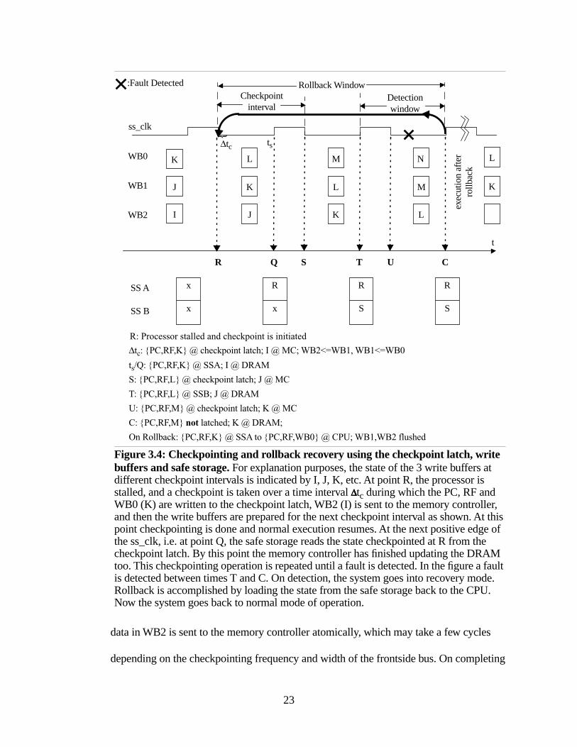
data in WB2 is sent to the memory controller atomically, which may take a few cycles
depending on the checkpointing frequency and width of the frontside bus. On completing
Figure 3.4: Checkpointing and rollback recovery using the checkpoint latch, write buffers and safe storage. For explanation purposes, the state of the 3 write buffers at different checkpoint intervals is indicated by I, J, K, etc. At point R, the processor is stalled, and a checkpoint is taken over a time interval ∆∆∆∆tc during which the PC, RF and WB0 (K) are written to the checkpoint latch, WB2 (I) is sent to the memory controller, and then the write buffers are prepared for the next checkpoint interval as shown. At this point checkpointing is done and normal execution resumes. At the next positive edge of the ss_clk, i.e. at point Q, the safe storage reads the state checkpointed at R from the checkpoint latch. By this point the memory controller has finished updating the DRAM too. This checkpointing operation is repeated until a fault is detected. In the figure a fault is detected between times T and C. On detection, the system goes into recovery mode. Rollback is accomplished by loading the state from the safe storage back to the CPU. Now the system goes back to normal mode of operation.
Rollback Window:Fault Detected
J
KWB0
WB1
WB2
L
K
K
L
M
L
M
I
N
J
ss_clk
t
∆tc ts
{
L
K
exec
utio
n af
ter
rollb
ack
Detection window
R C
Checkpoint interval
Q S T U
∆tc: {PC,RF,K} @ checkpoint latch; I @ MC; WB2<=WB1, WB1<=WB0
ts/Q: {PC,RF,K} @ SSA; I @ DRAM
S: {PC,RF,L} @ checkpoint latch; J @ MC
T: {PC,RF,L} @ SSB; J @ DRAM
U: {PC,RF,M} @ checkpoint latch; K @ MC
C: {PC,RF,M} not latched; K @ DRAM;
On Rollback: {PC,RF,K} @ SSA to {PC,RF,WB0} @ CPU; WB1,WB2 flushed
R: Processor stalled and checkpoint is initiated
R
x
R
S
R
S
x
x
SS A
SS B
23

this transaction, WB2 will be overwritten by WB1 and WB1 by WB0. WB0 is ready for
the store data that will follow. The memory controller begins writing stores to the DRAM
and normal execution resumes.
Note that in the TERPS architecture an instruction is declared committed when its
result is out of the safe storage and hence into permanent state. An instruction, whose
results are reflected in the older checkpoint saved, is ready for committal only after it is
sure that the newer checkpoint that was saved is ensured to be valid and the system will be
able to rollback to it in case of a fault. This defines a rollback window, which is the
minimum lifetime of an instruction, i.e. any instruction checkpointed at a given rollback
point can not be committed before it is out of the rollback window. For example, in fig.3.4,
instructions checkpointed at rollback point R can be committed to permanent state only
after commit point C if there is no fault detected.
3.2Rollback Recovery
When the EMI detection circuit indicates a fault, the pipeline is stalled until the rising
edge of safe storage clock to prevent the system from executing instructions that may be
faulty. At this point the system goes into recovery mode and the pipeline is immediately
flushed to remove the corrupted state. The safe storage is prevented from reading the
checkpoint latch, as it would during normal operation, so it does not save the state that
could have been polluted. Instead, after sufficient bus turn-around-time, the safe storage
output buffers are enabled to provide the valid state to the CPU. As the safe storage is
running at a much slower clock, the CPU will wait until the safe storage is able to drive its
output buffers. Once ready, the CPU latches the data from the safe storage and normal
operation is resumed. A detailed timing diagram of the rollback recovery procedure is
24

shown in fig. 3.5. It can be seen that the rollback penalty is four checkpoint intervals. Note
that no matter where within a certain detection window a fault is detected, the system will
always recover to the same rollback point corresponding to that detection window.
Figure 3.5: Rollback recovery details. A timing diagram of the recovery procedure is highlighted with the aid of the Recovery mode signal, safe storage select signal, and checkpoint rollback bus. When a fault is detected, the system goes into Recovery mode at the next rising edge of the ss_clk. After bus turn around time, the safe storage puts the rollback state onto the checkpoint bus and it is read by the checkpoint latch. Again the bus is turned around and normal operation is resumed utilizing the saved state. At the beginning of every checkpoint interval the safe storage select (ss_sel) line, which selects which bank of the safe storage to write/read from is toggled. But when the system is in Recovery mode, it is not toggled as it is already pointing to the bank with the older state from which the processor will read instead of write during recovery. After recovery, ss_sel is toggled as usual hence causing the system to overwrite the newer saved state (S). This is convenient as newer state (S) may be corrupted due to he issues discussed previously with regard to delay in detection.
R CS U
:Fault Detected
R
x
R
S
R
S
x
x
SS A
SS B
ss_clk
R P Q
Recovery mode
ss_sel
chkpt_rollback bus
R S U* R R P
R
R
P
R
Rollback Penalty
TATTAT
TAT: Turn Around TimeDetection window
25

Chapter 4
Correctness of Design
The principles of rolling back are similar to those of handling a branch misprediction
or an exception in an out-of-order pipelined processor where some instructions have to be
removed and execution is restarted from another point. In the case of checkpoint and
rollback recovery, when a fault is detected, some instructions are removed and execution
restarts from a point the system had passed through in the past. In both cases, the system
should give the appearance that there was no break in the flow of execution i.e. rolling back
should be transparent. Thus, the basic objective is to add some form of support to recover
to a precisely correct system state while creating the impression that nothing went wrong.
Also, for any checkpoint rollback mechanism, care should be taken to ensure that re-
executing instructions, and hence writing and reading results twice, does not affect the
correctness of computation.
Therefore, for any checkpoint rollback recovery mechanism to function properly, it is
necessary and sufficient to satisfy the following conditions:
1. The system resumes execution to a consistent valid state after rollback recovery.
2. Re-execution of instructions does not affect correctness of computation.
26

These conditions are sufficient because they ensure that the system will continue
execution in a transparent manner. This chapter is dedicated to describe how TERPS
attempts to satisfy them providing various examples and counter examples
4.1Resuming to a Consistent State
4.1.1System State and Rollback
In order to resume execution to a consistent and valid state, a consistent and valid state
must be saved during a checkpoint in the first place.
The entire state of a processing system is so large that it is difficult to quantify. It
consists of the pipeline registers, control data, memory, etc. But there is a subset of this
state which is sufficient to restart execution from, and it is important to identify this state to
do efficient and valid checkpointing. Though this state will vary from architecture to
architecture, for the purposes of discussion, a general idea of necessary state is given. The
basic operation of a processing system is to fetch an instruction and execute it based on
what kind of an instruction it is. Therefore it is absolutely necessary to save the address of
the instruction you may want to restart from so it can be fetched again. This is stored in the
program counter or PC. Instructions are generally of 3 types: ALU, memory and I/O. As I/
O semantics are complicated, I/O instruction issues are not discussed at this point. ALU
instructions read operands or write results to the register file (RF). Memory instructions
read from or write to the memory/RF. Thus, in general, the state required to be saved
during a checkpoint, in order to restart from an intermediate point, should consist of the
PC, RF, and memory. This state is also called the rollback state.
The memory is usually quite large and it would be difficult to checkpoint the entire
memory. But store instructions are not that frequent, and the state changes made by stores
27

within a checkpoint interval can be saved. This assumes that the memory is relatively fault
tolerant. In TERPS, support for saving changes to the memory system within a checkpoint
interval is provided in the form of a write buffer (WB0) as explained previously.
4.1.2Precise Checkpointing
After identifying the information that needs to be saved during a checkpoint, the
checkpointing mechanism must save the information such that it forms a consistent state.
In a sequential (un-pipelined) machine, instructions are processed one-by-one, one
finishing before the next starts. For any architecture, the rollback state must be precise, i.e.,
the rollback state should reflect the sequential architectural model. This is similar to
establishing precise interrupts in pipelined processors [39]. If the rollback state is
imprecise, it may leave the system in an irrecoverable state.
For precise checkpointing the following conditions should be satisfied:
1. The state changes by all instructions preceding the instruction indicated by the
checkpointed PC are reflected in the rollback state.
2. The state changes by all instructions following and including the instruction indicated
by the checkpointed PC are not reflected in the rollback state.
It is trivial to satisfy these requirements for a sequential architecture. Fulfilling these
conditions for an in-order pipelined processor is also quite straight forward. The
checkpoint mechanism should stall the pipeline and then checkpoint by saving the PC of
the next-to-complete instruction, the Register File (RF), and the writes to the memory
system in that checkpoint interval (WB0). Checkpointing the PC of the next-to-complete
instruction ensures that the instructions preceding it would have already completed and
28

their results would be reflected in the rollback state. Store instructions may write to the
memory system before they reach the next-to-complete stage in the pipe depending on the
design. This would lead to an inconsistent rollback state. Stalling the pipeline prevents
these memory writes from changing the state before establishing a checkpoint and hence
satisfying condition 2. For an out-of-order pipelined processor, the techniques
implemented by Sohi and Vajapeyam [41] to establish a precise interrupt can be used to
determine a precise checkpoint.
4.1.3Multi-phase Commit
Even though the rollback state is precise, it can not be guaranteed that the system will
rollback to a valid state. In TERPS, checkpointing is a 2-step process. First the rollback
state is saved in the checkpoint latch at the CPU and then it is read into the safe storage. As
explained in the previous chapter, the rollback state may be corrupted due to delays in EMI
detection. To prevent rolling back to a corrupted state, TERPS maintains the older rollback
state in the safe storage too, which is known to be error free. This state is used to rollback
to a valid state. The instructions in this older state should not be committed to permanent
unrecoverable state until it is known that the newer rollback state saved is error free. If this
condition is not supported then the system is vulnerable to recovering to an invalid state.
TERPS is outfitted with a dual-bank safe storage to preserve the last two rollback states.
When EMI is not incident, the recent checkpointed state overwrites the bank containing
the older checkpoint when it is read into the safe storage. It is safe to overwrite the older
rollback state as the other rollback state is known to be good at this point if a fault did not
occur.
29
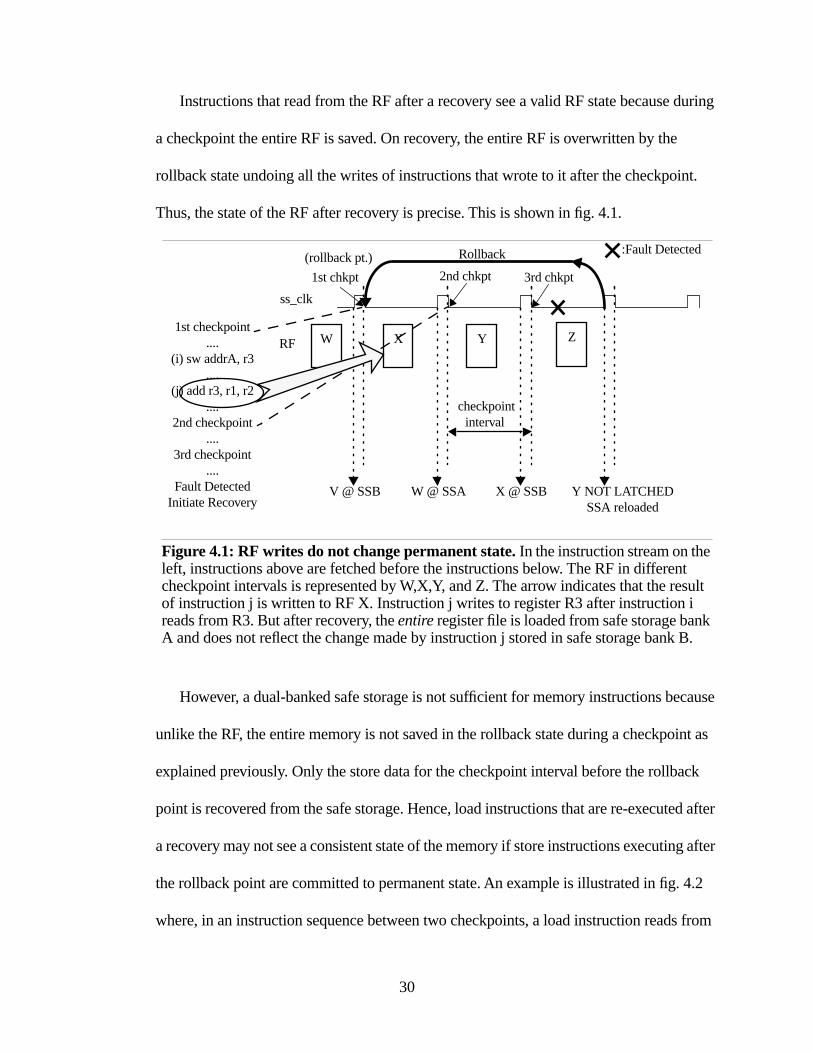
Instructions that read from the RF after a recovery see a valid RF state because during
a checkpoint the entire RF is saved. On recovery, the entire RF is overwritten by the
rollback state undoing all the writes of instructions that wrote to it after the checkpoint.
Thus, the state of the RF after recovery is precise. This is shown in fig. 4.1.
However, a dual-banked safe storage is not sufficient for memory instructions because
unlike the RF, the entire memory is not saved in the rollback state during a checkpoint as
explained previously. Only the store data for the checkpoint interval before the rollback
point is recovered from the safe storage. Hence, load instructions that are re-executed after
a recovery may not see a consistent state of the memory if store instructions executing after
the rollback point are committed to permanent state. An example is illustrated in fig. 4.2
where, in an instruction sequence between two checkpoints, a load instruction reads from
Figure 4.1: RF writes do not change permanent state. In the instruction stream on the left, instructions above are fetched before the instructions below. The RF in different checkpoint intervals is represented by W,X,Y, and Z. The arrow indicates that the result of instruction j is written to RF X. Instruction j writes to register R3 after instruction i reads from R3. But after recovery, the entire register file is loaded from safe storage bank A and does not reflect the change made by instruction j stored in safe storage bank B.
1st checkpoint....
(i) sw addrA, r3....
(j) add r3, r1, r2....
2nd checkpoint....
3rd checkpoint....
Fault DetectedInitiate Recovery
1st chkpt 2nd chkpt 3rd chkpt
Rollback :Fault Detected
W @ SSA X @ SSB Y NOT LATCHEDSSA reloaded
V @ SSB
ss_clk
YXW ZRF
checkpoint interval
(rollback pt.)
30

an address location that a store instruction succeeding it writes to. If the stores are
committed to permanent state too early, the load instruction may read the wrong data.
Architectural support to delay such stores from writing to permanent unrecoverable state
before it is safe to do so is called for.
In response to these requirements, TERPS employs a multi-phase commit protocol,
supported by three write buffers and the dual-bank safe storage, to ensure that no
instruction is permitted to commit to permanent unrecoverable state (i.e. the DRAM
system) until it is safe to do so. From fig. 4.2, it is clear that store data must be delayed to
memory so that on recovery, the state will be precise. To delay stores from writing their
data to permanent state, some temporary write buffers should be inserted between the CPU
and the memory system. Following the same example given in fig. 4.2, fig. 4.3 (a)
describes the TERPS mechanism equipped with two write buffers instead of one. For the
Figure 4.2: Store instructions that commit early may change permanent state. The figure illustrates a scenario with one write buffer where writes are committed to the memory system just after they are checkpointed. The load instructions i and j will incorrectly read the store data from instructions k and l after recovery as they were written to memory.
....1st checkpoint
....(i) lw r3, addrA(j) lw r5, addrB
....(k) sw addrA, r6(l) sw addrB, r3
(m) add r3, r1, r2....
2nd checkpoint....
3rd checkpoint....
Fault DetectedInitiate Recovery
P Q R SWB0
1st chkpt 2nd chkpt 3rd chkpt
Rollback :Fault Detected
P @ SSAP@ DRAM
Q @ SSBQ @ DRAM
R NOT LATCHEDR @ DRAMSSA reloaded
O @ SSBO@ DRAM
ss_clk
31

interval highlighted, the stores k and l write to addresses A and B after the loads i and j
have read from the same addresses. These stores write to WB0, named Q. After the third
checkpoint, a fault is detected and recovery is initiated. But at this point the instructions k
and l in Q have already been committed to the DRAM system. Hence when the loads i and
j are re-executed after recovery, they will incorrectly read the store data of the instructions
k and l. Thus, two write buffers do not delay the commitment of the store data adequately.
Figure 4.3: Multi-phase commit. This figure demonstrates how multi-phase commit is implemented to ensure all instructions following the checkpoint have not modified the process state before the commit point of their current checkpoint interval. In the instruction stream on the left, instructions above are fetched before the instructions below. (a) shows that two write buffers are insufficient whereas three write buffers, as shown in (b), are adequate.
....1st checkpoint
....(i) lw r3, addrA(j) lw r5, addrB
....(k) sw addrA, r6(l) sw addrB, r3
(m) add r3, r1, r2....
2nd checkpoint....
3rd checkpoint....
Fault DetectedInitiate Recovery
P
O P
Q
Q
R
O
R
P
SWB0
WB1
WB0
WB1
WB2
Q
P
P
Q
R
Q
R
N
S
O
1st chkpt 2nd chkpt 3rd chkpt
Rollback :Fault Detected
P @ SSAO @ DRAM
Q @ SSBP @ DRAM
R NOT LATCHEDQ @ DRAM SSA reloaded
O @ SSBN @ DRAM
O @ SSBM @ DRAM
P @ SSAN @ DRAM
Q @ SSBO @ DRAM
R NOT LATCHEDP @ DRAM
SSA reloaded
(a)
(b)
ss_clk
ss_clk
32

In fig. 4.3(b), three write buffers have been implemented. The additional third write buffer
postpones the commitment of Q to the DRAM by one checkpoint interval, preventing
instructions k and l from overwriting the values that i and j should read in case of a
recovery. Thus, three write buffers are adequate to accomplish correct multi-phase commit.
Consider a situation where the write buffer WB0, which contains the store data for a
particular checkpoint interval, is not saved into the rollback state. This case is shown in fig.
4.4. The stores in P have already been written to the DRAM by the time recovery is
initiated. After recovery, a load, shown to read data written by a store in P, may receive its
Figure 4.4: Importance of saving store data in the safe storage. Multi-phase commit implemented without saving the store data in the safe storage is shown. Loads k and l read data written by stores i and j. By the time the fault is detected, this store data (P) is written to the DRAM. But EMI might have corrupted it. After recovery, the loads k and l will again execute. They will correctly not read the store data due to stores m and n, but will read the corrupted data from the DRAM. Hence, on recovery it is necessary that a backup of the store data be brought back in to the system.
....(i) sw addrA, r6(j) sw addrB, r3
.....1st checkpoint
....(k) lw r3, addrA(l) lw r5, addrB
....(m) sw addrA, r6(n) sw addrB, r3
....2nd checkpoint
....3rd checkpoint
....Fault Detected
Initiate Recovery
O
PWB0
WB1
WB2
Q
P
P
Q
R
Q
R
N
S
O
:Fault Detected
M @ DRAM N @ DRAM O @ DRAM P* @ DRAM
ss_clk
1st chkpt 2nd chkpt 3rd chkpt
Rollback
P @ MC MC => DRAM
33

data from the DRAM. It would seem these stores, which represent a significant overhead
during checkpointing, do not need to be saved as they are present in the DRAM after a
recovery. However, it is important to note that during the interval highlighted in the fig. 4.4,
store data is being sent from the memory controller to the DRAM. Concurrently, a fault is
also detected. EMI effects may corrupt the buffer in the memory controller or the data on
the bus in transit to the DRAM rendering this data in the DRAM to be polluted. Saving the
WB0 contents is necessary for backup reasons and eventually the multi-phase commit
protocol will overwrite the DRAM with valid data using this backup after recovery.
If a fault is detected during recovery an invalid rollback state may be delivered to the
CPU and the system will recover to an invalid state. TERPS handles this issue by just
initiating recovery again using the same rollback state from the safe storage.
4.2Re-execution of instructions
Clearly, precise checkpointing and the multi-phase commit protocol work to resume
execution to a consistent and valid state. But, when instructions are re-executed, they write
their results to the system registers and memory again. This may trigger an event to reoccur
and this may change the correctness of computation.
One principle that the memory portion relies on is the fact that the memory system can
be read from or written to multiple times without side effects; reading from a given
memory location multiple times is the same as reading from that location once; writing to
a given memory location multiple times with the same value is the same as writing to that
location once. The RF also follows the same behavior. Hence, re-executing ALU and
memory instructions, provided we maintain in-order semantics for writes as discussed
above, does not affect the correctness of computation.
34

However, the I/O system does not behave like the memory system in this regard: I/O
reads and writes have side effects, and the last value written to an I/O location is not
necessarily the value read back from that location. For instance, a processor may be
outputting information to a increase an external counter which displays the number votes
for an electoral candidate. On re-execution of an I/O instruction after a recovery, if an
increment signal is re-sent, the counter would increment twice and show the incorrect
number of votes!
We are currently developing support for I/O semantics in TERPS. One crude yet
effective method is to checkpoint after every I/O request is executed. The CARER
mechanism [33] implements a similar protocol. But in TERPS the frequency of
checkpointing is dependant on the safe storage. The safe storage is slower because it is
made from an older process technology for better fault tolerance. The checkpoint interval
has to be long enough to meet the setup and hold times of the safe storage. Hence the
system may have to stall after every I/O request until a checkpoint can be established. This
would prove to be highly inefficient and its impact on performance would be significant if
I/O requests occurred frequently. For a more efficient implementation we are developing a
mechanism to support I/O semantics that incorporates the following characteristics:
1. Read and write buffers that are maintained by the I/O controller on a per-device basis
and that are enabled or disabled by the operating system.
2. Read and write transactions that are identified by a monotonically increasing unique
identifier.
3. A sliding window protocol between the CPU and the I/O controller to manage the
buffer contents so that any transaction is in one or more of the following states: (i)
35

buffered on the CPU, (ii) stored on the safe storage chip, (iii) buffered in the I/O
controller, or (iv) committed to the I/O system and out of the window of vulnerability.
We are currently modeling this mechanism in Verilog Hardware Description Language
and expect to integrate it into our TERPS system in the future.
36

Chapter 5
Implementation
5.1Basic Processor Architecture
The TERPS mechanism is general in nature and can be tied with any instruction-set
architecture. A microarchitecture’s existing logic for exception handling can be used to
generate a precise checkpoint and by augmenting it with the write buffers and checkpoint
rollback control logic, support for checkpoint and rollback recovery can be provided.
For implementation purposes, we chose the RiSC-16, 5-stage pipelined architecture as
the basic processor architecture. This architecture was selected because,
1. The author was familiar with the processor from the onset of development and the
architecture is well documented.
2. The design is not dependent on any particular instruction set; hence it was preferable to
use an existing instruction set.
3. A convincing “proof of concept” could be provided by this architecture, which, though
simple in design, is general enough to solve complex problems.
4. In order to have a successful physical prototype in an academic environment, the basic
processor architecture had to be simple.
37
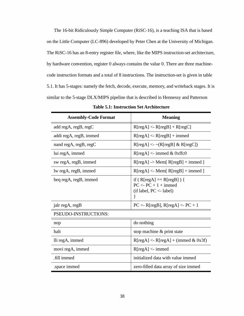
The 16-bit Ridiculously Simple Computer (RiSC-16), is a teaching ISA that is based
on the Little Computer (LC-896) developed by Peter Chen at the University of Michigan.
The RiSC-16 has an 8-entry register file, where, like the MIPS instruction-set architecture,
by hardware convention, register 0 always contains the value 0. There are three machine-
code instruction formats and a total of 8 instructions. The instruction-set is given in table
5.1. It has 5-stages: namely the fetch, decode, execute, memory, and writeback stages. It is
similar to the 5-stage DLX/MIPS pipeline that is described in Hennessy and Patterson
Table 5.1: Instruction Set Architecture
Assembly-Code Format Meaning
add regA, regB, regC R[regA] <- R[regB] + R[regC]
addi regA, regB, immed R[regA] <- R[regB] + immed
nand regA, regB, regC R[regA] <- ~(R[regB] & R[regC])
lui regA, immed R[regA] <- immed & 0xffc0
sw regA, regB, immed R[regA] -> Mem[ R[regB] + immed ]
lw regA, regB, immed R[regA] <- Mem[ R[regB] + immed ]
beq regA, regB, immed if ( R[regA] == R[regB] ) {PC <- PC + 1 + immed(if label, PC <- label)}
jalr regA, regB PC <- R[regB], R[regA] <- PC + 1
PSEUDO-INSTRUCTIONS:
nop do nothing
halt stop machine & print state
lli regA, immed R[regA] <- R[regA] + (immed & 0x3f)
movi regA, immed R[regA] <- immed
.fill immed initialized data with value immed
.space immed zero-filled data array of size immed
38

[40], and it fixes a few minor oversights, such as lack of forwarding to store data, lack of
forwarding to comparison logic in decode, implementing the 1-instruction delay slot, etc.
This pipeline adds in forwarding for store data and eliminates branch delay slots. As in the
DLX/MIPS, branches are predicted not taken, though implementations of more
sophisticated branch prediction are certainly possible.
5.2Implementation
The TERPS architecture is modeled in Verilog Hardware Description Language
(HDL), in which the modules are described by their logical behavior suitable for synthesis.
To guarantee the correctness of our mechanism at the behavioral level, a test bench is
written as a stimulus to simulate the behavior of the entire system. All simulations were
run in NC-Verilog which is a Logic Verification tool from the Cadence suite.
To support checkpoint and rollback recovery, three write buffers and a checkpoint latch
are added to the pipeline and a separate safe storage module was also developed to
interface with the processor core module. A detailed block diagram of the TERPS
architecture is given in fig.5.1. The fault detection signal is generated by a comparator
circuit on the CPU chip for the ease of development and testing.
Some of the important control mechanisms added to the existing control logic and
structure of the original pipeline for checkpointing and rollback were:
• checkpoint counter: This counter is responsible for the synchronization of the
checkpoint rollback mechanism. It is important for controlling many other signals and
their timing.
39

• chkpt: This signal indicates that a checkpoint is underway. The processor is stalled
during this time. It takes 7 CPU cycles to do a checkpoint in our implementation: 6-
cycles for transferring the WB2 to the memory controller over a 64-bit front-side bus
and 1-cycle for shifting the write buffer contents.
Figure 5.1: Detailed block diagram of the TERPS Processor Architecture. The RiSC-16, 5-stage pipeline modified to support checkpoint and rollback. The shaded boxes represent clocked registers; solid lines represent data paths and buses; and dotted lines represent control paths. A pipeline register is labelled with the two stages that it divides; for example, the pipeline register that divides the instruction fetch (IF) and instruction decode (ID) stages is called the IF/ID register. The prominent features added are the 3 write buffers (WB 0-2), the 512-bit checkpoint latch, the memory controller, checkpoint counter, detector latch, and checkpoint rollback control logic.
REGISTER FILE
SRC1SRC2
TGT
Program Counter
INSTRUCTIONMEMORY
OP rA rCrB PC
Sign-Ext-7
SRC1
TGT
SRC2
PCOP rT OPERAND2 OPERAND1
CTL6
EQ!CTL3
s2s1
CTL5
rT STORE DATAOP
+1
ADDRDATA IN
RF WRITE DATArT
DATA OUTCTL2 WEdmem
CTL1
WErf
FETCHSTAGE
DECODESTAGE
EXECUTESTAGE
MEMORYSTAGE
WRITEBACKSTAGE
RF WRITE DATArT
Left-Shift-6
MUXpc
MUXs2
MUXalu2
MUXalu1
MUXout
FUNCaluPstompSRC2 SRC1
ALU OUTPUT
OPERAND0
CTL4 MUXimm
MUXop0
CTL7
IF
ID
EX
MEM
ID
EX
MEM
WB
WB
END
PC
+1
ADD
Pstall
MCWB
0-2
DRAMC
HE
CK
PO
INT
LA
TC
H
CHECKPOINTROLLBACK BUS
ChkptRollback
Chkpt Counter
Chkpt SS_CLK, SS_SEL
FRONT SIDE BUS
R_m
ode,
R_s
tom
p
Detector Latch
M_stall
64
512
Chkpt_PC
RF
WB0
detector_RCtrl
SS_out_en
40

• detector_R: This signal goes high when a fault was registered. It is held high until
recovery is finished. It is used for timing and control purposes.
• RMODE: This signal, which makes the system go into recovery mode of operation,
goes high just before the safe storage is supposed to latch the data from the CPU. The
processor is stalled during RMODE.
• RMODE_stomp: When, the system goes into recovery mode, RMODE_stomp will
flush the pipeline, removing all “faulty” state.
• M_stall: This stalls the pipeline until the next checkpoint when there is a write request
but the write buffer,WB0, is full. The write buffers have 12-entries each.
• ss_sel: Used for selecting which bank of the safe storage the checkpointed rollback
state will be written to or read from.
• ss_out_en: This enables the output buffers of the safe storage so that it can output
rollback state information onto the checkpoint rollback bus.
The checkpoint latch contains the entire rollback state: 7 registers from the RF (RF0 is
always 0), the precise checkpoint PC, and the write buffer WB0. This 512-bit latch is
connected to a bi-directional checkpoint rollback bus which communicates with the safe
storage. To prevent the array of output buffers from pulling a large amount of current at the
same time, the bus is logically divided into 16, 32-bit sections to enable the bus in a
staggered manner.
The precise checkpoint PC is the PC of the next-to-commit instruction. In the 5-stage
RiSC-16 processor, the next-to-commit instruction is in the memory stage. If that
instruction is a nop, then the next valid instruction in the pipe is selected.
41

During a recovery, the checkpoint rollback bus has to be allowed a turn around time
before the safe storage sends data on it. This turn around time has been safely set to 20
CPU cycles.
To execute the multi-phase commit protocol correctly, the memory hierarchy has been
modified. Instead of directly accessing the main memory, a load instruction concurrently
checks in the write buffers WB0, WB1, WB2, the memory controller buffer, and the main
memory for data. If there are multiple matches for the same address, it gives priority in the
following order: WB0, WB1, WB2, memory controller buffer, and lastly main memory.
For simplicity, a 1-cycle memory access latency was assumed.
The safe storage module contains 2 banks A and B to store the newer and older
rollback states. Its slower clock (ss_clk) is generated by the CPU using the chkpt_counter.
The ss_sel signal from the CPU selects which bank the incoming rollback state should be
gated to during a checkpoint or from which bank should the CPU read data from during a
recovery.
Two working versions have been developed. One, which is fully synthesizable, yielded
a physical prototype which was fabricated through MOSIS in 0.25µm technology. It is a
functionally limited version (the write buffer is not saved in the safe storage during a
checkpoint) because it had to meet the constraints imposed on pin count by MOSIS. It
checkpoints every 128 cycles and can operate at 100MHz. It will be integrated with 2 safe
storage chips using 3D-IC technology at the Laboratory of Physical Sciences (LPS). This
prototype was developed for “proof of concept” and to test our capabilities in actually
fabricating a chip which we have done in a successful manner. The other version is a fully
functional one and its checkpoint frequency can be varied from 64 to 512 cycles per
42

checkpoint. We plan on fabricating it in the future utilizing the full capabilities of 3D-IC
technology. The performance analysis is based on this fully functional version.
5.2.1Logical Verification
This section is dedicated to enumerating the steps taken in verifying the logic
embedded in the design developed. NC Verilog is used to compile and run the verilog
code. A screen shot of the of the NC Verilog tool is shown in fig. 5.2.
Figure 5.2: Cadence NC Verilog. In this screen shot, you can observe the interface of the NC Verilog tool. The RF, PC, pipeline registers, and certain control signals are displayed by the simulation that is running.
43

After running the simulation, signals of particular interest can be selected using the
Design Browser and viewed in a timing diagram using the SimVision tool, which is
bundled with NC Verilog. A screen shot of the Design Browser is shown in fig. 5.3. Various
signals throughout the hierarchical modular structure of the Verilog code can be selected.
After selecting the various registers and wires in the Design Browser, the timing
diagram can be viewed in the SimVision waveform view. This is shown in fig. 5.4.
Figure 5.3: The Design Browser. This screen shot shows the interface of the Design Browser. On the left the various modules can be viewed in their hierarchical tree structure. On the right the various registers and wires are available for selection to be viewed in the timing diagram.
44

The checkpoint interval has been illustrated in the timing diagram. The RMODE signal
is high when the system is in recovery mode. It can be observed from the timing diagram
that a checkpoint is taken at the beginning of every checkpoint interval except for when the
system is in recovery mode. This is indicated by the ‘chkpt’ control signal. The recovery
penalty is shown to be 4 checkpoint intervals as explained previously. When a fault is
detected, the system goes into recovery mode and the pipeline is flushed using the
Figure 5.4: The Waveform view. This screen shot, shows the timing diagram of the simulation being run for selected signals. The signal names are displayed on the left hand side of the screen and from top to bottom are clk, ss_clk, chkpt, detector_out (the fault detection signal), detector_R, RMODE, RMODE_stomp, ss_out_en, ss_sel, data_bus_en, and the Checkpoint Rollback bus. The waveforms are displayed on the right side. The tool allows the user to zoom in and out, view the waveforms in motion, and place markers for debugging among many other features.
checkpoint interval rollback penalty
CPU to SS SS to CPUTAT
B A B A
not latched
45

‘RMODE_stomp’ control signal. The ‘ss_sel’ line indicates which bank of the safe storage
will be written to or read from. The bank, A or B, that is selected by the ‘ss_sel’ line is
marked in the diagram. When in recovery mode, the safe storage does not latch the
checkpointed state from the CPU into the safe storage (bank B in this case) as it may be
corrupted. The safe storage, after a bus turn around time (TAT), outputs the old rollback
state in bank B to the CPU. This is also marked in the figure. The system resumes normal
execution after recovery.
This timing diagram verifies that the logic design implemented in Verilog conforms to
the TERPS specifications.
5.3Safe Storage Implementation
This section discusses how the safe storage should be implemented to achieve low
susceptibility to fault tolerance. For our prototype, we fabricated the safe storage with a
0.5µm feature size, which is an older technology. It operates at a much lower frequency
(781.25 KHz) as compared to the CPU chip (100MHz). This frequency is set by the
checkpoint interval which is fixed to 128 CPU cycles for the prototype.
The safe storage is a memory that is specially designed to have significantly more EMI
tolerance than the processor. Most of the design techniques that can be used trade off speed
and/or die area to achieve better EMI tolerance. As high performance CPUs require both
speed and die area, the tradeoffs make it difficult for these techniques to be applied to a
processor and maintain its high performance.
Better EMI tolerance can be achieved using a variety of circuit, device, and process-
level techniques. Most of these are orthogonal to each other and may be used or left out
46

depending on the level of tolerance required by the system and the willingness of the
designer to accept the necessary tradeoffs.
The safe storage is implemented as a static RAM that uses cross-coupled inverters as
memory cells as opposed to a DRAM using a capacitor as the storage element. The
presence of the regenerative feedback on the inverter circuit makes it perform better as a
bistable circuit as compared to capacitor-based DRAMs.
The SRAM topologies shown in Fig. 5.5 can be compared based on their cell size,
static power consumption and (more importantly for this article) the static noise margin
(SNM). The SNM of a memory cell gives the required value of voltage change at the
inverter inputs to cause the cell to change state. Table 5.2 summarizes the features of each
configuration. It is a good measure of the amount of spurious signal needed at the memory
cell inputs to corrupt its state.
The SNM of different memory cell configurations has been extensively studied (a very
good example is Seevinck [42]). These studies show that the 6T configuration almost
always has higher SNM. The 4T configuration can approach or even equal the 6T SNM but
BLBL
WL WL
BLBL
WL WL
BLBL
WL WL
Figure 5.5: 3 possible SRAM memory cell implementations. Fig. (a) shows the conventional six-transistor (6T) cell, fig. (b) shows the four- transistor (4T) cell, and fig. (c) shows a four-transistor loadless (4TLL) memory cell configuration.
(a) (c)(b)
BLBLBLBLBLBL
WLWLWLWLWLWL
47

at the expense of both its size and DC power consumption. This makes the 6T memory cell
the best choice if higher EMI tolerance is needed.
The soft-error rate (SER) of SRAMs in the presence of alpha particles has also been
widely studied [43][44]. It has been shown that maximizing the stored charge in the
memory cell (output nodes of the inverters in Fig. 5.5) makes it harder for alpha-particles
to erroneously cause state changes in the memory cell, resulting in better SER. The most
common way to increase this stored charge is to increase the parasitic capacitance of the
cell output nodes so that more charge is stored for a given supply voltage. This capacitance
is increased using device-level techniques enlarging the cell area to increase the parasitic
diffusion capacitances. Hence, higher capacitance is achieved at the expense of a larger
cell area. Process-level techniques can also be used where grounded polysilicon layers are
added to increase overlap capacitance or to completely fabricate the PMOS loads in
polysilicon. In this case, higher capacitance is achieved in exchange for process
complexity.
Techniques to improve SER also improve EMI tolerance. Achieving better SER by
increasing the charge stored in the memory cell results in better EMI tolerance because
Table 5.2: Features of different SRAM topologies
Topology SizeDC Power
ConsumptionSNM
6T Big Very Minimal High
4T Medium Potentially Significant
Low-high
4TLL Small Very Minimal Low-medium
48
larger EMI signal powers are required to induce a voltage in the system that is large
enough to exceed the cell's SNM to corrupt the cell's state.
The same principle can be applied to the entire safe-storage system and not just the
storage cells. Using transistors with larger areas and powered by a higher supply voltage
will result in increased charge stored within the system. This increased charge require
larger amounts of EMI to push around. Since the safe-storage area needs larger transistors
and higher supply voltages to increase the stored charge, it is fabricated using a larger
feature size process that is about two or more process generations older than the one used
for the CPU. This exemplifies the tradeoffs between speed and EMI tolerance needed to
implement the system.
Using the previous techniques, the circuitry within the safe-storage can be made to
tolerate higher-levels of EMI. Care has to be taken to ensure that a specific subset of the
communication between the CPU and the safe-storage be reliable. One way this could be
done is to use differential signaling between the safe-storage and the CPU. Common node
noise caused by the EMI will be cancelled and with proper care, induced differential mode
noise will be minimal. EMI coupling must be minimized to accomplish this goal.
Interconnect lengths must be minimized, along with current loop areas (that function as
antennas) formed by the interconnect. This can be accomplished by using differential
signal interconnects placed very close to each other.
Achieving all of this is facilitated by the 3D integration technology used by the system.
This relaxes the pin limitations imposed by packaging constraints in conventional systems.
This makes additional input/output pads available to the designer, with the added benefit
that inter-die interconnects are going to be considerably shorter because of the chip-
49

stacking. This makes possible the use of short, very wide, differential buses needed for
EMI-tolerant communication. An additional benefit of 3D chip integration is the
possibility of using die-level shielding mechanisms to protect the safe-storage core from
EMI. Our group’s efforts in 3D integration are described in a recent article [45].
As a summary of this section, the safe-storage will use six-transistor memory cells to
maximize storage stability. A better EMI tolerance can be achieved by increasing the
amount of stored charge within the system. This can be done by using additional grounded
polysilicon layers to increase signal overlap capacitances, by increasing transistor sizes to
increase diffusion capacitances, and increasing the supply voltage. The safe storage can be
fabricated using a process technology that is approximately two generations older than the
CPU. Lastly, 3D chip integration is used to interconnect the safe-storage and the CPU
together. This technology removes pin limitations imposed by package constraints and
makes possible the use of a short, very-wide differential bus. 3D integration also makes
possible the use of various chip-level shielding schemes to further protect the safe-storage
from EMI.
50
Chapter 6
Results
6.1Performance Analysis
This section presents the checkpoint rollback recovery mechanism and the multi-phase
commit protocol’s effect on the overall performance of a processor. During the normal
execution of instructions, the interaction with the checkpointing mechanism is limited to
the write buffers and hence its impact on performance is low. The overhead is primarily
due to the time taken to establish a checkpoint and how frequently a checkpoint is taken.
As checkpointing is done in a periodic fashion, performance is similar for different
benchmarks when TERPS is operating at a particular checkpointing time interval.
However, memory intensive benchmarks may slow down forward progress significantly if
they regularly fill up the write buffer quickly and therefore stall the machine. Hence it is
important to select the proper write buffer size. In general, 30% of instructions are memory
instructions and 10% of these are stores [40]. We have chosen 4 different checkpointing
time intervals (64, 128, 256, 512) to show the impact of checkpointing on performance and
the corresponding write buffer size is shown in table 6.1.
51

The benchmarks used were:
1. Laplace: Uses numerical methods to approximate Laplace's equation by averaging.
2. Vector Addition: Adds 2 vectors of size 10,000. Memory intensive.
3. Sample: Implements various basic functions which are seen in many programs like
summation, factorial, etc.
4. Horner: Implements Horner's method for evaluating a polynomial and compares it
with another less efficient method.
The C compiler for RiSC-16 microprocessor (ver. 1.50) developed by Afshin Sepehri
and Bruce Jacob [46] was used to compile Sample and Horner.
The performance impact due to these benchmarks is shown in fig.6.1. All results are
with a 64-bit frontside bus. The performance impact of various benchmarks for a particular
checkpointing time interval is relatively the same. This is seen because the write buffers
did not fill up often even in the case of the memory intensive Vector Addition benchmark
and hence checkpointing, in this scenario, does nothing to worsen the computational speed
of the pipeline. These results support the criteria for selecting the size of the write buffers.
The checkpointing mechanism stalls the pipeline during a checkpoint and takes a
checkpoint independent of the state of the system. So the performance overhead is mainly
Table 6.1: Write buffer size
CPU cycles per checkpoint
Write buffer size
64 8
128 12
256 24
512 48
52

due to the stalling of the pipeline during a checkpoint and how frequent a checkpoint is
made.
During a checkpoint, the rollback state is saved into the checkpoint latch, the store data
in the last write buffer WB2 is transferred over the 64-bit frontside bus to the memory
controller, and then the write buffer WB2 will be overwritten by WB1 and WB1 by WB0.
The overhead of stalling the pipeline and performing a checkpoint is prominent when
checkpointing is done more frequently as can be observed from the chart. It would seem
that as the checkpointing interval is increased the performance would improve drastically.
However, when checkpointing is done less frequently the size of the write buffers has to
increase to accommodate more store data. Correspondingly, the time required to establish
a checkpoint will increase as it takes more cycles to write the store data in the write buffer
Figure 6.1: Performance Overhead due to checkpointing. Four benchmarks were run on the TERPS system at four different checkpointing time intervals.
Performance Overhead (64-bit frontside bus)
0123456789
10
64 128 256 512Checkpointing Time Interval
(CPU cycles/checkpoint)
Ove
rhea
d (%
)
LaplaceVectorAddSampleHorner
53
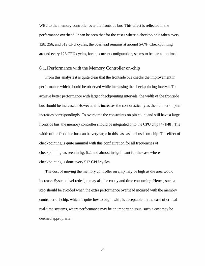
WB2 to the memory controller over the frontside bus. This effect is reflected in the
performance overhead. It can be seen that for the cases where a checkpoint is taken every
128, 256, and 512 CPU cycles, the overhead remains at around 5-6%. Checkpointing
around every 128 CPU cycles, for the current configuration, seems to be pareto-optimal.
6.1.1Performance with the Memory Controller on-chip
From this analysis it is quite clear that the frontside bus checks the improvement in
performance which should be observed while increasing the checkpointing interval. To
achieve better performance with larger checkpointing intervals, the width of the frontside
bus should be increased. However, this increases the cost drastically as the number of pins
increases correspondingly. To overcome the constraints on pin count and still have a large
frontside bus, the memory controller should be integrated onto the CPU chip [47][48]. The
width of the frontside bus can be very large in this case as the bus is on-chip. The effect of
checkpointing is quite minimal with this configuration for all frequencies of
checkpointing, as seen in fig. 6.2, and almost insignificant for the case where
checkpointing is done every 512 CPU cycles.
The cost of moving the memory controller on chip may be high as die area would
increase. System level redesign may also be costly and time consuming. Hence, such a
step should be avoided when the extra performance overhead incurred with the memory
controller off-chip, which is quite low to begin with, is acceptable. In the case of critical
real-time systems, where performance may be an important issue, such a cost may be
deemed appropriate.
54
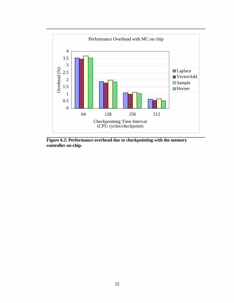
Figure 6.2: Performance overhead due to checkpointing with the memory controller on-chip.
Performance Overhead with MC on chip
0
0.5
1
1.5
2
2.5
3
3.5
4
64 128 256 512
Checkpointing Time Interval (CPU cycles/checkpoint)
Ove
rhea
d (%
)
LaplaceVectorAddSampleHorner
55

Chapter 7
Conclusions and Future Work
In this thesis, the threat of intentional EMI to electronic systems was addressed by
introducing a fault tolerant architecture, TERPS (The Embedded Reliable Processing
System). It can significantly lower the susceptibility of a processing system against EMI-
induced transient faults by restricting the area of vulnerability to a small section of a CPU
and a safe storage device that uses technology which is relatively much more EMI-
tolerant. The system provides this increased resistance to EMI by transparently performing
checkpoint rollback recovery operations between the CPU and safe storage, and by
instituting a multi-phase commit protocol between the CPU and memory controller.
TERPS can recover from a system wide failure scenario (i.e.one in which nearly every
transistor on a CPU is affected), while most checkpoint rollback recovery techniques
recover from single error event faults.
The TERPS mechanism occupies a region of the design space between schemes that
rely primarily on redundant hardware (e.g. n-modular redundancy) and schemes that rely
primarily on redundant computation (e.g. redundant execution-in-place). TERPS
represents a trade-off of a moderate hardware overhead (the extra safe storage chip and
write buffers) and a minimal performance overhead.
56

The TERPS mechanism has reduced the scope of vulnerability to only the safe storage
and the control logic to execute the checkpoint mechanism itself from a situation where
everything could go wrong. A comprehensive discussion on safe storage fault tolerance
was provided. The control logic used to control the checkpoint mechanism can be made
more fault tolerant by employing differential signaling based techniques.
A correctness of design was provided by stating the necessary and sufficient conditions
for the checkpoint rollback recovery mechanism to work and then showing how TERPS
supported them. Furthermore, our implementation, developed in Verilog, was functionally
verified by industry standard logic verification tools. We have also built a physical
prototype system on 0.5 µm and 0.25 µm processes through MOSIS. The
photomicrographs of the chips we fabricated are shown in fig. 7.1.
The performance impact of checkpointing (i.e. the cost of stalling during checkpoints
and buffer overflows) has been kept minimal (~6% for checkpointing every 128 CPU
Figure 7.1: Photomicrographs of chips fabricated via MOSIS. (a) Processor core fabricated via MOSIS at TSMC in a 0.25 µm feature size with a die area of 10.89 mm2, a pad count of 100, and in a MQFP package. (b) Safe Storage chip fabricated via MOSIS at AMI in a 0.5 µm feature size with a die area of 5.29 mm2, a pad count of 84, and in a PLCC package.
(a) Processor Core (b) Safe Storage
57

cycles) with the aid of high-bandwidth, low latency enabling technologies like 3D
integration. Two memory controller configurations were described; one with the memory
controller off-chip and another with the memory controller on-chip. The latter shows better
performance (~2% for checkpointing every 128 CPU cycles) as compared to the former
but with added cost.
The fabrication of a 3-D integrated chip is important in proving the feasibility of the
system and this will be completed soon. In the near future, we plan to expand the sphere of
protection offered by TERPS by encompassing more system elements (e.g. I/O) into the
TERPS mechanism.
If the RF detection latency can be accurately determined, the rollback penalty can be
reduced in certain instances by recovering to the newer rollback state in the safe storage.
Methods of enabling a checkpointing mechanism in which the checkpointing interval can
be varied dynamically to improve performance should be explored. This may be useful
when moving from one place to another where the EMI levels may change. In an
environment with low EMI levels, the checkpoint interval can be large to improve
performance while in a harsh EMI environment, the rate of checkpointing can be increased
to reduce the rollback penalty. Another dynamic checkpointing mechanism may initiate a
checkpoint every time the write buffer is full hence removing performance penalties due to
write buffer related stalls.
58
REFERENCES
[1] J. Bethune, S.S. Conroy, “Newsline: The New Cold War: Defending Against
Criminal EMI”, Compliance Engineering, May-June 2001. Available:
http://www.ce-mag.com/archive/01/05/news.html
[2] E. Sicard, C.Marot, J. Y. Fourniols, M. Ramdani, “Electromagnetic Compatibility
for Integrated Circuits”, Techniques l'ingénieur/Techniques for Engineers, 2003, to
be published.
[3] F. Fiori, S. Benelli, G. Gaidano, V. Pozzolo, “Investigation on VLSI’s Input Ports
Susceptibility to Conducted RF Interference”, IEEE International Symposium on
Electromagnetic Compatibility, 18-22 Aug. 1997, pp. 326 -329.
[4] D. J. Kenneally, D.S. Koellen, S. Epshtein, “RF Upset Susceptibility of CMOS and
Low Power Schottky D-Type, Flip-Flops”, IEEE National Symposium on
Electromagnetic Compatibility, 23-25 May 1989, pp. 190 -195.
[5] F. Fiori, “Integrated Circuit Susceptibility to Conducted RF Interference”,
Compliance Engineering 17, no. 8 (2000), pp. 40-49.
[6] S. Baffreau, S. Bendhia, M. Ramdani, E.Sicard, “Characterisation of
Microcontroller Susceptibility to Radio Frequency Interference”, Proc. of the
Fourth IEEE International Caracas Conference on Devices, Circuits and Systems,
17-19 April 2002, pp. I031-1 -I031-5.
[7] K. M. Strohm, J. Büchler, E. Kasper, J. F. Luy, P. Russer, ``Millimeter Wave
Transmitter and Receiver Circuits on High Resistivity Silcon'', IEE Colloquium on
59

Microwave and Millimeter Wave Monolithic Integrated Circuits ,
(London,England), 11 Nov. 1988, Digest No: 1988/117, pp. 11/1-11/4
[8] V. Milanovic, M. Gaitan, J.C. Marshall, M.E. Zaghloul, “CMOS foundry
implementation of Schottky diodes for RF detection”, Electron Devices, IEEE
Transactions on, Volume 43, Issue 12 ,Dec. 1996, pp. 2210 -2214.
[9] K. Banerjee, S. J. Souri, P. Kapur, and K. C. Saraswat, “3-D ICs: A Novel Chip
Design for Improving Deep Submicrometer Interconnect Performance and
Systems-on-Chip Integration ”, Proceedings of the IEEE, Special Issue,
Interconnections- Addressing The Next Challenge of IC Technology, Vol. 89, No.
5, pp. 602-633, May 2001. (INVITED)
[10] N. Savage, “Linking with Light”, IEEE Spectrum, vol. 39, issue 8, Aug. 2002, pp.
32-36.
[11] P. N. Glaskowsky, “Rambus Rolls Out Yellowstone, FlexPhase Circuit Design to
Speed DRAMs and More”, Microprocessor Report, July 15, 2002
[12] B. Randell, P. Lee, P. C. Treleaven, “Reliability Issues in Computing System
Design”, ACM Computing Surveys, vol.10 , issue 2, June 1978, pp. 123 - 165.
[13] M. Peercy, P. Banerjee, “Fault Tolerant VLSI Systems”, Proceedings of the IEEE,
Vol. 81, No. 5, May 1993, pp. 745-758.
[14] M. Franklin, “Incorporating Fault Tolerance in Superscalar Processors”, Proc. 3rd
International Conference on High Performance Computing, 19-22 Dec. 1996, pp.
301 -306.
60
[15] J. B. Nickel, A.K. Somani, “REESE: A Method of Soft Error Detection in
Microprocessors”, Proc. The International Conference on Dependable Systems and
Networks, 1-4 July 2001, pp. 401 -410.
[16] C. Weaver, T.Austin, “A Fault Tolerant Approach to Microprocessor Design”, Proc.
The International Conference on Dependable Systems and Networks, 1-4 July
2001, pp. 411-420.
[17] T. M. Austin, “DIVA: A Reliable Substrate for Deep Submicron Microarchitecture
Design”, MICRO-32. Proc. 32nd Annual International Symposium on
Microarchitecture, 16-18, Nov. 1999, pp. 196 -207.
[18] A. Avizieniz et al., “The STAR (self testing and repairing) computer: an
investigation of the theory and practice of fault tolerant computer design”, IEEE
Trans. on Comp. C-20, 11, Nov. 1971, 1312-1321.
[19] R. Koo and S. Toueg, “Checkpointing and Rollback-Recovery for Distributed
Systems”, IEEE Trans. on Software Engin. SE-13,(1), Jan. 1987, pp. 23-31.
[20] K. M. Chandy and C. V. Ramamoorthy,“Rollback and Recovery Strategies for
Computer Programs”, IEEE Transactions on Computers, Vol. C-21, pp. 546-556,
June 1972.
[21] J. S. Upadhyaya and K. K. Saluja,“A Watchdog Processor Based General Rollback
Technique with Multiple Retries”, IEEE Transactions on Software Engineering,
Vol. SE-12, pp. 87-95, Jan 1986.
[22] K. G. Shin, T. H. Lin, and Y. H. Lee, “Optimal Checkpointing of Real-Time Tasks”,
61

IEEE Transactions on Computers, Vol. C-36, pp. 1328-1341, Nov 1987.
[23] M. L. Ciacelli, “Fault Handling on the IBM 4341 Processor”, 11th Fault-Tolerant
Computing Symposium, Portland, Maine, June 1981, pp. 9-12.
[24] M.M. Tsao et al. “The Design of C.fast: A Single Chip Fault Tolerant
Microprocessor”, Proc. 12th Int. FTCS, June 1982, pp. 63-69.
[25] L. Spainhower et al., “Design for fault-tolerance in system ES/9000 model 900,”
Proc. 22th Int.Symp. on Fault-Tolerant Computing, July 1992, pp. 38–47.
[26] Y. Tamir, M. Liang, T. Lai, and M. Tremblay, “The UCLA Mirror Processor: A
Building Block for Self-Checking Self-Repairing Computing Nodes”, Proc. 21st
Int'l Symp. Fault-Tolerant Computing, June 1991, pp. 178-185.
[27] N. J. Alewine, S.-K. Chen, W.K. Fuchs, W.-M. W. Hwu “Compiler-Assisted
Multiple Instruction Rollback Recovery Using A Read Buffer”, IEEE Transactions
on Computers, Volume: 44 Issue: 9 , Sept. 1995, pp. 1096 -1107.
[28] Yuval Tamir, Marc Tremblay, and David A. Rennels, “The Implementation and
Application of Micro Rollback in Fault-Tolerant VLSI Systems,” 18th Fault-
Tolerant Computing Symposium, Tokyo, Japan, June 1988, pp. 234-239.
[29] Y. Tamir, M. Tremblay, “High Performance Fault-Tolerant VLSI Systems using
Micro Rollback”, IEEE Transactions on Computers, Volume: 39 Issue: 4 , April
1990, pp. 548 -554.
[30] C.-C.J. Li, S.-K. Chen, W. K. Fuchs, W.-m.W. Hwu, “Compiler-based Multiple
Instruction Retry”, IEEE Transactions on Computers, Volume: 44 Issue: 1 , Jan.
62

1995, pp. 35 -46.
[31] Shyh-kwei Chen and W. Kent Fuchs, “Compiler-Assisted Multiple Instruction
Word Retry for VLIW Architectures”, IEEE Transactions on Parallel and
Distributed Systems, vol. 12(12), Dec. 2001, pp. 1293-1304.
[32] N. S. Bowen, D. J. Pradhan, “Virtual checkpoints: Architecture and performance,”
IEEE Trans. on Computers, vol. 41, no. 5, May 1992, pp 516–525.
[33] D. B. Hunt and P. N. Marinos, “A general purpose cache-aided error recovery
(CARER) technique”, Proc. 17th Int. Symp. on Fault-Tolerant Computing, 1987,
pp. 170–175.
[34] B. Janssens and W. Fuchs, “The performance of cache-based error recovery in
multiprocessors”, IEEE Transactions on Parallel and Distributed Systems, 5(10),
Oct.1994, pp.1033-1043,.
[35] K.-L. Wu, W. K. Fuchs, and J. H. Patel, “Error recovery in shared memory
multiprocessors using private caches,” IEEE Trans. on Parallel and Distributed
Systems, vol. 1, no. 2, Apr. 1990, pp. 231–240.
[36] M. Prvulovic , J. Torrellas, Z. Zhang. “ReVive: Cost-Effective Architectural
Support for Rollback Recovery in Shared-Memory Multiprocessors”, Proc. of the
29th Annual International Symposium on Computer Architecture, May 2002,
pp.111-122.
[37] D. J. Sorin , M. M. K. Martin, M. D. Hill, and D. A. Wood, “SafetyNet : Improving
the Availability of Shared Memory Multiprocessors with Global Checkpoint/
63
Recovery”, Proc. of the 29th Annual International Symposium on Computer
Architecture, May 2002, pp. 123-134.
[38] W.-M. W. Hwu, Y.N. Patt, “Checkpoint Repair for Out-of-order Execution
Machines”, Proc. of the 14th annual International Symposium on Computer
Architecture, June 1987, pp. 18-26.
[39] J. E. Smith and A. R. Pleszkun, “Implementing Precise Interrupts in Pipelined
Processors”, IEEE Trans. Computers, C-37(5), May 1988, pp.562--573.
[40] J. L. Hennessy and D. A. Patterson, “Computer Architecture A Quantitative
Approach”, Morgan Kaufmann Publishers Inc., 2 nd edition, 1996. ISBN 1-55860-
329-8.
[41] G. S. Sohi , S. Vajapeyam, “Instruction Issue Logic for High-performance,
Interruptable Pipelined Processors”, Proceedings of The 14th Annual International
Symposium on Computer Architecture, June 02-05, 1987, pp. 27-34.
[42] E.Seevinck, F.J.List and J.Lohstroh, "Static-noise margin analysis of MOS SRAM
cells," IEEE J.Solid-State Circuits, vol SC-22, no.5, Oct.1987, pp.748-754.
[43] K.Ishibashi et al, "An alpha-immune, 2-V supply voltage SRAM using a
polysilicon PMOS load cell," IEEE J.Solid-State Circuits, vol SC-25, no.1,
Feb.1990, pp. 55-60.
[44] H.Sato et al, "A 500-MHz pipeline burst SRAM with improved SER immunity,"
IEEE J.Solid-State Circuits, vol. SC-34, no.11, Nov.1999, pp. 1571-1579.
[45] G. Metze, M. Khbeis, N. Goldsman, B. Jacob. "Heterogeneous Integration: 3D
64
Integration of Components with Different Electrical Functionality or Material
Systems." NSA Tech Trend, to appear.
[46] A. Sepehri, B. Jacob, “C Compiler for RiSC-16 Microprocessor”, Available: http:/
/www.ece.umd.edu/~afshin/rcc-report.htm
[47] Chetana N. Keltcher, “The AMD Hammer Processor Core”.
[48] Douglas Sanders, “Designing a PC with DECchip 21066”, Proc. of IEEE
Compcon, 1994, pp.414-417.
65